July 1999 • NREL/SR-520-26648 S. Guha United Solar Systems Corp. Troy, Michigan High-Efficiency Triple-Junction Amorphous Silicon Alloy Photovoltaic Technology Annual Technical Progress Report 6 March 1998 — 5 March 1999 National Renewable Energy Laboratory 1617 Cole Boulevard Golden, Colorado 80401-3393 NREL is a U.S. Department of Energy Laboratory Operated by Midwest Research Institute • Battelle • Bechtel Contract No. DE-AC36-98-GO10337
Annual Technical Progress Report6 March 1998 — 5 March 1999
S. GuhaUnited Solar Systems Corp.Troy, Michigan
NREL Technical Monitor: K. Zweibel
Prepared under Subcontract No. ZAK-8-17619-09
National Renewable Energy Laboratory1617 Cole BoulevardGolden, Colorado 80401-3393
NREL is a U.S. Department of Energy LaboratoryOperated by Midwest Research Institute •••• Battelle •••• Bechtel
Contract No. DE-AC36-98-GO10337
NOTICE
This report was prepared as an account of work sponsored by an agency of the United Statesgovernment. Neither the United States government nor any agency thereof, nor any of their employees,makes any warranty, express or implied, or assumes any legal liability or responsibility for the accuracy,completeness, or usefulness of any information, apparatus, product, or process disclosed, or representsthat its use would not infringe privately owned rights. Reference herein to any specific commercialproduct, process, or service by trade name, trademark, manufacturer, or otherwise does not necessarilyconstitute or imply its endorsement, recommendation, or favoring by the United States government or anyagency thereof. The views and opinions of authors expressed herein do not necessarily state or reflectthose of the United States government or any agency thereof.
Available to DOE and DOE contractors from:Office of Scientific and Technical Information (OSTI)P.O. Box 62Oak Ridge, TN 37831
Prices available by calling 423-576-8401
Available to the public from:National Technical Information Service (NTIS)U.S. Department of Commerce5285 Port Royal RoadSpringfield, VA 22161703-605-6000 or 800-553-6847orDOE Information Bridgehttp://www.doe.gov/bridge/home.html
Printed on paper containing at least 50% wastepaper, including 20% postconsumer waste
i
Preface
This Annual Subcontract Report covers the work performed by United Solar Systems Corp. for theperiod March 6, 1998 to March 5, 1999 under DOE/NREL Subcontract No. ZAK-8-17619-09. Thefollowing personnel participated in the research program.
A. Banerjee, E. Chen, J. Edens, T . Glatfelter, S. Guha (Principal Investigator),G. Hammond, M. Hopson, N. Jackett , K. Lord, A. Mohsin, J. Noch, T . Palmer, D.Wolf, B. Yan, J. Yang, and K. Younan.
Collaboration with the Colorado School of Mines, University of Oregon, National Renewable EnergyLaboratory, and Energy Conversion Devices, Inc. is acknowledged. We would like to thank V. Trudeaufor preparation of this report.
ii
Table of Contents
Pag e
Preface i
Table of Contents ii
List of Figures iv
List of Tables vi
Executive Summary 1
Section 1 Introduction 4
Section 2 Amorphous Silicon Alloy Materials and Solar CellsNear The Threshold of Microcrystallinity 5
I nt ro duc ti on 5
Ex per i ment al Res ul t s an d Di sc uss io n 5
Su mmar y 19
Sec ti on 3 St at us of Smal l Ar ea Comp onen t and Mul ti j unct io n Cel ls Dep osi te d wi th RF and MVHF at 3- 5 Å/ s 22
I nt ro duc ti on 22
St at us of 3 Å/ s RF a- Si Al l oy So la r Cel l s 22
Mod if i ed Ve ry -Hi gh -Fr eq uen cy Pl as ma En han ced Che mi cal Va por Dep os it i on ( MVHF- PEC VD): Pl as ma Pr ope rt i es an dSo la r Cel l Dep os it i on 23
Com par is on of t he St ab il i ty of RF an d MVHF a- Si Al l oySo la r Cel l s 36
iii
Pag e
Sec ti on 4 St at us of Amor pho us Si li con Al lo y Comp onen t and Mul ti j unct io nCel ls and Modu le s Dep osi te d i n a Lar ge- Ar ea Rea cto r 38
I nt rod uct i on 38
Dev i ce Fa bri c at ion an d Mea sur eme nt 38
St ab il i ty St ud ie s 39
Res ul t s of Com pon ent Cel l s 39
Res ul t s of Tr ip le -j un ct io n Cel l s 42
Mod ul e Res ul t s 48
NRE L Mea sur eme nt of Mod ul es 54
New Wor ld Rec or d St ab le 10 .5 % Mod ul e Ef f ic ie ncy 55
Su mmar y of La rg e-a re a Res ul t s 60
La rg e-a re a Pr ot ot yp e Mod ul es 60
I EEE St d 12 62- 19 95 Qua li f ic at io n of Mod ul es 61
Sec ti on 5 Fut ur e Di rec ti ons 67
Ref er ence s 68
iv
List of Figures
Pa ge
1. Hy dro gen ev ol ut io n sp ect r a f or ( a) t he l ow di l ut io n an d( b) t he hi gh di l ut io n sa mpl es . 7
2. Deu te ri um ev ol ut io n sp ect r um f ro m t he de ut er at ed sa mpl e. 8
3. Ram an sp ect r a ve rs us hy dr oge n di l ut io n of f our sa mpl es: ( a) no di l ut io n, ( b) l ow di l ut io n, ( c) med iu m di l ut io n, an d ( d) hi gh di l ut io n. 9
4. Sc hema ti c di ag ra m of f our so la r ce ll st r uct ur es : ( a) si ng le ,( b) sa me ba ndg ap do ubl e, ( c) du al ba ndg ap do ubl e, an d( d) t ri pl e j unc ti on s. 11
5. I ni ti al J- V ch ar ac te ri st i c of an a- Si Ge al l oy p i n so la r ce ll . 13
6. I ni ti al J- V ch ar act er i st ic of t he 14 .6 % t ri pl e- ju nct i on ce ll . 15
7. Qua nt um ef f ic ie ncy of t he de vi ce sh own i n Fi g. 6. 16
8. I ni ti al J- V ch ar act er i st ic of t he 15 .2 % t ri pl e- ju nct i on ce ll . 17
9. Quan tu m ef f ic ie ncy of t he de vi ce sh own i n Fi g. 8. 18
10 . I ni ti al J- V ch ar act er i st ic of an a- Si al l oy t op ce ll de pos it ed at ~1 Å/ s. 20
11 . I ni ti al J- V ch ar act er i st ic of an a- Si al l oy t op ce ll de pos it ed at ~8 Å / sby MVHF . 21
12 . En erg y di st r ib ut io n of po si ti ve i ons r eac hed t he su bst r at e i na H2 pl as ma ex ci te d by 75 MHz VHF . 24
13 . Po si ti ve i on en er gy di st r ib ut io n of a H2 pl as ma ex ci te d by 13 .5 6 MHz RF. 25
14 . Com par is on of t he po si ti ve i on en er gy di st r ib ut io n of pu re H2 pl as ma an dpl as ma wi th H2 an d Si H4 mi xt ur e. 27
15 . I on en er gy di st r ib ut io n wi th t wo VHF po wer s f or a H2 pl as ma at 0. 1 t or r. 28
16 . I on en er gy di st r ib ut io n wi th t wo RF po wer s f or a H2 pl as ma at 0. 1 t or r. 29
17 . Cha ra ct er is ti c pa ra met er s f or a- Si al l oy so lar ce ll s mad e at di f fe re ntSi H4 f lo w r at es. 33
v
Pa ge
18 . Fi l l f act or s of a- Si Ge al l oy so la r ce ll s on SS as a f unc ti on of H2 f lo w r at e. 34
19 . Fi l l f act or s of a- Si Ge al l oy so la r ce ll s on BR as a f unc ti on of H2 f lo w r at e. 35
20 . I ni ti al J- V ch ar act er i st ic of a t ri pl e- ju nct i on de vi ce of ef f ic ie ncy 14 .5 %. 44
21 . I ni ti al Q ch ar act er i st ic of t he ce ll sh own i n Fi g. 20 . 45
22 . St ab le J- V ch ar act er i st ic of a t ri pl e- ju nct i on de vi ce of ef f ic ie ncy 12 .9 %. 46
23 . St ab le Q ch ar act er i st ic of t he cel l sh own i n Fi g. 22 . 47
24 . I ni ti al I -V ch ar act er i st ic of a ba re mi ni -mo dul e of ap er tu re ar ea 44 .3 9 cm2. 49
25 . St ab le I -V ch ar act er i st ic of an en cap sul at ed mi ni -mo dul e. 51
26 . St ab il i ty of en cap sul at ed mod ul es of ap er tu re ar ea ~4 50 cm2. 53
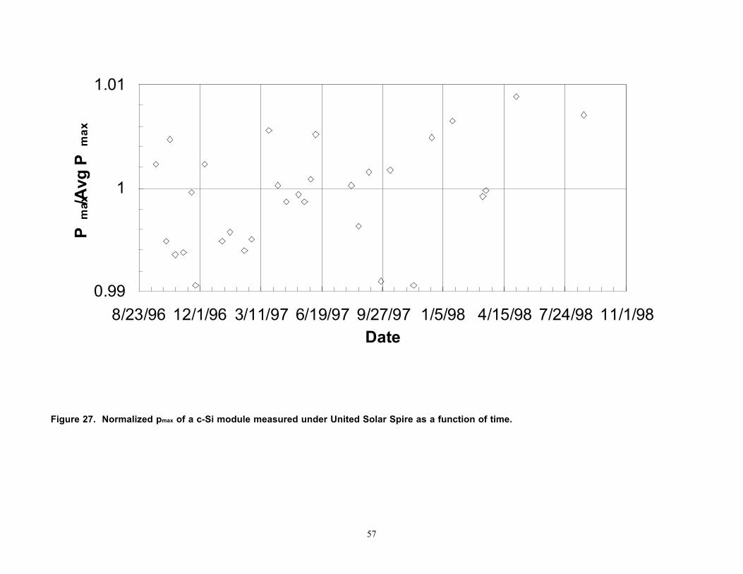
27 . Nor mal i zed Pmax of a c- Si mod ul e mea sur ed un der Uni t ed So la r Sp ir eas a f unc ti on of t ime . 57
28 . Uni t ed So la r Mod ul es 56 656 6, 56 757 7 an d 56 617 9: SPI RE ef f ic ie ncy mea sur eme nt s. 59
vi
List of Tables Pa ge
1. Hi ghe st St ab le Cel l Ef f ic ie nci es ( act i ve ar ea ~0 .2 5 cm2) at Uni t ed So la r Fo r Di ff er en t Ju nct i on Con fi gu ra ti on s. 12
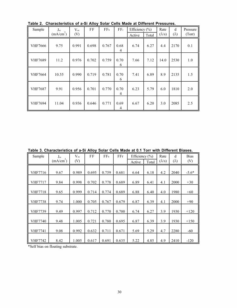
2. Cha ra ct er is ti cs of a- Si Al l oy So la r Cel l s Mad e at Di ff er en t Pr es sur es . 30
3. Cha ra ct er is ti cs of a- Si Al l oy So la r Cel l s Mad e at 0. 1 To rr wi th Di ff er en t Bi as es. 30
4. Cha ra ct er is ti cs of a- Si Ge Al l oy Mi ddl e Cel l s Mad e at Lo wPr es sur e wi th Ex te rn al Bi as . 31
5. Cha ra ct er is ti cs of a- Si Ge Al l oy Mi ddl e Cel l s Mad e at Hi ghPr es sur e wi th Ex te rn al Bi as . 31
6. I ni ti al an d St ab il i zed Cha ra ct er is ti cs of To p Com pon ent Cel l s. 36
7. I ni ti al an d St ab il i zed Cha ra ct er is ti cs of Mi ddl e Com pon ent Cel l s. 36
8. I ni ti al an d St ab il i zed Cha ra ct er is ti cs of Bo tt om Com pon ent Cel l s. 37
9. Av er age Res ul t s of Sma ll - are a a- Si Al l oy To p Cel l s on a 2" x2 "St ai nl es s St ee l Su bst r at e. 40
10 . Av er age Res ul t s of Sma ll - are a a- Si Ge Al l oy Mi ddl e Cel l s on a 2" x2 "St ai nl es s St ee l Su bst r at e. 41
11 . Av er age Res ul t s of Sma ll - are a a- Si Ge Al l oy Bo tt om Cel l s on a 2" x2 "Ag / Zn O Su bst r at e. 42
12 . Av er age Res ul t s of Sma ll - are a Tr ip le -j un ct io n Cel l s on a 2" x2 "Ag / Zn O Ba ck Ref l ec to r. 42
13 . Su mmar y of I ni ti al I -V Cha ra ct er is ti cs of Two Se ts of Ba re Mi ni -Mo dul es . 48
14 . Su mmar y of I ni ti al I -V Cha ra ct er is ti cs of En cap sul at ed Mi ni -Mo dul es . 50
15 . Sp ir e Res ul t s of Li gh t So ak of Fo ur Mi ni -Mo dul es . 50
16 . I ni ti al an d St ab le Sp ir e Res ul t s of En cap sul at ed Mod ul es of Ap ert ur eAr ea ~4 60 cm2. 52
17 . I ni ti al an d St ab le Sp ir e Res ul t s of En cap sul at ed Mod ul es of Ap ert ur eAr ea ~9 20 cm2. 54
vii
Pa ge
18 . Com par is on of Mod ul e Pe rf or manc e at Uni t ed So la r, NRE L, an d Sa ndi aNat i ona l La bor at or y. 56
19 . Ea rl ie r an d Rec en t Sp ir e Mea sur eme nt s at Uni t ed So la r an d NRE Lof Ol d an d New Mod ul es. 58
20 . Su mmar y of Al l St ab le Res ul t s an d Cor r esp ond in g Ph ase I Mi le st one s. 60
1
Executive Summary
Objectives
The principal objective of this R&D program is to expand, enhance and accelerate knowledge andcapabilit ies for the development of high-performance, two-terminal multijunction hydrogenatedamorphous silicon alloy cells and modules with low manufacturing cost and high reliability. Theprogram goal is to obtain 12% stable modules that will qualify IEEE-Std 1262-1995 reliability testing.
Approach
In order to improve efficiency, United Solar uses a spectral-splitting, triple-junction cell structure. Inthis configuration, the top cell uses an amorphous silicon alloy of ~1.8 eV bandgap to absorb the bluephotons. The middle cell uses an amorphous silicon germanium alloy (~20% germanium) of ~1.6 eVbandgap to capture the green photons. The bottom cell has ~40% germanium to reduce the bandgap to~1.4 eV to capture the red photons. The cells are deposited on stainless steel with a predepositedsilver/zinc oxide back reflector to facilitate light trapping. A thin layer of antireflection coating isapplied to the top of the cell to reduce reflection loss.
During this year, research activities were carried out in the following four areas: 1) fundamental studiesto improve our understanding of materials and devices, 2) small-area cell research to obtain the highestcell efficiency, 3) deposition of small-area cells using a modified very high frequency (MVHF)technique to obtain higher deposition rates, and 4) large-area cell research to obtain the highest moduleefficiency.
Status/Accomplishments
1. Fundamental Studies
We have shown previously that hydrogen dilution plays a very important role in improving materialand cell performance. The highest efficiency cells are obtained when the intrinsic material is depositedat a level of hydrogen dilution that is at the threshold between amorphous and microcrystallinetransition. Collaborating with the Colorado School of Mines, we have now demonstrated that thestructural order in this material is determined by the substrate on which the film is grown and also thefilm thickness. The order improves as the thickness increases. This results in the improvement ofmaterial quality in the direction of film growth and has been confirmed by the measurement of defectdensity at the University of Oregon.
2. Small-area Cell Research
We have worked on improving the component cells of the multijunction structure by changing thedeposition conditions. The highest efficiencies obtained in the multijunction structure are given below.
• Achieved 14.4% initial and 12.4% stable active-area (~0.25 cm2) cell efficiency in a dual-bandgap, double-junction structure.
• Achieved 15.2% initial active-area (~0.25 cm2) cell efficiency in a triple-junction structure.
2
3. Cells Deposited at High Rates
We have previously shown that deposition at high rates results in poorer cell performance and stability. This was attributed to a poor microstructure of the film growth at high rates. Since the characteristic ofthe plasma can influence the film property significantly, we have carried out experiments to determinethe energy distribution of the ionized species in the plasma excited by both radio frequency and very highfrequency power sources. The energy of the positive ions is found to increase as the pressure is lowered. The following results have been obtained by using deposition rates of ~3-5 Å /s:
• Deposited single-junction top cells (~0.25 cm2) on stainless steel substrates without backreflector using a-Si alloy at 3-5 Å /s and achieved a total-area stabilized cell efficiency of 4.85%measured under global AM1.5 after 1000 hours of one-sun light soaking at 50 oC.
• Deposited single-junction middle cells (~0.25 cm2) on stainless steel substrates without backreflector using a-SiGe alloy at 3-5 Å /s and achieved a total-area stabilized power output of2.73 mW/cm2 measured under global AM1.5 with a λ>530 nm filter after 1240 hours of one-sun light soaking with an appropriate filter at 50 oC.
• Deposited single-junction bottom cells (~0.25 cm2) on optimized back reflector using a-SiGealloy at 3-5 Å /s and achieved a total-area stabilized power output of 3.11 mW/cm2 measuredunder global AM1.5 with a λ>630 nm filter after 1043 hours of one-sun light soaking with anappropriate filter at 50 oC.
4. Large-area Module Research
Uniformity in deposition over a large area is key to the achievement of high module efficiency. Weuse a large-area reactor where the component cells are deposited over one-square-foot area and theuniformity is investigated by evaluating the performance of small-area cells deposited over the entirearea. Using this method, we have made high efficiency component cells and have fabricated large-area,triple-junction modules. The highlights of this activity are given below:
• Deposited array of single-junction top cells (~0.268 cm2) on stainless steel substrates withoutback reflector using a-Si alloy over areas greater than 900 cm2 and achieved an average total-area stabilized cell efficiency measured under global AM1.5 of 5.4% after 1031 hours of one-sun light soaking at 50 oC.
• Deposited array of single-junction middle cells (~0.268 cm2) on stainless steel substrateswithout back reflector using a-SiGe alloy over areas greater than 900 cm2 and achieved anaverage total-area stabilized power output measured under global AM1.5 with λ>530 nm filterof 3.6 mW/cm2 after 1072 hours of one-sun light soaking with an appropriate filter at 50 oC.
• Deposited array of single-junction bottom cells (~0.268 cm2) on optimized back reflectorsubstrates using a-SiGe alloy over areas greater than 900 cm2 and achieved an average total-areastabilized power output measured under global AM1.5 with λ>630 nm filter of 3.17 mW/cm2
after 621 hours of one-sun light soaking with an appropriate filter at 50 oC.
• Deposited array of triple-junction cells (~0.268 cm2) on optimized back reflector substratesusing optimized component cells over areas greater than 900 cm2 and achieved an averagetotal-area stabilized efficiency measured under global AM1.5 of 11.6% after 1067 hours of one-sun light soaking at 50 oC.
• Achieved 10.5% stable aperture-area (~905 cm2) efficiency in an encapsulated triple-junction
3
module after 1000 hours of one-sun light soaking at 50 oC carried out and measured by NREL.
• Fabricated and delivered two large-area prototype modules with a total area of 216" x 29.6" and216" x 15.5" to NREL; the initial power outputs for the two modules are 317.8 W and 155.5W, respectively, measured at NREL.
Major Publications
1. Guha, S.; Yang, J.; Banerjee, A.; Sugiyama, S. (1998). “Material issues in the commercializationof amorphous silicon alloy thin-film photovoltaic technology.” Mater. Res. Soc. Symp. Proc.;Vol. 507, p. 99.
2. Yang, J.; Sugiyama, S.; Guha, S. (1998). “Effect of excitation frequency on the performance ofamorphous silicon alloy solar cells.” Mater. Res. Soc. Symp. Proc.; Vol. 507, p. 157.
3. Chen, C.C.; Lubianiker, Y.; Cohen, J.D.; Yang, J.; Guha, S.; Wickboldt, P.; Paul, W. (1998). “The electronic structure, metastability and transport properties of optimized amorphoussilicon-germanium alloys.” Mater. Res. Soc. Symp. Proc.; Vol. 507, p. 769.
4. Mahan, A.H.; Reedy, R.C., Jr.; Iwaniczko, E.; Wang, Q.; Nelson, B.P.; Xu, Y.; Gallagher, A.C.;Branz, H.M.; Crandall, R.S.; Yang, J.; Guha, S. (1998). “H out-diffusion and deviceperformance in n-i-p solar cells utilizing high temperature hot wire a-Si:H i-layers.” Mater.Res. Soc. Symp. Proc.; Vol. 507, p. 119.
5. Jiang, L.; Schiff, E.; Wang, Q.; Guha, S.; Yang, J. (1998). "Grazing incidence measurements ofpolarized electroabsorption and light soaking effect on amorphous silicon based solar cells." Mater. Res. Soc. Symp. Proc.; Vol. 507, p. 631.
6. Yang, J.; Banerjee, A.; Lord, K.; Guha, S. (1998). “Correlation of component cells with highefficiency amorphous silicon alloy triple-junction solar cells and modules.” 2nd WorldConference and Exhibition on Photovoltaic Solar Energy Conversion Proceedings; p. 387.
7. Guha, S.; Yang, J.; Banerjee, A.; Hoffman, K.; Call, J. (1998). “Manufacturing issues for largevolume production of amorphous silicon alloy photovoltaic modules.” NCPV PhotovoltaicsProgram Review Proceedings; p. 88.
8. Jiang, L.; Wang, Q.; Schiff, E.; Guha, S.; Yang, J. (1998). "Polarized electroabsorption spectraand light soaking of solar cells based on hydrogenated amorphous silicon." Appl. Phys. Lett.;Vol. 72, p. 1060.
9. Chen, C.; Zhong, F.; Cohen, J.D.; Yang, J.; Guha, S. (1998). "Evidence for charged defects inintrinsic glow-discharge hydrogenated amorphous silicon-germanium alloys." Phys Rev. B; Vol.57 Rapid Communications, p. 4210.
10. Guha, S.; Yang, J.; Williamson, D.L.; Lubianiker, Y.; Cohen, J.D.; Mahan, A.H. (1999). "Structural, defect, and device behavior of hydrogenated amorphous Si near and above the onsetof microcrystallinity." Appl. Phys. Lett.; Vol. 74, p. 1860.
4
Section 1
Introduction
This report describes the research performed during Phase I of a three-phase, three-year program underNREL Subcontract No. ZAK-8-17619-09. The research program is intended to expand, enhance andaccelerate knowledge and capabilit ies for the development of high-performance, two-terminalmultijunction amorphous silicon (a-Si) alloy cells and modules with low manufacturing cost and highreliability.
In order to improve efficiency, United Solar uses a spectral-splitting, triple-junction cell structure. Inthis configuration, the top cell uses an amorphous silicon alloy of ~1.8 eV bandgap to absorb the bluephotons. The middle cell uses an amorphous silicon germanium alloy (~20% germanium) of ~1.6 eVbandgap to capture the green photons. The bottom cell has ~40% germanium to reduce the bandgap to~1.4 eV to capture the red photons. The cells are deposited on stainless steel with a predepositedsilver/zinc oxide back reflector to facilitate light trapping. A thin layer of antireflection coating isapplied to the top of the cell to reduce reflection loss.
During this year, research activities were carried out in the following four areas: 1) fundamental studiesto improve our understanding of materials and devices, 2) small-area cell research to obtain the highestcell efficiency, 3) deposition of small-area cells using a modified very high frequency (MVHF)technique to obtain higher deposition rates, and 4) large-area cell research to obtain the highest moduleefficiency. Results on 1) and 2) are described in Section 2. Data on higher deposition rates are given inSection 3. Module research activities are detailed in Section 4. Section 5 gives future directions.
5
Section 2
Amorphous Silicon Alloy Materials and Solar Cells Near the Threshold of Microcrystallinity
Introduction
Over the last two decades, photovoltaic (PV) technology using amorphous silicon (a-Si) alloy materialshas advanced significantly to a stage where large-scale manufacturing is taking place worldwide (Rannels1998). Most of the products to date are aimed at terrestrial applications such as battery charging andbuilding-integrated photovoltaics. On the other hand, due to the tremendous growth in the field oftelecommunication, intensive efforts are underway to qualify the lightweight inexpensive thin-filmsolar cells for space applications (Guha et al. 1998). Today, state-of-the-art a-Si alloy triple-junctionmodules on thin, flexible substrates are being seriously evaluated in orbit such as those from UnitedSolar Systems Corp. (United Solar) on board the MIR space station.
Despite the substantial progress made in recent years, the biggest challenge for both terrestrial andextraterrestrial applications today is achieving even higher conversion efficiencies. A National Thin-film Partnership Team including members from the PV industry, universities, and national laboratorieswas organized in 1992 by the National Renewable Energy Laboratory (NREL) to coordinate andaddress various aspects of the thin-film materials and devices (von Roedern et al. 1997). A broadspectrum of activities, ranging from fundamental material studies to novel multijunction designs, hasbeen addressed. In the last several years, the most important finding from these activities forimproving stabilized cell efficiencies using plasma-enhanced chemical vapor deposition (PECVD) isprobably the realization of the benefit of using hydrogen dilution during film growth (Yang et al. 1994). Although the first report on the effect of hydrogen dilution was made in 1981 by Guha et al. (Guha etal. 1981), it was not until the 1990's that improvement on solar cell performance using this approachbecame available in the literature. These cells exhibit higher efficiencies and better light stability.
A recent study by Tsu et al. (Tsu et al. 1997) further revealed that a-Si alloy materials grown usingappropriate hydrogen dilution result in more-ordered microstructures in that intermediate-range ordershave been observed. As the hydrogen dilution ratio is increased, there exists a transitional regionbeyond which microcrystallites begin to form rapidly. The best quality a-Si alloy solar cells areobtained when one deposits the material just below the threshold of the amorphous to microcrystallinetransition. In this section, we review some interesting features associated with the materials near thethreshold and discuss the corresponding solar cell performance.
Experimental Results and Discussion
Near Threshold M aterial Characteristics
The first experimental observation of improved stability against light soaking by using hydrogendilution during film growth was reported by Guha at al. in 1981 (Guha et al. 1981). They found thatfilms obtained using 10% silane (SiH4) and 90% hydrogen (H2) exhibited better stability than thosegrown using 100% SiH4.
6
In 1994, we reported that a-Si alloy solar cells whose intrinsic layers were made with high hydrogendilution displayed better stability than those made with low dilution at a same deposition temperature of300 oC (Yang et al. 1994). In order to understand the difference in the two types of materials, wemeasured film properties such as infrared (IR) absorption, optical bandgap, hydrogen evolution, andsmall-angle X-ray scattering (SAXS). From the IR absorption spectra and optical bandgapmeasurements, we found that both types of materials contain ~10% of bonded hydrogen, and theiroptical bandgaps around 1.72 eV are also similar. On the other hand, the hydrogen evolution spectrafor the two types of materials are distinctly different, as shown in Fig. 1. The low dilution sampleexhibited a broad evolution peak near 500 oC (Fig. 1(a)), while the high dilution sample displayed asharp, narrow peak near 400 oC (Fig. 1(b)) (Xu et al. 1996). This pronounced difference suggests thatthe microstructure of the two types of films may be quite different. Based on the IR analyses, it waspointed out that the low temperature evolution peak was not associated with dihydride or polyhydridestructures. In addition, SAXS data showed that high hydrogen dilution samples contain orientedmicrostructures parallel to the film growth direction (Jones et al. 1993, Williamson 1995). Based onhydrogen evolution and SAXS data, it appears that the high dilution samples may have a heterogeneousstructure.
Furthermore, we have made a-Si alloy solar cells using a gas mixture of SiD4 and D2 and compared thecell performance to those obtained from SiH4 and H2. We found that, using similar depositionconditions and intrinsic layer thicknesses, the deuterated cells show better stability against light soakingthan the hydrogenated counterparts (Sugiyama et al. 1997). What is also interesting is that thedeuterium evolution spectrum also showed a sharp, low temperature peak near 400 oC, displayed in Fig.2.
From the above experimental results, it appears that the deposition conditions used for achieving morestable solar cells also lead to materials having a low temperature peak in the evolution spectra. Abetter stability seems to be correlated with an improved microstructure.
In order to further investigate the correlation between enhanced stability and the effect of hydrogendilution, we collaborated with Tsu et al. (Tsu et al. 1997) and carried out a systematic study on samplesprepared with low, medium, and high hydrogen dilutions. We used high resolution transmission electronmicroscopy (TEM) and Raman scattering measurements to look for qualitative and quantitativedifferences in the three types of films. Figure 3 shows the Raman spectra for a-Si alloy films of ~500Å thick deposited on 7059 Corning glass. The low, medium, and high dilution films are shown in Fig.3(b), 3(c), and 3(d), respectively. Also shown in Fig. 3(a) is a standard a-Si alloy film prepared with nohydrogen dilution. The following two observations are made. First of all, there is a shift in the Si TOpeak position, indicated by the dashed line, from no dilution to high dilution. Secondly, a sharp bandappeared at 516.5 cm-1 for the high dilution sample (Fig. 3(d)), and is attributed to microcrystallineinclusions. From this study, a clear trend emerges in that as the hydrogen dilution increases, itpromotes the formation of microcrystallites in the amorphous matrix.
The films were subsequently lifted off the 7059 glass substrates and their microstructures analyzed byTEM. For the high dilution sample, distinct microcrystallites were indeed observed embedded in thefeatureless amorphous matrix even under low magnification. These spherical microcrystallites have sizesranging from 2 to 10 nm in diameter. Under high magnification, TEM micrograph revealed that the highdilution sample exhibited long parallel lines separated by 0.31 nm, corresponding to the d spacing of Si(111) planes. In addition, one-dimensional linear-like objects that appear to have some degree of orderalong the length were observed. These objects have widths of 2-3 nm and lengths of up to a few 10's ofnm. In fact, a careful examination of the other three samples showed that they all contain, to a lesserdegree, these linear-like objects. This is true even for the standard sample prepared with no hydrogendilution. Based on TEM and Raman data, we conclude that the intermediate range order of different
7
Figure 1. Hydrogen evolution spectra for (a) the low dilution and (b) the high dilution samples.
0
2
4
6
8
300 400 500 600 700
Temperature (OC)
dP/d
T (
a.u.
)b) High Hydrogen
Dilution
a) Low Hydrogen Dilution
8
Figure 2. Deuterium evolution spectrum from the deuterated sample.
0
2
4
6
8
300 400 500 600 700
Temperature (OC)
dP/d
T (
a.u.
) SiD4+D2
9
Figure 3. Raman spectra versus hydrogen dilution of four samples: (a) no dilution, (b) lowdilution, (c) medium dilution, and (d) high dilution.
10
degrees indeed exists in a-Si alloy films. The volume fraction occupied by microcrystallites within theamorphous material increases with increasing hydrogen dilution.
Recently, we have conducted a series of X-ray diffraction (XRD) studies on a-Si alloys prepared fromvarious hydrogen dilutions to see if XRD signals can be correlated with hydrogen dilution ratios (Guhaet al. 1999). We found that the full-width-at-half maximum (FWHM) intensity of the first X-raydiffraction peak is narrower in high hydrogen diluted samples than those in low or no hydrogen dilutionsamples. This confirms the improved medium range order for high dilution samples. A detailedaccount is given by Williamson (Williamson 1999).
Very recently, in collaboration with Mahan et al., we carried out systematic IR and H2 evolution studiesfor hydrogen diluted samples. A careful analysis of the IR spectra revealed that the peak frequency ofthe Si-H wagging mode shifts downward from ~640 cm-1 to 620 cm-1 for high H2 dilution. The 620 cm-
1 frequency has been interpreted as being due to H bonded to the surfaces of very small, highly eccentricSi microcrystallites. These crystallites catalyze the crystallization of the remainder of the amorphousmatrix upon annealing and resulting in the observed low temperature peak in the H2 evolutionspectrum. A more detailed description of this work is given by Mahan et al. (Mahan et al. 1999).
Kamei et al. (Kamei et al. 1999) recently investigated effects of embedded crystallites in hydrogenatedamorphous silicon on light-induced metastable dangling bond defect creation. The crystalline-likenanostructures were obtained by using hydrogen dilution during film growth, confirming the observationby Tsu et al. (Tsu et al. 1997). They also found that inclusion of a small-volume fraction ofcrystallites into the amorphous matrix significantly suppresses defect creation against moderate lightillumination. They propose that the mechanism of improved stability is related to thetrapping/recombination of photocarriers by embedded crystallites.
From the above discussion, it should be clear that appropriate hydrogen dilution can create intermediaterange order and improve material properties. However, dilution beyond certain critical value oftenresults in excess microcrystallite inclusions and degrades solar cell performance. In fact, a-Si alloy p i ncells with excess hydrogen dilution give rise to low open-circuit voltages and poor cell performance. We should also point out that the threshold condition is system dependent. In one system, a dilutionratio of ten to one may be the optimum, while in a different system, one may need a very differentratio. Other deposition parameters, such as pressure, temperature, electrode spacing, chambergeometry, and gas flows, all affect the growth kinetics. In fact, conditions too close to the thresholdmay not be easily reproducible. They may be too sensitive to small variations in the depositionconditions, as shown by a recent work using real-time spectroscopic ellipsometry (Koh et al. 1998).
Near Threshold Solar Cell Performance
From the above discussion, one should recognize the importance of using appropriate hydrogen dilutionin the PECVD process to optimize the deposition conditions so that high quality materials can beobtained near the amorphous to microcrystalline transition. We have followed this approach and studiedfour different types of solar cell structures shown in Fig. 4. These structures use stainless steel substratesand textured silver/zinc oxide as back reflectors. Figure 4(a) shows the basic p i n structure mostcommonly used to evaluate the quality of the a-Si alloy materials. To achieve high efficiency in thisstructure, not only does one need high quality intrinsic material such as those discussed above, but alsoother key requirements such as light trapping, transparent conductive oxide, and interface properties. The thickness of the intrinsic layer is also very important. If the intrinsic layer is too thick, cells willsuffer large degradation due to the Staebler-Wronski effect (SWE) (Staebler et al. 1977). If the intrinsiclayer is too thin, it does not absorb sufficient photons, thus resulting in low efficiencies. An optimum
11
Figure 4. Schematic diagram of four solar cell structures: (a) single, (b) same bandgap, double,(c) dual bandgap double and (d) triple junctions.
ITOp
i a-Si alloy
np
i a-Si alloy
nZinc Oxide
Silver
Stainless Steel
ITOp
i a-Si alloy
np
i a-SiGe alloy
nZinc Oxide
Silver
Stainless Steel
ITOp
i a-Si alloynp
i a-SiGe alloynp
i a-SiGe alloyn
Zinc OxideSilver
Stainless Steel
ITOp
i a-Si alloy
nZinc Oxide
Silver
Stainless Steel
Grid
(a) Single - Junction (b) Same GapDouble - Junction
(c) Dual GapDouble - Junction
(d) Triple - Junctio
Grid Grid Grid
12
thickness of ~2200 Å was used to achieve the highest stabilized active-area efficiency of 9.3%. Theinitial and stable J-V characteristics are listed in Table 1. It should be pointed out that the degradationdue to SWE for this structure is only 12.3%, a value much lower than the typical 50% degradationwhen the quality of the material was poor or the thickness of the intrinsic layer was too thick. Usinghydrogen dilution during deposition, one generally observes less degradation and an earlier saturation(Yang et al. 1994, Yang et al. 1994).
For the same bandgap double-junction structure shown in Fig. 4(b), one takes advantage of the thin topcell. The thin top cell gives rise to a high internal field (Jiang et al. 1996), thus less degradation. Thetop cell also absorbs the high energy photons and allows only low energy photons to reach the bottomcell. From Table 1, we see that the initial fill factor of the same bandgap structure is higher than thesingle-junction structure; the stabilized fill factor is also higher. The stabilized efficiency of 10.1% isbetter than the 9.3% obtained from the single-junction structure.
In order to further increase the cell efficiency, one resorts to narrow bandgap materials such as a-SiGealloys to broaden the spectral response. The carrier transport properties in the a-SiGe alloy materials,however, are often worse than those in the a-Si alloys. Using the hydrogen dilution approach, we havebeen able to improve the performance of the a-SiGe alloy solar cells substantially. Hydrogen dilutionalso allows for a lower deposition temperature without deteriorating the fill factor of the device (Shimaet al. 1997). Figure 5 shows the J-V characteristic of an improved a-SiGe alloy device having anaverage germanium concentration of ~20% in the intrinsic layer. The intrinsic layer has alsoincorporated a bandgap profiling design (Guha et al. 1989) to improve the cell performance. The11.6% initial active-area efficiency is the highest reported to date for a single-junction a-SiGe alloysolar cell.
Table 1. Highest Stable Cell Efficiencies (active area ~0.25 cm2)
at United Solar for Different Junction Configurations.
Figure 5. Initial J-V characteristic of an a-SiGe alloy p-i-n solar cell.
-25.0
-20.0
-15.0
-10.0
-5.0
0.0
5.0
-0.2 0.0 0.2 0.4 0.6 0.8
Volts (V)
J (m
A/c
m2 ) Voc=0.790 V
Jsc=21.89 mA/cm2
FF=0.670Eff=11.6%
A=0.25 cm2
14
Using the improved a-SiGe alloy in the bottom cell, we then proceeded to make dual bandgap double-junction solar cells using the structure shown in Fig. 4(c). In this structure, the top cell needs to bethicker than that of the same gap structure in order to match the higher photocurrent generated by thea-SiGe alloy bottom cell. The initial and stable characteristics of the best dual gap double-junction cellis also shown in Table 1. Comparing the dual gap and same gap structures, it is obvious that the mainadvantage of the dual gap structure is the substantially higher current density, which overcomes thelower open-circuit voltage and fill factor. In fact, the dual gap structure shows a more than 20% gain inthe stabilized efficiency than the same gap structure. The degradation of the dual gap device, on theother hand, is higher than the same gap counterpart. This is mainly due to the thicker top cell and thesomewhat poorer a-SiGe alloy material in the bottom cell.
To further enhance the efficiency and broaden the spectral response, we next discuss the triple-junctionconfiguration shown in Fig. 4(d). The structure incorporates a low bandgap a-SiGe alloy in the bottomcell. In this configuration, the bandgap and thickness of the top and middle cells are dictated by thequality of the bottom cell. If one can successfully incorporate a higher concentration of germaniuminto the bottom cell and further extend the spectral response into the long wavelength region, one maysplit the spectral response into blue, green, and red regions, corresponding to the top, middle, andbottom cells, respectively. The goal of this design is, of course, that the gain in current can overcomethe loss in Voc and FF. We have again used the hydrogen dilution method and successfully achieved14.6% initial and 13.0% stable conversion efficiencies for a 0.25 cm2 active-area device in the triple-junction configuration. Their J-V characteristics are also listed in Table 1. Figure 6 shows the J-Vcharacteristic of the 14.6% triple-junction cell; the quantum efficiency versus wavelength plot for thisdevice is shown in Fig. 7.
It should be pointed out that the stabilized efficiency for each structure in Table 1 represents thehighest value reported to date in the literature. Hydrogen dilution indeed played a major role inachieving this result . We should also point out, however, that high quality material is a necessary butnot sufficient condition for making high efficiency solar cells. Other key factors, such as the design ofthe device structure, the appropriate back reflector, the thickness and the optical bandgap of theintrinsic layer, the bandgap profiling of the a-SiGe alloys, the interface layers, the tunnel junctions, thecomponent cell current matching, and the top conductive oxide, all play an important role in achievingthe high efficiency cells (Yang et al. 1997).
Based on the experimental data of Table 1, it is easy to conclude that the triple-junction structure givesrise to the highest initial and stable efficiencies. The quantum efficiency curve in Fig. 7 clearly showsthe spectral-splitting feature of the triple-junction design. The current mismatch observed among thethree component cells is designed to limit the triple-junction current by the top cell which usually hasthe best fill factor. Any improvement in the fill factor of the middle or bottom cell can allow us tofurther reduce the current mismatch and improve the cell efficiency. Our continuous effort inoptimizing the device design and deposition conditions has led us to achieve a 15.2% initial active-areaefficiency. The J-V characteristic is shown in Fig. 8, and the quantum efficiency plot is shown in Fig.9. From Fig. 9, one can see that the spectral response spans from below 350 nm to beyond 950 nmwith the peak quantum efficiency exceeding 90% in the green region. The triple stack generates a totalphotocurrent of 27 mA/cm2. The current mismatch among the component cells has been virtuallyeliminated.
Based on the above experimental results and discussion, it is clear that hydrogen dilution improves themicrostructure and enhances the cell performance. The optimum condition is very close to theamorphous to microcrystalline transition. The challenge is to approach the threshold withoutexceeding the critical limit. In order to find out the cell characteristics at optimum conditions, we haveevaluated a series of a-Si alloy top cells on stainless steel substrates by adjusting the hydrogen dilution
15
Figure 6. Initial J-V characteristic of the 14.6% triple-junction cell.
-10.0
-7.5
-5.0
-2.5
0.0
2.5
-0.5 0 0.5 1 1.5 2 2.5
Volts (V)
J (m
A/c
m2 ) Voc=2.357 V
Jsc=8.57 mA/cm2
FF=0.723Eff=14.6%
A=0.25 cm2
16
Figure 7. Quantum efficiency of the device shown in Fig. 6.
0.0
0.2
0.4
0.6
0.8
1.0
350 450 550 650 750 850 950Wavelength (nm)
Qua
ntum
Effi
cien
cy 26.88
mA/cm2
8.57 9.01 9.30
17
Figure 8. Initial J-V characteristic of the 15.2% triple-junction cell.
-10.0
-7.5
-5.0
-2.5
0.0
2.5
-0.5 0.0 0.5 1.0 1.5 2.0 2.5
Volts (V)
J (m
A/c
m2 )
Voc=2.344 V
Jsc=8.99 mA/cm2
FF=0.722Eff=15.2%
A=0.25 cm2
18
Figure 9. Quantum efficiency of the device shown in Fig. 8.
0.0
0.2
0.4
0.6
0.8
1.0
350 450 550 650 750 850 950
Wavelength (nm)
Qua
ntum
Effi
cien
cy
9.15 8.99
27.16
mA/cm2
9.02
19
condition near the threshold. The requirement is that the Jsc value must be around 8 mA/cm2 for topcell applications. Figure 10 shows the best cell obtained to date in terms of high fill factor and highopen-circuit voltage. The cell exhibits FF = 0.785, Voc = 1.010 volt, and Jsc = 8.25 mA/cm2. As soonas the dilution ratio exceeds a certain critical value, a sudden drop in FF and Voc occurs, signifying thatthe threshold has been exceeded.
Hydrogen dilution in general lowers the deposition rate. The high efficiency cells described above havea typical deposition rate of ~1 Å/s. Can one obtain high quality materials and solar cells using highdeposition rates? This is of particular interest concerning the throughput in large volume productions. We have used a modified very high frequency (MVHF) approach and studied the hydrogen dilutioneffect on high-rate-deposited top cells (Yang et al. 1998). More detail is discussed in Section 3. Figure11 shows the best cell obtained to date using MVHF with hydrogen dilution at a deposition rate of 8 Å/s. The J-V characteristic is very close to that of the 1 Å /s cell shown in Fig. 10. High performance a-Si alloy cells can indeed be achieved at high rates using an appropriate hydrogen dilution. More work isneeded to study the a-SiGe alloy using high deposition rates.
Summary
Using hydrogen dilution during film growth in the PECVD process, we have shown that themicrostructure of the material and solar cell performance are improved. Interesting features associatedwith hydrogen diluted films near the amorphous to microcrystalline transition are reviewed. Theyinclude the observation of linear-like objects in the TEM micrograph, a shift of the principal Si TOband in the Raman spectrum, a low temperature H2 evolution peak, a shift in the wagging modefrequency in the IR spectrum, and a narrowing of the Si (111) peak in the X-ray diffraction pattern.
World record high efficiency solar cells in four different device structures have been achieved byoptimizing hydrogen dilution conditions near the threshold of the amorphous to microcrystallinetransition. More work is needed to understand these hydrogen diluted materials to improve theefficiencies further.
20
Figure 10. Initial J-V characteristic of an a-Si alloy top cell deposited at ~1 Å/s.
-10
-8
-6
-4
-2
0
2
-0.25 0.25 0.75 1.25
Voltage (V)
J (m
A/c
m2 )
Voc=1.010 V
Jsc=8.25 mA/cm2
FF=0.785Eff.=6.54%
A=0.25 cm2
21
Figure 11. Initial J-V characteristic of an a-Si alloy top cell deposited at ~8 Å/s by MVHF.
-10
-8
-6
-4
-2
0
2
-0.25 0.25 0.75 1.25
Voltage (V)
J (m
A/c
m2 )
Voc=0.995 V
Jsc=8.34 mA/cm2
FF=0.749Eff.=6.22%
A=0.25 cm2
22
Section 3
Status of Small Area Component and Multi-junction CellsDeposited with RF and MVHF at 3~5 Å/s
Introduction
Investigations are underway to increase the stabilized total area efficiency of triple-junction solarcells deposited at both high rate, 3 - 5 Å/s, and low rate, 1 Å/s. Higher deposition rates are attractivebecause of increased throughput and reduced manufacturing costs. To achieve higher depositionrates, both RF (13.56 MHz) and MVHF (75 MHz) PECVD are being investigated. In an earlier study,we have shown that an increase in the deposition rate of a-Si alloys using 13.56 MHz resulted in anincrease in microvoid density, which is believed to cause a poorer cell performance and stability(Guha et al. 1992). On the other hand, we have also found that the microstructure of the materialdepends critically on the deposition conditions such as the degree of hydrogen dilution during the filmgrowth (Tsu et al. 1997). Moreover, solar cells made using a 2.45 GHz microwave excitation with adeposition rate of ~100 Å/s have given high initial efficiencies (Guha et al. 1995). An optimumdeposition condition for high quality materials may exist for a given excitation frequency. Currently, the highest stabilized efficiencies are deposited with a conventional RF-PECVD at rate of1 Å/s. Initial and stabilized active area efficiencies of 14.6% and 13.0% have been reported (Yang etal. 1997). The initial performance of single-junction a-Si alloy cells fabricated by MVHF at 6 Å/s issimilar to RF at 3 Å/s. However, the stability of a-Si alloy MVHF cells is superior to the 3 Å/s RFtop cells. High deposition rate a-SiGe alloy middle cells fabricated with RF and MVHF exhibit similarcharacteristics. MVHF bottom cells currently exhibit inferior initial and stabilized performance thanthe RF bottom cells. Experiments are being conducted to identify the source of the deficit in theMVHF bottoms cells deposited faster than 3 Å/s and are discussed in detail below.
Status of 3 Å/s RF a-Si Alloy Solar Cells
Efforts are being made to increase the total area efficiencies of the single-junction component cellsdeposited by 13.56 MHz RF at 3Å/s. The small area cells have a total area of 0.268 cm2 and anactive area of 0.25 cm2. Top and middle component cells are deposited on bare stainless steel. Bottom cells are deposited onto a textured AgZnO back reflector. Top cells are measured underAM1.5 illumination. Middle cells are measured under AM1.5 illumination with a 530 nm cut onfilter, and bottom cells are measured with a 630 nm cut on filter. A stabilized total area efficiency of4.70% has been reported for the top cell and meets the Phase I goal. A stabilized total area pmax of2.80 mW/cm2 for the middle cell and 3.20 mW/cm2 for the bottom cell have also been previouslyreported. In the course of this phase, middle cell B4410 with an initial total area pmax of 3.91mW/cm2, and stabilized pmax of 2.80 mW/cm2 has been fabricated. The bottom cell, B4030, with aninitial total area pmax of 3.80 mW/cm2 and a stabilized pmax of 3.11 mW/cm2 has been fabricated, andmeets the Phase I goal.
The characteristics of triple-junction a-Si alloy cells deposited by RF at 3 Å/s are reported. B3363, atriple-junction cell, has an initial AM1.5 total area efficiency of 11.7% and a stabilized total areaefficiency of 9.5%. The stabilized efficiency is to be improved to 10.7% to meet the proposedPhase I goal. Currently, the single-junction top and bottom component cells meet the proposedstabilized total area Phase I goal of 4.7% and 3.0 mW/cm2, respectively. However, the middle andtriple-junction cells are to be improved. Investigations are underway to reduce the degradation in themiddle cell.
23
Modified Very-High-Frequency Plasma Enhanced Chemical Vapor Deposition(MVHF-PECVD): Plasma Properties and Solar Cell Deposition
Introduction
Ten years ago, Chatham and Bhat (Chatham et al. 1989) used very-high-frequency (VHF) PECVD todeposit a-Si alloy solar cells at high deposition rates. They demonstrated an efficiency of 9.7% for an a-Si alloy solar cell made at 18 Å/s using a frequency of 110 MHz. Since then, many groups have used thistechnique to deposit a-Si alloy materials and devices. The group at Utrecht studied the properties of theVHF plasma (Harmers et al. 1997) and deposited a-Si alloy solar cells (Van Spark et al. 1996) and thinfilm transistors. They reached an initial efficiency of 10% (Van Spark et al. 1996). The group atNeuchâtel showed that VHF-PECVD has advantages to make microcrystalline silicon (µc-Si) at ratesmuch higher than ordinary RF plasma deposition of µc-Si (Shah et al. 1997). They deposited µc-Si solarcells and a-Si/µc-Si tandem solar cells.
In our laboratory, we have used an MVHF-PECVD (refer to MVHF) system to deposit a-Si and a-SiGealloy solar cells. We found that a-Si alloy solar cells made with MVHF at 6 Å/s show similar initialperformance as those made with RF at 3 Å/s, and the stability of 6 Å/s MVHF cells is better than the 3Å/s RF cells (Yang et al. 1998). To further improve the performance of the MVHF solar cells made athigh deposition rates, we need to understand the difference in the plasmas excited by RF and MVHF,and search for further improvement of the solar cells. For this purpose we have systematically studiedthe ion energy distribution of MVHF and RF plasmas as well as the effects of ion bombardment on theperformance of a-Si and a-SiGe alloy solar cells. It has been shown that high H2 dilution can improvethe performance and stability of a-Si alloy solar cells made with RF plasmas at low deposition rates(Guha et al. 1981). However, the effect of H2 dilution on the solar cells made with MVHF at high ratesare not clear. Recent studies on the effects of H2 dilution on the a-Si and a-SiGe alloy solar cells aresummarized in the last sub-section.
Experimental
A parallel plate capacitance reaction chamber (MVHF chamber), which was adapted to a multi-chamber PECVD system, was designed to have the capability to couple RF (13.65 MHz) and VHF (75MHz) frequencies to the plasma. The substrate can be grounded, externally biased or floated, whichgives us the flexibility to study the effects of ion bombardments. A retarding field analyzer wasinstalled in the plasma chamber to measure the energy distribution of positive ions. The details ofthe ion energy distribution experiments are presented elsewhere (Yan et al. 1999). The ion energydistributions of H2, Ar, SiH4 and their mixtures were studied as functions of excitation frequency, RFor VHF power density and pressure. a-Si and a-SiGe alloy component cells were made with variousconditions, such as different pressures, gas flow rates, substrate temperatures and external biases, t ooptimize their performance and to improve the tandem and triple junction cells.
Ion energy distribution and the effects of ion bombardments on a-Si alloy solar cells
Figure 12 shows the energy distribution of ions in H2 plasma with 75 MHz excitation, where the VHFpower was 10 W. At a low pressure (0.1 Torr), a sharp peak appears at 22 eV with a full width at half-maximum of about 6 eV. The cut-off at the high energy side is very sharp. This value could be theplasma potential. However, at high pressure (1.0 Torr), the peak of ion energy distribution shifts to zeroand the width becomes significantly broader. Similar measurements were carried out for the RF plasma.Figure 13 shows the results of the RF plasma with the same conditions as in Fig. 12 except the excitation
24
Figure 12. The energy distribution of positive ions reached to the substrate in a H2 plasmaexcited by 75 MHz VHF. The pressures were 0.1 and 1.0 Torr and VHF power was 10 W.
-0.2
0
0.2
0.4
0.6
0.8
1
1.2
-50 -30 -10 10 30 50 70
Vc (V)
-dJ
c/d
Vc
(a
rb.
un
its
)
0.1 torr
1.0 torr
Vs
25
Figure 13. The positive ion energy distribution of a H2 plasma excited by 13.56 MHz RF. Otherconditions are the same as in Fig.12.
-0.02
0
0.02
0.04
0.06
0.08
0.1
-50 -30 -10 10 30 50 70
Vc (V)
-dJ
c/d
Vc
(a
rb.
un
its
)
0.1 TORR
1.0 TORR
Vs
26
frequency was 13.56 MHz. The peak position is much higher (37 eV) than that shown in Fig. 12,and the distribution is also much broader (18 eV). Similar to the MVHF plasma, there are no highenergy ions reaching the substrates at 1.0 Torr. In addition, the positive ion current that reached thesubstrate is about 5 times higher in the 75 MHz MVHF plasma than in the RF plasma.
The shifting and broadening of the ion energy distribution with the increase in pressure could resultfrom the collision of positive ions with neutral species when the ions travel through the sheath. Thecollision not only transfers energy to neutral species but also has a probability to exchange charge. The charge-exchange collision yields low energy neutral radicals and reduces the energy of the ions asmeasured by the retarding field analyzer. This process is significant in Ar plasma since the charge-exchange collision cross section is very large for argon ions (Gallagher 1999). Experimentally, wefound that the ion energy distribution collapsed even at low pressure for Ar plasma (0.1 torr).
Compared with pure H2 plasma, a mixture of SiH4 and H2 shifts the ion energy distribution to a lowerenergy, as shown in Fig. 14. This shift probably indicates that the plasma potential is higher for pureH2 plasma than for the plasma with H2 and SiH4 mixture. This phenomenon is similar for both RFand MVHF plasmas.
The increase of excitation power slightly shifts the energy distribution of MVHF plasma to a higherenergy as shown in Fig. 15. The shape of the ion energy distribution remains unchanged within theexperimental errors. It probably means that the plasma potential is increased by the high powersince the peak-to-peak voltage increases with the increase of power level. However, for a RF plasmathere is no significant change at the cut-off energy, instead the shape of the distribution is changed. Figure 16 compares the ion energy distributions for an RF plasma with 3 W and 30 W. Because theplots are in arbitrary units, we may only say that the ratio of the high energy peak to the broad lowenergy shoulder increases with the increase of RF power. The mechanism responsible for thedifference in the power dependence between RF and MVHF is not clear at this stage.
From the ion energy distribution measurements we have learned the following. First, the ionbombardment occurs only at low pressures. For normal solar cell deposition pressures, there is nosignificant ion bombardment from the plasma itself. Second, at low pressures, the ion bombardmentis higher in RF plasma than in MVHF plasma. Third, the positive ion flux is higher in MVHF plasmathan in RF plasma.
In order to find out whether the ion bombardment is beneficial for making a-Si alloy solar cells withMVHF, we have performed systematic studies of the effects of pressure and external bias on a-Sialloy solar cells. Table 2 lists the characteristics of a-Si alloy solar cells deposited on stainless steelwith a thickness of around 2100 Å, where the intrinsic layers were deposited at different pressures. The deposition rate is significantly influenced by the pressure. The cell made at 0.1 Torr is not asgood as the cells made at 1.0 Torr or 1.5 Torr although the deposition rate is only 4.4 Å /s. This isprobably due to the ion bombardment. On the other hand, at pressures higher than 2.0 Torr, the Voc
and FF drop, which may have resulted from the polymerization in the plasma.
Table 3 summarizes the performance of a-Si alloy solar cells deposited at 0.1 Torr with differentexternal DC biases. The positive and negative biases slightly reduce and enhance the deposition rate,respectively. The FF of the positively biased cells is better than the one deposited on a floatingsubstrate. The negative bias significantly reduces the FF. Physically, a positive bias reduces the energyand flux of the positive ions and a negative bias accelerates the positive ions toward the substrate. Therefore, we may conclude that ion bombardment is not beneficial for making a-Si alloy solar cellsusing our MVHF with current conditions.
27
Figure 14. Comparison of the positive ion energy distribution of pure H2 plasma and plasmawith H2 and SiH4 mixture. The measurements were made at 0.1 torr with 11 W VHF power.
-0.05
0
0.05
0.1
0.15
0.2
0.25
0.3
-50 -30 -10 10 30 50 70
Vc (V)
-dJc
/dV
c (a
rb.
un
its)
H2=121 SCCM,SiH4=0 SCCM
H2=106 SCCM,SiH4=5 SCCM
Vs
28
Figure 15. Ion energy distribution with two VHF powers for a H2 plasma at 0.1 torr.
-0.05
0
0.05
0.1
0.15
0.2
0.25
0.3
-50 -30 -10 10 30 50 70
Vc (V)
-dJ
c/d
Vc
(a
rb.
un
its
)
13.5 W
32.5 W
Vs
29
Figure 16. Ion energy distribution with two RF powers for a H2 plasma at 0.1 torr.
-0.20
0.00
0.20
0.40
0.60
0.80
1.00
1.20
1.40
-50 -30 -10 10 30 50 70
Vc (V)
-dJc
/dV
c (a
rb.
un
its)
30 W
3 W
Vs
30
Table 2. Characteristics of a-Si Alloy Solar Cells Made at Different Pressures.
Efficiency (%)Sample Jsc
(mA/cm2)
Voc
(V)FF FFb FFr
Active Total
Rate(Å/s)
d(Å)
Pressure(Torr)
VHF7666 9.75 0.991 0.698 0.767 0.684
6.74 6.27 4.4 2170 0.1
VHF7689 11.2 0.976 0.702 0.759 0.706
7.66 7.12 14.0 2530 1.0
VHF7664 10.55 0.990 0.719 0.781 0.706
7.41 6.89 8.9 2135 1.5
VHF7687 9.91 0.956 0.701 0.770 0.704
6.23 5.79 6.0 1810 2.0
VHF7694 11.04 0.936 0.646 0.771 0.694
6.67 6.20 3.0 2085 2.5
Table 3. Characteristics of a-Si Alloy Solar Cells Made at 0.1 Torr with Different Biases.
The pressure and external bias experiments were also carried out on a-SiGe alloy middle cells. Theperformance of middle cells is strongly dependent on pressure. The cells made at low pressure (0.1Torr) show relatively poor performance. However, the external bias probably has more effect at lowpressures than at high pressures. Therefore, we first made a-SiGe alloy middle cells at a low pressurewith different biases on the stainless steel substrate. The characteristics of these cells are listed inTable 4, where the measurements were made under an AM1.5 solar simulator with a 530 nm cut-onfilter. The negative bias increases Voc and decreases Jsc, which probably means that less Ge isincorporated into the a-SiGe alloy layer. The positive bias has very little effect on the performanceof the cell. Since our current best a-SiGe alloy cell is made at high pressure, we examine the biaseffect for high pressure cells. The results are listed in Table 5. Similar to the low pressure case, thepositive bias does not affect the cell performance, but the negative bias reduces the FF. It should bepointed out, however, the negatively biased cells are slightly thicker than the unbiased and positivelybiased cells.
Table 4. Characteristics of a-SiGe Alloy Middle Cells Made at Low Pressure with External Bias.
Effects of Hydrogen Dilution on a-Si and a-Si alloy Solar Cells
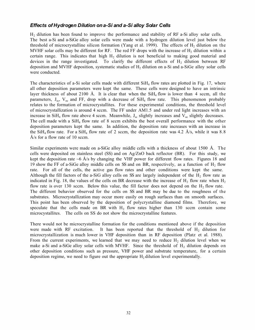
H2 dilution has been found to improve the performance and stability of RF a-Si alloy solar cells. The best a-Si and a-SiGe alloy solar cells were made with a hydrogen dilution level just below thethreshold of microcrystalline silicon formation (Yang et al. 1999). The effects of H2 dilution on theMVHF solar cells may be different for RF. The red FF drops with the increase of H2 dilution within acertain range. This indicates that high H2 dilution is not beneficial to making good material anddevices in the range investigated. To clarify the different effects of H2 dilution between RFdeposition and MVHF deposition, systematic studies of H2 dilution on a-Si and a-SiGe alloy solar cellswere conducted.
The characteristics of a-Si solar cells made with different SiH4 flow rates are plotted in Fig. 17, whereall other deposition parameters were kept the same. These cells were designed to have an intrinsiclayer thickness of about 2100 Å. It is clear that when the SiH4 flow is lower than 4 sccm, all theparameters, Jsc, Voc and FF, drop with a decrease of SiH4 flow rate. This phenomenon probablyrelates to the formation of microcrystallites. For these experimental conditions, the threshold levelof microcrystallization is around 4 sccm. The FF under AM1.5 and under red light increases with anincrease in SiH4 flow rate above 4 sccm. Meanwhile, Jsc slightly increases and Voc slightly decreases. The cell made with a SiH4 flow rate of 8 sccm exhibits the best overall performance with the otherdeposition parameters kept the same. In addition, the deposition rate increases with an increase inthe SiH4 flow rate. For a SiH4 flow rate of 2 sccm, the deposition rate was 4.2 Å/s, while it was 8.8Å/s for a flow rate of 10 sccm.
Similar experiments were made on a-SiGe alloy middle cells with a thickness of about 1500 Å. Thecells were deposited on stainless steel (SS) and on Ag/ZnO back reflector (BR). For this study, wekept the deposition rate ~6 Å/s by changing the VHF power for different flow rates. Figures 18 and19 show the FF of a-SiGe alloy middle cells on SS and on BR, respectively, as a function of H2 flowrate. For all of the cells, the active gas flow rates and other conditions were kept the same. Although the fill factors of the a-SiG alloy cells on SS are largely independent of the H2 flow rate asindicated in Fig. 18, the values of the cells on BR decrease with the increase of H2 flow rate when H2
flow rate is over 130 sccm. Below this value, the fill factor does not depend on the H2 flow rate. The different behavior observed for the cells on SS and BR may be due to the roughness of thesubstrates. Microcrystallization may occur more easily on rough surfaces than on smooth surfaces. This point has been observed by the deposition of polycrystalline diamond films. Therefore, wespeculate that the cells made on BR with H2 flow rates higher than 130 sccm contain somemicrocystallites. The cells on SS do not show the microcrystalline features.
There would not be microcrystalline formation for the conditions mentioned above if the depositionwere made with RF excitation. It has been reported that the threshold of H2 dilution formicrocrystallization is much lower in VHF deposition than in RF deposition (Platz et al. 1988). From the current experiments, we learned that we may need to reduce H2 dilution level when wemake a-Si and a-SiGe alloy solar cells with MVHF. Since the threshold of H2 dilution depends onother deposition conditions such as pressure, VHF power and substrate temperature, for a certaindeposition regime, we need to figure out the appropriate H2 dilution level experimentally.
33
Figure 17. Characteristic parameters for a-Si alloy solar cells made at different SiH4 flow rates.The cells were on SS with designed 2100 Å.
0
2
4
6
8
0 2 4 6 8 10 12
SiH4 (sccm)
Pm
ax (m
W/c
m2 )
0
0.2
0.4
0.6
0.8
1
1.2
0 2 4 6 8 10 12
SiH4 (sccm)
V oc (
V)
6
7
8
9
10
11
0 2 4 6 8 10 12
SiH4 (sccm)
J sc (
mA
/cm
2 )
0.4
0.5
0.6
0.7
0.8
0 2 4 6 8 10 12
SiH4 (sccm)
FF
FF1.5
FFb
FFr
34
Figure 18. Fill factors of a-SiGe alloy solar cells on SS as a function of H2 flow rate. The cellswere made at about 6 Å/s.
0.55
0.6
0.65
0.7
0.75
60 80 100 120 140 160 180 200
H2 flow rate (sccm)
FF
FF1.5
FF530
FFb
FFr
35
Figure 19. Fill factors of a-SiGe alloy solar cells on BR as a function of H2 flow rate. Thedeposition conditions were the same as Fig.18.
0.5
0.6
0.7
60 80 100 120 140 160 180 200
H2 Flow Rate (sccm)
FF
AM1.5
>610 nm
FFb
FFr
36
Comparison of the stability of RF and MVHF a-Si alloy solar cells
Top, middle and bottom component cells were fabricated in three small area deposition systems. The experiments were conducted to compare the stability of cells deposited with RF and MVHFplasmas. The three systems include the Line (~1 Å/s RF), B (~3 Å/s RF) and VHF (~6 Å/s MVHF). The initial and stabilized J-V characteristics of RF solar cells deposited at 1 and 3 Å/s, and MVHFcells deposited at ~6 Å/s were compared. The middle and bottom cells were deposited without bandgap profiling to compare similar cells. State-of-the-art middle and bottom RF cells deposited withband-gap profiling at ~1 Å/s were also compared.
The initial and stabilized active area characteristics of a-Si alloy top cells deposited on stainless steelsubstrates are listed in Table 6. As reported earlier, the initial characteristic of the a-Si alloy top cellsis highest for RF at 1 Å/s. The initial characteristics of the 3 Å/s RF cell is higher than the 6 Å/sMVHF cell, however the stabilized characteristics of the 3 Å/s RF and the 6 Å/s VHF cells are similar.
Table 6. Initial and Stabilized Characteristics of Top Component Cells on Stainless Steel.
Efficiency (%)Sample Status Jsc
(mA/cm2)
Voc
(V)FF
Active TotalDeg Rate
(%)Comment
L9654InitialStable
8.658.20
1.0160.965
0.7710.711
6.785.63
6.315.24 17
RF ~1 Å/s
B3467InitialStable
8.748.41
0.9620.905
0.7500.656
6.314.99
5.874.64 21
RF ~3 Å/s
VHF6960InitialStable
8.668.22
0.9970.955
0.6910.664
5.975.21
5.554.85 13
MVHF ~6 Å/s
The J-V characteristics of the a-SiGe alloy middle cells deposited on stainless steel and illuminatedwith a λ > 530 nm cut-on filter are listed in Table 7. The RF cells deposited at ~1 Å/s exhibit thehighest initial and stabilized Pmax. The use of band-gap profiling results in a 16% increase in theinitial Pmax. However, both low deposition rate cells with and without bandgap profiling degraded by20% yielding a 16% higher stabilized Pmax for the profiled cell. The initial characteristics of the 3 Å/sRF and 6 Å/s MVHF cells are similar, and both cells exhibited similar degradation yielding similarstabilized Pmax.
Table 7. Initial and Stabilized Characteristics of Middle Component Cells on Stainless Steel.
Pmax
(mW/cm2)
Sample Condition Jsc
(mA/cm2)
Voc
(V)FF
Active Total
Deg Rate(%)
Comment
L10524InitialStable
9.539.06
0.7590.725
0.7020.616
5.084.05
4.723.77 20
ProfiledRF ~1 Å/s
L10547InitialStable
8.668.33
0.7510.723
0.6560.566
4.273.41
3.973.17 20
No profileRF ~1 Å/s
B4576InitialStable
7.477.05
0.7640.723
0.6720.552
3.842.81
3.572.61 27
No profileRF ~3 Å/s
VHF7797InitialStable
7.907.48
0.7660.718
0.6500.548
3.932.94
3.652.73 25
No profileMVHF ~6 Å/s
37
The initial and stabilized characteristics of a-SiGe alloy bottom cells deposited on AgZnO backreflectors are listed in Table 8. Again, the 1Å/s RF cells exhibit the highest initial and stabilized Pmax. The degradation in the bottom cells with or without bandgap profiling is similar. The effect of bandgap profiling is to increase the initial and stabilized Pmax by 16%. The RF cells deposited at 1 and 3Å/s exhibit similar degradation. However, the 6 Å/s MVHF bottom cell exhibited the mostdegradation. Optimization of the MVHF bottom cell is currently underway in an attempt to decreasethe degradation to the level of the RF cells.
Table 8. Initial and Stabilized Characteristics of Bottom Component Cells on Back Reflector.
Pmax
(mW/cm2)
Sample Condition Jsc
(mA/cm2)Voc
(V)FF
Active Total
Deg Rate(%)
Comment
L10650InitialStable
11.7211.43
0.5860.564
0.6410.587
4.403.78
4.093.52 14
ProfiledRF ~1 Å/s
L10655InitialStable
9.789.38
0.6200.594
0.6310.578
3.833.22
3.562.99 16
No profileRF ~1 Å/s
B4556InitialStable
10.279.84
0.6100.583
0.5830.552
3.653.17
3.392.95 13
No profileRF ~3Å/s
VHF7902InitialStable
9.208.77
0.6240.597
0.6000.535
3.442.80
3.202.60 19
No profileMVHF ~6 Å/s
38
Section 4
Status of Amorphous Silicon Alloy Component and Multi-junctionCells and Modules Deposited in a Large-Area Reactor
Introduction
A prerequisite to fabricating high efficiency modules of aperture area 460-920cm2 is to optimize theperformance and the uniformity of smaller area mini-modules and cells using identical materials andprocesses. This approach enables the diagnosis and analysis of the devices at both the cell andmodule levels. Evaluation of the small-area (total area = 0.268cm2, active area = 0.25cm2) cellsusing I-V and Q measurements provide information about the basic device efficiency without thecomplications of electrical and optical losses associated with modules. It also gives a peek into thedevice at the component cell level. The analysis of the performance and uniformity of the mini-modules provides a preview of the module efficiency that can be expected from a ~900cm2 moduletaking into consideration all the losses related to modules, uniformity, and encapsulation.
Device Fabrication and Measurement
A large-area stainless steel substrate is first sputter-coated with a textured Ag/ZnO back reflectorlayer. The deposition is over an area of ~1 sq. ft. This is followed by the deposition over the samearea of a triple-junction triple-bandgap a-Si/a-SiGe/a-SiGe alloy cell in the 2B machine usingconventional glow discharge technique. The top transparent conducting oxide (TCO) is deposited intwo different configurations as follows:
Small-area (0. 268cm2) Devices
This process allows the complete and in depth evaluation of the component cells and light soakingcharacteristics of both the component and triple-junction cells. In this method, the completed large-area device is cut into 2”x2” substrates. The TCO is deposited through an evaporation mask to yielddevices of total area 0.268cm2. These devices are used for I-V and Q measurements. Stable cellresults are obtained by exposing several of the representative 2”x2” samples obtained from theoriginal 900cm2 substrate.
Module and Mini-module Fabrication
This process allows the fabrication of modules and mini-modules. The TCO film is deposited overthe entire area. The TCO film is then etched in two different ways: (1) to fabricate a module ofaperture area 450cm2 and (2) to demarcate an array of nine 3”x3” cells spread over an area of 9”x9”. The aperture area of each of the 3”x3” devices is 40-45cm2. One of the 3”x3” sections also has anITO-etched 5x5 array of 0.268cm2 devices. The 0.268cm2 devices are used for the small-area I-Vand Q measurements. A dc-source ORC solar simulator is used for the I-V measurements.
The module and mini-module fabrication process is now summarized. The 450cm2 aperture areasubstrate for module fabrication and the eight 40-45cm2 aperture area substrates for mini-module areprocessed in a similar way. Front surface grids are applied using a wire bonding process and bus barsare connected. The bare modules/mini-modules are measured in a Spire pulsed solar simulator Model
39
240A equipped with a peak detector circuit board. The modules/mini-modules are then encapsulatedusing a stack of Tefzel and EVA. Another set of I-V measurements is made on the encapsulatedmodules/mini-modules under the Spire solar simulator.
The I-V and Q measurements of the 0.25cm2 small-area cells can be used to characterize the mini-modules since all the deposition steps are identical. This approach eliminates any ambiguity relatedto the comparison of results of the small-area cells and the mini-modules. Further, all the processingsteps, the materials used, and the measurement conditions are identical to the ones used forfabricating the large-area 460cm2 or 900cm2 modules. The only difference is that the ITO etchpattern is different (of larger area) for the large-area modules compared to the case of the mini-modules. Therefore, the error involved in extrapolating the results of the mini-modules to the large-area modules is minimized.
Stability Studies
Two kinds of samples were used for the stability studies. The first were the small-area (0.268cm2)component and triple-junction cells and the second were the modules/mini-modules. For the small-area cells, several 2”x2” substrates encompassing several unencapsulated 0.268cm2 total area deviceswere first measured. The average efficiency was obtained on each substrate. The average efficiencyof all the substrates gives an estimate of the expected initial module efficiency. Only encapsulatedmodules/mini-modules were used for the light soaking. The light soaking for all samples was doneunder one-sun, 500C, and open-circuit conditions.
Results of Component Cells
Top Cell on Stainless Steel Substrate
The a-Si alloy top cell (of a triple-junction device) was deposited on a large area stainless steelsubstrate with no back reflector. Small-area cell performance was measured on six 2”x2” substrates,representing the large-area substrate. The average efficiency was measured as a function of exposuretime. The average stabilized efficiency of all the substrates after 1000 hours of light soaking can beextrapolated to obtain the stable module efficiency. The final results of six 2”x2” substrates of2B5735 are tabulated in Table 9. Each data point in the table is an average of several 0.268cm2 totalarea devices on that substrate. The average values of all the six substrates are given at the bottom ofthe table. These average values can be considered to be representative of the entire large-area12”x12” substrate. The overall initial average efficiency is 5.9% and the stabilized value is 5.4%. The stabilized value of 5.4% meets the Phase I milestone of 5.0% for the first year of the program.
40
Table 9. Average Results of Small-Area a-Si Alloy Top Cells on a 2”x2” Stainless SteelSubstrate.
A similar work has been done on middle cell on stainless steel substrate. Six representative 2”x1”pieces with 0.268cm2 total-area devices were prepared. The initial performance of the devices wasmeasured under AM1.5 illumination using a λ>530nm cut-on filter. The devices were then lightsoaked under open circuit, one sun with filter, and 500C conditions. The filter was selected such thatthe intensity corresponded to a JSC of ~8-9mA/cm2. The initial and 1072 hours light soaked resultsof the six substrates are summarized in Table 10. Each value in the table represents the average ofseveral 0.268cm2 devices on that substrate. The average stable values of pmax at λ>530nm for the sixsubstrates are in the range of 3.36-3.68mW/cm2. The average for all the substrates shown at thebottom of Table 10 is 3.6mW/cm2 and is representative of the entire large-area 12”x12” substrate. The stabilized value of 3.6mW/cm2 meets the Phase I milestone of 3.1 mW/cm2 for the first year ofthe program.
41
Table 10. Average Results of Small-area a-SiGe Alloy Middle Cells on a 2”x2” Stainless SteelSubstrate.
For the bottom cell, a Ag/ZnO back reflector substrate has been used. Six representative 2”x2” pieceswith 0.268cm2 total-area devices were prepared. The initial performance of the devices wasmeasured under AM1.5 illumination using a λ>630nm cut-on filter. The devices were then lightsoaked under open circuit, one sun with filter, and 500C conditions. The filter was selected such thatthe intensity corresponded to a JSC of 8.5-9.5mA/cm2. The initial and 621 hour light soak results ofthe six substrates are summarized in Table 11. Each value in the table represents the average ofseveral 0.268cm2 devices on that substrate. The average stable values of pmax at λ>630nm for the sixsubstrates are in the range of 3.08-3.30mW/cm2. The average for all the substrates shown at thebottom of Table 11 is 3.2mW/cm2 and is representative of the large-area 12”x12” substrate. Thestabilized value of 3.2 meets the Phase I milestone of 3.lmW/cm2 for the first year of the program.
42
Table 11. Average Results of Small-area a-SiGe Alloy Bottom Cells on a 2”x2”
Triple-junction triple-bandgap a-Si/a-SiGe/a-SiGe alloy cells were deposited on Ag/ZnO back reflector. The top, middle, and bottom components of the triple-junction structure were similar to thecorresponding devices described in the preceeding section. Each component cell incorporated highhydrogen dilution in order to obtain the best results. The thickness and the bandgap of each cell wereoptimized to obtain the highest mutijunction device efficiency. Small-area cell performance wasmeasured on four 2”x2” substrates, representing the large-area substrate. The initial and thestabilized results after 1067 hours of light soak are shown in Table 12.
Table 12. Average Results of Small-Area Triple-Junction Cells on 2”x2” Ag/ZnO Back Reflector.
The four substrates are numbered LE, LF4, LD4, and LC1. Each value in the table represents theaverage of several 0.268cm2 devices on that substrate. The overall average values of initialefficiency of all the substrates are active-area efficiency = 14.3% and total-area efficiency =13.3%, respectively. The corresponding values for the 1067 hours light stabilized case are 12.5%and 11.6%, respectively, and is representative of the large-area 12”x12” substrate. The Phase Imilestone shown in the same table for the stabilized total-area efficiency = 11.2%. Thestabilized total-area efficiency of 11.6% meets the Phase I milestone.
The initial J-V characteristics of the best cell on substrate 2B5616LD4 are shown in Fig. 20. Thecorresponding initial Q of the component cells and the total integrated Q of the device are shown inFig. 21. The measurements show that for the 0.25cm2 active area (0.268cm2 total area) device, theVOC = 2.280V, JSC (from Q) = 8.8lmA/cm2, FF = 0.721, and active area efficiency ~14.5%. Thecurrent of the top, middle, bottom cells, and the complete device are 8.92, 8.86, 8.81, and26.59mA/cm2, respectively. The stabilized J-V characteristics of the best device and the Qmeasurements after the light soak are shown in Fig. 22 and 23, respectively. The stabilized resultsare VOC = 2.213V, JSC (from Q) = 8.79mA/cm2, FF = 0.661, and active area efficiency ~12.9%. Thecurrent of the top, middle, bottom, and the complete device are 8.87, 8.79, 8.82, and 26.48mA/cm2. The stabilized efficiency of 12.9% is close to the world-record value of 13.0% reported earlier by usfrom the small-area LINE machine.
44
Figure 20. Initial J-V characteristic of a triple-junction device of efficiency 14.5%.
-9
-6
-3
0
3
-0.4 0.0 0.4 0.8 1.2 1.6 2.0 2.4
Voltage (V)
J (m
A/c
m2 )
Active area=0.25 cm2
Voc = 2.280 V
JSC(Q) =8.81 mA/cm2
FF =0.721Eff. (Q) =14.48%
2B5616LD4 Initial
9
Figure 21. Initial Q characteristic of the cell shown in Fig. 20.
0.0
0.2
0.4
0.6
0.8
1.0
350 450 550 650 750 850 950
Wavelength (nm)
Qu
antu
m E
ffic
ien
cy 26.59 mA/cm2
8.92 8.86 8.81
Initial Q
46
Figure 22. Stable J-V characteristic of a triple-junction device of efficiency 12.9%.
-9
-6
-3
0
3
-0.4 0 0.4 0.8 1.2 1.6 2 2.4
V (Volts)
J (m
A/c
m)
Active area = 0.25 cm 2
V oc = 2.213 V
Jsc (Q) = 8.79 mA/cm 2
FF = 0.661
Eff. (Q) = 12.86%
2B5616LD4 Final
47
Figure 23. Stable Q characteristic of the cell shown in Fig. 22.
0
0.2
0.4
0.6
0.8
1
350 450 550 650 750 850 950
Wavelength (nm)
Qua
ntum
Eff
icie
ncy
8.87
8.79 8.82
26.48mA/cm 2Final Q
48
Module Results
The module fabrication process has been briefly described above. Three kinds of modules have beenfabricated corresponding to the three aperture areas: (1) 40-45cm2, (2) 460cm2
, and (3) 900cm2. AllI-V measurements have been made using a Spire pulsed solar simulator equipped with a peak detectorcircuit board. The initial and stable results of the various modules are described.
Mini-modules of Aperture Area 40-45cm2
The initial I-V results of the mini-modules for two different runs made in the 2B machine, 5549 and5552, are summarized in Table 13. The measurements have been made on the bare unencapsulatedmini-modules. The entry under the column "Sample #" refers to the different 3"x3" sections of eachrun. The aperture area in each case is 44.39cm2. The values of initial efficiency for the differentsamples of 2B 5549 and 5552 are 12.7-13.3% and 12.5-13.1%, respectively. The averageefficiencies for the two cases are 13.0 and 12.8%, respectively. The uniformity over the 9”x9” areaspanned by the results shown in the table is good. The spread in efficiency is ±2.5% of the averageefficiency in both cases.
As shown in Table 13, the highest initial efficiency of 13.3% has been obtained on 2B 5549#E1. TheI-V characteristics of this mini-module are shown in Fig. 24. The VOC = 2.30V, ISC = 364mA, FF =0.705, and Pmax = 590mW. This is the highest efficiency obtained on any module made in the 2Bmachine.
Table 13. Summary of Initial I-V Characteristics of Two Sets of Bare Mini-Modules.
Some of the high efficiency mini-modules shown in Table 13 have been encapsulated. The initialresults are summarized in Table 14. The aperture area of the mini-modules is 41.28cm2. Theaverage efficiency of three samples of run 2B 5549 is 12.3% and the average of four samples of run2B 5552 is 12.2%. The highest efficiency of 12.6% is obtained on 2B 5549#E2L. The values ofVOC = 2.28V, ISC = 321mA, FF = 0.710, and Pmax = 519mW. This is the highest efficiencyobtained on any module made in the 2B machine.
Four of the encapsulated mini-modules were light soaked. The initial and stable values after 1056hours of light soak are summarized in Table 15. The initial efficiency is in the range of 12.1-12.6%. The stable aperture area efficiency is 10.9-11.2%. These values project the efficiency of larger areamodules since the design and fabrication procedures are identical. Module 5549#E2L exhibits thehighest stable efficiency of 11.2%. The I-V characteristics of this module are shown in Fig. 25. Theaperture area is 41.2cm2, VOC = 2.21V, ISC = 317mA, FF = 0.655, and Pmax = 460mW. This is thehighest stabilized aperture-area efficiency obtained on a fully encapsulated module.
Table 15. Spire Results of Light Soak of Four Mini-Modules.
Figure 25. Stable I-V characteristic of an encapsulated mini-module.
0
0.1
0.2
0.3
0 0.5 1 1.5 2 2.5
V (Volts)
I (A
) 2B5549E2L Stable
Aperture area = 41.19cm2
Voc = 2.21V
Isc = 0.317A
FF = 0.655Pmax = 460mWEfficiency = 11.2%
52
Modules of Aperture Area ~460cm2
We have fabricated modules of aperture area ~460cm2. Initial and stable results after 1000 hours oflight soak of three encapsulated modules are summarized in Table 16. The initial efficiency of themodules is 12.1-12.3%. Module 2B5632L of aperture area 452.6cm2 exhibits the highest initialefficiency of ~12.3%; the VOC = 2.30V, ISC = 3.51A, FF = 0.689, and Pmax = 5.56W. The stabilizedefficiency of the modules is 11.0-11.1%. The stabilized results of the highest efficiency module2B5632L are efficiency = 11.1%, VOC = 2.23V, ISC = 3.46A, FF = 0.652, and Pmax = 5.02W. This isthe highest stable efficiency obtained on an encapsulated module of this size. A graph of efficiencyof the three modules as a function of light soak time is shown in Fig. 26. The figure shows thatsubstantial saturation occurs after ~400 hours.
Table 16. Initial and Stable Spire Results of Encapsulated Modules of Aperture Area ~460cm2.
Several encapsulated modules of aperture area 920cm2 have been fabricated. The results of sevenmodules are summarized in Table 17. The initial efficiency is in the range of 11.7-12.1%. Module567577L of aperture area 918.0cm2 exhibits the highest efficiency of 12.1%; the VOC = 4.60V, ISC =3.57A, FF = 0.678, and Pmax = 11.13W. One of the modules, 558485, of initial efficiency 11.5% hasbeen light soaked for 1056 hours. The stabilized values of the module are efficiency = 10.5%, VOC =4.41V, ISC = 3.42A, FF = 0.637, and Pmax = 10.83W. This is the highest value of stable efficiencythat has been obtained on a module of this area. Note that the initial efficiency of the other modulesis higher.
53
Figure 26. Stability of encapsulated modules of aperture area ~450cm2.
Three of the ~920cm2 modules shown in Table 17, #s 566179L, 566566L, and 567577L, were sentto NREL for confirmation of the I-V measurements. NREL made three types of measurements: (1)indoor using Spire solar simulator model 240A equipped with a peak detector circuit board, (2) indoorusing Large Area Continuous Solar Simulator (LACSS), and (3) outdoor using Standard OutdoorMeasurement System (SOMS). A summary of the NREL measurements and the correspondingUnited Solar Spire measurements is provided in Table 18.
All the United Solar Spire measurements were made using the same model solar simulator as theNREL Spire. The table shows that the initial efficiency measured by NREL is lower all across theboard. The United Solar efficiency values are 11.7-12.1%; the corresponding NREL numbers are10.90-11.40%. The NREL efficiency measurements are 4.2-9.9% lower than the United Solar ones. Even the NREL Spire measurements are 5.8-8.3% lower than the United Solar ones. Almost theentire discrepancy can be attributed to the discrepancy in the Isc measurements: 5.7-9.4% betweenthe two Spire measurements and 3.5-7.0% between the United Solar Spire and NREL outdoor values.
In order to understand the discrepancy of especially the Spire measurements at the two places, wehave re-evaluated the United Solar Spire solar simulator using other modules and investigated itsperformance over time. In principle, the two measurement circuits are similar and it is difficult t ounderstand any appreciable discrepancy. The first test was the measurement of a crystal siliconmodule under the Spire and plot the efficiency as a function of time. Figure 27 shows a plot of thenormalized Pmax of the c-Si module as a function of time from September 1996 to August 1998. Thefigure shows that over a period of two years ending August 1998, the c-Si module measurements arewithin ±1.0% of its average. This result shows pretty good consistency of the Spire measurementsand also demonstrates that the overall intensity has remained constant.
In order to determine the consistency of the spectrum of the United Solar Spire solar simulator,several modules were remeasured. Table 19 shows the performance of the modules at various times. Wherever possible, the corresponding NREL Spire measurements are also listed. The first threemodules, 2B2469F, 2B2438F, and 2B2431F, were first measured at United Solar in November 1993. These were remeasured in September 1998. The new efficiency measurements are 0.4-3.7% higher. A closer look shows that the new fill factor values are lower and is attributed to new higher seriesresistance of the modules (not shown). It appears that there is some internal contact resistanceproblem. It is, therefore, better to evaluate only the ISC values. The new values are 2.2-4.9% higherwhich is much less than the discrepancy shown in Table 19. The last two modules, 2B2452F and2B2465F, were measured at United Solar in November 1993 and at NREL in December 1993. Atthat time, the United Solar efficiency values were 4.2-5.5% lower and the ISC values were 7.0-7.1%lower.
55
Based on the above it is clear that the United Solar Spire solar simulator has been reasonablyconsistent over the last few years. We, therefore, believe that the United Solar measurements arereliable. However, at present, we have no explanation for the discrepancy between the United Solarand the NREL measurements.
The fourth module in Table 18, 563946L, has been measured at United Solar under the Spire solarsimulator and Sandia National Laboratory under outdoor conditions. The efficiency measured atUnited Solar and Sandia are 12.3% and 11.7%, respectively. This corresponds to a discrepancy of4.9%. Note that the discrepancy in the Isc is only 1.1%. The Sandia value of Voc, 4.49V, is lowerthan the corresponding United Solar value of 4.58V which suggests that the measurementtemperature at Sandia might be higher than 250C. Since the modules exhibit negative temperaturecoefficient of efficiency, it is conceivable that the Sandia number would be higher than the measuredvalue of 11.7%. Still, the Sandia number is much higher than the highest NREL measured value of11.21%. Efforts are under way to resolve these discrepancies in measurement at the variouslaboratories.
New World Record Stable 10.5% Module Efficiency
The first three modules in Table 18 were light soaked at NREL. Figure 28 shows a plot of NRELSpire efficiency as a function of light soak time. Preliminary results show that both the Spire andoutdoor-measured stabilized efficiency of the modules are in the range of 10.1-10.5%. A stabilizedefficiency of 10.5% corresponds to a new world record for an a-Si alloy module of this size. Thisachievement also satisfies the Phase I milestone as shown at the bottom of Table 18.
56
Table 18. Comparison of Module Performance at United Solar, NREL, and Sandia National Lab.
Module State Area Laboratory Temp. Voc Isc FF Efficiency
2B (cm2) (
0C) (V) (A) (%)
566179L Initial 922.1 United Solar Spire 25 4.56 3.59 0.657 11.7
Figure 28. United Solar modules 566566, 567577, 566179: Spire efficiency measurements.
60
Summary of Large-area Results
A summary of all the large-area stable results for the component cells, triple-junction devices, andtriple-junction modules are given in Table 20. The corresponding milestones for Phase I of theprogram are also tabulated. Note that for the triple-junction module, the NREL data measured usingboth the Spire and outdoor SOMS methods is given. The data show that all the milestones have beenachieved.
Table 20. Summary of all stable results and corresponding Phase I milestones.
Efficiency(%)
Sample # Measurement
Spectrum
Total area(cm
2)
VOC
(V)FF JSC
(mA/cm2)
Stable Initial
Top cell on stainless steel2B5735 AM1.5 0.268 0.939 0.695 8.8 5.4 5.9
Triple-junction cell on back reflector2B5616 AM1.5 0.268 2.201 0.666 8.51 11.6 12.5
Phase I milestone AM1.5 ~1 11.2
Triple-junction module on back reflector2B566566L AM1.5 918 10.5*
Phase I milestone AM1.5 ~900 10.5
* NREL measurements
Large Area Prototype Modules
We have investigated methods and processes for fabricating large-area flexible modules of twodifferent sizes. One size has a nominal outside dimension of 216”x29.6”, and the other size is216”x15.5”. The material and processes used for these prototype modules are compatible withUnited Solar’s current production line. The larger size of the prototype module, however, is twotimes the largest standard rigid product. The motivation for investigating the methods of fabricationthese 18” long flexible modules is to evaluate and qualify each step of the manufacturing process. We have successfully completed qualifying each step in the process and one prototype module fromeach size was delivered to NREL. The 216”x 15.5” module was measured by NREL on October 20,1998 to produce 155.5W under outdoor conditions at 1025 W/m2 irradiance. The moduletemperature was 390C-450C. The 216”x.29.6” module was measured by NREL on December 3, 1998to produce 317.8 W under outdoor conditions at 1044 W/m2 irradiance The module temperature was340C-390C. Assuming a typical degradation of 15%, the modules should stabilize to ~130 W and 260W, respectively, higher than the 125 W and 250 W goals.
61
IEEE Std 1262-1995 Qualification of Modules
United Solar has carried out a detailed and systematic qualification of its commercial products. Wehave sent out many of these products to the Department of Electronics and Computer Technologyat the Arizona State University for lEEE 1262 and IEC 1646 qualification testing. All our productspass the qualification tests. Relevant pages from the test report document are reproduced in thefollowing pages. The R&D modules fabricated for the NREL program have been fabricated using thesame materials and processes used in the production line. By the principle of similarity, the R&Dmodules therefore pass the same tests.
62
63
64
65
66
67
Section 5
Future Directions
During Phase I of this program, we have witnessed the tremendous interest that has been generated inthe amorphous silicon alloy photovoltaic field on materials and solar cells prepared near the thresholdof microcrystallinity. World record solar cells and modules have been made in our laboratory usingdeposition conditions near the threshold. We plan to continue research on near-threshold materialsand solar cells, especially on a-SiGe alloys and cells.
Materials and solar cells made by MVHF at high rates show promise, especially for a-Si alloys and topcells. Low bandgap a-SiGe alloys and bottom cells, however, need to be improved significantly in orderto achieve high efficiency multijunction devices. Fundamental material quality will be investigated andmultijunction devices evaluated.
We have made new world record modules of 10.5% stable aperture-area efficiency during Phase I. Weplan to continue our efforts in achieving higher efficiencies by systematic studies of loss mechanismsand improve uniformity even further. Any insight toward achieving higher quality materials bystudying near-threshold a-Si and a-SiGe alloys will certainly enhance our understanding and improvedevice and module efficiencies.
68
References
Chatham, H.; Bhat, P. K. (1989). Mater. Res. Soc. Symp. Proc.; Vol. 149, p. 447.
Gallagher, A. (1999). Private communication.
Guha, S.; Narasimhan, K.L.; Pietruszko, S.M. (1981). J. Appl. Phys.; Vol. 52, p. 859.
Guha, S.; Xu, X.; Yang, J.; Banerjee, A. (1995). Appl. Phys. Lett.; Vol. 66, p. 595.
Guha, S.; Yang, J.; Banerjee, A.; Glatfelter, T .; Vendura, G.J., Jr.; Garcia, A.; Kruer, M. (1998). 2nd World Conf. and Exhibition on Photovoltaic Solar Energy Conversion Proc., Vienna,
Austria, July 6-10, 1998; p. 3609.
Guha, S.; Yang, J.; Williamson, D.L.; Lubianiker, Y.; Cohen, J.D.; Mahan, A.H. (1999). Appl. Phys.Lett.; Vol. 74, p. 1860. Harmers, E.A.G.; Bezermer, J.; Meiling, H.; van Spark, W.G.J.H.M.; van der Weg, W.F. (1997). Mater. Res. Soc. Symp. Proc.; Vol. 467, p. 603.
Williamson, D.L. (1999). Mater. Res. Soc. Symp. Proc. (to be published).
Xu, X.; Yang, J.; Guha, S. (1996). J. Non-Crys. Solids; Vol. 198-200, p. 96.
Yan, B.; Yang, J.; Guha, S.; Gallagher, A. (1999). Mater. Res. Soc. Symp. Proc. (to be published).
Yang, J.; Xu, X.; Guha, S. (1994). Mater. Res. Soc. Symp. Proc.; Vol. 336, p. 687.
Yang, J.; Banerjee, A.; Glatfelter, T .; Hoffman, K.; Xu, X.; Guha, S. (1994). 1st World Conf. on Photovoltaic Energy Conversion, Waikoloa, Hawaii, Dec. 5-9, 1994; p. 380.
Yang, J.; Banerjee, A.; Guha, S. (1997). Appl. Phys. Lett.; Vol. 70, p. 2975.
Yang, J.; Guha, S. (1999). Mater. Res. Soc. Symp. Proc. (to be published).
Yang L.; Chen, L. (1994). Mater. Res. Soc. Symp. Proc.; Vol. 336, p. 669.
REPORT DOCUMENTATION PAGE Form ApprovedOMB NO. 0704-0188
Public reporting burden for this collection of information is estimated to average 1 hour per response, including the time for reviewing instructions, searching existing datasources, gathering and maintaining the data needed, and completing and reviewing the collection of information. Send comments regarding this burden estimate or any otheraspect of this collection of information, including suggestions for reducing this burden, to Washington Headquarters Services, Directorate for Information Operations andReports, 1215 Jefferson Davis Highway, Suite 1204, Arlington, VA 22202-4302, and to the Office of Management and Budget, Paperwork Reduction Project (0704-0188),Washington, DC 20503.
1. AGENCY USE ONLY (Leave blank) 2. REPORT DATEJuly 1999
3. REPORT TYPE AND DATES COVERED
Annual Technical Progress Report,6 March 1998 – 5 March 1999
4. TITLE AND SUBTITLE
High-Efficiency Triple-Junction Amorphous Silicon Alloy Photovoltaic Technology; AnnualTechnical Progress Report, 6 March 1998 – 5 March 19996. AUTHOR(S)
S. Guha
5. FUNDING NUMBERS
C: ZAK-8-17619-09TA: PV905001
7. PERFORMING ORGANIZATION NAME(S) AND ADDRESS(ES)
United Solar Systems Corp.1100 West Maple RoadTroy, MI 48084
8. PERFORMING ORGANIZATIONREPORT NUMBER
9. SPONSORING/MONITORING AGENCY NAME(S) AND ADDRESS(ES)
National Renewable Energy Laboratory1617 Cole Blvd.Golden, CO 80401-3393
10. SPONSORING/MONITORINGAGENCY REPORT NUMBER
SR-520-26648
11. SUPPLEMENTARY NOTES
NREL Technical Monitor: K. Zweibel
12a. DISTRIBUTION/AVAILABILITY STATEMENT
National Technical Information ServiceU.S. Department of Commerce5285 Port Royal RoadSpringfield, VA 22161
12b. DISTRIBUTION CODE
13. ABSTRACT (Maximum 200 words)
This report describes the research performed during Phase I of this three-phase, three-year program. The research program is intendedto expand, enhance, and accelerate knowledge and capabilities for developing high-performance, two-terminal multijunctionamorphous silicon (a-Si) alloy cells and modules with low manufacturing cost and high reliability. To improve efficiency, United Solaruses a spectral-splitting, triple-junction cell structure. In this configuration, the top cell uses an amorphous silicon alloy of ~1.8 eVbandgap to absorb the blue photons. The middle cell uses an amorphous silicon germanium alloy (~20% germanium) of ~1.6 eVbandgap to capture the green photons. The bottom cell has ~40% germanium to reduce the bandgap to ~1.4 eV to capture the redphotons. The cells are deposited on stainless steel with a predeposited silver/zinc oxide back reflector to facilitate light trapping. Athin layer of antireflection coating is applied to the top of the cell to reduce reflection loss. During this year, research activities werecarried out in the following four areas: 1) fundamental studies to improve our understanding of materials and devices, 2) small-areacell research to obtain the highest cell efficiency, 3) deposition of small-area cells using a modified very high frequency (MVHF)technique to obtain higher deposition rates, and 4) large-area cell research to obtain the highest module efficiency.
15. NUMBER OF PAGES 14. SUBJECT TERMS
photovoltaics ; amorphous silicon alloy materials ; high-efficiency cells ; triple-junction cells ;small-area cell research ; large-area module research
16. PRICE CODE
17. SECURITY CLASSIFICATIONOF REPORTUnclassified
18. SECURITYCLASSIFICATIONOF THIS PAGEUnclassified