18
UCR~ID-111643 High Energy Density Capacitors Using Nano-Stmcture Multilayer Technology Troy W. Barbee, Jr Gary W. Johnson Dennis W. O’Brien August 1992 I \

UCR~ID-111643
High Energy Density CapacitorsUsing Nano-Stmcture Multilayer
Technology
Troy W. Barbee, JrGary W. Johnson
Dennis W. O’Brien
August 1992
I \

DISCLAIMER
Tbi.5 doctmteutwas pIWpWedX m 9CCOUt8tdWti S@MOVed by ~ 8gCIICy oftbe United -kvGOVeMment.
Neither the United States Government mortbe University of California nov any oftbeir empioy~ makes anywarranty, exprss or impli~ or resume any kgal liability or rqaasibility for the accuracy, compietea~orusefuiuess ofsny informathm, appanqprod@or processd~ orrqresentstbat its use would notinfrhge privstdy owoed rights. Refereoce herein to anyspecifiicoumwvdal produc@ pvom+ or servke bytr8de aamq tradem~manufsicturer, ar~ doesnot aecesdi ycoastituteor imply itsendomemenqrecommemktimt,or favoriogby the United States Govermnent or tbeUnivers&yofCaWrah. Tbe vkwsandopinioasofautbors expressed herein donotnecesvariiy ststeorrefkct Utoseoftke Unikd States Governmentor the University of CAiiorni~ and sbstl not be used for 9dvert&ing or product endorsanent purposes.
TM repurtbasbeenmpdacedddy from thebestavaikbk copy.
AvailAk to DOE andDOE contmctorsfrom t4eOf?ke ofsckatific and Tecbnlcal Information
P.O. Box Q Oak Ridgq TN 37S31prices 9V~hbk from (61!3 ~6-&()~ ~ ~1
Av8iMle to the public fram tbeNational Technical Information Service
us. DepartmentOfcommerceS28SPortRoymIR&Spria@i~ VA 22161

I
.,,.‘.
WHITE PAPER
HIGH ENERGY DENSITY CAPACITORS
USING NANO-STRUCTURE MULTILAYERTECHNOLOGY
Submitted by
Lawrence Livermore National Laboratory
P.O. Box 808
Livermore, CA 94550
August, 7992
Materials Division
Troy W. Barbee, Jr. (51 O) 423-7796
Nuclear Engineering Systems DivisionGary W. Johnson (51 O) 423-0156
Dennis W. O’Brien (51 O) 422-5593
.

OBJECTIVE
Today, many pulse power and industrial applications are limited by capacitorperformance. While incremental improvements are anticipated from existingcapacitor technologies, significant advances are needed in energy density toenable these applications for both the military and for American economiccompetitiveness.
We propose a program to research and develop a novel technology for makinghigh voltage, high energy density capacitors. Nano-structure multilayertechnologies developed at LLNL may well provide a breakthrough in capacitorperformance. Our controlled sputtering techniques are capable of laying downextraordinarily smooth sub-micron layers of dielectric and conductor materials.With this technology, high voltage capacitors with an order of magnitudeimprovement in energy density may be achievable. Well-understood dielectricsand new materials will be investigated for use with this technology.
Capacitors developed by nano-structure multilayer technology are inherentlysolid state, exhibiting extraordinary mechanical and thermal properties. Theconceptual design of a Notepad capacitor is discussed to illustrate capacitorand capacitor bank design and performance with this technology.
We propose a two phase R&D program to address DNA’s capacitor needs forelectro-thermal propulsion and similar pulse power programs. Phase 1 willprove the concept and further our understanding of dielectric materials anddesign tradeoffs with multilayers. Nano-structure multilayer capacitors will bedeveloped and characterized. As our materials research and modeling provesuccessful, technology insertion in our capacitor designs will improve thepossibility for dramatic performance improvements. In Phase 2, we will makeNotepad capacitors, construct a capacitor bank and demonstrate itsperformance in a meaningful pulse power application. We will work withindustrial partners to design full scale manufacturing and move this technologyto industry for volume production.
TECHNICAL PROBLEM
High performance capacitors are needed for many applications. Capacitorrequirements for military and scientific pulse power applications are particularlyacute. The rapid discharge of a significant amount of electrical energy is used tocreate a variety of physical phenomena. To achieve this, high voltage, highenergy density capacitor banks with good circuit performance are needed.Capacitors for pulse power applications must have low loss, low inductanceand be thermally and mechanically robust. Industrial applications also haveunique requirements for high precision and highly reliable capacitors. Today,new pulse power and industrial applications are limited by current capacitorperformance (refer to Table 1).
Page -2-

b
Pulse Power Applications Industrial Applications
Electro-thermal propulsion High precision instrumentation
Electromagnetic propulsion Medical instrumentation and systems
X-ray generation Space and remote applications
Electromagnetic effects High reliability electronics
Table 1. By advancing capacitor technology and performance, many pulsepower and industrial applications of interest to the military and industry will beenabled.
Military and space applications have uniquely difficult survivability and reliabilityrequirements for harsh environments. Capacitor banks need to survive andfunction through mechanical and thermal shock without significant mechanicaldegradation or chemical aging. In some cases, capacitors need to survive highradiation environments. Military applications in the field must be maintainablewhile remote applications in space depend on highly reliable capacitors forelectrical energy storage.
New pulse power applications demand better capacitor performance than thatcurrently available. Capacitors and capacitor bank requirements include highenergy density, specific energy, bank charging voltage, and efficiency. A -1 Hzrepetition rate and long shot life are also needed. Current state-of-the-artcapacitors can acheive an energy density 4 MJ / mg and a specific energy of>6 KJ / Kg delivered. Requirements for DNA’s electro-thermal propulsionprogram, listed in Table 2, specify the very high performance needed. Issues tobe addressed in achieving these objectives include:
Capacitor dielectric breakdown voltage, Vb
Dielectric constant, k
Managing electromagnetic field gradients and edge effects
Current density and the action integral for the application
Dielectric loss mechanisms (dipole relaxation and resonance, ionization,structural inhomogeneity and conduction loss) and conductor loss
Equivalent series resistance and inductance (ESR / ESL)
Mechanical, thermal and chemical integrity under stress
Interconnection and integration
Self healing (an issue with current materials and manufacturing)
Page -3-

Energy density: ~ j5MJ/m3
Specific energy: 210 KJ/Kg
Bank charge voltage: 5Kv-to-20Kv
Loss factor: <0.02
Pulse rep rate: O.1Hz-to-1.OHz
Shot life: >1000 shots
Table 2. Some requirementsfor electro-thermal pulse powerapplicationsare not achievablewith existingcapacitortechnology.
Current capacitor technologies suffer from defects and inhomogeneityintroduced in the dielectric material and in capacitor manufacturing whichcontributes to voltage breakdown. Important voltage breakdown mechanismsinclude electrical or avalanche breakdown, electrochemical breakdown andthermal breakdown as dielectric loss increased under stress and with aging.
Rolled paper-conductor or polymer-conductor capacitors are characterized byhigh breakdown voltage but lower dielectric constant. They suffer from materialand manufacturing defects, and can fail under the mechanical and thermalshock expected of pulse power applications in militaty environments. Theyexperience chemical degradation with aging, temperature and shot life. Theyare bulky to package and aren’t expected to achieve the performance requiredfor the envisioned pulse power applications.
Capacitors with ferroelectric ceramic dielectrics such as BaTi03 typically have amuch higher dielectric constant than polymer or paper capacitors. However,large geometry ceramic capacitors still have lower breakdown voltage and oftenhigh dielectric loss. Performance of today’s ceramic capacitors is limited byceramic powder quality, capacitor design and the manufacturing process.
BACKGROUND
Nano-engineered multilayers are characterized by a near atomic scale andthus, uniquely large interracial area to volume ratios. Successful capacitorstructures fabricated using multilayer technology will give us the ability toengineer high performance capacitors. We can optimize properties by materialsselection, and design of the synthesis process and materials processing.
Page -4-

Multilayer materials are widely known in the materials community for scientificstudy and physics application. Their use has been demonstrated at manylaboratories, including Lawrence Livermore National Laboratory. The multilayereffort at LLNL is among the strongest in the world as it is a core technologysupporting many programmatic and scientific activities.
Nano-structure or nano-phase multilayer materials are dense, lowcontamination solids synthesized using atom by atom processes. They arecharacterized by a high concentration of material interfaces. The most notableof such materials are semiconductor superlattices fabricated using molecularbeam epitaxy (MBE). However, multilayers may be synthesized using elementsfrom all parts of the Periodic Table using MBE, evaporation, sputtering andelectrochemical deposition technologies. At this time, multilayer structures havebeen fabricated by physical vapor deposition from at least 75 of the 92 naturallyoccurring elements in elemental form, as alloys or as compounds. The structureof multilayer materials is determined in synthesis by control of the thicknesses ofthe individual layers during deposition. These thicknesses vary from onemonolayer (0.2 nm) to thousands of monolayer (> 1000 rim).
Until recently, the macroscopic thickness of nano-structure multilayer materialshas been generally limited to less than a few microns, and more typically to0.5pm or less. Recently, processes for magnetron sputter deposition of thickmacroscopic nano-structure multilayer materials have been developed at LLNLand used to fabricate free standing high quality structures up to 300 ym thickcontaining up to 50,000 individual layers. Our existing research synthesissystem produces samples having periods uniform to 2% of the individual layerthickness and areas of- 400 cmz. These macroscopic nano-structure multilayersamples enable use of standard diagnostic techniques for material propertycharacterization and open a path to develop devices with performance thatapproaches theoretical limits.
The through film and lateral perfection of these macroscopic multilayermaterials have been determined using surface roughness measurements,cross-section transmission electron microscopy (TEM) and standard x-raydiffraction analysis. The surfaces of macroscopic multilayers (t >20 pm) havedemonstrated surface perfection essentially equal to the substrate roughness:multilayers deposited on super polished substrates with roughness of -0.02 nmRMS and 0.14 nm peak to valley (PV) had roughness of -0.04 nm and 0.29 nmPV. Cross-section TEM shows that the multi!ayer structure -17 Lm from asubstrate is identical to that 1ym from that same surface and that this uniformityextended laterally over several microns. X-ray analysis demonstrates that themuitilayer period of a 5 nm period 25 ym thick free standing structure varied byless than 1YO top to bottom through 10,000 individual layers and is constantover 10 cm on single substrates. The perfection shown by thesecharacterization results is unique in that it is atomic in scale but extends overmacroscopic distances. These materials exhibit exceptional application
Page -5-

sDecific Performance as a result of their nano-structures and atomicdistributions. Structural flaws that characteristically limit performance arecontrolled so that the full potential of the nano-structure multilayer materials isachievable.
There are several potential advantages inherent to fabrication of high energydensity capacitors by multilayer synthesis technologies. First, the processesused are generic in that a wide range of materials may be deposited as thinfilms. Therefore, it will be possible to apply new materials as they are developedpotentially enhancing the dielectric properties of the insulating spacer (i.e.technology insertion). The designs presented here are based on a simpledielectric, amorphous Si02, with a dielectric constant of k=3 and a maximumstandoff field of Vb = 1.2 -to- 1.4 x 10⁷ V/cm. Enhanced performance can beexpected if ZrTi03 (k =20 to 25), Ti02 (k =70 to 80), or CaTi03 (k=140 to 150)are applied. Standoff fields of these materials in thin film form are not currentlywell known but are expected to be substantially larger than those observed forcommercial bulk materials formed using powder compaction/sinteringprocessing (-1 OsV/cm). This optimistic opinion is based on our ability tofabricate fylly dense layers having controlled surface roughness less than 5 Aon a routine basis. This is demonstrated in Fig. 1 where a cross sectiontransmission electron micrograph of a molybdenum-silicon multilayer having aperiodicity of 135 A is shown at a magnification of 200,000X. Note the uniformityof the layers and the interracial quality; the interfaces in this structure aresmooth to approximately 1 to 2 atomic diameters (2 to 4 A).Second, thesestructures are thermally and mechanically robust. Strengths approaching the
Fig. 1. Molybdenum(dark)- silicon(light)multilayerhavinga periodof 135A.In!erface roughnessis estimatedto be -2A from this transmissionelectronmicroscopecrosssection(200,000 x).
Page-6-

theoretical limits of the component materials in metal/metal multilayers havebeen experimentally demonstrated for several alloy systems. Also, thesematerials are observed to be stable in multilayer form to temperatures in excessof 500°C in most cases. Thus, nano-engineered multilayer structures haveseveral strategic advantages in developing high performance capacitors.
There are also manufacturing advantages. It is possible to design and fabricatea capacitor structure to near net form. This manufacturability and the atom-by-atom nature of the deposition processes can facilitate engineering design. Theconductor structures can be formed in a variety of configurations allowingapplications-specific geometries and sizing to minimize anticipated capacitorperformance limitations.
CONCEPTUAL ENGINEERING DESIGN
Our conceptual engineering design addresses a pulse power applicationtypical for electromagnetic propulsion. The design goal is to deliver at least 5MJ in about 15 ms to a load that exhibits significant inductive reactance. Amoderate repetition rate, on the order of one shot every 10 seconds is required,along with a lifetime of a thousand shots or better. Efficiency must be high toobviate the need for an elaborate cooling system. Our calculations show thatthe design presented here meets these specifications.
The Notepad Cap acitor
A form factor that is amenable to multilayer fabrication techniques is analogousto a thin notepad, roughly 8.5 by 11 inches, or 200 by 300 mm, and 1 mm thick(Fig. 2). Terminals at each end of the notepad are solid copper, suitable forbrazing, which guarantees low contact resistance and high durability.
A cross section of a notepad capacitor element is shown in Fig. 3. We choseamorphous silicon dioxide (Si02) as the dielectric for this conceptual designbecause its properties are well known; our research would surely point towardsother non-ferroelectric materials with better dielectric constants such as Ti02 orCaTi03. Characteristics of Si02 used in this design are:
Breakdown voltage: 7x IV V/m (17.8 KV/mil)
Dissipation factor (Tan 5): 7X I0-4
Relative permittivity (k): 3.0
Page -7-

eo 300 cm1 mm1
@T
200 cmCoPflerlermindstrip
Fig. 2. Formelement.
factorof a notepadcapacitor
The breakdown voltage, in particular, is a conservative value. Because of thevery thin layers that are proposed, breakdown performance modes areexpected to improve. One such effect, avalanche breakdown, should bereduced because of rapid electron recapture. Thedissipation factor is about 50times lower than that of paper/oil dielectrics found in the most commonly-usedhigh energy capacitors. Though it is a relatively low-k material, Si02 is also freefrom dipole losses and the high effective inductance of high-k ferroelectricceramics like BaTiOs. In applications where high capacitance is the mostimportant factor, high-k materials could certainly be used.
Typical cross section (not to scale):
r- ““”cm ~
Fig. 3. Crosssectionof a notepadcapacitor.
From Fig. 3, you will note another engineering advantage of the multilayertechnique: tapered conductors. Since the current density in any plate isproportional to the distance from the tip, the required cross section of conductorcan also vary proportionally. This reduces the amount of copper in theassembly, saving weight and bulk. The minimum practical thickness for copperdeposition is about 0.1pm and the maximum is about 1.OLm. Other metals, suchas aluminum, are also likely candidates for this design.
Page-&
In ordinary foil capacitors, breakdown at the edges of the foils is a naggingproblem. In our design, the edges, .or plate tips, are completely buried in themultilayer dielectric. We hope to demonstrate how multilayer dielectric materialcan be engineered to offset the electric field gradient and reduce edge effect,improving capacitor voltage breakdown characteristics.
Capacitance for one layer of this parallel-plate capacitor is calculated from
C=kEo: (1)
where C is the capacitance in Farads, k is the relative permittivity (3.0 for Si02),&is the permittivity of free space (8.854 x 10⁻¹²F / m), a is the pIate area and d isthe dielectric thickness. Notepad structures with the dimensions in Fig. 3 and256 layers are expected to have capacitance C = 109 VF and a breakdownvoltage vb = 2,600 V. Copper accounts for 47.of the volume and 117. of themass of this capacitor. Minimizing the quantity of copper maximizes the volumeof dielectric, improving energy density.
Energy stored in a capacitor is calculated from
W = +CV2=+keoV2ad (2)
where W is the energy in Joules, and V is the voltage. One notebook capacitorcan store 368 J if it is charged to its breakdown voltage. When designing acapacitor, it is apparent that dielectrics with high-k and high breakdown voltageincrease energy density, but there may be other tradeoffs: dielectric absorption(loss), capacitance changes with voltage and temperature, thermal conductivity,mechanical properties, etc., all affect the choice of the dielectric material.
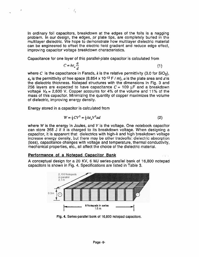
Performance of a NoteDad CaDacitor Bank
A conceptual design for a 20 KV, 6 MJ series-parallel bank of 16,800 notepadcapacitors is shown in Fig. 4. Specifications are listed in Table 3.
8NOWP* in wi6s
t----- ““ ---1
Fig. 4. Series-parallelbankof 16,600 notepadcapacitors.
Page-9.

Volume:
Capacitance:
Working voltage:
Energy storage:
Weight:
Energy density:
Specific energy:
Effective Series Resistance:
—
1.0 m3
0.03 F
20 Kv
6 MJ
3000 Kg
6 MJ/m3
2 KJ/Kg
0.3 mL?
Table3.Capacitorbankspecifications.
To examine the efficiency of this capacitor bank, a simplified model of anelectromagnetic propulsion (railgun) application was devised, represented byan RL load with R=O.2 Q and L=2 mH. This initial charge was 20 KV, 6 MJ. Withthese conditions, the expected voltage ringdown occurred with voltage reversalat 17 ms. Losses in the capacitor bank include 3 KJ of Izl? loss in the conductorsand 6 KJ of dielectric loss, for a bank efficiency of 99.85’% (refer to Table 4). In apractical system, much more energy would be lost externally in a resistivecrowbar circuit that is required to prevent voltage reversal and quench anyarcing on the railgun.
Resistive loss: 3 KJ
Dielectric loss: 6 KJ
Bank efficiency: 99.85 %
Heating per shot: o.007°C
Table 4. Expected capacitor bank performance, pulse application.
Little heating of the bank (a 0.007°C rise per shot) would occur because of itshigh efficiency and high heat capacity. The heat capacities of the capacitormaterials relative to water (water = 1.0) are 0,54 for Si02 and 0.89 for copper.Use of thin layers also promotes rapid thermal diffusion, preventing internalstress. This looks very favorable for high repetition rate applications. It isfeasible to build in liquid cooling channels if different geometries or materialsthat require cooling were used.
Page -10-

Desian Su mmary
This conceptual design uses well-understood materials to engineer a design foran extraordinary capacitor. High energy density, low loss, good thermal andmechanical properties, and low inductance make the nano-structure multilayercapacitor an excellent candidate for military pulse power applications.
TECHNICAL STATUS AND ISSUES
Our nano-structure multilayer technology is well established. Facilities andequipment capable of proof-of-principal and small scale capacitor fabricationand testing is available. We are capable and prepared to retrofit and add to theexisting systems to carry out Phase 1 of the proposed program. Our scientificand engineering staff is currently in place and available for this program. Weare prepared to draw on the collective materials, pulse power and relatedexpertise at LLNL needed to succeed in this program.
Some important technology issues need to be investigated. Time dependentdielectric breakdown of nano-structure multilayer capacitors need to be wellunderstood for a variety of materials and capacitor designs. Intetfacial reactions(e.g., diffusion) between dielectrics and conductors are important to understandvoltage breakdown phenomena. Complex dielectric-conductor structures andmultiple dielectric-dielectic interfaces that are expected to provide very highvoltage holdoff will be studied. Amorphous, complex-composition dielectricsmay offer advantages. Voltage breakdown resulting from electromagnetic fieldgradients at the edges of conductors is a concern.
Program issues include development and fabrication of the first nano-structuremultilayer capacitors designed for high voltage holdoff. Substrates andsubstrate removal to fabricate free standing capacitors have to be developed.Full capacitor time and temperature holdoff and discharge performancecharacterization need to be done. We need a better understanding ofengineering design of near-net-form capacitors with consideration toelectromagnetic gradients and edge effects, mechanical properties andinterconnection for integration in capacitor banks. Scale up of this nano-structure capacitor te~hnology wili requireequipment, and will present new fabrication and
PLANNED WORK
investment in facilities andprocessing problems.
Our efforts will be divided into two phases. Phase 1 encompasses proof ofprinciple capacitor fabrication, materials research, device engineering, and thedesign of a scaled-up capacitor fabrication facility. If Phase 1 is successful,
Page -11-

,,-..
Phase 2 will follow with the construction of the facility, design and testing ofnotepad capacitors for a capacitor bank demonstration, and the design of high-volume manufacturing equipment for industry.
Phase 1 [Durwon. 15 me@@. .
1. Proof-of-principle capacitor: An existing LLNL research facility will beupgraded to support fabrication of small scale multilayer capacitors. Deviceswill be fabricated from several materials, followed by electrical characterizationand mechanical testing to establish the viability of this technology. Deliverables:Progress and test reports.
2. Materials Studies & Modeling: Throughout Phase 1, we will be improvingour physical models and understanding of nano-structure multilayer dielectrics,accumulating a database of dielectric characteristics, and performing electricalsystem analyses. These models will effect capacitor design and improveperformance. Deliverables: Database and modeling repott.
3. Second-generation capacitor: Buildingon our knowledge gained in theprevious steps, the facility will be modified as required, new capacitor designsand materials will be fabricated and extensive testing will be performed.Deliverables: Progress and test reports; characterized small scale capacitor(s)for independent evaluation.
4. Fabrication facility design: As this technology shows progress, we wiildesign a scaled-up capacitor fabrication facility that will be used to make theproposed notepad capacitors. Deliverables: Facility design documents.
Successful completion of Phase 1 with encouraging findings would lead toapproval and funding to proceed with Phase 2.
phase 2 {Du ration: 21 months}
7. Materials Studies & Modeling: Continuation of Phase 1 materials researchand engineering modeling efforts. Deliverables: Database and modelingreport.
2. Fabrication Faci/ity Construction: Procurement, construction and checkoutof the Notepad capacitor fabrication capability at LLNL. Deliverables:Completed facility.
3. Notepad Capacitors: Design, fabricate, characterize and test of individualnotepad capacitors using various materials and geometries. These will be full-scale devices, usable in pulse power applications. Deliverables: Progressreport; characterized Notepad capacitor(s).
Page-12-

‘.
4. Capacitor Bank: Design, fabricate, and test a demonstration pulse powercapacitor bank made up of tens of notepad capacitors, includinginterconnection, charging and switching systems. The bank will be tested withloads that are representative of the desired application. Deliverables: Finalreport.
5. Manufacturing: Work with designated DoD contractors to design acommercial manufacturing facility capable of high-volume capacitor production.Deliverables: Conceptual plant d~sign.
PROJECT FUNDING
Phase 1 Q1 , FY93 -through- QI , FY94
Ph=e Z Q2, FY94 -through- Q4, FY95
$1,500 K
$3,000 K
RELATED ON-GOING WORK
LLNL is an applied physics laboratory with a well established materials andengineering technology base. We expect to draw on the collective capabilitiesand expertise at LLNL to better understand the pulse power application and bein the best position to meet DNA’s capacitor performance goals. Core materialstechnologies include the nano-structure multilayers, interatomic materialsdiagnostics, and carbon and silica aerogels. Multilayers are currently beingdeveloped as physics diagnostic and optical devices. Research is proceedingto take advantage of their remarkable mechanical and thermal properties forDOE Weapons programs and applications in aerospace and related industries.The transmission electron microscopes x-ray diffraction and similar diagnosticcapabilities at LLNL are needed tools to understand and develop nano-structure multilayer materials. Carbon aerogels are extremely low density, highsurface area foams developed for DOE programs. We are currently developinglow voltage, very high capacitance electrolytic capacitors with carbon aerogelsto replace batteries in some applications.
LLNL also has well developed engineering thrust areas in pulse power,microwave, laser and semiconductor technologies, and electromagnetic anddevice modeling. Very large capacitor banks have been developed for electricgun, rail gun and x-ray applications. LLNL originated small pulse power slapperdetonators for weapon initiation. Microwave broad band sources andvulnerability assessment at LLNL rely on high performance capacitortechnology. Pulsed, high power lasers developed at LLNL for DOE and DoDprograms similarly rely on high performance capacitors banks. Research hasbeen done on laser and electron beam initiated fast semiconductor switches forpulse power applications. Our electromagnetic and device modeling expertiseis a resource used by DOE and DoD programs.
Page -13-

EXPECTED PAYOFFS
We are proposing research and development of an important enablingtechnology. The nano-structure multilayer capacitor technology can open upmany new opportunities for the military and industry. An order of magnitude ormore improvement in energy density with very high efficiency can be significant.We can expect immediate use of this capacitor technology in electro-thermaland electromagnetic effects programs, and possibly rail-gun, laser and x-raygeneration programs. Their applications in weapons initiation and smartpenetrator fuzing is anticipated, and use in space and other remote applicationswill surely arise.
The proposed technology may enable capacitor designs that approachtheoretical limits of the dielectric and conductor materials used. New capacitordesign techniques are made possible to control field gradients, edge effectsand current densities in the capacitor, and enable rugged, high densitycapacitor bank packaging for militaty and space applications.
We plan to move this technology to DNA industrial partners in Phase 2 of theprogram. We will be available to support military application commercializationthis new technology with DNA and pulse power community.
The revitalization of the American electronics and industrial base is alsoimportant. The proposed capacitor technology can make a needed difference ina variety of industrial fields. Communication and transportation systemsenvisioned today can be enabled and made practical by high energy densitycapacitor technology. Electric automobiles with reasonable acceleration andeffective energy recovety through dynamic breaking may become a reality withthis technology. Medical systems, such as defibrillator implants, and highdensity electronics packaging can be made possible.
Page -14-

‘w. .
MULTILAYER CAPACITOR DEVELOPMENT SCHEDULE REV: 8-19-92
MONTHS FROM STARTTask O 3 6 9 12 15 18 21 24 27 30 33 36
$@ Proof-of-Principle Capacitor
Facility preparation
:’ Nlsterlals Studies& Modeling
;#: Database dielectrics characteristics
Electrical network analysis
neration Capacitor
Facilky preparation
II,.,...........&&,@brication Facility
~~~ Faality design,,.:.,~.::= A~rove phase2
~ ~eting 11
~ Database dielectrics characteristics
~ Fabrication Facility
! procurements
construction
‘ checkout
~ ~tepad Capacitor
~ Design
~ Fabrication
~ Testing
Report
@pacttor Bank
Desgn:?::,~,;:::::i::~:::;:,:;:;: Fabrication:.:.:...,,.....
Testing
Report
I I II 14[1
I I I1 1 1
I 1 I
I I I1I RI I,-1I 1 pI I1 1 I
I I 1I I II I I
_LL-l--1 i II I 1I I I
I I II I II 1 1I I I1’1”1I I I
I I II I II I II I II I II 1 1I I I1 I II I 1
I I II I II I II I II I II I II 1 ,
I I 1I I JI 1 II I II I I
1 I I
I I 1I I II I II I 1I I II I II I II I I1 I II I I
-A I II I
I I Ii I I
—1 I 1
-A I II
~i 1 I
4 I II 1
-LL--L-1 I 1
-
I I II 1 1
-
I I II 1 11 1 1I 1 11 1 1I 1 I
I I 11 I I1 1 II I II I II I II I II I II I 11 I 1I I II I I
I I I
I I II 1 II I II I II I II I II I II-14-AI I II I 1I 1 I
_L-L-L-1 I 1I I II I I1 I 1I t II I II I II I II I II I II I II I I
-L-L-L-1 1 I
-
I I I1 I II I II I 1I I I
I I I
I I I
-
u;I I-4I I I
I I II-1
I 1-1 II I 1=
1 I II II -
Page -15-

Technical Inform
ation Departm
ent • Lawrence Liverm
ore National Laboratory
University of C
alifornia • Livermore, C
alifornia 94551


