DESCRIPTION The ZXCD1000 provides complete control and modulation functions at the heart of a high efficiency high performance Class D switching audio amplifier solution. In combination with Zetex HDMOS MOSFET devices, the ZXCD1000 provides a high performance audio amplifier with all the inherent benefits of Class D. The ZXCD1000 solution uses proprietary circuit design to realise the true benefits of Class D without the traditional drawback of poor distortion performance. The combination of circuit design, magnetic component choice and layout are essential to realising these benefits. FEATURES • >90% efficiency • 4 / 8 Ω drive capability • Noise Floor -115dB for solution • Flat response 20Hz - 20kHz • High gate drive capability ( 2200pF) • Very low THD + N 0.2% typical full 90% power, full band ( for the solution) • Complete absence of crossover artifacts • OSC output available for sync in multi-channel applications • Available in a 16 pin exposed pad QSOP package APPLICATIONS • DVD Players • Automotive audio systems • Home Theatre • Multimedia • Wireless speakers • Portable audio • Sub woofer systems • Public Address system The ZXCD1000 reference designs give output powers up to 100W rms with typical open loop (no feedback) distortion of less than 0.2% THD + N over the entire audio frequency range at 90% full output power. This gives an extremely linear system. The addition of a minimum amount of feedback (10dB) further reduces distortion figures to give < 0.1 % THD + N typical at 1kHz. From an acoustic point of view, even more important than the figures above, is that the residual distortion is almost totally free of any crossover artifacts. This allows the ZXCD1000 to be used in true hi-fi applications. This lack of crossover distortion, sets the ZXCD1000 solutions quite apart from most other presently available low cost solutions, which in general suffer from severe crossover distortion problems. ZXCD1000 ISSUE 2 - APRIL 2002 1 HIGH FIDELITY CLASS D AUDIO AMPLIFIER SOLUTION Output Power 1W 5W 10W THD + N (%) Distortion v Power 8Ω open loop at 1kHz. The plot shows Distortion v Power into an 8Ω load at 1kHz. This plot clearly demonstrates the unequalled performance of the Zetex solution. Typical distortion of 0.05% at 1W can be seen with better than 0.15% at 10W. Truly world class performance.
Transcript
DESCRIPTION
The ZXCD1000 provides complete control andmodulation functions at the heart of a high efficiencyhigh performance Class D switching audio amplifiersolution. In combination with Zetex HDMOS MOSFETdevices, the ZXCD1000 provides a high performanceaudio amplifier with all the inherent benefits of Class D.
The ZXCD1000 solution uses proprietary circuit designto realise the true benefits of Class D without thetraditional drawback of poor distortion performance.The combination of circuit design, magneticcomponent choice and layout are essential to realisingthese benefits.
FEATURES
• >90% efficiency
• 4 / 8 Ω drive capability
• Noise Floor -115dB for solution
• Flat response 20Hz - 20kHz
• High gate drive capability ( 2200pF)
• Very low THD + N 0.2% typical full 90% power, fullband ( for the solution)
• Complete absence of crossover artifacts
• OSC output available for sync in multi-channelapplications
• Available in a 16 pin exposed pad QSOP package
APPLICATIONS
• DVD Players
• Automotive audio systems
• Home Theatre
• Multimedia
• Wireless speakers
• Portable audio
• Sub woofer systems
• Public Address system
The ZXCD1000 reference designs give output powersup to 100W rms with typical open loop (no feedback)distortion of less than 0.2% THD + N over the entireaudio frequency range at 90% full output power. Thisgives an extremely linear system. The addition of aminimum amount of feedback (10dB) further reducesdistortion figures to give < 0.1 % THD + N typical at1kHz.
From an acoustic point of view, even more importantthan the figures above, is that the residual distortion isalmost totally free of any crossover artifacts. Thisallows the ZXCD1000 to be used in true hi-fiapplications. This lack of crossover distortion, sets theZXCD1000 solutions quite apart from most otherpresently available low cost solutions, which in generalsuffer from severe crossover distortion problems.
ZXCD1000
ISSUE 2 - APRIL 2002
1
HIGH FIDELITY CLASS D AUDIO AMPLIFIER SOLUTION
Output Power
1W5W
10W
TH
D +
N (
%)
Distortion v Power
8Ω open loop at 1kHz.
The plot shows Distortion v Power into an 8Ω load at1kHz. This plot clearly demonstrates the unequalledperformance of the Zetex solution. Typical distortion of0.05% at 1W can be seen with better than 0.15% at 10W.Truly world class performance.
ISSUE 2 - APRIL 2002
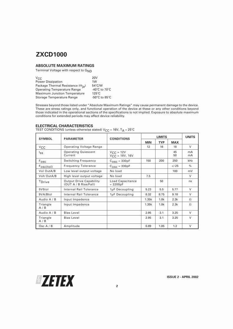
ABSOLUTE MAXIMUM RATINGS
Terminal Voltage with respect to GND
VCC 20VPower Dissipation 1WPackage Thermal Resistance (ja) 54C/WOperating Temperature Range -40C to 70CMaximum Junction Temperature 125CStorage Temperature Range -50°C to 85C
Stresses beyond those listed under “Absolute Maximum Ratings” may cause permanent damage to the device.These are stress ratings only, and functional operation of the device at these or any other conditions beyondthose indicated in the operational sections of the specifications is not implied. Exposure to absolute maximumconditions for extended periods may affect device reliability.
ZXCD1000
2
SYMBOL PARAMETER CONDITIONSLIMITS UNITS
MIN TYP MAX
VCC Operating Voltage Range 12 16 18 V
Iss Operating QuiescentCurrent
VCC = 12VVCC = 18V, 16V
4550
mAmA
Fosc Switching Frequency Cosc = 330pF 150 200 250 kHz
Fosc(tol) Frequency Tolerance Cosc = 330pF +/-25 %
Vol OutA/B Low level output voltage No load 100 mV
Voh OutA/B High level output voltage No load 7.5 V
TDrive Output Drive Capability(OUT A / B Rise/Fall)
Load Capacitance= 2200pF
50 ns
5V5tol Internal Rail Tolerance 1µF Decoupling 5.23 5.5 5.77 V
9VA/Btol Internal Rail Tolerance 1µF Decoupling 8.32 8.75 9.18 V
5 Cosc External timing capacitor node (to set the switching frequency)
6 Osc B Triangle Output (for slave ZXCD1000 in stereo application)
7 Triangle B Triangle Input for Channel B
8 Audio B Audio Input for Channel B
9 Gnd Small Signal GND
10 OUT B Channel B PWM Output to drive external Bridge MOSFETs
11 Gnd2 Power GND (for Output Drivers)
12 9VB Internal Supply Rail (Decouple with 1µF Cap)
13 VCC Input Supply Pin (Max = 18V)
14 9VA Internal Supply Rail (Decouple with 1µF Cap).
15 OUT A Channel A PWM Output to drive external Bridge MOSFETs
16 5V5 Internal Supply Rail (Decouple with 1µF Cap)
Pin Description
ISSUE 2 - APRIL 2002
ZXCD1000 Class D controller IC
A functional block diagram of the ZXCD1000 is shownin Figure 2. The on chip series regulators drop theexternal VCC supply (12V-18V) to the approximate 9V(9VA/9VB) and 5.5V (5V5) supplies required by theinternal circuitry.
A triangular waveform is generated on chip and isbrought out at the OscA and OscB outputs. Thefrequency of this is set (to ~200kHz) by an externalcapacitor (Cosc) and on chip resistor. The triangularwaveform must be externally AC coupled back into theZXCD1000 at the TriangleA and TriangleB inputs.
AC coupling ensures symmetrical operation resultingin minimal system DC offsets. TriangleA is connectedto one of the inputs of a comparator and TriangleB isconnected to one of the inputs of a second comparator.The other inputs of these two comparators areconnected to the AudioA and AudioB inputs, which areanti-phase signals externally derived from the audioinput. The triangular wave is an order higher infrequency than the audio input (max 20kHz). Theoutputs of the comparators toggle every time theTriangleA/B and the (relatively slow) AudioA/B signalscross.
ZXCD1000
4
Oscillator & RampGenerator
Internal 5V5
Internal 9V
PWMComp A
PWMComp B
Pre-Driver
Pre-Driver
O/PDriver
O/PDriver
Audio A
Audio B
VCC
Cos
c
Out A
Out B
5V5
9VB
9VA
Tria
ngle
B
Tria
ngle
A
Osc
B
Osc
A
Dis
t
Gnd
Gnd
2
1
234 5 6 7
8
9
10
1112
13
14
15
16
OscBuffers
Figure 2.Functional Block Diagram
With no audio input signal applied, the AudioA/Binputs are biased at the mid-point of the triangularwave, and the duty cycle at the output of thecomparators is nominally 50%. As the AudioA/B signalascends towards the peak level, the crossing pointswith the (higher frequency) triangular wave alsoascend. The comparator monitoring these signalsexhibits a corresponding increase in output duty cycle.Similarly, as the AudioA/B signal descends, the dutycycle is correspondingly reduced. Thus the audio inputPulse Width Modulates the comparator outputs. Thisprinciple is illustrated in Figures 3a, b, c and d. Thecomparator outputs are buffered and used to drive theOutA and OutB outputs. These in turn drive the speakerload (with the audio information contained in the PWMsignal) via the off chip output bridge and single stageL-C filter network.
The ramp amplitude is approximately 1V. The AudioA,AudioB, TriangleA and TriangleB inputs are internallybiased to a DC voltage of approximately VCC/5. Themid - point DC level of the OscA and OscB triangularoutputs is around 2V. The triangular wave at the Coscpin traverses between about 2.7Vand 3.8V and the distpin exhibits a roughly square wave from about 1.4V to2V. (The above voltages may vary in practice and areincluded for guidance only).
ZXCD1000
ISSUE 2 - APRIL 2002
5
Audio A/B
Triangle A/B
PWM Comparator
O/P
Audio A/B
Triangle A/B
Comparator O/P(Duty Cycle = 50%)
O/P
Audio A/B
Triangle A/B
Comparator O/P(Duty Cycle = 75%)
Audio A/B
Triangle A/B
Comparator O/P(Duty Cycle = 25%)
Figure 3b.Figure 3a.
Figures 3a,3b,3c and 3dThe audio input Pulse Width Modulates the comparator output.
Figure 3c. Figure 3d.
ISSUE 2 - APRIL 2002
ZXCD1000
6
Fig
ure
4
Zete
xC
lass
D25W
Mo
no
Op
en
Lo
op
So
luti
on
Class D 25W Mono Open Loop (Bridge Tied Load - BTL) Solution – Circuit Description
Proprietary circuit design and high quality magneticsare necessary to yield the high THD performancespecified. Deviation from the Zetex recommendedsolution could significantly degrade performance.
The speaker is connected as a Bridge Tied Load (BTL).This means that both sides of the speaker are drivenfrom the output bridge and therefore neither side of thespeaker connects to ground. This allows maximumpower to be delivered to the load, from a given supplyvoltage. The supply voltage for this solution isnominally 16V for 25W into a 4 load.
A schematic diagram for the solution is shown inFigure 4. The audio input is AC coupled and applied to alow pass filter and a phase splitter built around theNE5532 dual op-amp. One of these op-amps isconfigured as a voltage follower and the other as a X1inverting amplifier. This produces in phase andinverted signals for application to the ZXCD1000. Theop-amp outputs are AC coupled into the ZXCD1000Audio A and Audio B inputs via simple R-C low passfilters (R16/C3 and R15/C7). The op-amps are biased toa DC level of approximately 6V by R11 and R12.
The Pulse Width Modulated (PWM) outputs, OutA andOutB, which contain the audio information, are ACcoupled and DC restored before driving the ZetexZXM64P03X and ZXM64N03X PMOS and NMOSoutput bridge FET’s. AC coupling is via C17, C18, C19and C20. DC restoration is provided by the D2(A1a)/R4,D1(A4a)/R2 and D3(A1a)/R6, D4(A4a)/R9 components.This technique allows the output stage supply voltageto be higher than the high level of the OutA and OutBoutputs (approximately 8.5V), whilst still supplyingalmost the full output voltage swing to the gates of thebridge FET’s (thereby ensuring good turn on). This canbe exploited to yield higher power solutions withhigher supply voltages – this is discussed later.
The resistor/diode combinations (R5/D2(A16b),R3/D1(A4b), R7/D3(A1b) and R8/D4(A4b)) in series withthe bridge FET gates, assist in controlling the switchingof the bridge FET’s. This design minimises shootthrough currents whilst still achieving the lowdistortion characteristics of the system.
The purpose of the special inductors in conjunctionwith the output capacitors C23, C24, C25 and C26 is tolow pass filter the high frequency switching PWMsignal that comes from the bridge. Thus the lowerfrequency audio signal is recovered and is available atthe speakerA and speakerB outputs across which thespeaker should be connected. Zetex can offer advice onsuitable source for the specialist magnetics.
The optional components R17 and C3 form a Zobelnetwork. The applicability of these depends upon theapplication and speaker characteristics. Suggestedvalues are 47nF and 10 ohms
Efficiency
The following plots show the measured efficiency ofthe Zetex solution at various power levels into both 4Ωand 8Ω loads. As a comparison, typical efficiency isplotted for a class A-B amplifier. They clearlydemonstrate the major efficiency benefits availablefrom the Zetex class D solution.
ZXCD1000
ISSUE 2 - APRIL 2002
7
Figure 5
ISSUE 2 - APRIL 2002
ZXCD1000
8
Class D Mono Open Loop solution (Bridge Tied Load - BTL) Solution - Demonstration board
The circuit design shown in figure 4 is available as ademonstration board to enable evaluation of the circuitexcellent performance. Full bill of materials (BOM) andGerber files are also available. The demonstrationboard part number is ZXCD1000EVMOL. Layout andcomponent selection are critical to maximisingperformance from this solution, the demonstrationboard and circuit can be used as a guide to facilitatedesign of production circuits. Zetex applications canadvise if any circuit modifications are required forspecific requirements.
The board can be used to demonstrate the ZXCDamplifier capability with output power typically of 25Winto 4 or 8 load depending on chosen supplyvoltage. Operating instructions are included in thedemonstration board literature.
A very important feature of the Zetex solution is thatthe residual distortion is almost totally free of anycrossover artifacts. This lack of crossover distortionsets the ZXCD1000 solutions quite apart from mostother presently available low cost solutions, which ingeneral suffer from severe crossover distortionproblems.
It is well known that this kind of distortion is particularlyunpleasant to the listener. The two scope traces ofFigure 7 clearly show the lack of such artifacts with theZetex solution
Figure 7aZETEX Class D Solution. (10W into 4Ω)Note lack of Crossover Artifacts
Figure 7bTypical Class D Solution.Note Large Crossover Artifacts
Figure 6Mono solution demonstration board
Other Solutions - Stereo, Closed Loop and Higher Powers.
STEREO
It is possible to duplicate the above solution to give a 2channel stereo solution. However if the oscillatorfrequencies are not locked together, a beat can occurwhich is acoustically audible. This is undesirable. Astereo solution which avoids this problem can beachieved by synchronising the operating frequenciesof both ZXCD1000’s class D controller IC’s, by slavingone device from the other. This is illustrated in Figure 8.
Great care must be taken when linking the trianglefrom the master to the slave. Any pickup can causeslicing errors and result in increased distortion. Thebest connection method is to run two tracks, side byside, from the master to the slave. One of these trackswould be the triangle itself, and the other would be thedirect local ground linking the master pin9 ground tothe slave pin 9 ground.
A demonstration board, ZXCD1000EVSOL, is availablefor a stereo 25W solution.
ZXCD1000
ISSUE 2 - APRIL 2002
9
MASTER SLAVE
Figure 8 Frequency synchronisation for stereo applications
ISSUE 2 - APRIL 2002
ZXCD1000
10
Fig
ure
9
50W
Maste
rC
han
nelw
ith
feed
back
Class D 50W Mono Bridge Tied Load (BTL)Solution with Feedback – Circuit Description
With the addition of feedback (hence closed loopsolution) it is possible to obtain even better THDperformance. A schematic diagram for this is shown inFigure 9. Again proprietary circuit and specialmagnetic design is necessary to yield the high THDperformance and deviation from this couldsignificantly reduce performance.
Much of the circuitry is the same as described for theopen loop solution. The main differences being aconsequence of using the feedback circuitry. The audioinput is ac coupled and applied to an op-amp (1/2 of U3)configured as a non–inverting amplifier with a gain ofapproximately 4. Feedback is applied differentiallyfrom the bridge outputs via the other half of U3op-amp. A portion of the single ended output from thisop-amp is subtracted from the output of thenon-inverting op-amp output above. Overall negativefeedback is applied due to the polarity and connectionof the signals involved.
The audio signal from the above circuitry is applied to aphase splitter as was done for the open loop solution.This is built around the other 5532 dual op-amp (U2).One of these op-amps is configured as a voltagefollower and the other as a X1 inverting amplifier. Thisproduces in phase and inverted signals for applicationto the ZXCD1000 Audio A and Audio B inputsrespectively.
The output circuitry downstream of the ZXCD1000 is asdescribed for the open loop solution. In order tosupport the 50W output power of this solution a 25Vrail is required for a 4 load. The MOSFETs used areSOT223 packaged (ZXM64N035G and ZXM64P035).
Further information on this design is available throughZetex applications.
Higher Power Solutions
With some modifications the applications solutionscan be extended to give output power up to 100W. Themain differences being the supply voltage, the TO220MOSFETs, and the output magnetics. The magneticsfor 100W are necessarily larger than required for25/50W in order to handle the higher load currents. For100W operation the supply voltage to the circuit isnominally 35V with a 4 load. However the maximumsupply voltage to the ZXCD1000 class D controller IC is18V, hence a voltage dropper is required. This could bedone, for example, as in the open loop solutiondescribed previously. A 100W circuit is shown onfigure 10. This features a 35V bridge supply TO220MOSFETs (ZXM64N035L3 and ZXM64P035L3) andalso proposed protection circuits for over current andover temperature and an alternative anti pop circuit.Further information on this 100W reference design canbe obtained through Zetex applications.
The ZXCD1000 class D controller IC is inherentlycapable of driving even higher power solutions, withthe appropriate external circuitry. However as statedabove the maximum supply voltage to the ZXCD1000class D controller IC is 18V and the higher supplyvoltages must therefore be dropped. Also dueconsideration must be given to the ZXCD1000 outputdrive levels and the characteristics of the bridgeMOSFET’s. The latter must be sufficiently enhanced bythe OutA and OutB outputs to ensure the filter and loadnetwork is driven properly. If the gate drive of theZXCD1000 is too low for the chosen MOSFET then theOUTA and OUTB signal must be buffered using anappropriate MOSFET driver circuit. Additionally,suitable magnetics are essential to achieve good THDperformance.
Package details
The ZXCD1000 is available in a 16 pin exposed padQSOP package. The exposed pad on the underside ofthe package should be soldered down to an area ofcopper on the PCB, to function as a heatsink. The PCBshould have plated through vias to the underside of theboard, again connecting to an area of copper.
ZXCD1000
ISSUE 2 - APRIL 2002
11
ISSUE 2 - APRIL 2002
ZXCD1000
12
Fig
ure
10
100W
Mo
no
Cla
ss
DS
olu
tio
n
ZXCD1000 Solution performance figures
Typical performance graphs for the Zetex 25W openloop solution are shown here for both 4 and 8Ω loads.These graphs further demonstrate the true high fidelityperformance achieved by the Zetex solutions.
ZXCD1000
ISSUE 2 - APRIL 2002
13
Output Power
1W5W
10W
TH
D +
N (
%)
f(Hz)
dB
f(Hz)
dB
f(Hz)
dB
THD v Power into 8 at 1kHz FFT of distortion and noise floor at 1W (8 load)
FFT of distortion and noise floor at 10W (8 load)Frequency response (8 load)
ISSUE 2 - APRIL 2002
ZXCD1000
14
Output Power
1W 5W10W
20W
TH
D +
N (
%)
dB
f(Hz)
f(Hz)
dB
f(Hz)
dB
FFT of distortion and noise floor at 20W (4 load)Frequency response (4 load)
Note roll off.This can be corrected by using an alternative values foroutput filter components.
THD v Power into 4 at 1kHz FFT of distortion and noise floor at 1W (4 load)
These offices are supported by agents and distributors in major countries world-wide.
This publication is issued to provide outline information only which (unless agreed by the Company in writing) may not be used, applied or reproducedfor any purpose or form part of any order or contract or be regarded as a representation relating to the products or services concerned. The Companyreserves the right to alter without notice the specification, design, price or conditions of supply of any product or service.
For the latest product information, log on to www.zetex.com
Information on Zetex reference designs, MOSFETs and demonstration boards can be obtain by contacting Zetexapplications or by visiting www.zetex.com/audio