+ All Categories
Home > Documents > High mobility organic thin film transistor and efficient photovoltaic devices using versatile...

High mobility organic thin film transistor and efficient photovoltaic devices using versatile...

Date post: 18-Dec-2016
Category:
Upload: ananth
View: 212 times
Download: 0 times
Share this document with a friend
9
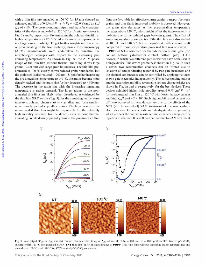
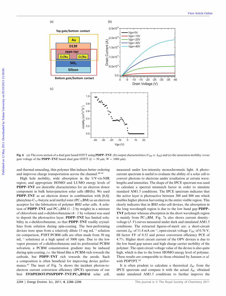
High mobility organic thin film transistor and efficient photovoltaic devices using versatile donor–acceptor polymer semiconductor by molecular design Prashant Sonar, * a Samarendra P. Singh, a Yuning Li, * ab Zi-En Ooi, a Tae-jun Ha, c Ivy Wong, a Mui Siang Soh a and Ananth Dodabalapur * ac Received 23rd February 2011, Accepted 11th April 2011 DOI: 10.1039/c1ee01213d In this work, we report a novel donor–acceptor based solution processable low band gap polymer semiconductor, PDPP–TNT, synthesized via Suzuki coupling using condensed diketopyrrolopyrrole (DPP) as an acceptor moiety with a fused naphthalene donor building block in the polymer backbone. This polymer exhibits p-channel charge transport characteristics when used as the active semiconductor in organic thin-film transistor (OTFT) devices. The hole mobilities of 0.65 cm 2 V 1 s 1 and 0.98 cm 2 V 1 s 1 are achieved respectively in bottom gate and dual gate OTFT devices with on/off ratios in the range of 10 5 to 10 7 . Additionally, due to its appropriate HOMO (5.29 eV) energy level and optimum optical band gap (1.50 eV), PDPP–TNT is a promising candidate for organic photovoltaic (OPV) applications. When this polymer semiconductor is used as a donor and PC 71 BM as an acceptor in OPV devices, high power conversion efficiencies (PCE) of 4.7% are obtained. Such high mobility values in OTFTs and high PCE in OPV make PDPP–TNT a very promising polymer semiconductor for a wide range of applications in organic electronics. Introduction Semiconducting polymers are important functional materials for low cost printed electronic devices, particularly for use as active materials in organic thin-film transistors (OTFTs), organic photovoltaics (OPVs), chemical sensors, etc. 1–5 High perfor- mance semiconducting polymers are being widely pursued aim- ing for improved device performance to overcome the limitations of existing organic electronics. The optoelectronic properties of polymer semiconductors are primarily governed by the conju- gated blocks incorporated in the polymeric backbone. It has been well proven that the utilization of electron donating (D) and accepting (A) building blocks in the main backbone is one of the most promising and attractive strategies for making low band gap organic semiconducting polymers i. 6–8 Selection of such D–A building blocks in a conjugated backbone requires special attention paid to certain properties such as electron donating or accepting capability, planarity, chemical-electrochemical stability, and efficient tunability in electronic characteristics through side chain substitution and solid state self-assemblies. Such a D–A combination allows for band gap tuning through hybridization of the highest occupied molecular orbital (HOMO) of the donor moiety with the lowest unoccupied molecular orbital (LUMO) of the acceptor moiety. Semiconducting poly- mers with low band gaps with wide absorption covering from UV-vis to NIR regions are expected to be potential light har- vesting materials for OPV devices. 9 A D–A system also induces intermolecular D–A interactions, leading to increased molecular ordering through self-assembly of the polymer main chains. As a result, exceptionally high mobility has been observed for certain D–A polymers in OTFT devices. 10–13 The planar pyrrolo- [3,4-c]pyrrole-1,4(2H,5H)-dione or diketopyrrolopyrrole (DPP) a Institute of Materials Research and Engineering (IMRE), Agency for Science, Technology, and Research (A*STAR), 3 Research Link, Singapore 117602. E-mail: [email protected]; yuning.li@ uwaterloo.ca; [email protected] b Department of Chemical Engineering, University of Waterloo, 200 University Avenue West, Waterloo, Ontario, Canada N2L 3G1 c Microelectronics Research Center, The University of Texas at Austin, Austin, TX, 78758, USA Broader context Donor–acceptor based solution processable polymers are an emerging class of materials for organic electronic device applications. Incorporation of fused aromatic donor and acceptor building blocks in the polymer backbone induces a strong tendency to form pp stacks with a large overlapping area. Such materials are preferable for effective charge carrier transport through intermolecular hopping in OFET devices and also have optimum band gaps for OPV devices. 2288 | Energy Environ. Sci., 2011, 4, 2288–2296 This journal is ª The Royal Society of Chemistry 2011 Dynamic Article Links C < Energy & Environmental Science Cite this: Energy Environ. Sci., 2011, 4, 2288 www.rsc.org/ees PAPER Published on 12 May 2011. Downloaded by Tulane University on 05/10/2013 15:59:00. View Article Online / Journal Homepage / Table of Contents for this issue
Transcript

Dynamic Article LinksC<Energy &Environmental Science

Cite this: Energy Environ. Sci., 2011, 4, 2288

www.rsc.org/ees PAPER

Publ

ishe

d on

12

May

201

1. D

ownl

oade

d by

Tul

ane

Uni

vers

ity o

n 05

/10/

2013

15:

59:0

0.

View Article Online / Journal Homepage / Table of Contents for this issue

High mobility organic thin film transistor and efficient photovoltaic devicesusing versatile donor–acceptor polymer semiconductor by molecular design

Prashant Sonar,*a Samarendra P. Singh,a Yuning Li,*ab Zi-En Ooi,a Tae-jun Ha,c Ivy Wong,a Mui Siang Soha

and Ananth Dodabalapur*ac

Received 23rd February 2011, Accepted 11th April 2011

DOI: 10.1039/c1ee01213d

In this work, we report a novel donor–acceptor based solution processable low band gap polymer

semiconductor, PDPP–TNT, synthesized via Suzuki coupling using condensed diketopyrrolopyrrole

(DPP) as an acceptor moiety with a fused naphthalene donor building block in the polymer backbone.

This polymer exhibits p-channel charge transport characteristics when used as the active semiconductor

in organic thin-film transistor (OTFT) devices. The hole mobilities of 0.65 cm2 V�1 s�1 and 0.98 cm2 V�1

s�1 are achieved respectively in bottom gate and dual gate OTFT devices with on/off ratios in the range

of 105 to 107. Additionally, due to its appropriate HOMO (5.29 eV) energy level and optimum optical

band gap (1.50 eV), PDPP–TNT is a promising candidate for organic photovoltaic (OPV) applications.

When this polymer semiconductor is used as a donor and PC71BM as an acceptor in OPV devices, high

power conversion efficiencies (PCE) of 4.7% are obtained. Such high mobility values in OTFTs and

high PCE in OPV make PDPP–TNT a very promising polymer semiconductor for a wide range of

applications in organic electronics.

Introduction

Semiconducting polymers are important functional materials for

low cost printed electronic devices, particularly for use as active

materials in organic thin-film transistors (OTFTs), organic

photovoltaics (OPVs), chemical sensors, etc.1–5 High perfor-

mance semiconducting polymers are being widely pursued aim-

ing for improved device performance to overcome the limitations

of existing organic electronics. The optoelectronic properties of

polymer semiconductors are primarily governed by the conju-

gated blocks incorporated in the polymeric backbone. It has been

well proven that the utilization of electron donating (D) and

aInstitute of Materials Research and Engineering (IMRE), Agency forScience, Technology, and Research (A*STAR), 3 Research Link,Singapore 117602. E-mail: [email protected]; [email protected]; [email protected] of Chemical Engineering, University of Waterloo, 200University Avenue West, Waterloo, Ontario, Canada N2L 3G1cMicroelectronics Research Center, The University of Texas at Austin,Austin, TX, 78758, USA

Broader context

Donor–acceptor based solution processable polymers are an emerg

Incorporation of fused aromatic donor and acceptor building block

p stacks with a large overlapping area. Such materials are preferab

hopping in OFET devices and also have optimum band gaps for O

2288 | Energy Environ. Sci., 2011, 4, 2288–2296

accepting (A) building blocks in the main backbone is one of the

most promising and attractive strategies for making low band

gap organic semiconducting polymers i.6–8 Selection of such D–A

building blocks in a conjugated backbone requires special

attention paid to certain properties such as electron donating or

accepting capability, planarity, chemical-electrochemical

stability, and efficient tunability in electronic characteristics

through side chain substitution and solid state self-assemblies.

Such a D–A combination allows for band gap tuning through

hybridization of the highest occupied molecular orbital (HOMO)

of the donor moiety with the lowest unoccupied molecular

orbital (LUMO) of the acceptor moiety. Semiconducting poly-

mers with low band gaps with wide absorption covering from

UV-vis to NIR regions are expected to be potential light har-

vesting materials for OPV devices.9 A D–A system also induces

intermolecular D–A interactions, leading to increased molecular

ordering through self-assembly of the polymer main chains. As

a result, exceptionally high mobility has been observed for

certain D–A polymers in OTFT devices.10–13 The planar pyrrolo-

[3,4-c]pyrrole-1,4(2H,5H)-dione or diketopyrrolopyrrole (DPP)

ing class of materials for organic electronic device applications.

s in the polymer backbone induces a strong tendency to form p–

le for effective charge carrier transport through intermolecular

PV devices.

This journal is ª The Royal Society of Chemistry 2011

Publ

ishe

d on

12

May

201

1. D

ownl

oade

d by

Tul

ane

Uni

vers

ity o

n 05

/10/

2013

15:

59:0

0.

View Article Online

acceptor building block has been used extensively to combine

with other donor building blocks such as fluorene, carbazole,

phenylene, thiophene, dibenzosilole, benzodithiophene, dithie-

nosilole, and dithienopyrrole to form various D–A copolymers.9

DPP-based copolymers have proven to be a versatile class of

materials for OTFT and OPV applications due to their high

unipolar as well as ambipolar mobilities in OTFTs and high

power conversion efficiencies (PCEs) in OPVs.14–20 Recently, our

group reported DPP-based donor–acceptor polymers, PDBT-co-

TT11 and PDQT,12 which showed high hole mobility close to

1.0 cm2 V�1 s�1. Fused aromatic rings such as thienothio-

phene,10,21 benzodithiophene22 and dithienothiophene23 based

polymer semiconductors have shown high performance in OFET

devices, achieving high mobility ranging from 0.2 to 0.7 cm2 V�1

s�1. Incorporation of a conjugated fused aromatic system is

expected to enhance intermolecular interactions through p–p

stacking and may reduce the barrier for charge carrier hopping.

Optical, electrochemical, morphological and electrical properties

of such organic semiconductors can be tuned by selecting

coplanar D–A moieties in the polymer backbone. Interestingly,

naphthalene, one of the simplest fused ring aromatic structures,

has rarely been used as a building block for polymer semi-

conductors for OTFTs.24,25 Naphthalene has been attached

through 1,4-, 1,5- or 2,6-positions to the conjugated backbone.26

Among them, the 2,6-attachment gives the most planar confor-

mation to achieve extended p-conjugation. Recently, fused ring

structures comprising an inner naphthalene moiety, such as

naphthalene-bis(dicarboximide)27 and naphthaodithiophene

(NDT)28 have been also used for constructing n-type and p-type

polymers, which showed high electron mobility of 0.85 cm2

V�1 s�1 and hole mobility of 0.54 cm2 V�1 s�1 in OTFTs,

respectively.

Here we report a D–A polymer using naphthalene as a donor

and DPP as an acceptor, PDPP–TNT, and demonstrate its

excellent optoelectrical performance with high hole mobility of

0.98 cm2 V�1 s�1 for OTFTs and PCE of �4.7% for OPV.

Although there are several reports of using D–A polymeric

semiconductors for either OFET or OPV high performance

applications, there are very few D–A polymer semiconductors

which have shown such high performances in both OTFT and

OPV devices.

Experimental

General

All the chemicals were purchased from Strem, Acros and Sigma-

Aldrich and used without further purification. All reactions were

carried out using Schlenk techniques in an argon or nitrogen

atmosphere with anhydrous solvents. 2,5-Dihydro-1,4-dioxo-

3,6-dithienylpyrrolo [3,4-c]-pyrrole (DPP core) was synthesized

according to the literature method.16

Instrumentation and characterization

1H and 13C NMR data were performed on a Bruker DPX

400 MHz spectrometer with chemical shifts referenced to

residual CHCl3 in CDCl3. Matrix assisted laser desorption/

ionization time-of-flight (MALDI-TOF) mass spectra were

obtained on a Bruker Autoflex TOF/TOF instrument using

This journal is ª The Royal Society of Chemistry 2011

dithranol as a matrix. UV-vis spectra were recorded on a Shi-

madzu model 2501-PC. UV-vis-NIR spectra were recorded on

a Shimadzu model 2501-PC. Cyclic voltammetry experiments

were performed using an Autolab potentiostat (model

PGSTAT30) by Echochimie. All CV measurements were recor-

ded in a 0.1 M tetrabutylammonium hexafluorophosphate

solution in dry acetonitrile at a scanning rate of 100 mV s�1. An

Ag/AgCl in 3 M KCl electrode, a platinum wire, and a platinum

foil were used as the reference electrode, counter electrode, and

working electrode respectively. The working platinum electrode

was coated with the polymer thin film by using a polymer solu-

tion in chloroform. The HOMO energy level was calculated

using the equations EHOMO¼ Eox-onset + 4.4 eV, where Eox-onset is

the onset potential for oxidation relative to the Ag/AgCl refer-

ence electrode. Differential scanning calorimetry (DSC) was

carried out under nitrogen on a TA Instrument DSC Q100

(scanning rate of 10 �C min�1). Thermogravimetric analysis

(TGA) was carried out using a TA Instrument TGA Q500 at

a heating rate of 10 �C min�1. Atomic force microscopy (AFM)

measurements were performed on polymer thin films obtained by

spin coating a polymer solution in chloroform on octyltri-

chlorosilane (OTS)-modified p+-Si/SiO2. AFM images were

recorded with a Nanoscope V microscope (Veeco Inc., Santa

Barbara, CA) operated in tapping mode at room temperature in

air, using microfabricated cantilevers (spring constant of 30 N

m�1). The images were recorded with 1024 pixel resolution in

each direction and are shown as captured. X-Ray diffraction

(XRD) patterns were recorded on spin coated thin films

(�35 nm) deposited at room temperature on the OTS-modified

Si/SiO2 substrates using PANalytical X’PERT PRO system with

Cu Ka (l ¼ 1.5418 �A) source in air. Thermal annealing was

carried out on thin film samples at 100 �C and 140 �C for 15 min

in nitrogen. PDPP–TNT samples for two-dimensional X-ray

diffraction (2-D XRD) measurements were measured on the

polymer flakes using Bruker AXS D8 system with Cu Ka source

in air. Data were analyzed with the GADDS software.

Synthesis of 3,6-bis-(5-bromo-thiophen-2-yl)-N,N0-bis(2-octyldodecyl)-1,4-dioxo-pyrrolo[3,4-c]pyrrole (2)

In a dry three-neck 250 mL round bottom flask, 2,5-dihydro-1,4-

dioxo-3,6-dithienylpyrrolo [3,4-c]-pyrrole (1) (7.0 g, 23.3 mmol)

and anhydrous K2CO3 (9.0 g, 69.9 mmol) were dissolved in

anhydrous N,N-dimethylformamide (DMF) (250 mL), and

heated to 120 �C under argon for 1 h. 2-Octyldodecylbromide

(25.3 g, 69.9 mmol) was then added drop-wise, and the reaction

mixture was further stirred and heated overnight at 130 �C. Thereaction mixture was allowed to cool down to room temperature,

poured into water, and stirred for 30 min. The product was

extracted with chloroform, then washed with water, and dried

over MgSO4. Removal of the solvent afforded the crude product

which was further purified using column chromatography on

silica gel using a mixture of hexane and chloroform as eluent,

giving the N,N0-bis(2-octyldodecyl)-3,6-dithienyl-1,4-diketo-pyrrolo[3,4-c]pyrrole as a purple solid (11.0 g, 54.0%). This

compound (7.0 g, 8.1 mmol) was then brominated at room

temperature using slow addition of bromine (0.83 mL,

16.3 mmol) in chloroform (70 mL) in a three neck flask equipped

with a stirring bar, a condenser, and a dropping funnel. The

Energy Environ. Sci., 2011, 4, 2288–2296 | 2289

Publ

ishe

d on

12

May

201

1. D

ownl

oade

d by

Tul

ane

Uni

vers

ity o

n 05

/10/

2013

15:

59:0

0.

View Article Online

mixture was worked up by slowly pouring the above mixture into

an aqueous solution of sodium thiosulfate and stirred for an

additional 30 min. The product was extracted with chloroform,

successively washed with water, and dried overMgSO4. Removal

of the solvent afforded the crude product which was further

purified using column chromatography on silica gel using

a mixture of hexane and chloroform as eluent, giving the product

as a dark purple solid (6.5 g, 78.0%).1H NMR (400 MHz, CDCl3, d): d 0.86 (t, 12H), 1.10–1.47 (m,

64H), 1.88 (s, 2H), 3.98 (d, 4H), 7.52 (d, 2H), 7.22 (d, 2H), 8.63

(d, 2H).

MS (MALDI-TOF) m/z 1016.45 (M). Calcd. for

C54H86Br2N2O2S2 ¼ 1017.45 (M + 1).

Synthesis of 2,6-bis(4,4,5,5-tetramethyl-1,3,2-dioxabrolan-2-yl)-

naphthalene (4)

2,6-Dibromo-naphthalene (3) (3.00 g, 10.49 mmol), bis(pinaco-

lato)diboron (6.45 g, 25.18 mmol), PdCl2(dppf) (1.85 g,

2.40 mmol), and potassium acetate (KOAc) (6.15 g, 61.52 mmol)

were added in Schlenk flask and kept under vacuum for 10 min.

Under an argon flow anhydrous 1,4-dioxane (40 mL) was added

to the above mixture and the mixture was stirred at room

temperature for 30 min before it was heated at 80 �C and stirred

for 20 h. The resulting mixture was quenched by adding water

and extracted with ethyl acetate (100 mL). The combined organic

layer was washed with brine, dried over Na2SO4, and filtered.

After removing the solvent, a dark red solid was obtained, which

was purified by silica gel chromatography by using 3% ethyl

acetate in hexane as eluent to give the title compound (4) as

a white solid (2.5 g, 62%).1H NMR (400 MHz, CDCl3): d 8.35 (s, 2H), 7.85–7.84 (dd,

4H), 1.39 (s, 24H).

MS (MALDI-TOF) m/z 380.23 (M). Calcd. for C22H30B2O4 ¼380.12.

Synthesis of PDPP–TNT

To a Schlenk flask 3,6-bis-(5-bromo-thiophen-2-yl)-N,N0-bis(2-octyldodecyl)-1,4-dioxo-pyrrolo[3,4-c]pyrrole (2) (0.350 g,

0.34 mmol), 2,6-bis(4,4,5,5-tetramethyl-1,3,2-dioxabrolan-2-yl)

naphthalene (4) (0.130 g, 0.34 mmol), potassium carbonate

(K2CO3) (5 mL, 2 M aqueous solution) and 2 drops of Aliquat

336 were dissolved in toluene (10 mL). The solution was purged

with argon for 30 min, and then tetrakis(triphenylphosphine)

palladium (20 mg, 0.017 mmol) was added. The reaction was

stirred at 80 �C for 3 d. Then a solution of phenylboronic acid

was added, followed by the addition of bromobenzene and stir-

red overnight. The resulting mixture was poured into a mixture

of methanol (100 mL) and water (100 mL) and stirred overnight.

The precipitated dark solid was filtered off and re-dissolved in

chloroform and added drop wise to methanol (250 mL). The

resulting solid was filtered off and subjected to Soxhlet extraction

with methanol (24 h), acetone (24 h), and hexane (24 h),

respectively. The residue was finally extracted with chloroform

and precipitated again from methanol, filtered, washed with

methanol, and dried in vacuo. 0.250 g (74% yield).

Mw/Mn (GPC) ¼ 91 310/63 750, polydispersity index

(PDI) ¼1.43, lmax (UV-vis-near IR): 718 nm (in chloroform);

732 nm (thin film).

2290 | Energy Environ. Sci., 2011, 4, 2288–2296

OTFT device fabrication and characterization

Top contact, bottom gate OTFT devices. OTFT devices were

fabricated using thin films of PDPP–TNT (�35 nm) on octyl-

trichlorosilane (OTS) treated p+-Si/SiO2 substrates by spin-

coating a polymer solution in chloroform (8 mg mL�1) according

to the previously reported fabrication procedure.11 Some thin

films were thermally annealed at 100–140 �C under nitrogen for

15 min. OTFT devices have a channel length (L) of 100 mm and

a channel width (W) of 1 mm. Evaluation of OTFTs was carried

out in a glove box under nitrogen using a Keithley 4200

parameter analyzer. The carrier mobility (m) was calculated from

the data in the saturation regime (gate voltage, VG < source–

drain voltage, VSD) according to the equation: ISD ¼ Cim (W/2L)

(VG � VT)2, where ISD is the drain current in the saturation

regime, W and L are, respectively, the transistor channel width

and length, Ci is the capacitance per unit area of the gate

dielectric layer, and VT is the threshold voltage. VT of the device

is determined from the linear relationship between the square

root of ISD and VG in the saturation regime of the transfer

characteristics by extrapolating the linear fit to ISD ¼ 0.

Top contact bottom gate/bottom contact bottom gate OTFT

devices. The dual gate OTFTs were fabricated using p+-Si/SiO2

bottom-gate electrode. Cr/Au (3 nm/50 nm) source and drain

electrodes (L ¼ 50 mm; W ¼ 1 mm) were deposited by thermal

evaporation. In order to reduce the contact resistance, Au elec-

trodes were surface-treated with a self-assembled monolayer

(SAM) of nitrobenzenethiol (NBT).29–31 The substrates were also

treated with octyltrichlorosilane (OTS) under an inert atmo-

sphere to modify the SiO2 gate dielectric. A thin film of PDPP–

TNT (�35 nm) was deposited on OTS treated p+-Si/SiO2

substrates by spin-coating a polymer solution in chloroform

(7 mg mL�1) and pre-annealed at 120 �C for 30 min. The poly-

meric Merck dielectric (D139) as a bottom-gate insulator was

spin-coated onto the PDPP–TNT layer for 5 s at 500 rpm in the

first step and for 50 s at 1500 rpm in the second step and then was

cured gradually from 25 �C to 130 �C for 1 h. This process was

repeated to finish the deposition of the gate insulator. Finally,

a 45 nm thick Au layer as the top-gate electrode was deposited by

thermal evaporation. The device fabrication was completed with

post-annealing at 140 �C for 10 h. Both the spin-coating and

thermal annealing of the PDPP–TNT and D139 layers were

performed in a glove box filled with nitrogen. OTFT devices were

tested inside the glove box.

OPV device fabrication and characterization

OPV devices were fabricated on ITO glass substrates with

a configuration of Al/PDPP–TNT:PC71BM/PEDOT–PSS/ITO.

The ITO glass substrates were cleaned, dried and treated with

UV-ozone. A layer of PEDOT:PSS (�40 nm) was spin coated on

the substrate at 1500 rpm using an aqueous solution of PEDOT:

PSS and then annealed at 140 �C on a hot plate under nitrogen.

The PDPP–TNT:PC71BM blend layer was then deposited by

spin-coating a solution (15 mg mL�1) of PDPP–TNT (33 wt%)

and PC71BM (American Dye Source) (67 wt%) in a mixture of

chloroform and o-dichlorobenzene (4 : 1 by volume) at 5000 rpm

on top of the dried PEDOT:PSS layer. The thickness of the active

This journal is ª The Royal Society of Chemistry 2011

Publ

ishe

d on

12

May

201

1. D

ownl

oade

d by

Tul

ane

Uni

vers

ity o

n 05

/10/

2013

15:

59:0

0.

View Article Online

layer used in these OPV devices is around 110 nm. The sample

was heated on a hot plate at 60 �C for 10 min to remove the

excess solvent. An aluminium cathode was deposited by thermal

evaporation through a shadow mask under a pressure of �10�5

mbar to complete the device, giving a square device area of

approximately 9 mm2.

Fig. 1 Normalized UV-vis-NIR absorption spectra of PDPP–TNT in

CHCl3 solution and in the thin film on a glass substrate.

Results and discussion

The synthetic approach to the solution processable donor–

acceptor polymer PDPP–TNT is outlined in Scheme 1.

Compound 2,5-dihydro-1,4-dioxo-3,6-dithienylpyrrolo [3,4-c]-

pyrrole (1) was readily synthesized following a reported proce-

dure,16 which was then converted to 3,6-bis-(5-bromo-thiophen-

2-yl)-N,N0-bis(2-octyldodecyl)-1,4-dioxo-pyrrolo[3,4-c]pyrrole (2)

via alkylation and then bromination. Substitution of the

branched (-octyldodecyl) group on the nitrogen atom of the DPP

core is rationally designed for the better solubility purpose.

Another comonomer block 2,6-bis(4,4,5,5-tetramethyl-1,3,2-

dioxabrolan-2-yl)naphthalene (4) was obtained by reacting 2,6-

dibromonaphthalene (3) with bis(pinacolato)diboron in the

presence of PdCl2(dppf) and KOAc in 1,4-dioxane.32 Suzuki

coupling polymerization of compounds 2 and 4 resulted in the

polymer PDPP–TNT in 74% yield.

PDPP–TNT was purified by sequential Soxhlet extraction

using methanol, acetone, and hexane in order to remove impu-

rities and oligomer fractions from the bulk polymer sample.

Finally the polymer was dissolved in chloroform, followed by

precipitation from methanol. PDPP–TNT is soluble in most of

the common organic solvents. The number average (Mn) and

weight average molecular weight (Mw) measured by gel perme-

ation chromatography (GPC) is 63 750 and 91 310 g mol�1,

respectively, at a column temperature of 40 �C with THF +

chloroform as eluent and polystyrene as standards. The poly-

dispersity index (PDI) of the copolymers is 1.43 which is calcu-

lated from the ratio ofMw andMn. The thermal behaviour of the

polymer was characterized by DSC and TGA. TGA showed

a 5% weight loss at 405 �C under nitrogen, indicating the high

thermal stability of PDPP–TNT. A bulk polymer sample was

analyzed by DSC with temperatures up to 350 �C, but there wereno thermal transitions observed.

Scheme 1 Reagents and conditions: (i) K2CO3, 2-octl-1-dodecyl bromide, a

temp., overnight, 78%; (iii) PdCl2(dppf), 1,4-dioxane, 80�C for 20 h, 62%; (i

boronic acid, bromobenzene, 74%.

This journal is ª The Royal Society of Chemistry 2011

The photophysical properties of PDPP–TNT were character-

ized in solution (chloroform) and in solid state (thin film on glass)

by UV-vis-NIR spectroscopy. The polymer showed two broad

absorption bands in the 300–500 nm and 500–800 nm regions as

shown in Fig. 1. The absorption maxima (lmax) in solution and

solid state are located at 718 nm and 732 nm, respectively. The

optical band gap (Egopt) calculated from the solid state absorp-

tion onset is �1.50 eV, which is wider than our earlier reported

polymer PDPP-co-TT (Egopt z 1.23 eV).11 This could be due to

the less coplanar polymer backbone and the weaker donor–

acceptor interactions of PDPP–TNT than PDPP-co-TT.

The HOMO and LUMO energy levels of the PDPP–TNT thin

film were characterized by cyclic voltammetry (CV) using 0.1 M

Bu4NPF4 electrolyte solution in dry acetonitrile. The cyclic

voltammogram of this polymer shown in Fig. 2 clearly indicates

a reversible oxidation and a partially reversible reduction

processes. The magnitude of the current measured during the

oxidation process is higher than that of the reduction process,

indicating the p-type characteristics of this polymer. The onset

potential is determined from the intersection of two tangents

drawn as the rising current and baseline charging current of the

CV scans. The calculated HOMO value of PDPP–TNT is

�5.29 eV from the oxidation onset (0.89 V). Such a low HOMO

value is better for oxidative stability of the polymer and also can

yield high open circuit voltage (Voc) in OPV devices. The LUMO

nhydrous DMF, 120–130 �C, overnight; (ii) bromine, chloroform, room

v) Pd(PPh3)4, aliquat 336, 2 M K2CO3, toluene, 80�C for 72 h, phenyl-

Energy Environ. Sci., 2011, 4, 2288–2296 | 2291

Fig. 2 Cyclic voltammogram of PDPP–TNT thin films on platinum

electrode showing the first cathodic and anodic cycles at a scan rate

100 mV s�1. The electrolyte was 0.1 M tetrabutylammonium hexa-

fluorophosphate in anhydrous acetonitrile.

Publ

ishe

d on

12

May

201

1. D

ownl

oade

d by

Tul

ane

Uni

vers

ity o

n 05

/10/

2013

15:

59:0

0.

View Article Online

estimated from the reduction on-set potential (�1.10 V) is 4.40 –

1.00¼ 3.30 eV, which is lower than the value (3.79 eV) calculated

from HOMO and Eopt. The discrepancy (0.49 eV) could be due

to the exciton binding energy (typically 0.4–1.0 eV) of the

conjugated polymers.33,34

Fig. 3 shows the X-ray diffraction (XRD) patterns of the

PDPP–TNT thin films deposited on OTS treated Si/SiO2

substrate by spin coating. The as-spun thin film sample shows

weak diffractions, indicating its poor crystallinity. Once thin

films were subjected to thermal annealing at 100 �C and 140 �C,the diffraction peaks became more distinguishable. The diffrac-

tion peak at 2q ¼ 4.4� corresponds to a d-spacing of 20.05 �A

(100), which represents the interlayer spacing between two

adjacent polymer chains. The p–p stacking diffraction peak was

not observed due to blockage by the substrate.35 Two-dimen-

sional X-ray diffraction (2-D XRD)22 measurements on polymer

flakes were performed in order to obtain more information on

the molecular ordering/arrangement. The corresponding dif-

fractograms and their XRD images (inset pictures) obtained with

the incident X-ray beam parallel/perpendicular to the polymer

flakes are shown in Fig. 4a and b, respectively. In agreement with

results on the thin film samples, the diffractogram of the flakes

exhibited the peak (100) at 2q ¼ 4.4� (d ¼ �20.05 �A). The second

Fig. 3 X-Ray diffraction (XRD) data obtained from spin-coated

PDPP–TNT thin films (�35 nm) on OTS modified SiO2/Si substrates

annealed at different temperatures.

2292 | Energy Environ. Sci., 2011, 4, 2288–2296

and third order diffraction peaks are also observed, indicating

the higher crystallinity of the polymer flakes. With the incident

X-ray normal to the flakes, a new diffraction peak at 2q ¼ 23.20�

is shown, which is assigned to the cofacial p–p stacking distance

(d ¼ �3.82 �A) (Fig. 4b). The p–p stacking distance in PDPP–

TNT (3.82 �A) is larger than that (3.71 �A) of the earlier reported

PDPP-co-TT polymer,11 indicating weaker intermolecular inter-

actions of PDPP–TNT. A weaker intermolecular donor–

acceptor interaction is due to the lesser electron donating nature

of naphthalene than thieno[3,2-b]thiophene.

Bottom-gate, top-contact OTFT devices are fabricated by spin

coating a PDPP–TNT solution in chloroform on an OTS treated

Si/SiO2 wafer. OTS based SAM treatment controls the surface

energy, induces molecular orientation and reduces the number of

trapping sites for better charge transportation.36 Gold was

deposited as source and drain electrodes by thermal evaporation

on top of the PDPP–TNT layer via a shadow mask. Some of the

devices were pre-annealed at 100–140 �C on a hot plate for

15 min under nitrogen prior to the deposition of source/drain

electrode pairs in order to study the effect of thermal annealing

on charge carrier transport properties. These OTFT devices were

characterized in a glove box under nitrogen using a Keithley 4200

analyzer. OTFT devices using PDPP–TNT as a semiconducting

channel between the source and drain electrodes showed char-

acteristic p-channel field effect performance. The hole mobility

obtained from the saturation regime for the device without

thermal annealing is 0.47 cm2 V�1 s�1 (threshold voltage (VT) ¼�17.0 V) with a current on/off ratio (Ion/Ioff) of �105. The device

Fig. 4 2-D XRD diffractogram patterns and their 2-D XRD images (in

insets) for PDPP–TNT film stacks with the incident X-ray parallel (a)

and normal (b) to the film stacks obtained by integration of Chi (0-360)

with GADDS software.

This journal is ª The Royal Society of Chemistry 2011

Publ

ishe

d on

12

May

201

1. D

ownl

oade

d by

Tul

ane

Uni

vers

ity o

n 05

/10/

2013

15:

59:0

0.

View Article Online

with a thin film pre-annealed at 120 �C for 15 min showed an

enhanced mobility of 0.65 cm2 V�1 s�1 (VT¼�22.0 V) and an Ion/

Ioff of �105. The corresponding output and transfer character-

istics of the devices annealed at 120 �C for 10 min are shown in

Fig. 5a and b, respectively. Pre-annealing the polymer thin film at

higher temperatures (>120 �C) did not show any improvements

in charge carrier mobility. To get further insights into the effect

of pre-annealing on the hole mobility, atomic force microscopy

(AFM) measurements were undertaken to visualize the

morphological changes with respect to the increasing pre-

annealing temperature. As shown in Fig. 5c, the AFM phase

image of the thin film without thermal annealing shows large

grains (�300 nm) with large grain boundaries. The thin film pre-

annealed at 100 �C clearly shows reduced grain boundaries, but

the grain size is also reduced (�200 nm). Upon further increasing

the pre-annealing temperature to 140 �C, the grains become more

densely packed and the grain size further decreased to �100 nm.

The decrease in the grain size with the increasing annealing

temperature is rather unusual. The larger grains in the non-

annealed thin films are likely rather disordered as evidenced by

the thin film XRD results (Fig. 3). As the annealing temperature

increases, polymer chains start to crystallize and form smaller,

more densely packed crystalline grains. The large grains in the

non-annealed thin film might be responsible for the relatively

high mobility observed for the devices even without thermal

annealing. While densely packed grains in the pre-annealed thin

Fig. 5 (a) Output (VDS vs. IDS) and (b) transfer characteristics (VGS vs. IDS

substrate with 120 �C pre-annealed PDPP–TNT thin film (c) AFM phase ima

annealed at 100 �C and 140 �C on OTS treated p+-Si/SiO2 substrates.

This journal is ª The Royal Society of Chemistry 2011

films are favorable for effective charge carrier transport between

grains and thus fairly improved mobility is observed. However,

the grain size decreases as the pre-annealing temperature

increases above 120 �C, which might offset the improvements in

mobility due to the reduced gaps between grains. The effect of

annealing on absorption spectra of the thin film was also studied

at 100 �C and 140 �C, but no significant bathochromic shift

compared to room temperature processed film was observed.

PDPP–TNT is also used for the fabrication of dual gate (top

contact bottom gate/bottom contact bottom gate) OTFT

devices, in which two different gate dielectrics have been used in

a single device. The device geometry is shown in Fig. 6a. In such

a device two accumulation channels can be formed due to

isolation of semiconducting material by two gate insulators and

the channel conductance can be controlled by applying voltages

at two gate electrodes independently. The corresponding output

and the saturation mobility versus gate voltage characteristics are

shown in Fig. 6a and b, respectively, for the best devices. These

devices exhibited higher hole mobility around 0.98 cm2 V�1 s�1

for pre-annealed thin film at 120 �C with lower leakage current

and high Ion/Ioff of �2 � 107. Such high mobility and current on/

off ratio observed in these devices are due to the effects of the

NBT (nitrobenzenethiol) SAM treatment of the source–drain

electrodes (see Experimental) and dual-gate device geometry

which reduces the contact resistance and enhances charge carrier

injection in channel. It is well proven that due to SAM treatment

) of an OTFT (L ¼ 100 mm; W ¼ 1000 mm) on OTS treated p+-Si/SiO2

ges of PDPP–TNT thin films without annealing (room temperature) and

Energy Environ. Sci., 2011, 4, 2288–2296 | 2293

Fig. 6 (a) The cross section of a dual gate based OTFT using PDPP–TNT, (b) output characteristics (VDS vs. IDS) and (c) the saturation mobility versus

gate voltage of the PDPP–TNT based dual gate OTFT (L ¼ 50 mm; W ¼ 1000 mm).

Publ

ishe

d on

12

May

201

1. D

ownl

oade

d by

Tul

ane

Uni

vers

ity o

n 05

/10/

2013

15:

59:0

0.

View Article Online

and thermal annealing, thin polymer film induces better ordering

and improves charge transportation across the channel.29–31

High hole mobility, wide absorption in the UV-vis-NIR

region, and appropriate HOMO and LUMO energy levels of

PDPP–TNT are desirable characteristics for an electron donor

component in bulk heterojunction solar cells (BHJs). We used

PDPP–TNT as an electron donor in combination with [6,6]-

phenylene-C71-butyric acid methyl ester (PC71BM) as an electron

acceptor for the fabrication of polymer BHJ solar cells. A solu-

tion of PDPP–TNT and PC71BM (1 : 2 by weight) in a mixture

of chloroform and o-dichlorobenzene (4 : 1 by volume) was used

to deposit the photoactive layer. PDPP–TNT has limited solu-

bility in o-dichlorobenzene, so that PDPP–TNT readily crystal-

lizes from solution during spin-coating. The best-performing

devices were spun from a relatively dilute 15 mg mL�1 solution

(in comparison, P3HT:PCBM cells are often made from 30 mg

mL�1 solutions) at a high speed of 5000 rpm. Due to the low

vapor pressure of o-dichlorobenzene and its preferential PCBM

solvation, a PCBM concentration gradient may be induced

during spin-coating, i.e. the blend film is PCBM-rich towards the

cathode, but PDPP–TNT rich towards the anode. Such

a composition is often beneficial for improving device perfor-

mance.37 The inset of Fig. 7a shows the incident photon-to-

electron current conversion efficiency (IPCE) spectrum of our

best ITO/PEDOT:PSS/PDPP–TNT:PC71BM/Al solar cell,

2294 | Energy Environ. Sci., 2011, 4, 2288–2296

measured under low-intensity monochromatic light. A photo-

current spectrum is useful to evaluate the ability of a solar cell to

convert photons to electrons under irradiation at certain wave-

lengths and intensities. The shape of the IPCE spectrum was used

to calculate a spectral mismatch factor in order to simulate

standard AM1.5 conditions. The IPCE spectrum indicates that

the active layer is photoactive between 300 and 800 nm which

enables higher photon harvesting in the entire visible region. This

clearly indicates that in BHJ solar cell devices, the absorption in

the long wavelength region is due to the low band gap PDPP–

TNT polymer whereas absorption in the short wavelength region

is mainly from PC71BM. Fig. 7a also shows current density–

voltage (J–V) curves measured under dark and simulated AM1.5

conditions. The extracted figures-of-merit are: a short-circuit

current JSC of 11.8 mA cm�2, open-circuit voltage VOC of 0.76 V,

fill factor FF of 0.52 and power conversion efficiency PCE of

4.7%. Higher short circuit current of the OPV devices is due to

the low band gap nature and high charge carrier mobility of the

polymer. The open circuit voltage value of the device is also quite

high, which is due to the lower HOMO energy level of polymer.

These results are comparable to those obtained by Janssen et al.

with PDPTPT.19

It is often prudent to calculate a theoretical JSC from the

IPCE spectrum and compare it with the actual JSC obtained

under simulated AM1.5 conditions to further improve the

This journal is ª The Royal Society of Chemistry 2011

Fig. 7 (a) Current density–voltage curves of the best PDPP–TNT:

PC71BM-based solar cell under dark and simulated AM1.5 conditions.

The inset is the incident photon-to-electron current conversion efficiency

spectrum under low light intensities. (b) The markers show the variation

of JSC with white light intensity between 0.05 and 1.03 suns. The solid line

is a linear fit to the first five low-intensity data points (marked by ‘�’s)

and extended into the high-intensity region. The high-intensity data

(marked by ‘B’s) show greater divergence from the linear fit as the light

intensity increases.

Publ

ishe

d on

12

May

201

1. D

ownl

oade

d by

Tul

ane

Uni

vers

ity o

n 05

/10/

2013

15:

59:0

0.

View Article Online

accuracy of measurement. The two values should match up to

verify a correct simulation of AM1.5 conditions. In our

measurements, the actual JSC is less than the calculated JSC by

about 10%, which is due to our measurement of IPCE under

low intensity light. Fig. 7b shows the variation of JSC as white

light intensity is increased from 0.05 to 1.03 suns. The solid line

is a linear fit to the first five low-intensity data points, which are

marked by crosses. At 1 sun, this linear fit passes through

13.2 mA cm�2, which matches well with the JSC value (13.1 mA

cm�2) calculated from the IPCE spectrum (see Fig. 7). As

intensity increases, the data (circles) diverge from the linear fit,

which indicates losses associated with higher photogenerated

carrier densities.

This journal is ª The Royal Society of Chemistry 2011

Conclusions

In summary, we have reported a novel donor–acceptor solution

processable polymer semiconductor PDPP–TNT comprised of

fused aromatic DPP and naphthalene building blocks in a poly-

meric backbone. Hole mobilities of 0.65 cm2 V�1 s�1 and 0.98 cm2

V�1 s�1 were obtained in single and dual gate OTFT device

geometries, respectively, with current on/off ratios in the range of

105 to 107. Such high mobility values are arisen from the strong

intermolecular interactions and favorable p–p stacking of fused

aromatic DPP–naphthalene conjugated blocks. The OPV devices

prepared using PDPP–TNT as a donor and PC71BM as an

acceptor have shown a short-circuit current JSC of 11.8 mA cm�2,

open-circuit voltage VOC of 0.76 V, fill factor FF of 0.52,

resulting in a power conversion efficiency PCE of 4.7%. PDPP–

TNT is a versatile donor–acceptor based semiconducting

polymer which shows excellent performances in both OTFT and

OPV devices. This polymer is a potential candidate for further

exploration in various organic electronic devices.

Acknowledgements

The authors thank the Institute of Materials Research and

Engineering (IMRE), the Agency for Science, Technology and

Research (A*STAR), and the Visiting Investigator Program

(VIP) for financial support and Mr Poh Chong Lim for assis-

tance with 2-D XRD. AD and TJH wish to thank CONTACT

and NSF-ECCS Division for support of the work at The

University of Texas at Austin.

References

1 Organic Electronics: Materials, Manufacturing, and Applications, ed.H. Klauk, WILEY-VCH, Weinheim, Germany, 2006.

2 S. Allard, M. Forster, B. Souharce, H. Thiem and U. Scherf, Angew.Chem., Int. Ed., 2008, 47, 4070–4098.

3 Organic Photovoltaics, ed. C. Brabec, V. Dyakonov and U. Scherf,Wiley-VCH, Weinheim, Germany, 2008.

4 K. M€ullen and G. Wegner, Electronic Materials: The MaterialApproach, Wiley-VCH, Weinheim, 1998.

5 A. Dodabalapur, Mater. Today, 2006, 9, 24–30.6 J. Chen and Y. Cao, Acc. Chem. Res., 2009, 42, 1709–1718.7 J. Roncali, Chem. Rev., 1992, 92, 711–738.8 J. Roncali, Chem. Rev., 1997, 97, 173–205.9 B. Tieke, A. R. Rabindranath, K. Zhang and Y. Zhu, Beilstein J. Org.Chem., 2010, 6, 830–845.

10 M. Zhang, H. N. Tsao, W. Pisula, C. Yang, A. K. Mishra andK. M€ullen, J. Am. Chem. Soc., 2007, 129, 3472–3473.

11 Y. Li, S. P. Singh and P. Sonar, Adv. Mater., 2010, 22, 4862–4866.12 Y. Li, P. Sonar, S. P. Singh, M. S. Soh, M. van Meurs and J. Tan, J.

Am. Chem. Soc., 2011, 133, 2198–2204.13 R. Rieger, D. Bechmann, W. Pisula, W. Steffen, M. Kastler and

K. M€ullen, Adv. Mater., 2010, 22, 83–86.14 L. B€urgi, M. Turbiez, R. Pfeiffer, F. Bienewald, H.-J. Kirner and

C. Winnewisser, Adv. Mater., 2008, 20, 2217–2224.15 (a) I. McCulloch,M. Heeney, C. Bailey, K. Genevicius, I. Macdonald,

M. Shkunov, D. Sparrowe, S. Tierney, R. Wagner, W. M. Zhnag,M. L. Chabinyc, R. J. Kline, M. D. Mcgehee and M. F. Toney,Nat. Mater., 2006, 5, 328–333; (b) P. Sonar, S. P. Singh, Y. Li,M. S. Soh and A. Dodabalapur, Adv. Mater., 2010, 22, 5409–5413.

16 Y. Li, US Pat. Application 2009/65766 A1 and 2009/0065878A1,2009.

17 J. C. Bijleveld, A. P. Zoombelt, S. G. J. Mathijssen, M. M. Wienk,M. Turbiez, D. M. de Leeuw and R. A. J. Janssen, J. Am. Chem.Soc., 2009, 131, 16616–16617.

Energy Environ. Sci., 2011, 4, 2288–2296 | 2295

Publ

ishe

d on

12

May

201

1. D

ownl

oade

d by

Tul

ane

Uni

vers

ity o

n 05

/10/

2013

15:

59:0

0.

View Article Online

18 T. L. Nelson, T. M. Young, J. Liu, S. P. Mishra, J. A. Belot,C. L. Balliet, A. E. Javier, T. Kowalewski and R. D. McCullough,Adv. Mater., 2010, 22, 4617–4621.

19 J. C. Bijleveld, V. S. Gevaerts, D. D. Nuzzo, M. Turbiez,S. G. J. Mathijssen, D. M. de Leeuw, M. M. Wienk andR. A. J. Janssen, Adv. Mater., 2010, 22, E242–E246, this paper waspublished independently while our manuscript was in preparation.

20 M.M. Wienk, M. Turbiez, J. Gilot and R. A. J. Janssen, Adv. Mater.,2008, 20, 2556–2560.

21 I. McCulloch, M. Heeney, C. Bailey, K. Genevicius, I. Macdonald,M. Shkunov, D. Sparrowe, S. Tierney, R. Wagner, W. M. Zhnag,M. L. Chabinyc, R. J. Kline, M. D. Mcgehee and M. F. Toney,Nat. Mater., 2006, 5, 328–333.

22 H. Pan, Y. Li, Y. Wu, P. Liu, B. S. Ong, S. Zhu and G. Xu, J. Am.Chem. Soc., 2007, 129, 4112–4113.

23 J. Li, Q. Fang, Q. Bao, C. M. Li, M. B. Chan Park, W. Zhang, J. Qinand B. S. Ong, Chem. Mater., 2008, 20, 2057–2059.

24 D. S. Chung, J. W. Park, S. O. Kim, K. Heo, C. E. Park, M. Ree,Y. H. Kim and S. K. Kwon, Chem. Mater., 2009, 21, 5499–5507.

25 I. McCulloch, C. Bailey, M. Giles, M. Heeney, I. Love, M. Shkunov,D. Sparrowe and S. Tierney, Chem. Mater., 2005, 17, 1381–1385.

26 B. S. Nehls, PhD thesis, 2005, pp. 1–163.27 H. Yan, Z. H. Chen, Y. Zheng, C. Newman, J. R. Quinn, F. Dotz,

M. Kastler and A. Facchetti, Nature, 2009, 457, 679–686.

2296 | Energy Environ. Sci., 2011, 4, 2288–2296

28 I. Osaka, T. Abe, S. Shinamura, E. Miyazaki and K. Takimiya, J. Am.Chem. Soc., 2010, 132, 5000–5001.

29 F. F. Fan, J. Yang, L. Cai, D. W. Price, Jr, S. M. Dirk,D. V. Kosynkin, Y. Yao, A. M. Rawtlett, J. M. Tour andA. J. Bard, J. Am. Chem. Soc., 2002, 124, 5550–5560.

30 I. Kymissis, C. D. Dimitrakopoulos and S. Purushothaman, IEEETrans. Electron Devices, 2001, 48, 1060–1064.

31 A. Salleo, M. L. Chabinys, M. S. Yang and R. A. Street, Appl. Phys.Lett., 2002, 81, 4383–4385.

32 L. Gao, M. A. Peay, D. V. Partyka, J. B. Updegraff, III, T. S. Teets,A. J. Esswein, M. Zeller, A. D. Hunter and T. G. Gray,Organometallics, 2009, 28, 5669–5681.

33 E. Conwell, in Primary Photoexcitations in Conjugated Polymers:Molecular Excitons versus Semiconductor Band Model, ed. N. S.Sariciftci, World Scientific, Singapore, 1997, ch. 4.

34 Y. Zhu, R. D. Champion and S. A. Jenekhe, Macromolecules, 2006,39, 8712.

35 H. Sirringhaus, P. J. Brown, R. H. Friend, M. M. Nielsen,K. Bechgaard, B. M. W. Langeveld-Voss, A. J. H. Spiering,R. A. J. Janssen, E. W. Meijer, P. Herwig and D. M. de Leeuw,Nature, 1999, 401, 685–688.

36 S. J. Kim, K. Ryu and S. W. Chang, J. Mater. Sci., 2010, 45, 566–569.37 M. Campoy-Quiles, T. Ferenczi, T. Agostinelli, P. G. Etchegoin,

Y. Kim, T. D. Anthopoulos, P. N. Stavrinou, D. D. C. Bradley andJ. Nelson, Nat. Mater., 2008, 7, 158–164.

This journal is ª The Royal Society of Chemistry 2011


Recommended