Optics today is concerned largely with the genera-tion, modulation, guidance, and detection of light atcontinuously higher speeds and at higher scales ofintegration. Indeed, recent developments have fo-cused on miniaturization of optical elements by mi-cromachining with the emergence of engineerednanostructure-based active optical components.This synergetic combination of microelectrome-chanical systems (MEMS) technologies and opto-electronics has evolved into a class of integratedmicrosystems with brand new application domainsand huge potential for the near future. For exam-ple, micro-optoelectromechanical systems (MO-EMS) have already found sound application in awide range of fields such as microsensors, opticalstorage, video and data projection displays, adap-tive phase-front correction optics, lab-on-chip appli-cations, and telecommunications.
2. Micromirror Optic Challenges
The spatial light modulator (SLM), developed by theFraunhofer Institut Photonische Mikrosysteme(IPMS), consists of an array of 2048 � 512 micromir-rors with an individual mirror size of 16 �m �16 �m. Technically, actuated micromirrors form the
flat surface of a complementary metal-oxide semicon-ductor (CMOS) circuit (Fig. 1). Torsional hinges sus-pend each 16 �m � 16 �m mirror, which forms anaddressable and reflective surface. An electric voltageis applied between the mirror surface and the under-lying address electrode, causing the mirror to tiltowing to electrostatic forces (Figs. 1 and 2).
For deep-ultraviolet (DUV) laser-mask writing at248 nm, a 2048 � 512 pixel optical MEMS chip withindividually addressable aluminum micromirrorswas developed by Fraunhofer IPMS in Dresden. Toexpand its DUV capability to even shorter wave-lengths in the DUV �� � 193 nm� and in the vacuumultraviolet (VUV) �� � 157 nm�, one must use dedi-cated optical coatings to optimize reflectivity, avoidany radiation damage caused by absorption of highlyenergetic DUV light, and increase the damagethreshold of the SLM. Consequently, high-reflectionDUV (HRDUV) coatings are essential to handle highlaser-power densities and to improve long-term sta-bility of micromirror arrays in the DUV and VUVregions.
Even modern UV lithography employs microme-chanical mirrors (e.g., SLMs) as the basis of anew photomask-generation technology that seeks tounify laser productivity with electron-beam (e-beam) high-resolution technology characteristics.Potential applications for such UV micromirror ar-rays are direct-writing systems for semiconductorand printing (maskless lithography), which aremuch faster and more cost efficient than existinglaser and e-beam technologies.1,2 However, suchsystems require high capabilities for handling light,particularly in the UV and VUV regions, wherematerials are absorbing and electromagneticradiation is potentially damaging to the chip. AtFraunhofer Institut für Angewandte Optik und
A. Gatto ([email protected]), M. Yang, and N. Kaiser are with theFraunhofer Institut für Angewandte Optik und Feinmechanik,Albert Einstein Strasse 7, Jena 07745, Germany. J. Heber, J. U.Schmidt, T. Sandner, H. Schenk, and H. Lakner are with theFraunhofer Institut Photonische Mikrosysteme, Grenzstrasse28D, 01109 Dresden, Germany.
Received 2 March 2005; revised 17 August 2005; accepted 24August 2005.
Feinmechanik (Fraunhofer IOF), research activi-ties focused on coating development for microstruc-tured mirrors, concentrating on HR designs for therealization of defect-free micromirror coatings.Since micromirror arrays are inherently two-dimensional at a nanometric scale, their require-ments are different from those for optical systemsfor the VUV spectral range (designed for the lithog-raphy).3 Challenges lie therefore in the develop-ment of smart, compatible optical coatings withminimized film stress and optimized optical perfor-mances. Since highly integrated micromirrors arefabricated by using advanced silicon technology, theoptical coatings must fulfill higher requirementswith respect to optical and mechanical properties,and the materials must be CMOS compatible.
Both Fraunhofer IOF and Fraunhofer Institutfür Photonische Mikrosysteme (Fraunhofer IPMS)are part of a strategic market-oriented alliance [Wirt-schaftsorientierte Strategische Allianz (WISA)]called “Next Generation Micromechanical Mirrors” inassociation with two other Fraunhofer institutes[Fraunhofer Institut Werkstoff und Strahltechnik(Fraunhofer IWS) and Fraunhofer Institut für
Zerstörungsfreie Prüfverfahren (Fraunhofer IZFP)].Fraunhofer IOF oversees the optical task that targetsthe development of HR defect-free coatings on mi-cromirrors arrays, whereas the research at Fraun-hofer IPMS is focused on process integration (e.g.,development of patterning processes for new opticalcoatings) and the development and fabrication of ad-vanced photonic microsystems. Within this alliance,dielectric multilayers and metal systems are investi-gated for the near-IR (NIR), visible (VIS), UV, andVUV regions. Optical and mechanical properties, ofmaterials are tested, as well as their CMOS compat-ibility.
3. Coating Strategy: Metallic versusMultilayer Systems
Dielectric multilayers and metal systems were testedfor application in micromirrors for use in the NIR,VIS, UV, and VUV regions. Table 1 gives an overviewof the investigated wavelengths and the solutionsemployed to reach the requirements. Concerning di-electric multilayers, oxides and fluoride materialswere analyzed with respect to accumulated stressesand to optical, mechanical, and structural character-istics. Simulations and test coatings revealed thatmetal-based systems allow high reflectivity �e.g.,�90% at 193 nm� for relatively thin coating layers�50–100 nm�, whereas, in the case of dielectric mul-tilayer systems, up to 1 �m thick films are requiredfor 90% reflectivity at 193 nm or 99% at 1064 nm.Since deformation and mechanical load are potentialfactors for micromirror devices, preferentially thin-metal solutions have been sought and developed.Currently, systems for 1064, 532, 193, and 157 nmhave been developed as prototypes.
4. Experimental Results
In the current SLM technology, micromirrors arecomposed of a single layer of an aluminum alloy,which must have the required mechanical, electrical,and optical properties. For applications in the DUV�193 nm� and VUV �157 nm�, aluminum alloys have ahigher absorption in comparison with pure alumi-num layers. The micromirror optical designs withspecific optical coatings accommodate a functionalseparation of optical and mechanical behaviors. Thispermits a split optimization of the optical and me-chanical performances to achieve HR micromirror ar-rays that are stable over the long term and that aresuitable for DUV and VUV applications.
Fig. 1. Actuated micromirrors.
Fig. 2. Nomarski image of the 16 �m � 16 �m pixel device.
Table 1. Targeted Wavelengths for Next-Generation Micromirror Optical Systems
�0
(nm)Fluence Resistance
RequiredR (0°) at �0
Required (%)Material
and Design SubstrateTotal
Thickness (nm)Coating
TechniqueR[0°] at �0
Achieved (%)
1064 2W�mm2 99 Ag�Au Si �100 Sputter 99532 2W�mm2 99 Al Si �100 Sputter –308 20–100 �J�cm2 99 Al Si �100 Sputter –248 20–100 �J�cm2 99 Al Si �100 Sputter –193 20–100 �J�cm2 90 Al protected Si �150 Evaporation 91157 20–100 �J�cm2 90 Al protected Si �150 Evaporation 89
In semiconductor technology, sputtering is a commonmethod for the deposition of metals and dielectrics.Therefore, for semiconductor applications, sputtertechniques are preferred over classical evaporationmethods (e-beam or boat–thermal evaporation).
However, in the present study, protected aluminumsystems were coated in a high-vacuum evaporationchamber (Balzers BAK 640), equipped with a cryogenicpump and with thermal and e-beam evaporators. Sil-ver (Ag), gold (Au), and aluminum (Al) systems forapplications in the VIS spectrum were developed witha sputter system (MRC 903M), equipped with threetarget stations, one etching station, a substrate heat-ing system, and dc and high-frequency sputtering.
1. 1064 nm: Sputtered Gold and SilverBoth Au and Ag are good candidates for HR mirrorsused in the IR. Both metals were tested by sputtertechniques. A reflectivity of 99% was reached on testsamples for 1064 nm in both cases. For Ag, siliconoxide �SiO2� protection layers were employed to pre-vent corrosion. Thin titan (Ti) prelayers were used toincrease Au layer adhesion. The total coating thick-ness of all systems was below 100 nm.
2. Visible and Ultraviolet Spectral Regions:AluminumThermal evaporation and the sputter technique pro-vide HR layers close to the theoretical reflectivityvalues of the bulk material �90% at 650 nm�.
B. 193 and 157 nm: Enhanced Aluminum Systems
Enhanced aluminum systems were developed toproduce HR thin-coating systems at 193 and
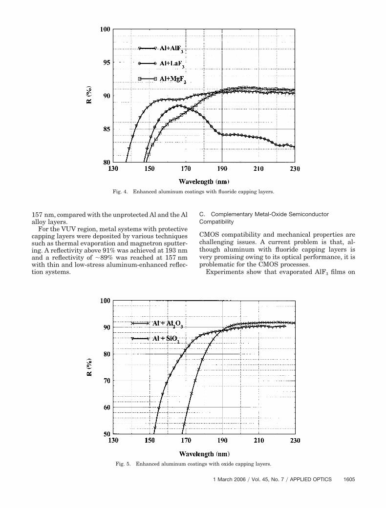
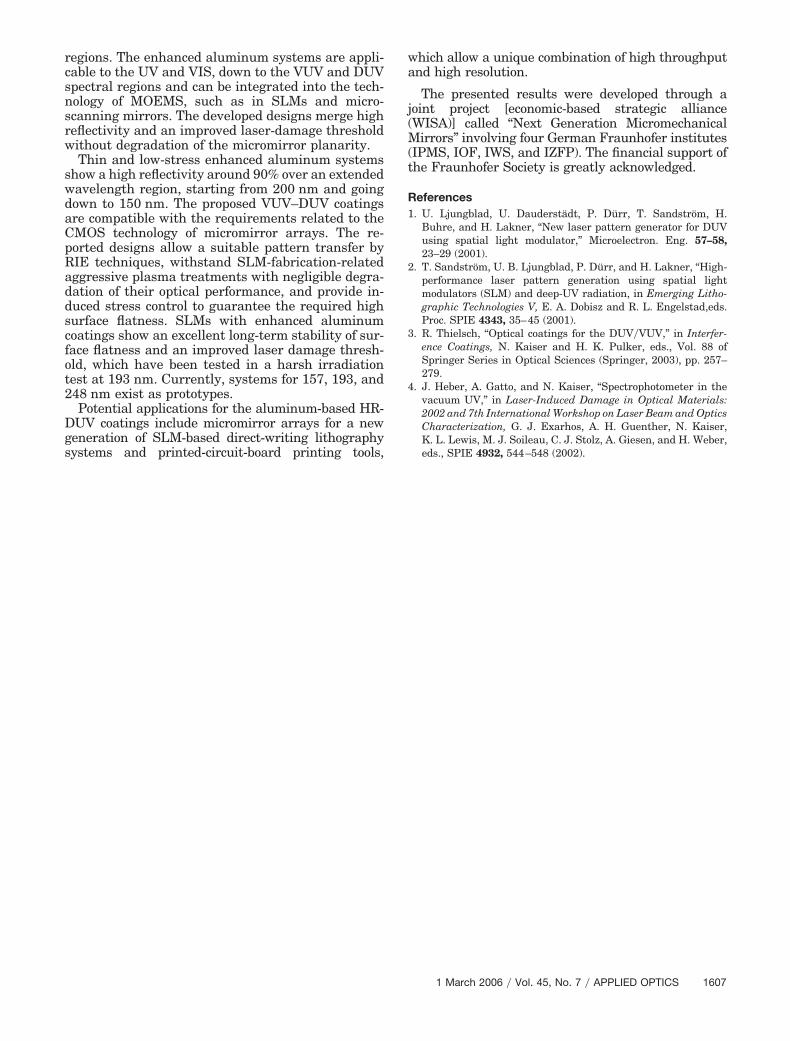
157 nm. To achieve this, we introduced a cappinglayer into the coating design to protect the alumi-num and to enhance the reflectance at the intendedwavelength. Thin films of fluoride or oxide evapo-rated immediately in the same vacuum cycle, juston top of a freshly deposited aluminum layer,thereby protecting the aluminum mirror againstfurther oxidation of the air. Fluoride materials�LaF3, AlF3, MgF2� and oxide materials �Al2O3, SiO2�were investigated as capping layers. The oxide andfluoride materials were analyzed to evaluate accu-mulated stresses and to extract optical and physicalcharacteristics to permit an optimized coating de-sign.3,4 Enhanced aluminum coatings, optimized forhigh DUV–VUV reflectance and low film stress,were deposited on silicon test substrates. A reflec-tivity above 91% was achieved at 193 nm and areflectivity of �89% was reached at 157 nm with thethin and low-stress aluminum-enhanced reflectionsystems (Fig. 3).
The total thickness of the enhanced aluminumcoatings with a protection layer is less than 150 nm,which minimizes deformation of the micromirrorsurface caused by the coating. As shown in Fig. 3, abroadband high reflectivity of nearly 90% wasreached over an extended wavelength region start-ing at 200 nm and going down to 150 nm, which is ofgreat interest for VUV applications at 193 and157 nm. The spectral reflectance of enhanced alu-minum coatings with fluoride capping layers andwith oxide capping layers is shown in more detail inFigs. 4 and 5.
Table 2 gives the reflectance values of the en-hanced aluminum coatings achieved at 193 and
Fig. 3. Enhanced aluminum system for 157 and 193 nm on the silicon substrate for comparison with the unprotected aluminum coating.R, reflectivity; total thickness, �100 nm; total stress, �150 Mpa.
157 nm, compared with the unprotected Al and the Alalloy layers.
For the VUV region, metal systems with protectivecapping layers were deposited by various techniquessuch as thermal evaporation and magnetron sputter-ing. A reflectivity above 91% was achieved at 193 nmand a reflectivity of �89% was reached at 157 nmwith thin and low-stress aluminum-enhanced reflec-tion systems.
C. Complementary Metal-Oxide SemiconductorCompatibility
CMOS compatibility and mechanical properties arechallenging issues. A current problem is that, al-though aluminum with fluoride capping layers isvery promising owing to its optical performance, it isproblematic for the CMOS processes.
Experiments show that evaporated AlF3 films on
Fig. 4. Enhanced aluminum coatings with fluoride capping layers.
Fig. 5. Enhanced aluminum coatings with oxide capping layers.
Al are porous. Contact with water (air humidity) re-sults in the appearance of bubbles under the coating.Therefore single AlF3 coatings are not acceptableeven though they are easily reactive ion etched (RIE)and CMOS compatible.
The MgF2 top coatings show high tensile strain.Therefore mirrors using Al�MgF2 as a top coatingwithout a compensation layer are deformed.
Single LaF3 layers show a small etch rate with theRIE technique, so they cannot be etched in a reason-able amount of time.
Furthermore, there is still an open question ofwhether the humidity-related film-stress instabilityintroduced by the porosity of all films leads to achange in mirror planarity under laser irradiation orunder a dry N2 environment, in which water couldgradually diffuse out of the films and tensile stresscould therefore increase again.
Table 3 shows the CMOS process compatibility ofthe different coatings. Although Al with the fluoridecapping layers is promising owing to its optical perfor-mance, its use is precluded by the previously men-tioned etch-process issues. Thus current developmentsfocus on the oxide capping layers.
D. Patterning and Laser Irradiation Tests
Patterning results show successfully structured mi-cromirror arrays with an optimized enhanced Al re-flector, confirming a good pattern transfer anduniformity. The deformation of the mirror plate wasmeasured by interferometry. The excellent planarityof an optimized multilayer mirror composed of an Alalloy base and an enhanced Al reflective coating isdemonstrated before and after laser irradiation bytwo randomly chosen individual mirrors in Fig. 6.
In this particular layout the mirror has a centralsupport post and plate dimensions of 16 �m �16 �m. The small mean deformation stayed almostconstant during the laser irradiation test. It reducedfrom 3.0 nm before and 2.3 nm after laser irradia-tion. Single-layer micromirrors made from the stan-dard Al alloy showed a significant deformation as aconsequence of the laser test. Hence the enhanced Altop coating increases the long-term stability of Alalloy micromirrors by mechanically stabilizing theirsurfaces.
5. Conclusion
Highly reflective low-stress optical coatings formicromechanical mirrors have been developed forMOEMS applications in the DUV and VUV spectral
Fig. 6. Interferometric surface topography of an optimized 16 �m � 16 �m multilayer micromirror with a center post before (left) and after (right)the laser irradiation test. The rms deformation of the free-standing multilayer mirror is 3.0 nm before and 2.3 nm after laser irradiation with an ArFexcimer laser (wavelength, 193 nm; 107 pulses; pulse duration, 12 ns; pulse energy, 100 �J�cm2).
Table 2. Reflectance of Enhanced Aluminum Coatings forMicromirror Arrays
CoatingSystem Deposition Technique
R at � �193 nm (%)
R at � �157 nm (%)
Al alloy dc magnetron sputtering 75–80 –Al Evaporation 88 73.4Al dc magnetron sputtering 88 71Al�AlF3 Evaporation 90.9 89Al�MgF2 Evaporation 91.6 88Al�LaF3 Evaporation 84 88.4Al�Al2O3 Evaporation 90.8 –Al�SiO2 Evaporation 89.2 60
Table 3. CMOS Process Compatibility of the Different Coatingsa
regions. The enhanced aluminum systems are appli-cable to the UV and VIS, down to the VUV and DUVspectral regions and can be integrated into the tech-nology of MOEMS, such as in SLMs and micro-scanning mirrors. The developed designs merge highreflectivity and an improved laser-damage thresholdwithout degradation of the micromirror planarity.
Thin and low-stress enhanced aluminum systemsshow a high reflectivity around 90% over an extendedwavelength region, starting from 200 nm and goingdown to 150 nm. The proposed VUV–DUV coatingsare compatible with the requirements related to theCMOS technology of micromirror arrays. The re-ported designs allow a suitable pattern transfer byRIE techniques, withstand SLM-fabrication-relatedaggressive plasma treatments with negligible degra-dation of their optical performance, and provide in-duced stress control to guarantee the required highsurface flatness. SLMs with enhanced aluminumcoatings show an excellent long-term stability of sur-face flatness and an improved laser damage thresh-old, which have been tested in a harsh irradiationtest at 193 nm. Currently, systems for 157, 193, and248 nm exist as prototypes.
Potential applications for the aluminum-based HR-DUV coatings include micromirror arrays for a newgeneration of SLM-based direct-writing lithographysystems and printed-circuit-board printing tools,
which allow a unique combination of high throughputand high resolution.
The presented results were developed through ajoint project [economic-based strategic alliance(WISA)] called “Next Generation MicromechanicalMirrors” involving four German Fraunhofer institutes(IPMS, IOF, IWS, and IZFP). The financial support ofthe Fraunhofer Society is greatly acknowledged.
References1. U. Ljungblad, U. Dauderstädt, P. Dürr, T. Sandström, H.
Buhre, and H. Lakner, “New laser pattern generator for DUVusing spatial light modulator,” Microelectron. Eng. 57–58,23–29 (2001).
2. T. Sandström, U. B. Ljungblad, P. Dürr, and H. Lakner, “High-performance laser pattern generation using spatial lightmodulators (SLM) and deep-UV radiation, in Emerging Litho-graphic Technologies V, E. A. Dobisz and R. L. Engelstad,eds.Proc. SPIE 4343, 35–45 (2001).
3. R. Thielsch, “Optical coatings for the DUV�VUV,” in Interfer-ence Coatings, N. Kaiser and H. K. Pulker, eds., Vol. 88 ofSpringer Series in Optical Sciences (Springer, 2003), pp. 257–279.
4. J. Heber, A. Gatto, and N. Kaiser, “Spectrophotometer in thevacuum UV,” in Laser-Induced Damage in Optical Materials:2002 and 7th International Workshop on Laser Beam and OpticsCharacterization, G. J. Exarhos, A. H. Guenther, N. Kaiser,K. L. Lewis, M. J. Soileau, C. J. Stolz, A. Giesen, and H. Weber,eds., SPIE 4932, 544–548 (2002).