Page 1
Majlesi Journal of Electrical Engineering Vol. 14, No. 2, June 2020
1
High Performance Low Latency 16×16 bit Booth Multiplier
using Novel 4-2 Compressor Structure
Ali Rahnamaei1*, Azadeh Kiani Sarkaleh2
1- Department of Electrical Engineering, Ardabil Branch, Islamic Azad University, Ardabil, Iran.
Email: [email protected] (Corresponding author)
2- Department of Electrical Engineering, Rasht Branch, Islamic Azad University, Rasht, Iran.
Email: [email protected]
Received: May 2019 Revised: September 2019 Accepted: November 2019
ABSTRACT:
In this article, the design procedure of a low latency Booth multiplier has been proposed. With the help of a novel 4-2
compressor, a high-performance 16×16 bit Booth multiplier has been implemented, which depicts high operating
frequency. To achieve this, the proposed 4-2 compressor has been utilized successively in the Partial Product
Reduction Tree (PPRT) of the multiplier and by means of radix-4 Booth scheme, the multiplier has been designed.
The Partial Product (PP) generation circuitry is also based on the other work published by the authors which enables
the designed structure to work at the frequency of 350MHz. The main advantage of the designed compressor is the
elimination of the middle stage inverters between cascaded blocks of PPRT which considerably enhances the speed of
whole system. Simulation results for TSMC 0.18µm CMOS technology and 1.8V power supply have been
demonstrated to confirm the correct operation of proposed 4-2 compressor. According to the results, the achieved
delay of the critical path for hard test and high capacitive load, equal to 100fF, is 936ps while a power consumption of
255.15µW has been achieved at the operating frequency of 100MHZ.
KEYWORDS: Booth Multiplier, Modified Booth Encoding Scheme, 4-2 Compressor, Radix-4, Low Latency.
1. INTRODUCTION
A comprehensive literature review depicts that
hardware implementation of binary multipliers contains
a history of 50 years. On the other hand,
implementation of algorithmic based multipliers has
been launched in 1970s [1] which was right after the
presentation of Booth [2], Wallace [3], and Dadda [4]
multiplication algorithms. In modern terminology, this
classification of multipliers which are based on a
specific multiplication procedure is recognized as
parallel multipliers.
Parallel multipliers and their successors, Booth
multipliers, are extremely utilized in high performance
communication systems such as Digital Signal
Processors (DSPs) and microprocessors. In spite of
high throughputs, the critical path delay in most of such
systems belongs to the multiplier. Hence, the speed
performance of whole structure is directly determined
by the parallel multiplier used in the architecture of the
system [5].
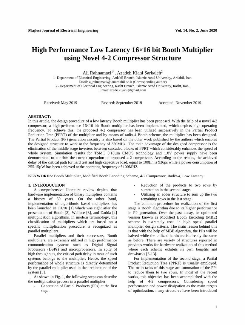
As shown in Fig. 1, the following steps can describe
the multiplication process in a parallel multiplier:
- Generation of Partial Products (PPs) at the first
step.
- Reduction of the products to two rows by
summation in the second stage.
- Utilizing an adder structure to sum up the two
remaining rows in the last stage.
The common procedure for realization of the first
stage is Booth algorithm due to its higher performance
in PP generation. Over the past decay, its optimized
version known as Modified Booth Encoding (MBE)
scheme is extremely used in high speed parallel
multiplier design criteria. The main reason behind this
is that with the help of MBE algorithm, the PPs will be
halved while the utilized hardware is already the same
as before. There are variety of structures reported in
previous works for hardware realization of this method
where each scheme exhibits its own benefits and
drawbacks [6-13].
For implementation of the second stage, a Partial
Product Reduction Tree (PPRT) is usually employed.
The main tasks of this stage are summation of the PPs
to reduce them to two rows. In most of the recent
works, this objective has been accomplished with the
help of 4-2 compressors. Considering speed
performance and power dissipation as the main targets
of optimization, many structures have been introduced
Page 2
Majlesi Journal of Electrical Engineering Vol. 14, No. 2, June 2020
2
for hardware realization of 4-2 and higher order
compressors where the emphasis was on behavioral
improvement of 4-2 compressors [14-19].
Fig. 1. Conventional scheme of a parallel multiplier.
For speed enhancement, Pass-Transistor Logic
(PTL) has been employed in [14]. However, the gate
level delay from inputs to the outputs was not reduced
to less than 4 XOR logic gates. On the other hand,
optimization of power was the main objective in [15].
Although these two circuits have shown better speed
performance compared to the previous works, in 2012,
two novel structures were reported in [16] and [17]
which surpassed the other works from the viewpoint of
gate level latency. Those architectures could achieve
the gate level delay about 2 XOR logic gates by
applying some modifications to the general truth table
of 4-2 compressor. The recent works reported in [18]
and [19], again worked on the optimization of power
consumption considering new aspects such as
approximate compressors.
At the final stage which pertains to the summation
of two remaining rows, there are efficient adding
configurations such as Carry-Lookahead Adder (CLA),
Carry Select Adder (CSA), Ripple Carry Adder (RCA),
and etc which can perform the task successively to
finalize the multiplication process.
Taking into account that the speed improvement for
4-2 compressor is the main objective in this paper, a
new scheme has been proposed which can achieve the
gate level delay of 2.25 XOR logic gates. The main
idea behind the implementation of this circuit is its
compatibility with the 4-2 compressor designed in [16]
which enables us to construct a high performance
PPRT. In order to evaluate the correct operation of the
proposed PPRT, a 16×16 bit booth multiplier has been
implemented. It must be mentioned that all of the
circuits have been designed employing TSMC 0.18µm
CMOS technology.
The paper is structured in following sections.
Implementation of the proposed 4-2 compressor has
been explained in section 2 while the important design
considerations have been clarified for the compatibility
between cascading of compressors. Section 3 illustrates
the design of the 16×16 bit booth multiplier consisting
of MBE scheme, PPRT and CSA. The simulation
results and the comparison with previous works have
been provided in section 4. Eventually, the conclusions
are discussed in section 5.
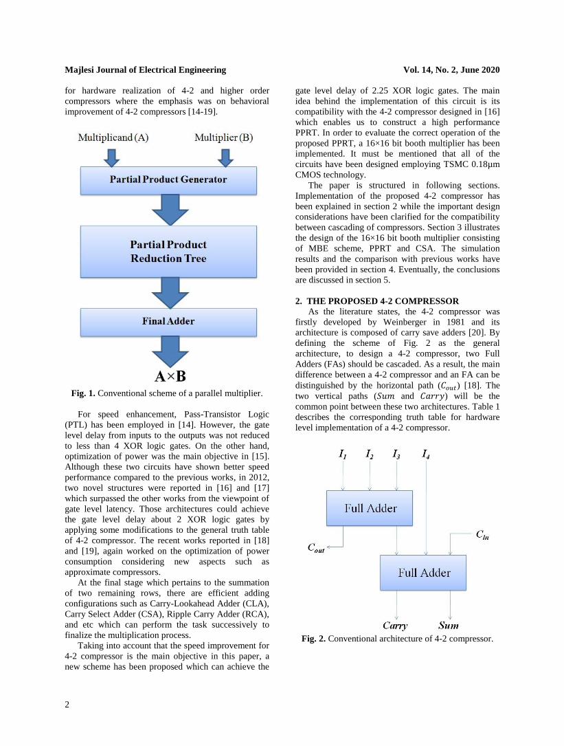
2. THE PROPOSED 4-2 COMPRESSOR
As the literature states, the 4-2 compressor was
firstly developed by Weinberger in 1981 and its
architecture is composed of carry save adders [20]. By
defining the scheme of Fig. 2 as the general
architecture, to design a 4-2 compressor, two Full
Adders (FAs) should be cascaded. As a result, the main
difference between a 4-2 compressor and an FA can be
distinguished by the horizontal path (𝐶𝑜𝑢𝑡) [18]. The
two vertical paths (𝑆𝑢𝑚 and 𝐶𝑎𝑟𝑟𝑦) will be the
common point between these two architectures. Table 1
describes the corresponding truth table for hardware
level implementation of a 4-2 compressor.
Fig. 2. Conventional architecture of 4-2 compressor.
Page 3
Majlesi Journal of Electrical Engineering Vol. 14, No. 2, June 2020
3
Table 1. General truth table of 4-2 compressor.
𝒏 𝑪𝒊𝒏 𝑪𝒐𝒖𝒕 𝑪𝒂𝒓𝒓𝒚 𝑺𝒖𝒎
0 0 0 0 0
1 0 0 0 1
2 0 - - 0
3 0 1 0 1
4 0 1 1 0
0 1 0 0 1
1 1 0 1 0
2 1 - - 1
3 1 1 1 0
4 1 1 1 1
Investigation of conventional truth table depicts that
there are two neutral states for 𝐶𝑜𝑢𝑡 and 𝐶𝑎𝑟𝑟𝑦 outputs
and these states exactly happen when two of four input
bits (𝐼1, 𝐼2, 𝐼3 and 𝐼4) in Fig. 2 have logical value of
one. The authors of [16] and [17] have assumed some
conditions for these two states which led to the
simplification of this table. The result of this effort was
two high speed circuits which show gate level delay
equal to almost 2 XOR logic gates from inputs to the
outputs while the structure reported in [16] which is
shown in Fig. 3 has better speed performance.
However, in Fig. 3, all of the outputs have been
obtained in complementary state. Therefore, an inverter
gate after each output is needed so that the real state of
the outputs can be achieved. Therefore, the real gate
level delay will increase to 2.5 XOR logic gates.
To solve this problem, the need for a compatible
structure becomes necessary so that the corresponding
inputs of such structure can operate in complementary
state. This was the motif for implementation of a novel
4-2 compressor in which its inputs are driven in
complementary mode. With the help of such
configuration, there is no need for any inverters at
output nodes of Fig. 3 which maintains the high-speed
performance of the circuit.
The proposed architecture has been shown in Fig. 4
where all of the inputs are in complementary state. By
defining the control signals 𝐸 and 𝐹 as:
𝐸 = (𝐼1 ⊕ 𝐼2) ⊕ (𝐼3 ⊕ 𝐼4) (1)
𝐹 = 𝐼1̅ + 𝐼2̅ + 𝐼3̅ + 𝐼4̅̅̅ ̅̅ ̅̅ ̅̅ ̅̅ ̅̅ ̅̅ ̅̅ ̅̅ ̅̅ (2)
the 𝐶𝑎𝑟𝑟𝑦 output will abide by:
Fig. 3. 4-2 compressor designed in [16].
Fig. 4. The proposed 4-2 compressor.
Page 4
Majlesi Journal of Electrical Engineering Vol. 14, No. 2, June 2020
4
𝐶𝑎𝑟𝑟𝑦 = (𝐸. 𝐶𝑖𝑛. 𝐹) + 𝐹 (3)
Furthermore, based on Table 1, if at least 2 of inputs
are equal to logic “1” value, then 𝐶𝑜𝑢𝑡 will rise to high
logic level. Finally, for the 𝑆𝑢𝑚 output we have:
𝑆𝑢𝑚 = (𝐼1 ⊕ 𝐼2) ⊕ (𝐼3 ⊕ 𝐼4) ⊕ 𝐶𝑖𝑛 (4)
To calculate the gate level delay for proposed
circuit, as Fig. 4 demonstrates, a latency of 2 XOR
logic gates plus one transistor is expectable.
Furthermore, by defining the latency of channel-ready
transistor equal to 0.25, then the latency can be
considered as 2.25 XOR logic gates.
3. THE MULTIPLIER
To show the efficiency of proposed 4-2 compressor
in conjunction with its compatibility with 4-2
compressor of Fig. 3, a 16×16 bit Booth multiplier
utilizing the MBE scheme of [22] (which was
previously designed and published by the authors), has
been implemented.
Fig. 5 shows the proposed concept for
implementation of such multiplier in which an MBE
scheme along with two cascaded 4-2 compressor
structures should be utilized to generate two rows of
bits for final addition. The final adder will sum these
rows so that the final product can be obtained.
Fig. 5. Proposed concept for implementation of 16×16
bit Booth multiplier.
To achieve this, the circuitry of MBE was
redesigned in CMOS 0.18µm technology considering
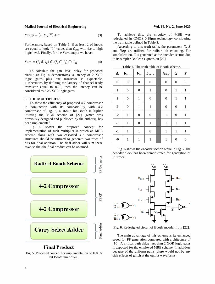
the truth table defined in Table 2.
According to this truth table, the parameters 𝑋, 𝑍
and 𝑁𝑒𝑔 are utilized for radix-4 bit encoding. For
simplification, �̅� is generated at the encoder section due
to its simpler Boolean expression [22].
Table 2. The truth table of Booth scheme.
𝒅𝒊 𝒃𝟐𝒊+𝟏 𝒃𝟐𝒊 𝒃𝟐𝒊−𝟏 𝑵𝒆𝒈 𝑿 𝒁
0 0 0 0 0 0 0
1 0 0 1 0 1 1
1 0 1 0 0 1 1
2 0 1 1 0 0 1
-2 1 0 0 1 0 1
-1 1 0 1 1 1 1
-1 1 1 0 1 1 1
-0 1 1 1 1 0 0
Fig. 6 shows the encoder section while in Fig. 7, the
decoder block has been demonstrated for generation of
PP rows.
Fig. 6. Redesigned circuit of Booth encoder from [22].
The main advantage of this scheme is its enhanced
speed for PP generation compared with architecture of
[10]. A critical path delay less than 2 XOR logic gates
is expected for the employed MBE scheme. In addition,
because of the uniform paths, there would not be any
side effects of glitch at the output waveforms.
Page 5
Majlesi Journal of Electrical Engineering Vol. 14, No. 2, June 2020
5
Fig. 7. Redesigned circuit of Booth decoder from [22].
Following the concept of achieving higher
operating frequency, CSA has been employed at the
final addition stage to sum the final remaining rows
[23]. Fig. 8 shows the basic structure used for
implementation of CSA architecture which utilizes four
bit adders.
Fig. 8. Employed CSA for implementation of final
adder.
As shown in Fig. 8, two 4-bit adder blocks are
employed in the structure of CSA. One of the adders
presumes that the input carry value is zero, while the
other considers the logic value of one for the input
carry. The carry outputs of these blocks are multiplexed
together to produce the final carry output of the
architecture. The multiplexing is performed by
selecting which adder contains the accurate value.
In addition, Fig. 9 illustrates the architecture of FA
utilized in the configuration of CSA in which Fig. 9(a)
presents the proposed circuit and Fig. 9(b) shows the
modified structure. To avoid cascading of the
multiplexers in CSA arrays which degrades the speed
performance, for odd FA cells, the proposed circuit of
Fig. 9(a) has been used while for even cells the
modified structure of Fig. 9(b) was employed.
Considering that the first eight bits along with the
last four bits of multiplication process in the
implemented 16×16 bit multiplier can be created at the
PPRT, the proposed architecture of CSA for summation
of twenty bits has been shown in Fig. 10.
0
1
0
1
Sum
Carry
A
B
A
B
A
B
Cin
Cin
(a)
0
1
0
1
Sum
Carry
A
B
A
B
A
B
Cin
Cin
Sum
Carry
(b)
Fig. 9. Proposed FA scheme (a) main circuit (b)
modified circuit.
Finally, Fig. 11 illustrates the scheme of
multiplication in which for the middle stages, the
cascaded 4-2 compressors are the structures shown in
Fig. 3 and Fig. 4, respectively. As described above, the
first eight bits and the last four bits can be computed in
the PPRT.
Therefore, the delay of critical path can be
calculated by means of the following relation:
𝑇𝑑𝑒𝑙𝑎𝑦 = 𝑡𝐵𝑜𝑜𝑡ℎ + 𝑡𝐶𝑜𝑚𝑝1 + 𝑡𝐶𝑜𝑚𝑝2 + 𝑡𝐴𝑑𝑑𝑒𝑟 (5)
In which, 𝑡𝐵𝑜𝑜𝑡ℎ describes the latency for
generation of PPs by MBE structure. In addition,
𝑡𝐶𝑜𝑚𝑝1 defines the propagation delay for 4-2
compressor shown in Fig. 3, while 𝑡𝐶𝑜𝑚𝑝2 represents
the latency associated with 4-2 compressor of Fig. 4.
Finally, 𝑡𝐴𝑑𝑑𝑒𝑟 denotes the delay of final addition
which is implemented by means of FAs.
Page 6
Majlesi Journal of Electrical Engineering Vol. 14, No. 2, June 2020
6
Fig. 10. The scheme of implemented CSA for 20 bit addition.
Fig. 11. The scheme of proposed 16×16 bit Booth multiplier.
It must be mentioned that in (5), the loading of each
block will directly affect the latency of its previous
level and it has been considered for accurate
measurement of propagation delay in the proposed
multiplier.
4. SIMULATION RESULTS AND COMPARISON
In order to investigate the correct operation of
proposed 4-2 compressor and obtain the delay of the
critical path, simulations using HSPICE for TSMC
standard 0.18µm CMOS technology and 1.8V power
supply were performed in which all of the outputs were
followed with high capacitive loads equal to 100fF.
Moreover, to perform a hard test for the designed
circuitry, the arrangement of the input bits was set in a
way so that the critical path will surely be enabled.
Fig. 12 depicts the result which confirms the
accurate operation of implemented structure. It must be
mentioned that the obtained delay which is equal to
936ps has been obtained for the high capacitive load
mentioned before. Moreover, the power consumption at
the operating frequency of 100MHz was 255.15 µW.
Page 7
Majlesi Journal of Electrical Engineering Vol. 14, No. 2, June 2020
7
Fig. 12. Simulation results for delay calculation of proposed compressor.
For a fair comparison between proposed 4-2
compressor and the previously reported works, the
compressor architectures of [14], [15], [16] and [17]
were also redesigned employing the gates used for
implementation of our circuitry.
These works are then simulated considering the
same conditions mentioned above. Based on the results
which have been presented in Fig. 13 and Fig. 14, the
delay of proposed compressor is lower than the
previous works while the power consumption is
favorably comparable with those works.
Considering the obtained results from simulations,
Table 3 illustrates the comparison of the proposed work
with previous designs. It must be mentioned that the
results for [16] has been obtained considering one
inverter cascading at the output nodes. Hence, the
lowest latency will belong to the proposed structure.
Finally, to obtain the delay of the critical path for
the proposed 16×16 bit multiplier, the layout of the
proposed multiplier was drawn by means of TSMC
0.18µm CMOS technology file where it is shown in
Fig. 15.
Fig. 13. Delay comparison of proposed work and
previous designs.
Fig. 14. The comparison of power dissipation between
proposed work and previous designs.
Table 3. Comparison of the proposed work and
previous designs
Work Proposed [14] [15] [16] [17]
Technology
(µm) 0.18 0.18 0.18 0.18 0.18
Transistor
Count 68 64 60 74 70
Gate Level
Delay (XOR)
2.25
gates
4
gates
3
gates
2.5
gates
2.25
gates
Power (µW)
@100MHz 255.15 248.4 193.2 296.9 262.1
Delay(ps) 936 1210 1150 978 953
An active area equal to 197µm× 289µm is
consumed for the whole architecture. After that, the
parasitics were extracted, post-layout simulations using
HSPICE for TSMC standard 0.18µm CMOS
technology and 1.8V power supply were carried out for
the designed multiplier architecture.
Page 8
Majlesi Journal of Electrical Engineering Vol. 14, No. 2, June 2020
8
Fig.15. Layout of the proposed 16×16 bit Booth multiplier.
Table 4 summarizes the obtained results for
propagation delay of implemented multiplier along
with the corresponding latencies of different blocks
utilized for realization of the multiplier. Based on the
results, the total latency of the proposed multiplier is
equal to 2841ps which confirms that the implemented
architecture can operate at the frequencies up to
351MHz if no pipeline stage is utilized for the speed
enhancement.
Table 4. Propagation delay based on post-layout
simulation results for the proposed multiplier and its
building blocks.
MBE Structure 255ps
4-2 compressor of Fig. 3 237ps
4-2 compressor of Fig. 4 249ps
Final Adder 2100ps
Total Latency 2841ps
Meanwhile, according to the results, the summation
of four latencies obtained for MBE structure, 4-2
compressors, and the final adder, will exactly become
equal to the obtained value for the total latency of the
proposed multiplier. This also complies with the
obtained value in (5).
It must be mentioned that for the pipeline
implementation of this structure much higher operating
frequencies are expected, since the clocked feature of
pipeline architecture will enable the subsections to
operate up to their own frequency limits. For instance,
the proposed 4-2 compressor can work in the frequency
of 1GHz even for high capacitive loads.
Moreover, the differences between the obtained
delays of the compressors in Table 3 and Table 4 are
due to the different capacitive loads. For the results of
Table 3, high capacitive load is used for hard test which
significantly increases the latency.
5. CONCLUSION
A novel architecture for 4-2 compressor has been
proposed in this paper which demonstrates excellent
speed performance. Having the compatibility feature
with 4-2 compressor circuit reported in [16], the
designed structure can successively be cascaded with
that circuit to construct a high speed PPRT for
utilization in high performance parallel multipliers.
Considering the fact that total transistor count of the
proposed 4-2 compressor is almost the same as
previous works, its active area consumption will have
no significant difference compared with those
structures.
Based on the simulation results for TSMC 0.18µm
CMOS technology and 1.8V power supply, the
obtained delays of the proposed 4-2 compressor for
normal and high capacitive loads are 249ps and 936ps,
respectively.
In addition, the designed Booth multiplier which is
based on PPRT consisting of combined 4-2
compressors can operate at the frequencies up to
351MHz.
Page 9
Majlesi Journal of Electrical Engineering Vol. 14, No. 2, June 2020
9
REFERENCES [1] AC Davies, and YT Fung, “Interfacing a Hardware
Multiplier to a General-purpose Microprocessor,” Microprocessors, Vol. 1, Issue 7, pp. 425-432,
October 1977.
[2] Andrew D. Booth, “A Signed Binary Multiplication
Technique,” The Quarterly Journal of Mechanics
and Applied Mathematics, Vol. IV, Pt. 2, 1951.
[3] C. S. Wallace, “A Suggestion for a Fast
Multiplier,” IEEE Transactions on Computers, Vol.
13, pp. 14-17, 1964.
[4] L. Dadda, “Some Schemes for Parallel
Multipliers,” Alta Frcquetiza, Vol. 34, pp. 349-356,
1965.
[5] Abu-Khater I.S., Bellaouar A. and Elmasry, M.I.,
“Circuit Techniques for CMOS Low-Power High-
Performance Multipliers,” IEEE Journal of Solid-
State Circuits, Vol. 31, Issue 10, pp. 1535-1546,
1996.
[6] Ohkubo N., Suzuki M., Shinbo T. et al., “A 4.4 ns
CMOS 54 54-b Multiplier Using Pass-Transistor
Multiplexer,” IEEE Journal of Solid-State Circuits,
Vol. 30, Issue 3, pp. 251-257, 1995.
[7] Wen-Chang Yeh and Chein-Wei Jen, “High-Speed
Booth Encoded Parallel Multiplier Design,” IEEE
Transactions on Computers, Vol. 49, No. 7, July
2000.
[8] Hsin-Lei Lin, Chang R.C. and Ming-Tsai Chan,
“Design of a Novel Radix-4 Booth Multiplier,” The
2004 IEEE Asia-Pacific Conference on Circuits and
Systems, Vol. 2, pp. 837-840, 2004.
[9] Shiann-Rong Kuang, Jiun-Ping Wang, and Cang-
Yuan Guo, “Modified Booth Multipliers With a
Regular Partial Product Array,” IEEE
Transactions on Circuits and Systems—II: Express
Briefs, Vol. 56, No. 5, pp. 404-408, May 2009.
[10] A. Fathi, S. Azizian, R. Fathi, H.G. Tamar, “Low
Latency, Glitch-Free Booth Encoder-Decoder for
High Speed Multipliers,” IEICE Electronics
Express, Vol. 9, No. 16, pp. 1335-1341, 2012.
[11] Fathi, S. Azizian, Kh. Hadidi, A. Khoei, “Ultra High
Speed Modified Booth Encoding Architecture for
High Speed Parallel Accumulations,” IEICE
transactions on electronics, Vol. 95, No. 4, pp. 706-
709, 2012.
[12] Honglan Jiang, Jie Han, Fei Qiao, and Fabrizio
Lombardi, “Approximate Radix-8 Booth
Multipliers for Low-Power and High-Performance
Operation,” IEEE Transactions on Computers, Vol.
65, No. 8, pp. 2638-2644, Aug 2016.
[13] Liu, Weiqiang, et al, “Design of Approximate
Radix-4 Booth Multipliers for Error-tolerant
Computing,” IEEE Transactions on Computers
2017.
[14] D. Radhakrishnan and A. P. Preethy, “Low-power
CMOS Pass Logic 4-2 Compressor for High-speed
Multiplication,” in Proc. 43rd IEEE Midwest Symp.
Circuits Syst., Vol. 3, 2000, pp. 1296–1298.
[15] Chip-Hong Chang, Jiangmin Gu, and Mingyan
Zhang, “Ultra Low-Voltage Low-Power CMOS 4-2
and 5-2 Compressors for Fast Arithmetic
Circuits,” IEEE Transactions on Circuits and
Systems I, Vol. 51, Issue 10, pp. 1985-1997, 2004.
[16] Amir Fathi, Sarkis Azizian, Khayrollah Hadidi and
Abdollah Khoei, “A Novel and Very Fast 4-2
Compressor for High Speed Arithmetic
Operations,” IEICE transactions on electronics, Vol.
E95-C, No. 4, April 2012.
[17] Amir Fathi, Sarkis Azizian, Khayrollah Hadidi,
Abdollah Khoei and Amin Chegeni, “CMOS
Implementation of a Fast 4-2 Compressor for
Parallel Accumulations,” 2012 IEEE International
Symposium on Circuits and Systems (ISCAS), pp.
1476-1479, May 2012.
[18] A. Momeni, J. Han, P.Montuschi, and F. Lombardi,
“Design and Analysis of Approximate
Compressors for Multiplication,” IEEE
Transactions on Computers, Vol. 64, No. 4, pp. 984-
994, 2015.
[19] Omid Akbari, Mehdi Kamal, Ali Afzali-Kusha, and
Massoud Pedram, “Dual-Quality 4:2 Compressors
for Utilizing in Dynamic Accuracy Configurable
Multipliers,” IEEE Transactions on Very Large
Scale Integration (VLSI) Systems, Vol. 25, No. 4, pp.
1352-1361, 2017.
[20] A. Weinberger, “4:2 Carry-Save Adder Module,”
IBM Technical Disclosure Bull., Vol. 23, Jan. 1981.
[21] Oklobdzija V.G., Villeger D., and Liu S.S., “A
Method for Speed Optimized Partial Product
Reduction and Generation of Fast Parallel
Multipliers using An Algorithmic Approach,” IEEE Transactions on Computers, Vol. 45, No. 3, pp.
294-306, Mar. 1996.
[22] A. Rahnamaei, G. Zare Fatin, A. Eskandarian, “High
Speed Radix-4 Booth Scheme in CNTFET
Technology for high Performance Parallel
Multipliers,” International Journal of Nano
Dimension, Vol. 10, No. 3, pp. 281-290. 2019.
[23] R.UMA, Vidya Vijayan, M. Mohanapriya, and
Sharon Paul, “Area, Delay and Power Comparison
of Adder Topologies,” International Journal of VLSI
design & Communication Systems (VLSICS), Vol. 3,
No. 1, February 2012.