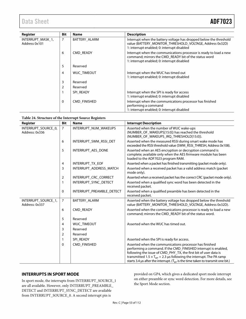
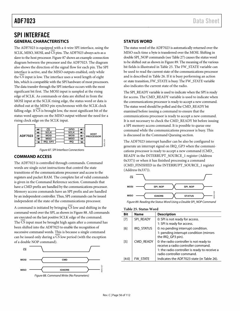
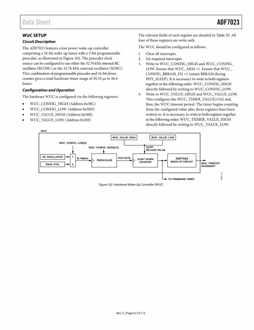
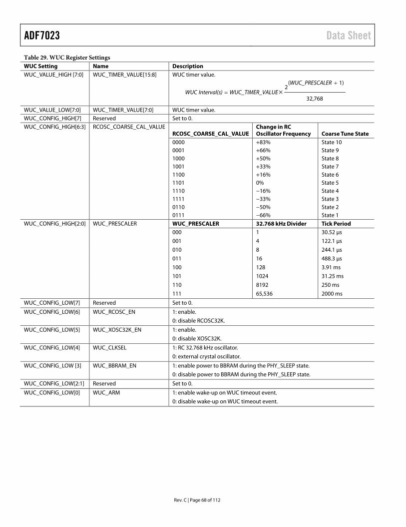
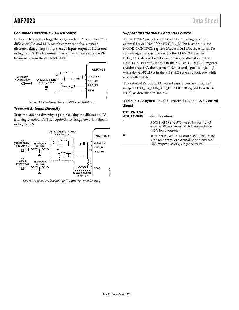
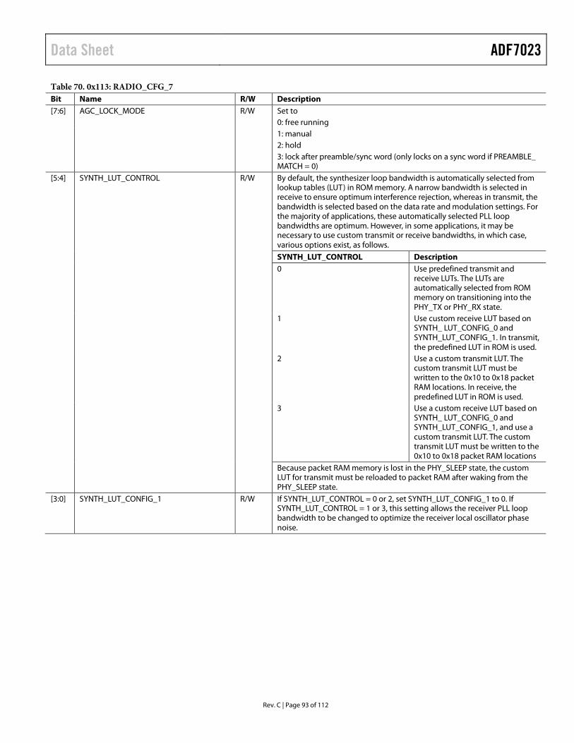
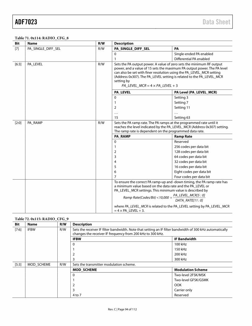
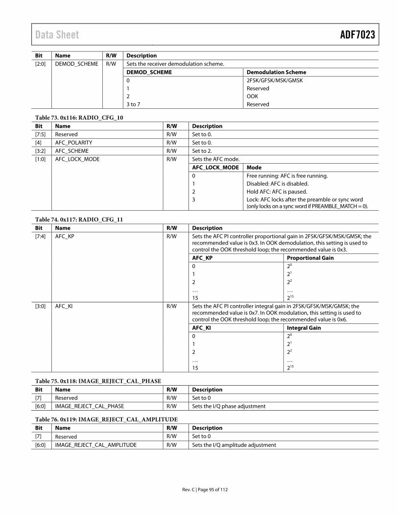
High Performance, Low Power, ISM Band FSK/GFSK/OOK/MSK/GMSK Transceiver IC
Data Sheet ADF7023
Rev. C Information furnished by Analog Devices is believed to be accurate and reliable. However, no responsibility is assumed by Analog Devices for its use, nor for any infringements of patents or other rights of third parties that may result from its use. Specifications subject to change without notice. No license is granted by implication or otherwise under any patent or patent rights of Analog Devices. Trademarks and registered trademarks are the property of their respective owners.
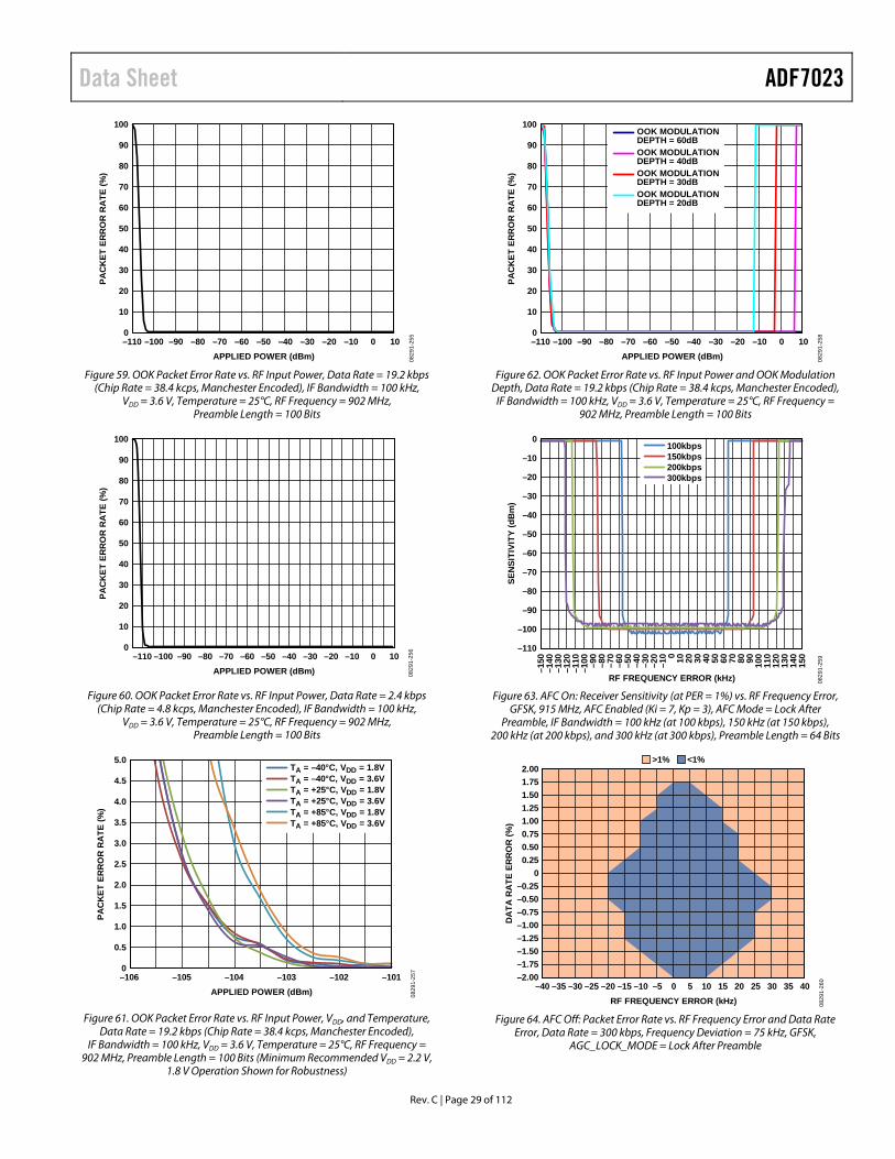
−116 dBm at 1.0 kbps, 2FSK, GFSK −107.5 dBm at 38.4 kbps, 2FSK, GFSK −102.5 dBm at 150 kbps, GFSK, GMSK −100 dBm at 300 kbps, GFSK, GMSK −104 dBm at 19.2 kbps, OOK
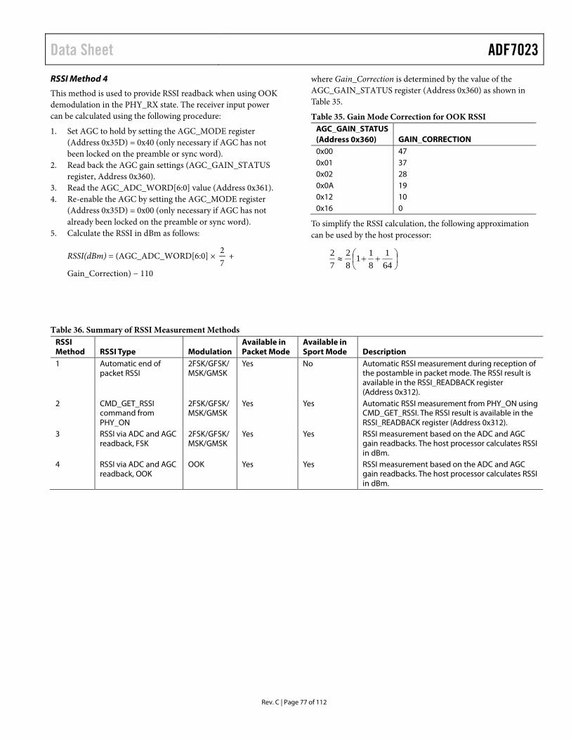
Very low power consumption 12.8 mA in PHY_RX mode (maximum front-end gain) 24.1 mA in PHY_TX mode (10 dBm output, single-ended PA) 0.75 µA in PHY_SLEEP mode (32 kHz RC oscillator active) 1.28 µA in PHY_SLEEP mode (32 kHz XTAL oscillator active) 0.33 µA in PHY_SLEEP mode (Deep Sleep Mode 1)
RF output power of −20 dBm to +13.5 dBm (single-ended PA) RF output power of −20 dBm to +10 dBm (differential PA) Patented fast settling automatic frequency control (AFC) Digital received signal strength indication (RSSI) Integrated PLL loop filter and Tx/Rx switch Fast automatic VCO calibration Automatic synthesizer bandwidth optimization On-chip, low-power, custom 8-bit processor
Radio control Packet management Smart wake mode
Packet management support Highly flexible for a wide range of packet formats Insertion/detection of preamble/sync word/CRC/address Manchester and 8b/10b data encoding and decoding Data whitening
Smart wake mode Current saving low power mode with autonomous receiver
wake up, carrier sense, and packet reception Downloadable firmware modules
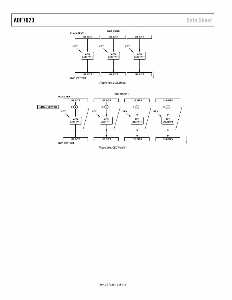
acceleration and key sizes of 128 bits, 192 bits, and 256 bits
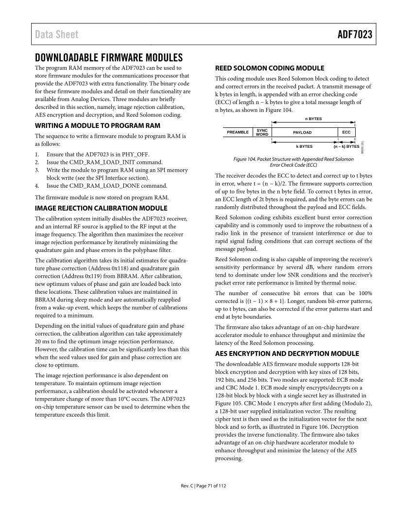
Reed Solomon error correction with hardware acceleration 240-byte packet buffer for TX/RX data Efficient SPI control interface with block read/write access Integrated battery alarm and temperature sensor Integrated RC and 32.768 kHz crystal oscillator On-chip, 8-bit ADC 5 mm × 5 mm, 32-pin, LFCSP package
APPLICATIONS Smart metering IEEE 802.15.4g Wireless MBUS Home automation Process and building control Wireless sensor networks (WSNs) Wireless healthcare
10, Issue 4• Industrial ICs Solutions Bulletin, Volume 10, Issue 8• RF Transceivers for Short Range DevicesTechnical Articles• Innovative Line Sensor Design with ADI Energy
Harvesting and Low Power Signal Chain• Low Power, Low Cost, Wireless ECG Holter Monitor• RF Meets Power Lines: Designing Intelligent Smart Grid
Systems that Promote Energy Efficiency• Smart Metering Technology Promotes Energy Efficiency
for a Greener World• The Use of Short Range Wireless in a Multi-Metering
System• Understand Wireless Short-Range Devices for Global
License-Free Systems• Wireless Short Range Devices and Narrowband
Communications• Wireless Technologies for Smart Meters: Focus on Water
Metering
Design Resources• ADF7023 Material Declaration• PCN-PDN Information• Quality And Reliability• Symbols and Footprints
DiscussionsView all ADF7023 EngineerZone Discussions
Sample and BuyVisit the product page to see pricing options
Technical SupportSubmit a technical question or find your regional support number
* This page was dynamically generated by Analog Devices, Inc. and inserted into this data sheet. Note: Dynamic changes to the content on this page does not constitute a change to the revision number of the product data sheet. This content may be frequently modified.
TABLE OF CONTENTS Features .............................................................................................. 1 Applications ....................................................................................... 1 Revision History ............................................................................... 3 Functional Block Diagram .............................................................. 4 General Description ......................................................................... 4 Specifications ..................................................................................... 6
RF and Synthesizer Specifications .............................................. 6 Transmitter Specifications ........................................................... 7 Receiver Specifications ................................................................ 9 Timing and Digital Specifications ............................................ 13 Auxilary Block Specifications ................................................... 14 General Specifications ............................................................... 15 Timing Specifications ................................................................ 16
Absolute Maximum Ratings .......................................................... 17 ESD Caution ................................................................................ 17
Pin Configuration and Function Descriptions ........................... 18 Typical Performance Characteristics ........................................... 20 Terminology .................................................................................... 32 Radio Control .................................................................................. 33
Radio States ................................................................................. 33 Initialization ................................................................................ 35 Commands .................................................................................. 35 Automatic State Transitions ...................................................... 37 State Transition and Command Timing .................................. 38
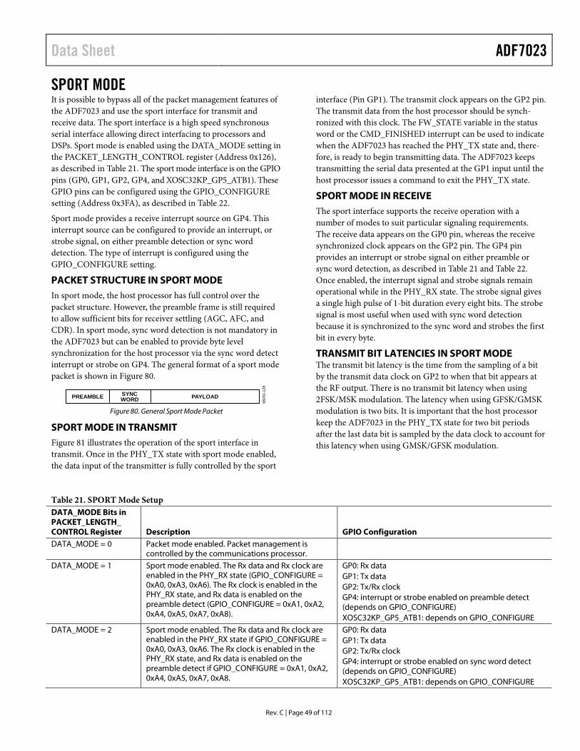
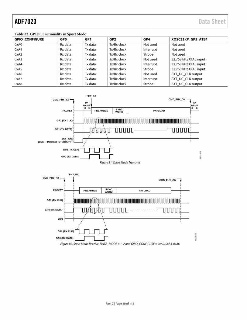
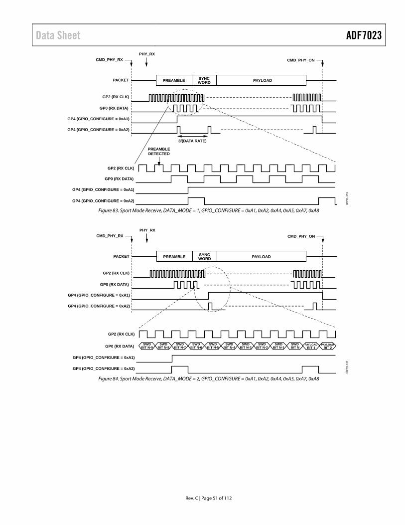
Sport Mode ...................................................................................... 49 Packet Structure in Sport Mode ............................................... 49 Sport Mode in Transmit ............................................................ 49 Sport Mode in Receive ............................................................... 49 Transmit Bit Latencies in Sport Mode ..................................... 49
REVISION HISTORY 7/12—Rev. B to Rev. C Changes to Features Section ............................................................ 1 Changed 1.8 V to 2.2 V, General Description Section ................. 4 Changed 1.8 V to 2.2 V, Table 1 Summary .................................... 6 Changed 1.8 V to 2.2 V, Table 2 ....................................................... 7 Changes to Table 3 ............................................................................ 9 Changes to Table 5 .......................................................................... 14 Changes to VDD Parameter, Table 6 ............................................... 15 Changes to Timing Specifications Section ................................... 16 Deleted t1 from Table 7, Figure 2, and Figure 3 ........................... 16 Changes to Table 9 .......................................................................... 18 Changes to Figure 5 to Figure 10 .................................................. 20 Changes to Figure 11, Figure 12 Caption, Figure 13 and Figure 14 Caption ............................................................................ 21 Changes to Figure 19 Caption to Figure 21 Caption .................. 22 Changes to Figure 26 Caption ....................................................... 23 Changes to Figure 34 Caption ....................................................... 24 Changes to Figure 61 Caption and Figure 64 Caption ............... 29 Changes to Figure 72 ...................................................................... 31 Changes to PHY_SLEEP Section .................................................. 33 Changes to Initialization After Application of Power Section, Initialization After Issuing the CMD_HW_RESET Command Section, Initialization on Transitioning from PHY_SLEEP (After CS Is Brought Low) Section, and Initialization After a WUC Timeout Section ................................................................... 35 Changes to CMD_RAM_LOAD_DONE (0xC7) Section ......... 37 Deleted CMD_SYNC (0xA2) Section .......................................... 37 Changes to State Transition and Command Timing Section .... 38 Changes to Table 11 and Table 12 ................................................. 39 Changes to Addressing Section ..................................................... 45 Changes to Example Address Check Section, Table 18, and CRC Section .............................................................................................. 46 Changes to Figure 79 ...................................................................... 47 Changes to Figure 81 and Figure 82 ............................................. 50 Changes to Figure 83 and Figure 84 ............................................. 51 Changes to CMD_FINISHED Description, Table 24................. 53 Changes to Command Access Section ......................................... 56 Changes to Figure 97 ...................................................................... 63 Changes to Table 29 ........................................................................ 68 Added Calibrating the RC Oscillator Section, Performing a Fine Calibration of the RC Oscillator Section, and Performing a Coarse Calibration of the RC Oscillator Section ........................ 69
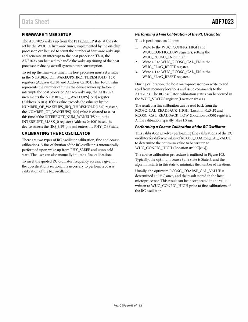
Added Figure 103; Renumbered Sequentially ............................. 70 Changes to Writing a Module to Program RAM Section .......... 71 Changes to Automatic PA Ramp Section Equation and Image Channel Rejection Section ............................................................. 75 Changes to Temperature Sensor Section and Table 43 .............. 83 Changes to Figure 110 .................................................................... 84 Changes to Figure 111 and Figure 112 ......................................... 85 Changes to Support for External PA and LNA Control Section and Table 45 ..................................................................................... 86 Changes to CMD_SYNC Description Column, Table 46.......... 87 Changes to Table 48 ........................................................................ 88 Changes to Table 49 ........................................................................ 89 Changes to SYNTH_LUT_CONTROL_1 Description Column, Table 70 ............................................................................................. 93 Changes to Table 78 ........................................................................ 96 Changes to Table 79 ........................................................................ 97 Changes to Table 84 and Table 86 ................................................. 98 Changes to Table 94 ........................................................................ 99 Added Table 95, Table 96, and Table 97; Renumbered Sequentially .................................................................................... 100 Changes to Table 101 .................................................................... 101 Added Table 124 and Table 125................................................... 105
3/11—Rev. A to Rev. B Changes to RSSI Method 3, Formula ........................................... 72 Changes to RSSI Method 4, Step 3 ................................................ 72 Changes to RSSI Method 4, Step 5 Formula and Formula Approximation ................................................................................ 73 Added Register 0x361 to Table 49 ................................................. 85 Added Table 129, Renumbered Subsequent Tables .................. 104
2/11—Rev. 0 to Rev. A Changes to Table 9, DGUARD Description ................................ 18 Changes to Sport Mode in Receive Section ................................. 47 Changes to Crystal Oscillator Section, Typical Crystal Load Capacitance Tuning Range Value, and to Table 31 ..................... 70 Changes to RSSI Method 3 Section .............................................. 72 Changes to RSSI Method 4 Section .............................................. 73 Changes to Table 41, 9.6 kbps and 1 kbps Data Rate Setup Values ..................................................................................... 78 Changes to Table 108, ADC_PD_N Description ...................... 100
8/10—Revision 0: Initial Version
ADF7023 Data Sheet
Rev. C | Page 4 of 112
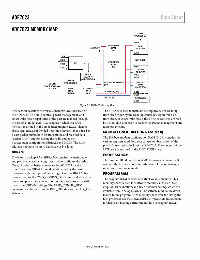
FUNCTIONAL BLOCK DIAGRAM
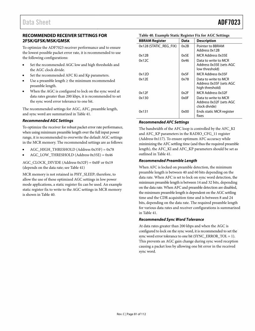
Figure 1.
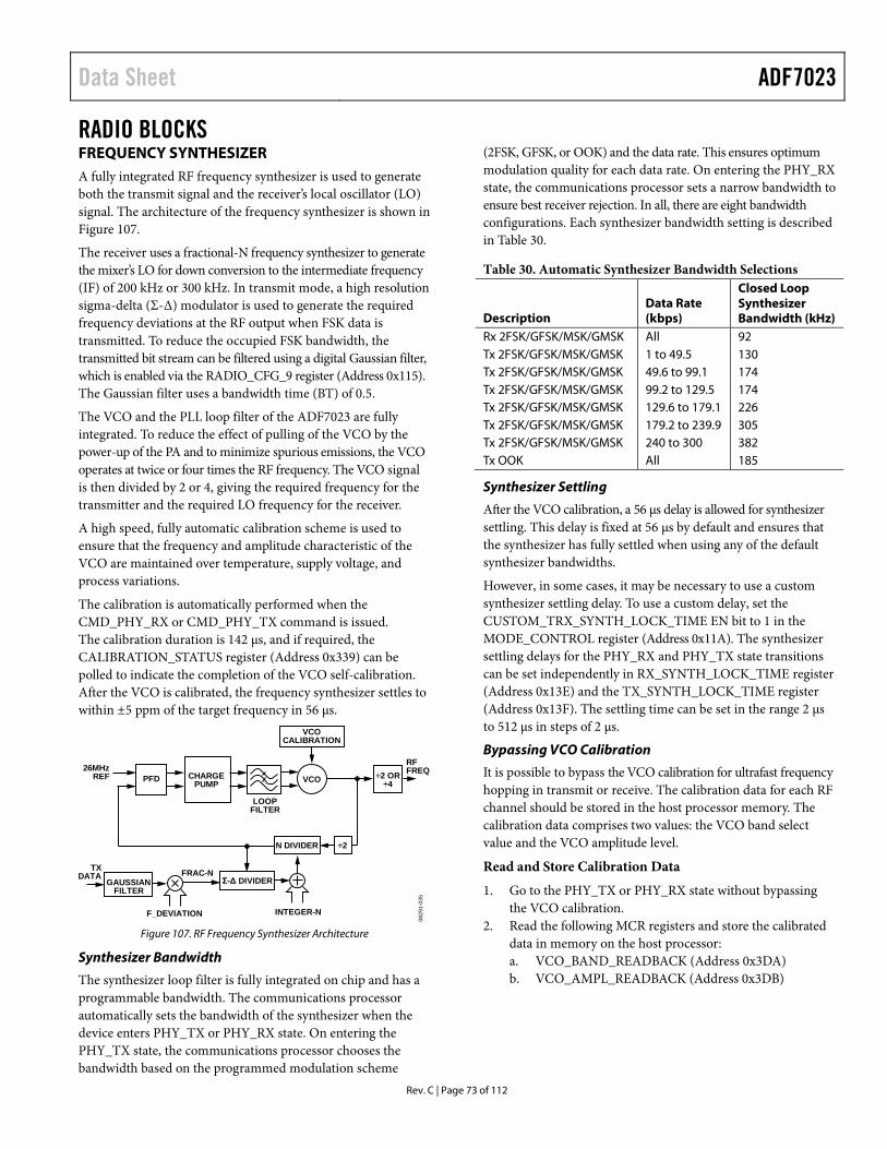
GENERAL DESCRIPTION The ADF7023 is a very low power, high performance, highly integrated 2FSK/GFSK/OOK/MSK/GMSK transceiver designed for operation in the 862 MHz to 928 MHz and 431 MHz to 464 MHz frequency bands, which cover the worldwide license-free ISM bands at 433 MHz, 868 MHz, and 915 MHz. It is suitable for circuit applications that operate under the European ETSI EN300-220, the North American FCC (Part 15), the Chinese short-range wireless regulatory standards, or other similar regional standards. Data rates from 1 kbps to 300 kbps are supported.
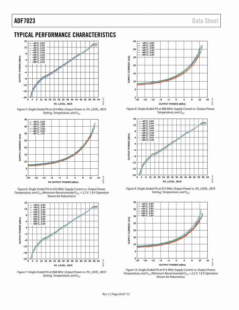
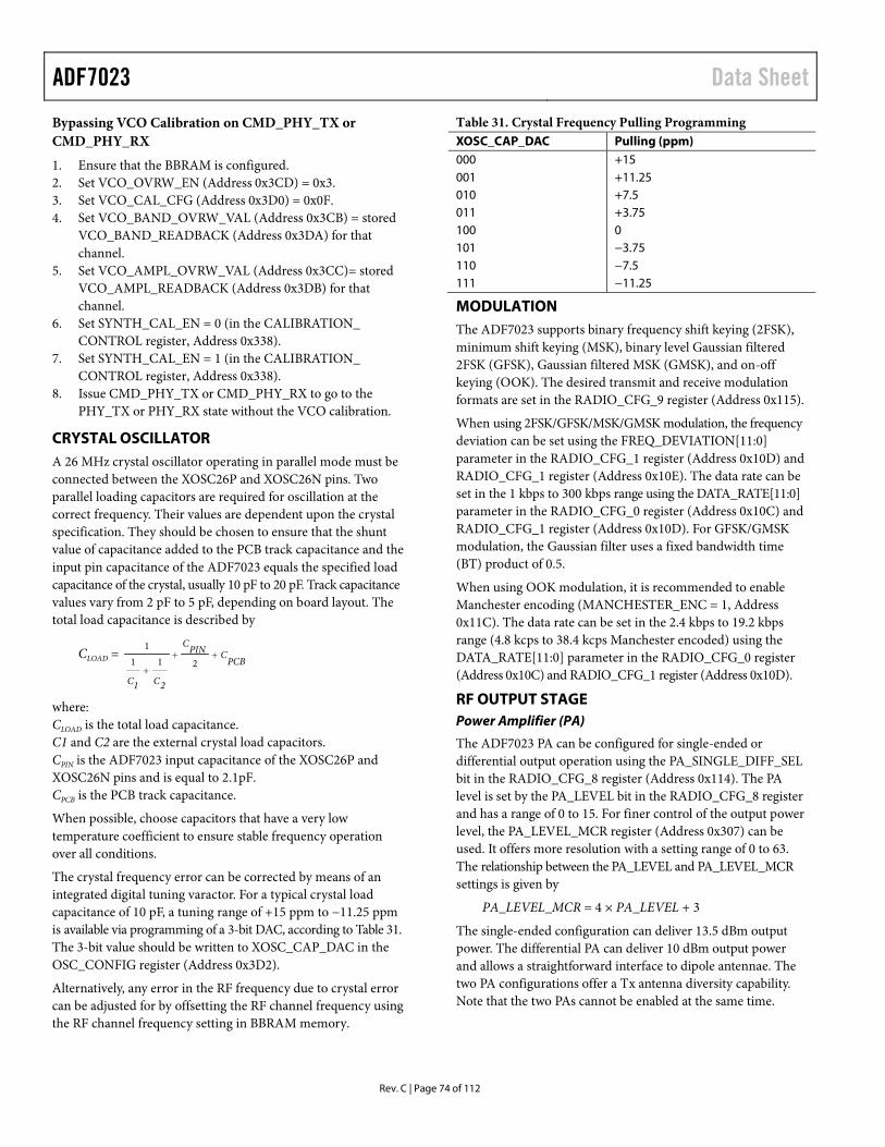
The transmit RF synthesizer contains a VCO and a low noise fractional-N PLL with an output channel frequency resolution of 400 Hz. The VCO operates at 2× or 4×, the fundamental frequency to reduce spurious emissions. The receive and transmit synthesizer bandwidths are automatically, and independently, configured to achieve optimum phase noise, modulation quality, and settling time. The transmitter output power is programmable from −20 dBm to +13.5 dBm, with automatic PA ramping to meet transient spurious specifications. The part possesses both single-ended and differential PAs, which allows for Tx antenna diversity.
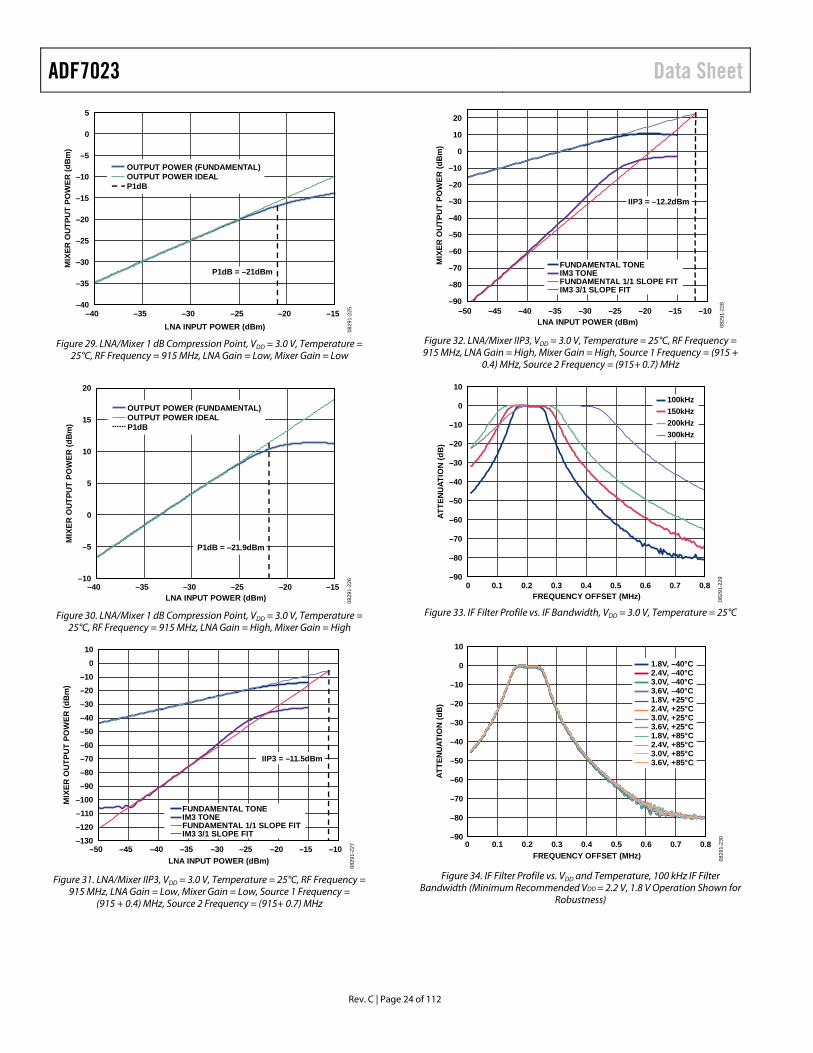
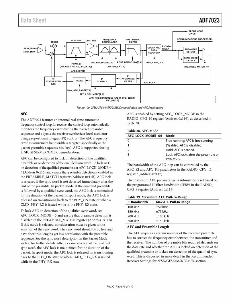
The receiver is exceptionally linear, achieving an IP3 specification of −12.2 dBm and −11.5 dBm at maximum gain and minimum gain, respectively, and an IP2 specification of 18.5 dBm and 27 dBm at maximum gain and minimum gain, respectively. The receiver achieves an interference blocking specification of 66 dB at ±2 MHz offset and 74 dB at ±10 MHz offset. Thus, the part is extremely resilient to the presence of interferers in spectrally noisy environments. The receiver features a novel, high speed, automatic frequency control (AFC) loop, allowing the PLL to find and correct any RF frequency errors in the recovered packet.
A patent pending, image rejection calibration scheme is available through a program download. The algorithm does not require the use of an external RF source nor does it require any user intervention once initiated. The results of the calibration can be stored in nonvolatile memory for use on subsequent power-ups of the transceiver.
The ADF7023 operates with a power supply range of 2.2 V to 3.6 V and has very low power consumption in both Tx and Rx modes, enabling long lifetimes in battery-operated systems while maintaining excellent RF performance. The device can enter a low power sleep mode in which the configuration settings are retained in BBRAM.
The ADF7023 features an ultralow power, on-chip, communications processor. The communications processor, which is an 8-bit RISC processor, performs the radio control, packet management, and smart wake mode (SWM) functionality. The communications processor eases the processing burden of the companion processor by integrating the lower layers of a typical communication protocol stack. The communications processor also permits the download and execution of a set of firmware modules that include image rejection (IR) calibration, AES encryption, and Reed Solomon coding.
The communications processor provides a simple command-based radio control interface for the host processor. A single-byte command transitions the radio between states or performs a radio function.
The communications processor provides support for generic packet formats. The packet format is highly flexible and fully programmable, thereby ensuring its compatibility with proprietary packet profiles. In transmit mode, the commun-ications processor can be configured to add preamble, sync word, and CRC to the payload data stored in packet RAM. In receive mode, the communications processor can detect and interrupt the host processor on reception of preamble, sync word, address, and CRC and store the received payload to packet RAM. The ADF7023 uses an efficient interrupt system comprising MAC level interrupts and PHY level interrupts that can be individually set. The payload data plus the 16-bit CRC can be encoded/decoded using Manchester or 8b/10b encoding. Alternatively, data whitening and dewhitening can be applied.
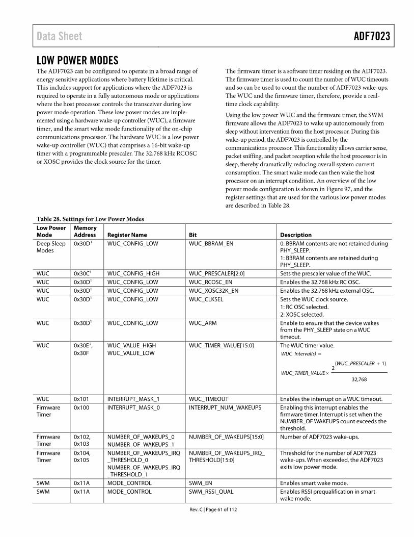
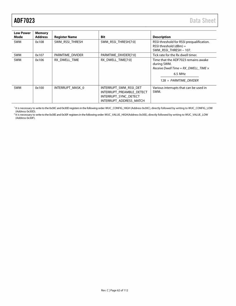
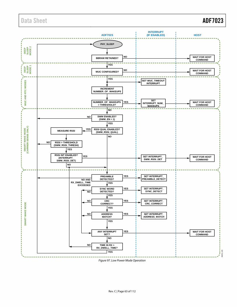
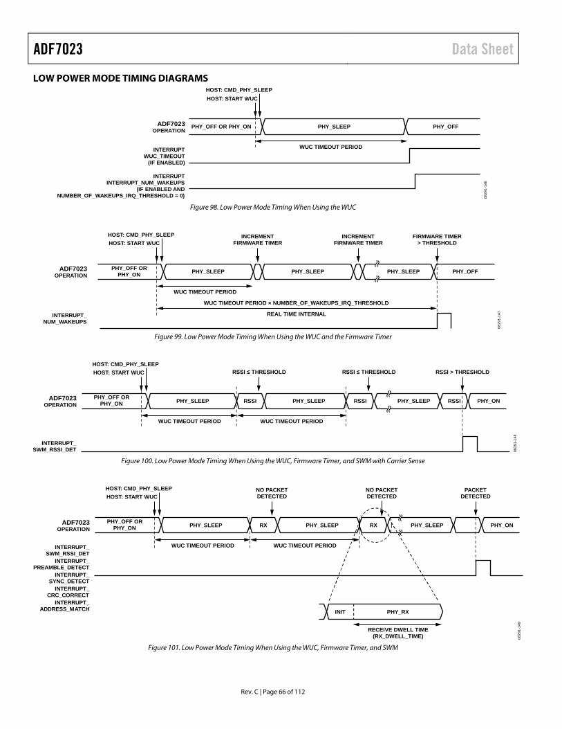
The smart wake mode (SWM) allows the ADF7023 to wake up autonomously from sleep using the internal wake-up timer without intervention from the host processor. After wake-up, the ADF7023 is controlled by the communications processor. This functionality allows carrier sense, packet sniffing, and packet reception while the host processor is in sleep, thereby reducing overall system current consumption. The smart wake mode can wake the host processor on an interrupt condition.
These interrupt conditions can be configured to include the reception of valid preamble, sync word, CRC, or address match. Wake-up from sleep mode can also be triggered by the host processor. For systems requiring very accurate wake-up timing, a 32 kHz oscillator can be used to drive the wake-up timer. Alternatively, the internal RC oscillator can be used, which gives lower current consumption in sleep.
The ADF7023 features an advanced encryption standard (AES) engine with hardware acceleration that provides 128-bit block encryption and decryption with key sizes of 128 bits, 192 bits, and 256 bits. Both electronic code book (ECB) and Cipher Block Chaining Mode 1 (CBC Mode 1) are supported. The AES engine can be used to encrypt/decrypt packet data and can be used as a standalone engine for encryption/decryption by the host processor. The AES engine is enabled on the ADF7023 by downloading the AES software module to program RAM. The AES software module is available from Analog Devices, Inc.
An on-chip, 8-bit ADC provides readback of an external analog input, the RSSI signal, or an integrated temperature sensor. An integrated battery voltage monitor raises an interrupt flag to the host processor whenever the battery voltage drops below a user-defined threshold.
ADF7023 Data Sheet
Rev. C | Page 6 of 112
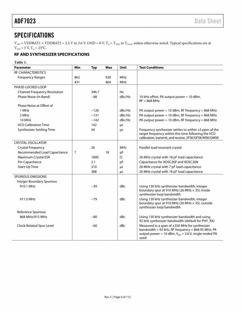
SPECIFICATIONS VDD = VDDBAT1 = VDDBAT2 = 2.2 V to 3.6 V, GND = 0 V, TA = TMIN to TMAX, unless otherwise noted. Typical specifications are at VDD = 3 V, TA = 25°C.
RF AND SYNTHESIZER SPECIFICATIONS
Table 1. Parameter Min Typ Max Unit Test Conditions RF CHARACTERISTICS
Frequency Ranges 862 928 MHz 431 464 MHz
PHASE-LOCKED LOOP Channel Frequency Resolution 396.7 Hz Phase Noise (In-Band) −88 dBc/Hz 10 kHz offset, PA output power = 10 dBm,
RF = 868 MHz Phase Noise at Offset of
1 MHz −126 dBc/Hz PA output power = 10 dBm, RF frequency = 868 MHz 2 MHz −131 dBc/Hz PA output power = 10 dBm, RF frequency = 868 MHz 10 MHz −142 dBc/Hz PA output power = 10 dBm, RF frequency = 868 MHz
VCO Calibration Time 142 µs Synthesizer Settling Time 56 µs Frequency synthesizer settles to within ±5 ppm of the
target frequency within this time following the VCO calibration, transmit, and receive, 2FSK/GFSK/MSK/GMSK
CRYSTAL OSCILLATOR Crystal Frequency 26 MHz Parallel load resonant crystal Recommended Load Capacitance 7 18 pF Maximum Crystal ESR 1800 Ω 26 MHz crystal with 18 pF load capacitance Pin Capacitance 2.1 pF Capacitance for XOSC26P and XOSC26N Start-Up Time 310 µs 26 MHz crystal with 7 pF load capacitance 388 µs 26 MHz crystal with 18 pF load capacitance
Reference Spurious 868 MHz/915 MHz −80 dBc Using 130 kHz synthesizer bandwidth and using
92 kHz synthesizer bandwidth (default for PHY_RX) Clock-Related Spur Level −60 dBc Measured in a span of ±350 MHz for synthesizer
bandwidth = 92 kHz, RF frequency = 868.95 MHz, PA output power = 10 dBm, VDD = 3.6 V, single-ended PA used
Data Sheet ADF7023
Rev. C | Page 7 of 112
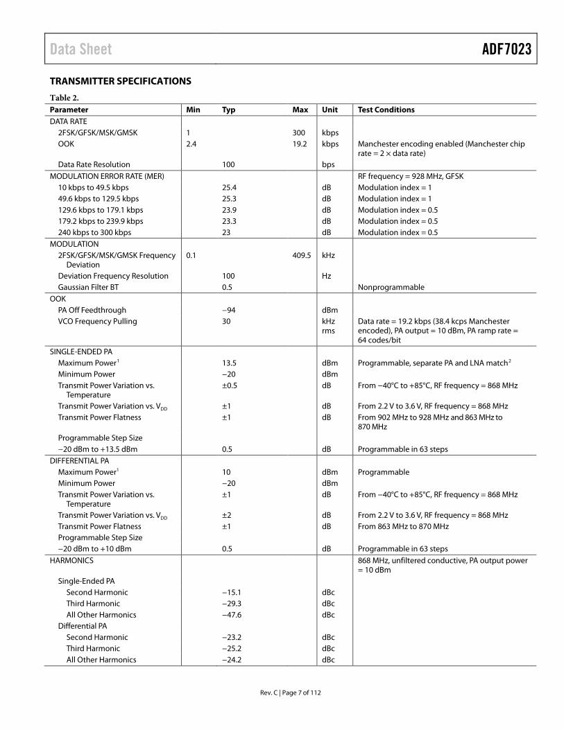
TRANSMITTER SPECIFICATIONS
Table 2. Parameter Min Typ Max Unit Test Conditions DATA RATE
2FSK/GFSK/MSK/GMSK 1 300 kbps OOK 2.4 19.2 kbps Manchester encoding enabled (Manchester chip
rate = 2 × data rate) Data Rate Resolution 100 bps
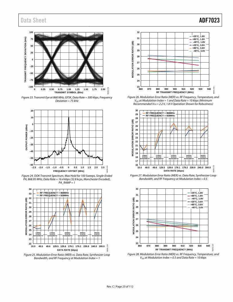
MODULATION ERROR RATE (MER) RF frequency = 928 MHz, GFSK 10 kbps to 49.5 kbps 25.4 dB Modulation index = 1 49.6 kbps to 129.5 kbps 25.3 dB Modulation index = 1 129.6 kbps to 179.1 kbps 23.9 dB Modulation index = 0.5 179.2 kbps to 239.9 kbps 23.3 dB Modulation index = 0.5 240 kbps to 300 kbps 23 dB Modulation index = 0.5
MODULATION 2FSK/GFSK/MSK/GMSK Frequency
Deviation
0.1 409.5 kHz
Deviation Frequency Resolution 100 Hz Gaussian Filter BT 0.5 Nonprogrammable
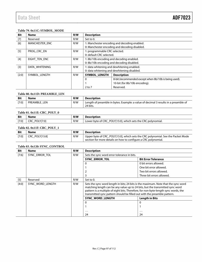
OOK PA Off Feedthrough −94 dBm VCO Frequency Pulling 30 kHz
rms Data rate = 19.2 kbps (38.4 kcps Manchester encoded), PA output = 10 dBm, PA ramp rate = 64 codes/bit
SINGLE-ENDED PA Maximum Power1
13.5 dBm Programmable, separate PA and LNA match2 Minimum Power −20 dBm Transmit Power Variation vs.
Temperature ±0.5 dB From −40°C to +85°C, RF frequency = 868 MHz
Transmit Power Variation vs. VDD ±1 dB From 2.2 V to 3.6 V, RF frequency = 868 MHz Transmit Power Flatness ±1 dB From 902 MHz to 928 MHz and 863 MHz to
870 MHz Programmable Step Size −20 dBm to +13.5 dBm 0.5 dB Programmable in 63 steps
DIFFERENTIAL PA Maximum Power1
10 dBm Programmable Minimum Power −20 dBm Transmit Power Variation vs.
Temperature ±1 dB From −40°C to +85°C, RF frequency = 868 MHz
Transmit Power Variation vs. VDD ±2 dB From 2.2 V to 3.6 V, RF frequency = 868 MHz Transmit Power Flatness ±1 dB From 863 MHz to 870 MHz Programmable Step Size −20 dBm to +10 dBm 0.5 dB Programmable in 63 steps
HARMONICS 868 MHz, unfiltered conductive, PA output power = 10 dBm
Single-Ended PA Second Harmonic −15.1 dBc Third Harmonic −29.3 dBc All Other Harmonics −47.6 dBc
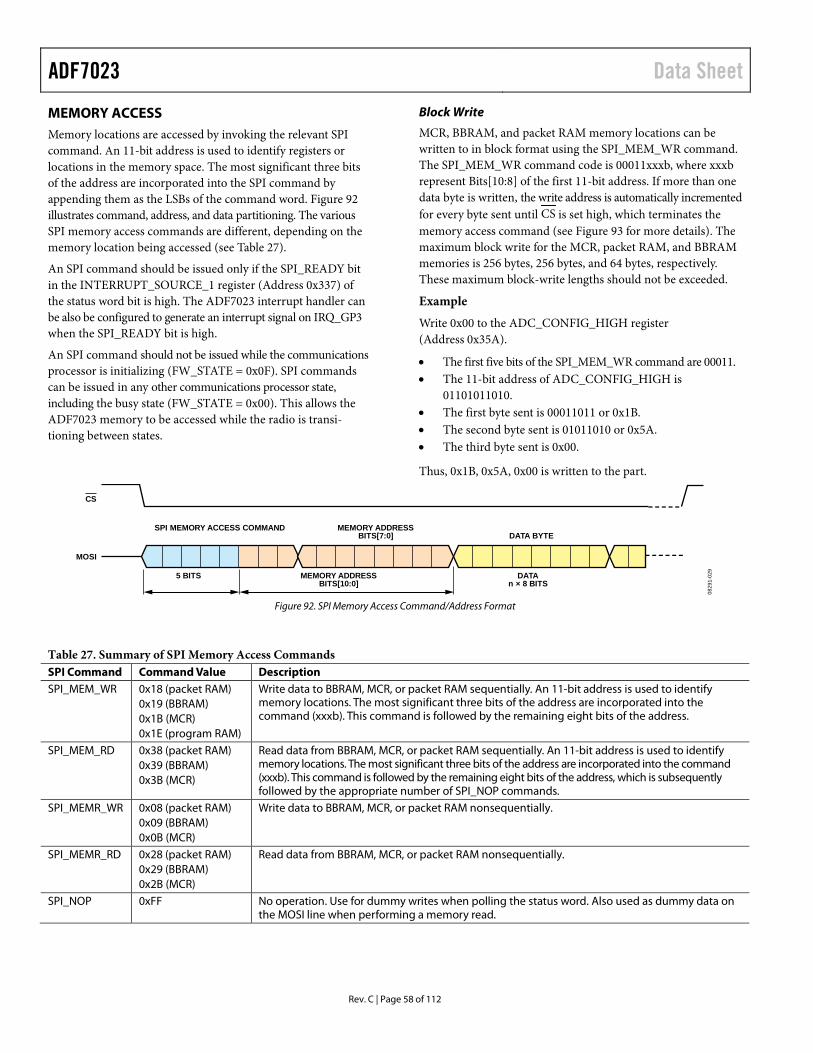
Differential PA Second Harmonic −23.2 dBc Third Harmonic −25.2 dBc All Other Harmonics −24.2 dBc
ADF7023 Data Sheet
Rev. C | Page 8 of 112
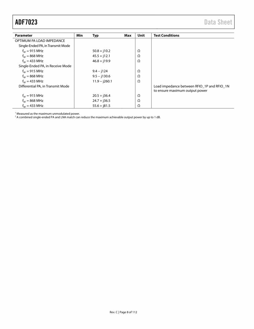
Parameter Min Typ Max Unit Test Conditions OPTIMUM PA LOAD IMPEDANCE
1 Measured as the maximum unmodulated power. 2 A combined single-ended PA and LNA match can reduce the maximum achievable output power by up to 1 dB.
Data Sheet ADF7023
Rev. C | Page 9 of 112
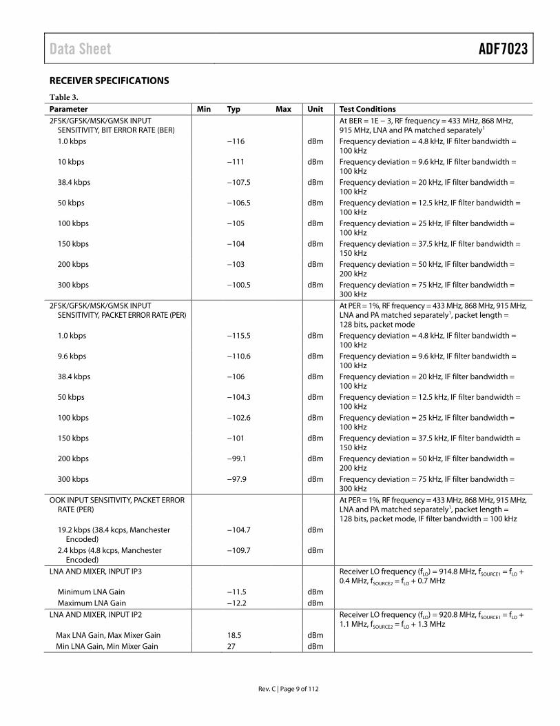
RECEIVER SPECIFICATIONS
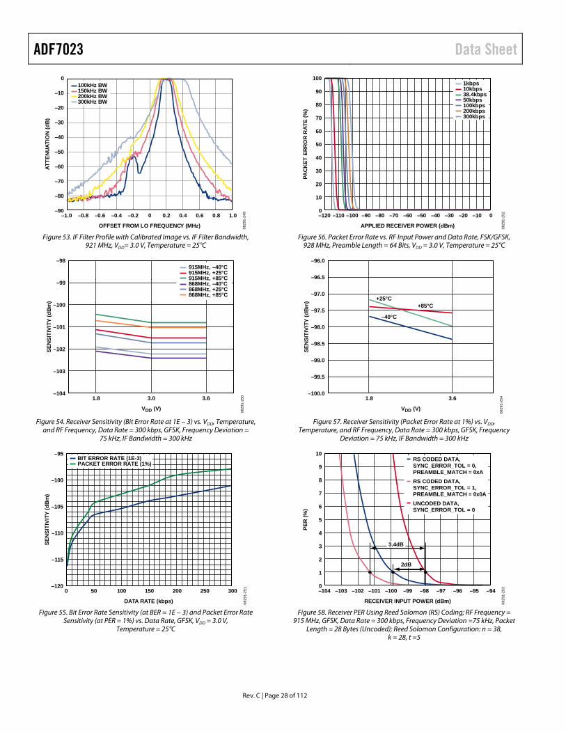
Table 3. Parameter Min Typ Max Unit Test Conditions 2FSK/GFSK/MSK/GMSK INPUT
SENSITIVITY, BIT ERROR RATE (BER) At BER = 1E − 3, RF frequency = 433 MHz, 868 MHz,
915 MHz, LNA and PA matched separately1 1.0 kbps −116 dBm Frequency deviation = 4.8 kHz, IF filter bandwidth =
100 kHz 10 kbps −111 dBm Frequency deviation = 9.6 kHz, IF filter bandwidth =
100 kHz 38.4 kbps −107.5 dBm Frequency deviation = 20 kHz, IF filter bandwidth =
100 kHz 50 kbps −106.5 dBm Frequency deviation = 12.5 kHz, IF filter bandwidth =
100 kHz 100 kbps −105 dBm Frequency deviation = 25 kHz, IF filter bandwidth =
100 kHz 150 kbps −104 dBm Frequency deviation = 37.5 kHz, IF filter bandwidth =
150 kHz 200 kbps −103 dBm Frequency deviation = 50 kHz, IF filter bandwidth =
200 kHz 300 kbps −100.5 dBm Frequency deviation = 75 kHz, IF filter bandwidth =
300 kHz 2FSK/GFSK/MSK/GMSK INPUT
SENSITIVITY, PACKET ERROR RATE (PER) At PER = 1%, RF frequency = 433 MHz, 868 MHz, 915 MHz,
LNA and PA matched separately1, packet length = 128 bits, packet mode
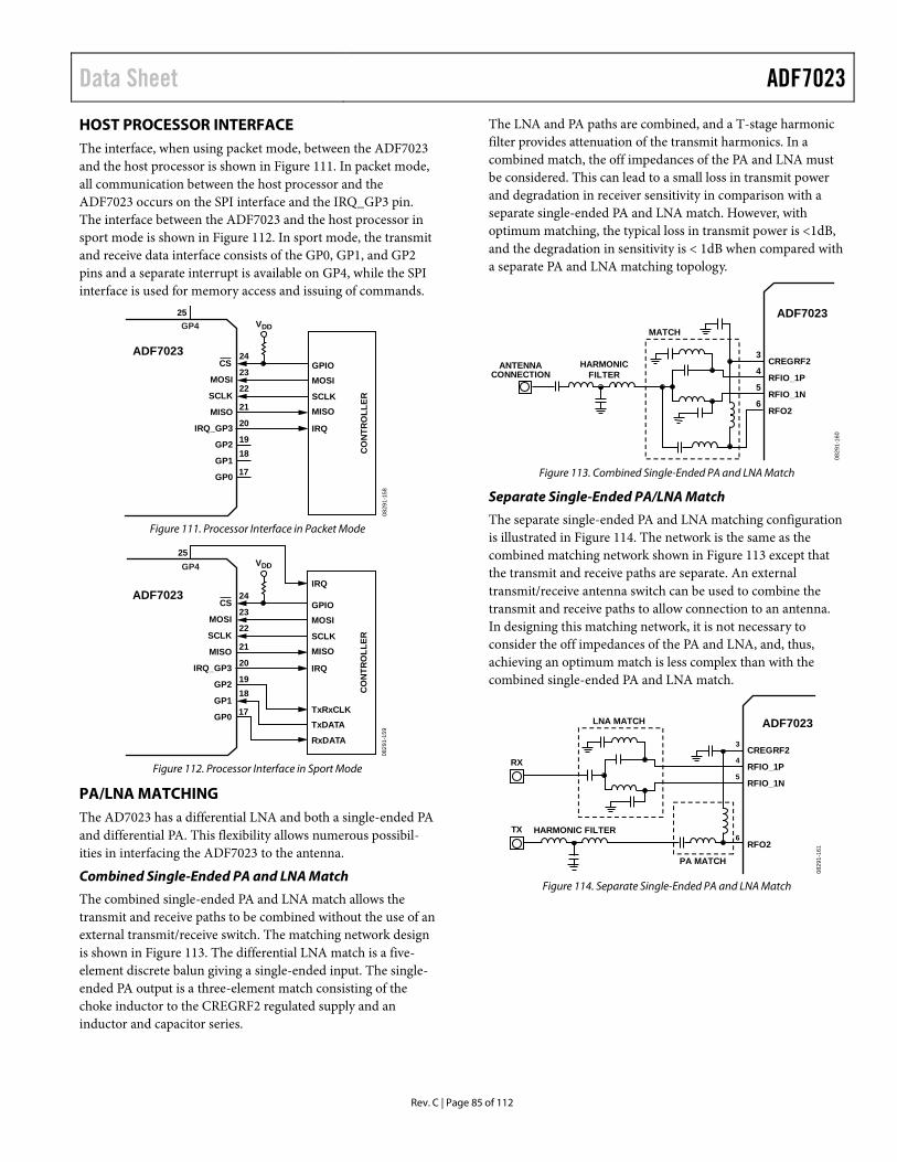
1.0 kbps −115.5 dBm Frequency deviation = 4.8 kHz, IF filter bandwidth = 100 kHz
9.6 kbps −110.6 dBm Frequency deviation = 9.6 kHz, IF filter bandwidth = 100 kHz
38.4 kbps −106 dBm Frequency deviation = 20 kHz, IF filter bandwidth = 100 kHz
50 kbps −104.3 dBm Frequency deviation = 12.5 kHz, IF filter bandwidth = 100 kHz
100 kbps −102.6 dBm Frequency deviation = 25 kHz, IF filter bandwidth = 100 kHz
150 kbps −101 dBm Frequency deviation = 37.5 kHz, IF filter bandwidth = 150 kHz
200 kbps −99.1 dBm Frequency deviation = 50 kHz, IF filter bandwidth = 200 kHz
300 kbps −97.9 dBm Frequency deviation = 75 kHz, IF filter bandwidth = 300 kHz
OOK INPUT SENSITIVITY, PACKET ERROR RATE (PER)
At PER = 1%, RF frequency = 433 MHz, 868 MHz, 915 MHz, LNA and PA matched separately1, packet length = 128 bits, packet mode, IF filter bandwidth = 100 kHz
19.2 kbps (38.4 kcps, Manchester Encoded)
−104.7 dBm
2.4 kbps (4.8 kcps, Manchester Encoded)
−109.7 dBm
LNA AND MIXER, INPUT IP3 Receiver LO frequency (fLO) = 914.8 MHz, fSOURCE1 = fLO + 0.4 MHz, fSOURCE2 = fLO + 0.7 MHz
Minimum LNA Gain −11.5 dBm Maximum LNA Gain −12.2 dBm
LNA AND MIXER, INPUT IP2 Receiver LO frequency (fLO) = 920.8 MHz, fSOURCE1 = fLO + 1.1 MHz, fSOURCE2 = fLO + 1.3 MHz
Max LNA Gain, Max Mixer Gain 18.5 dBm Min LNA Gain, Min Mixer Gain 27 dBm
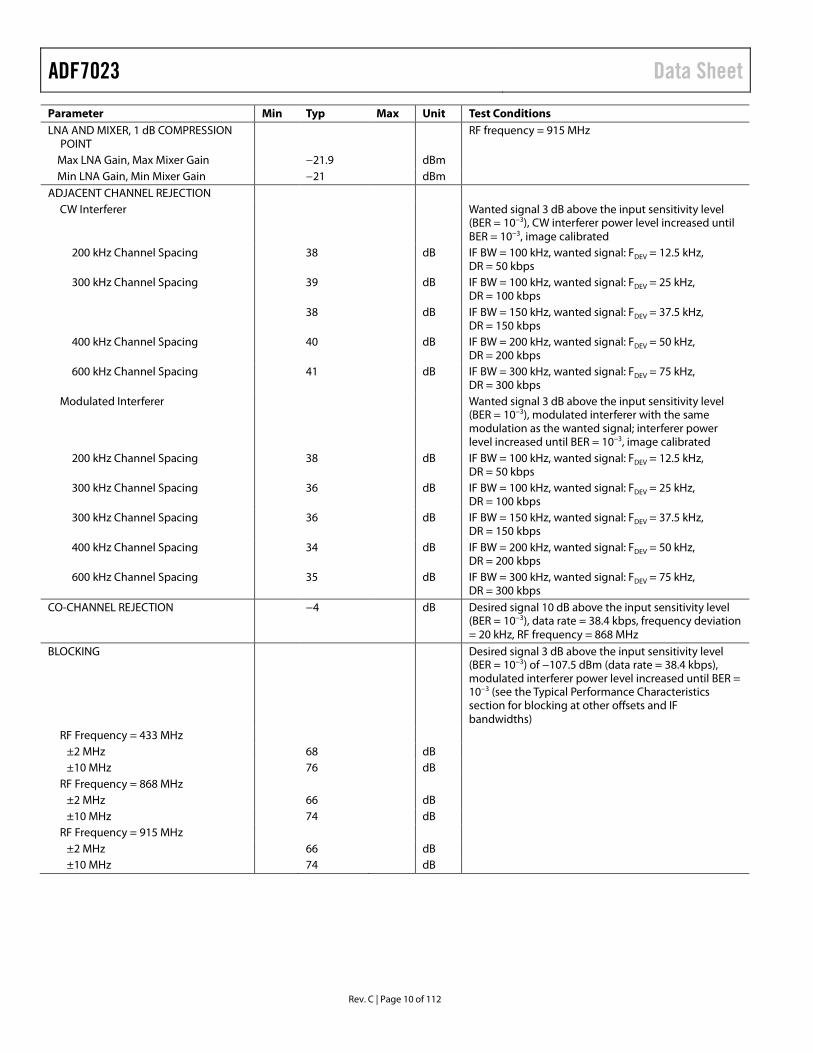
ADF7023 Data Sheet
Rev. C | Page 10 of 112
Parameter Min Typ Max Unit Test Conditions LNA AND MIXER, 1 dB COMPRESSION
POINT RF frequency = 915 MHz
Max LNA Gain, Max Mixer Gain −21.9 dBm Min LNA Gain, Min Mixer Gain −21 dBm
ADJACENT CHANNEL REJECTION CW Interferer Wanted signal 3 dB above the input sensitivity level
(BER = 10−3), CW interferer power level increased until BER = 10−3, image calibrated
200 kHz Channel Spacing 38 dB IF BW = 100 kHz, wanted signal: FDEV = 12.5 kHz, DR = 50 kbps
300 kHz Channel Spacing 39 dB IF BW = 100 kHz, wanted signal: FDEV = 25 kHz, DR = 100 kbps
38 dB IF BW = 150 kHz, wanted signal: FDEV = 37.5 kHz, DR = 150 kbps
400 kHz Channel Spacing 40 dB IF BW = 200 kHz, wanted signal: FDEV = 50 kHz, DR = 200 kbps
600 kHz Channel Spacing 41 dB IF BW = 300 kHz, wanted signal: FDEV = 75 kHz, DR = 300 kbps
Modulated Interferer Wanted signal 3 dB above the input sensitivity level (BER = 10−3), modulated interferer with the same modulation as the wanted signal; interferer power level increased until BER = 10−3, image calibrated
200 kHz Channel Spacing 38 dB IF BW = 100 kHz, wanted signal: FDEV = 12.5 kHz, DR = 50 kbps
300 kHz Channel Spacing 36 dB IF BW = 100 kHz, wanted signal: FDEV = 25 kHz, DR = 100 kbps
300 kHz Channel Spacing 36 dB IF BW = 150 kHz, wanted signal: FDEV = 37.5 kHz, DR = 150 kbps
400 kHz Channel Spacing 34 dB IF BW = 200 kHz, wanted signal: FDEV = 50 kHz, DR = 200 kbps
600 kHz Channel Spacing 35 dB IF BW = 300 kHz, wanted signal: FDEV = 75 kHz, DR = 300 kbps
CO-CHANNEL REJECTION −4 dB Desired signal 10 dB above the input sensitivity level (BER = 10−3), data rate = 38.4 kbps, frequency deviation = 20 kHz, RF frequency = 868 MHz
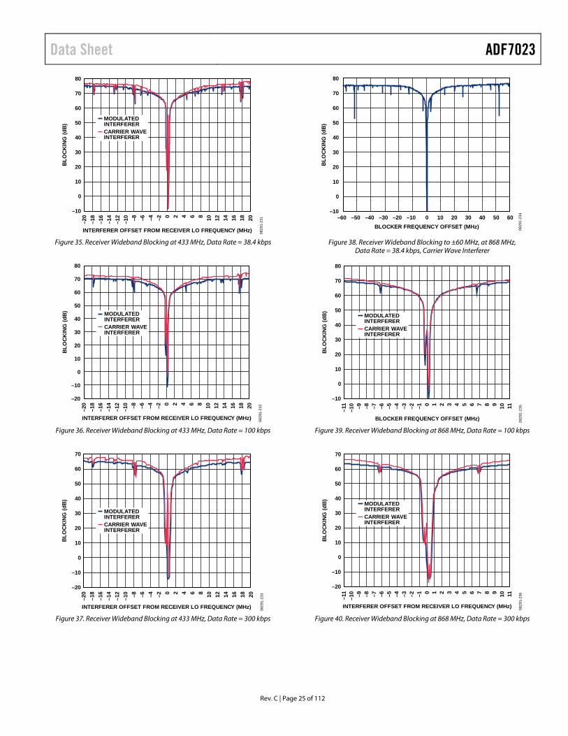
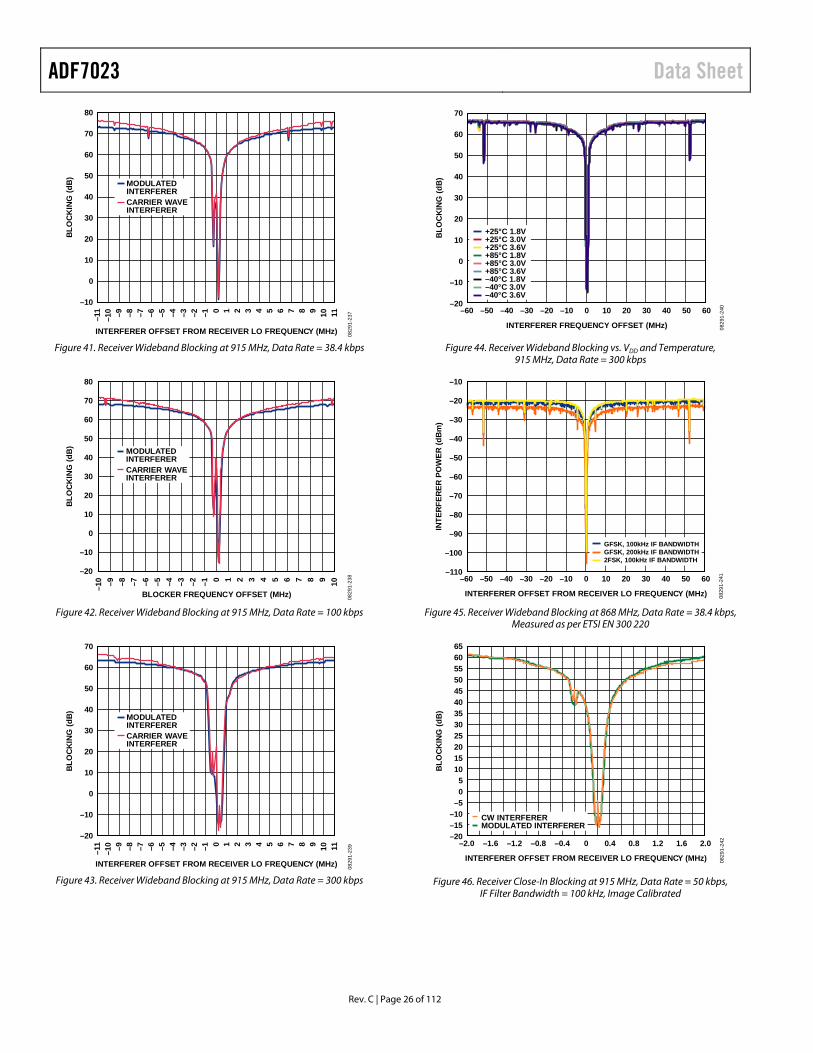
BLOCKING Desired signal 3 dB above the input sensitivity level (BER = 10−3) of −107.5 dBm (data rate = 38.4 kbps), modulated interferer power level increased until BER = 10−3 (see the Typical Performance Characteristics section for blocking at other offsets and IF bandwidths)
RF Frequency = 433 MHz ±2 MHz 68 dB ±10 MHz 76 dB
RF Frequency = 868 MHz ±2 MHz 66 dB ±10 MHz 74 dB
RF Frequency = 915 MHz ±2 MHz 66 dB ±10 MHz 74 dB
Data Sheet ADF7023
Rev. C | Page 11 of 112
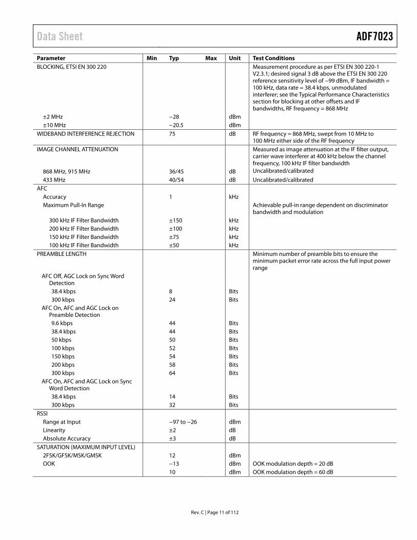
Parameter Min Typ Max Unit Test Conditions BLOCKING, ETSI EN 300 220 Measurement procedure as per ETSI EN 300 220-1
V2.3.1; desired signal 3 dB above the ETSI EN 300 220 reference sensitivity level of −99 dBm, IF bandwidth = 100 kHz, data rate = 38.4 kbps, unmodulated interferer; see the Typical Performance Characteristics section for blocking at other offsets and IF bandwidths, RF frequency = 868 MHz
±2 MHz −28 dBm ±10 MHz −20.5 dBm
WIDEBAND INTERFERENCE REJECTION 75 dB RF frequency = 868 MHz, swept from 10 MHz to 100 MHz either side of the RF frequency
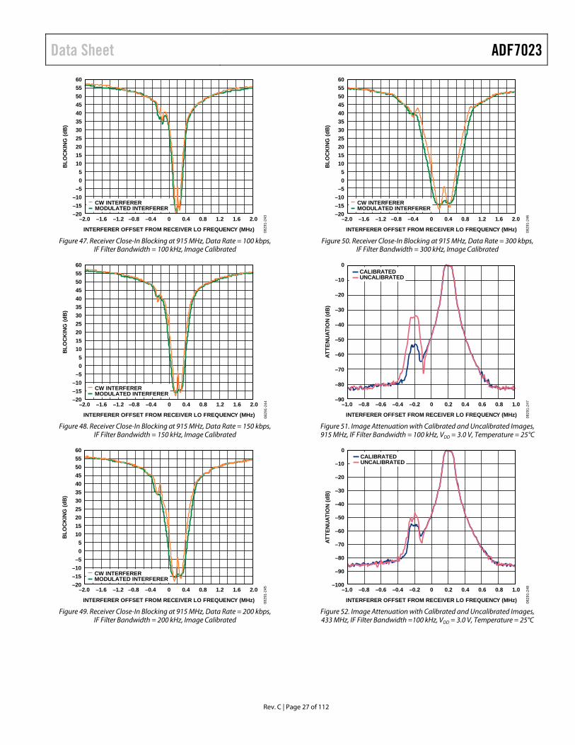
IMAGE CHANNEL ATTENUATION Measured as image attenuation at the IF filter output, carrier wave interferer at 400 kHz below the channel frequency, 100 kHz IF filter bandwidth
868 MHz, 915 MHz 36/45 dB Uncalibrated/calibrated
433 MHz 40/54 dB Uncalibrated/calibrated AFC
Accuracy 1 kHz Maximum Pull-In Range Achievable pull-in range dependent on discriminator
bandwidth and modulation 300 kHz IF Filter Bandwidth ±150 kHz 200 kHz IF Filter Bandwidth ±100 kHz 150 kHz IF Filter Bandwidth ±75 kHz 100 kHz IF Filter Bandwidth ±50 kHz
PREAMBLE LENGTH Minimum number of preamble bits to ensure the minimum packet error rate across the full input power range
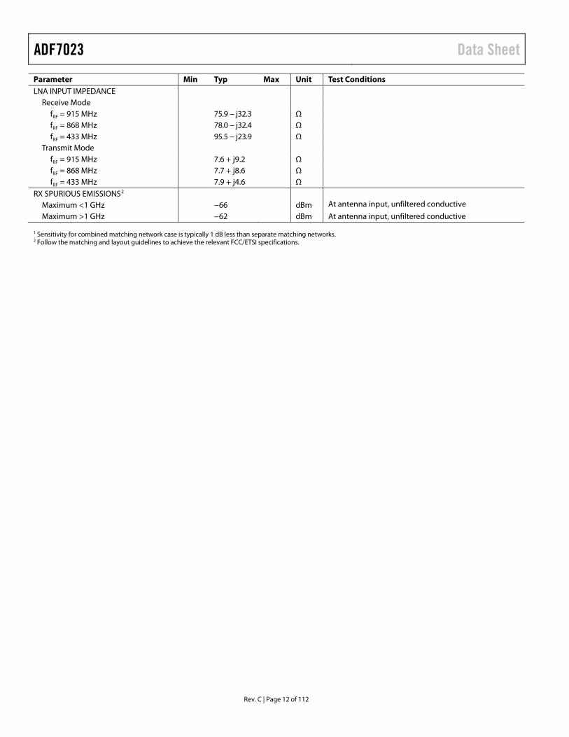
Maximum <1 GHz −66 dBm At antenna input, unfiltered conductive
Maximum >1 GHz −62 dBm At antenna input, unfiltered conductive 1 Sensitivity for combined matching network case is typically 1 dB less than separate matching networks. 2 Follow the matching and layout guidelines to achieve the relevant FCC/ETSI specifications.
ADF7023
Rev. C | Page 13 of 112
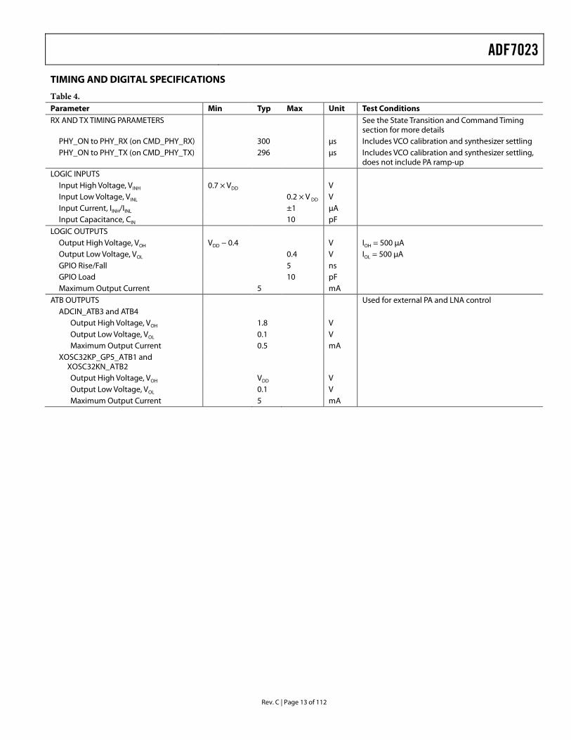
TIMING AND DIGITAL SPECIFICATIONS
Table 4. Parameter Min Typ Max Unit Test Conditions RX AND TX TIMING PARAMETERS See the State Transition and Command Timing
section for more details PHY_ON to PHY_RX (on CMD_PHY_RX) 300 μs Includes VCO calibration and synthesizer settling PHY_ON to PHY_TX (on CMD_PHY_TX) 296 μs Includes VCO calibration and synthesizer settling,
does not include PA ramp-up LOGIC INPUTS
Input High Voltage, VINH 0.7 × VDD V Input Low Voltage, VINL 0.2 × V DD V Input Current, IINH/IINL ±1 µA Input Capacitance, CIN 10 pF
LOGIC OUTPUTS Output High Voltage, VOH VDD − 0.4 V IOH = 500 µA Output Low Voltage, VOL 0.4 V IOL = 500 µA GPIO Rise/Fall 5 ns GPIO Load 10 pF Maximum Output Current 5 mA
ATB OUTPUTS Used for external PA and LNA control ADCIN_ATB3 and ATB4
Output High Voltage, VOH 1.8 V Output Low Voltage, VOL 0.1 V Maximum Output Current 0.5 mA
XOSC32KP_GP5_ATB1 and XOSC32KN_ATB2
Output High Voltage, VOH VDD V Output Low Voltage, VOL 0.1 V Maximum Output Current 5 mA
ADF7023 Data Sheet
Rev. C | Page 14 of 112
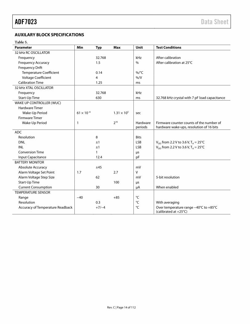
AUXILARY BLOCK SPECIFICATIONS
Table 5. Parameter Min Typ Max Unit Test Conditions 32 kHz RC OSCILLATOR
Frequency 32.768 kHz After calibration Frequency Accuracy 1.5 % After calibration at 25°C Frequency Drift
Temperature Coefficient 0.14 %/°C Voltage Coefficient 4 %/V
Calibration Time 1.25 ms 32 kHz XTAL OSCILLATOR
Frequency 32.768 kHz Start-Up Time 630 ms 32.768 kHz crystal with 7 pF load capacitance
Firmware counter counts of the number of hardware wake-ups, resolution of 16 bits
ADC Resolution 8 Bits DNL ±1 LSB VDD from 2.2 V to 3.6 V, TA = 25°C INL ±1 LSB VDD from 2.2 V to 3.6 V, TA = 25°C Conversion Time 1 µs Input Capacitance 12.4 pF
BATTERY MONITOR Absolute Accuracy ±45 mV
Alarm Voltage Set Point 1.7 2.7 V Alarm Voltage Step Size 62 mV 5-bit resolution Start-Up Time 100 µs Current Consumption 30 µA When enabled
TEMPERATURE SENSOR Range −40 +85 °C Resolution 0.3 °C With averaging Accuracy of Temperature Readback +7/−4 °C Over temperature range −40°C to +85°C
(calibrated at +25°C)
Data Sheet ADF7023
Rev. C | Page 15 of 112
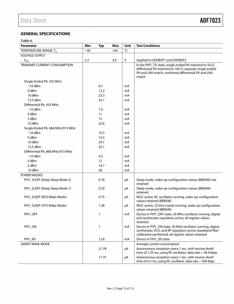
GENERAL SPECIFICATIONS
Table 6. Parameter Min Typ Max Unit Test Conditions TEMPERATURE RANGE, TA −40 +85 °C VOLTAGE SUPPLY
VDD 2.2 3.6 V Applied to VDDBAT1 and VDDBAT2 TRANSMIT CURRENT CONSUMPTION In the PHY_TX state, single-ended PA matched to 50 Ω,
differential PA matched to 100 Ω, separate single-ended PA and LNA match, combined differential PA and LNA match
Single-Ended PA, 433 MHz −10 dBm 8.7 mA 0 dBm 12.2 mA 10 dBm 23.3 mA 13.5 dBm 32.1 mA
Differential PA, 433 MHz −10 dBm 7.9 mA 0 dBm 11 mA 5 dBm 15 mA 10 dBm 22.6 mA
Single-Ended PA, 868 MHz/915 MHz −10 dBm 10.3 mA 0 dBm 13.3 mA 10 dBm 24.1 mA 13.5 dBm 32.1 mA
Differential PA, 868 MHz/915 MHz −10 dBm 9.3 mA 0 dBm 12 mA 5 dBm 16.7 mA 10 dBm 28 mA
POWER MODES PHY_SLEEP (Deep Sleep Mode 2) 0.18 µA Sleep mode, wake-up configuration values (BBRAM) not
values retained (BBRAM) PHY_OFF 1 mA Device in PHY_OFF state, 26 MHz oscillator running, digital
and synthesizer regulators active, all register values retained
PHY_ON 1 mA Device in PHY_ON state, 26 MHz oscillator running, digital, synthesizer, VCO, and RF regulators active, baseband filter calibration performed, all register values retained
PHY_RX 12.8 mA Device in PHY_RX state SMART WAKE MODE Average current consumption
21.78 µA Autonomous reception every 1 sec, with receive dwell time of 1.25 ms, using RC oscillator, data rate = 38.4 kbps
11.75 µA Autonomous reception every 1 sec, with receive dwell time of 0.5 ms, using RC oscillator, data rate = 300 kbps
ADF7023 Data Sheet
Rev. C | Page 16 of 112
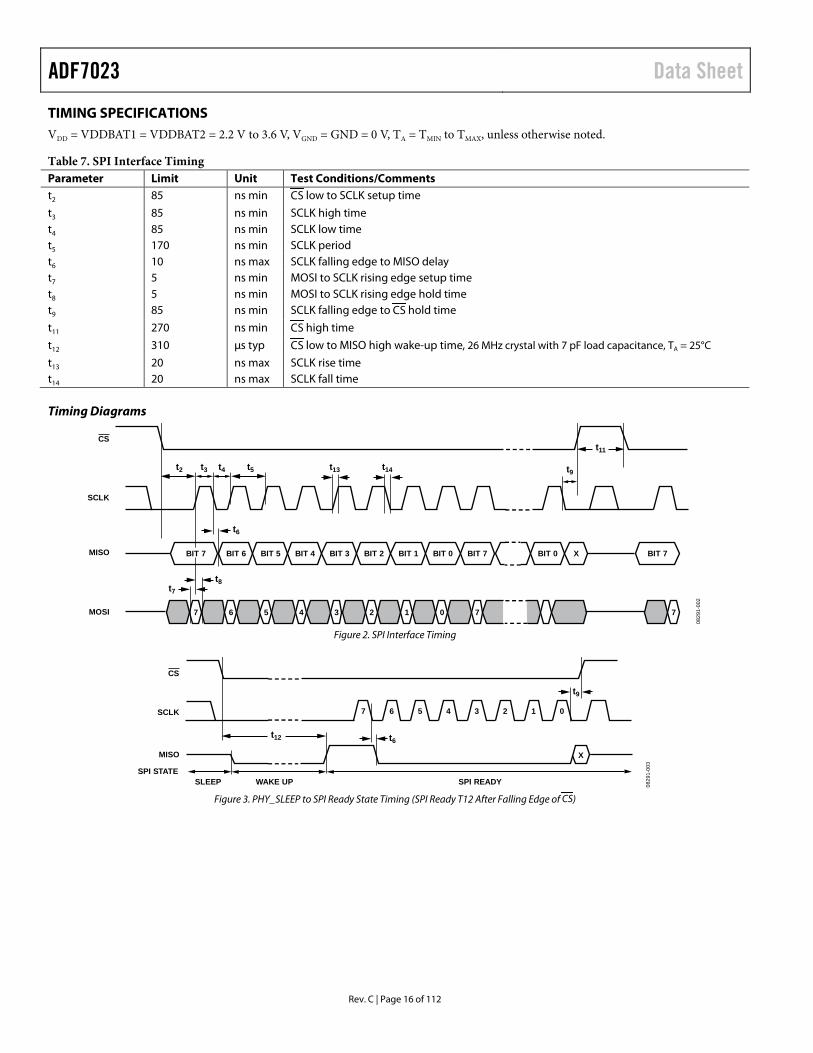
TIMING SPECIFICATIONS VDD = VDDBAT1 = VDDBAT2 = 2.2 V to 3.6 V, VGND = GND = 0 V, TA = TMIN to TMAX, unless otherwise noted.
Table 7. SPI Interface Timing Parameter Limit Unit Test Conditions/Comments t2 85 ns min CS low to SCLK setup time
t3 85 ns min SCLK high time t4 85 ns min SCLK low time t5 170 ns min SCLK period t6 10 ns max SCLK falling edge to MISO delay t7 5 ns min MOSI to SCLK rising edge setup time t8 5 ns min MOSI to SCLK rising edge hold time t9 85 ns min SCLK falling edge to CS hold time
t11 270 ns min CS high time
t12 310 µs typ CS low to MISO high wake-up time, 26 MHz crystal with 7 pF load capacitance, TA = 25°C
t13 20 ns max SCLK rise time t14 20 ns max SCLK fall time
Timing Diagrams
Figure 2. SPI Interface Timing
Figure 3. PHY_SLEEP to SPI Ready State Timing (SPI Ready T12 After Falling Edge of CS)
t11
t9t4 t5 t13t3t2 t14
t6
t8t7
CS
SCLK
MISO
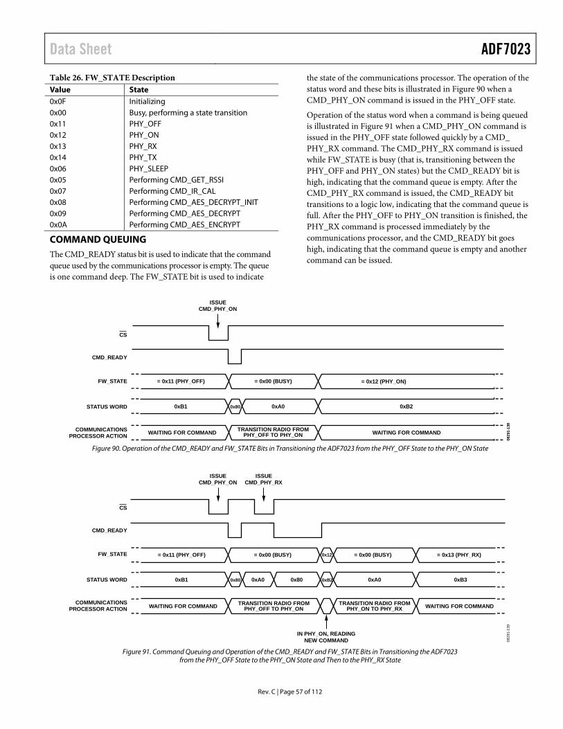
MOSI 7 76 5 4 3 2 1 0 7
BIT 7 BIT 6 BIT 5 BIT 4 BIT 3 BIT 2 BIT 1 BIT 0 BIT 7 BIT 0 X BIT 7
0829
1-00
2
SPI STATE
CS
SCLK
MISO
SLEEP WAKE UP SPI READY
X
012345
t9
67
t6t12
0829
1-00
3
Data Sheet ADF7023
Rev. C | Page 17 of 112
ABSOLUTE MAXIMUM RATINGS TA = 25°C, unless otherwise noted.
Table 8. Parameter Rating VDDBAT1, VDDBAT2 to GND −0.3 V to +3.96 V Operating Temperature Range
Industrial −40°C to +85°C Storage Temperature Range −65°C to +125°C Maximum Junction Temperature 150°C LFCSP θJA Thermal Impedance 26°C/W Reflow Soldering
Peak Temperature 260°C Time at Peak Temperature 40 sec
Stresses above those listed under Absolute Maximum Ratings may cause permanent damage to the device. This is a stress rating only; functional operation of the device at these or any other conditions above those indicated in the operational section of this specification is not implied. Exposure to absolute maximum rating conditions for extended periods may affect device reliability.
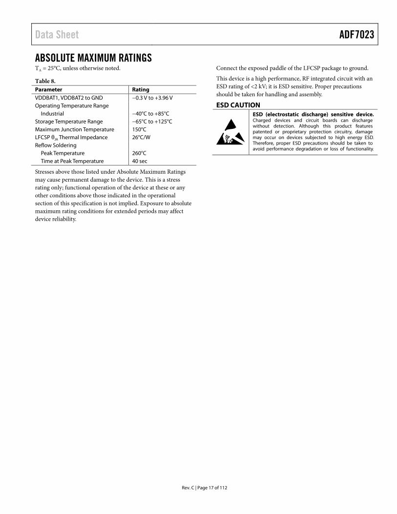
Connect the exposed paddle of the LFCSP package to ground.
This device is a high performance, RF integrated circuit with an ESD rating of <2 kV; it is ESD sensitive. Proper precautions should be taken for handling and assembly.
ESD CAUTION
ADF7023 Data Sheet
Rev. C | Page 18 of 112
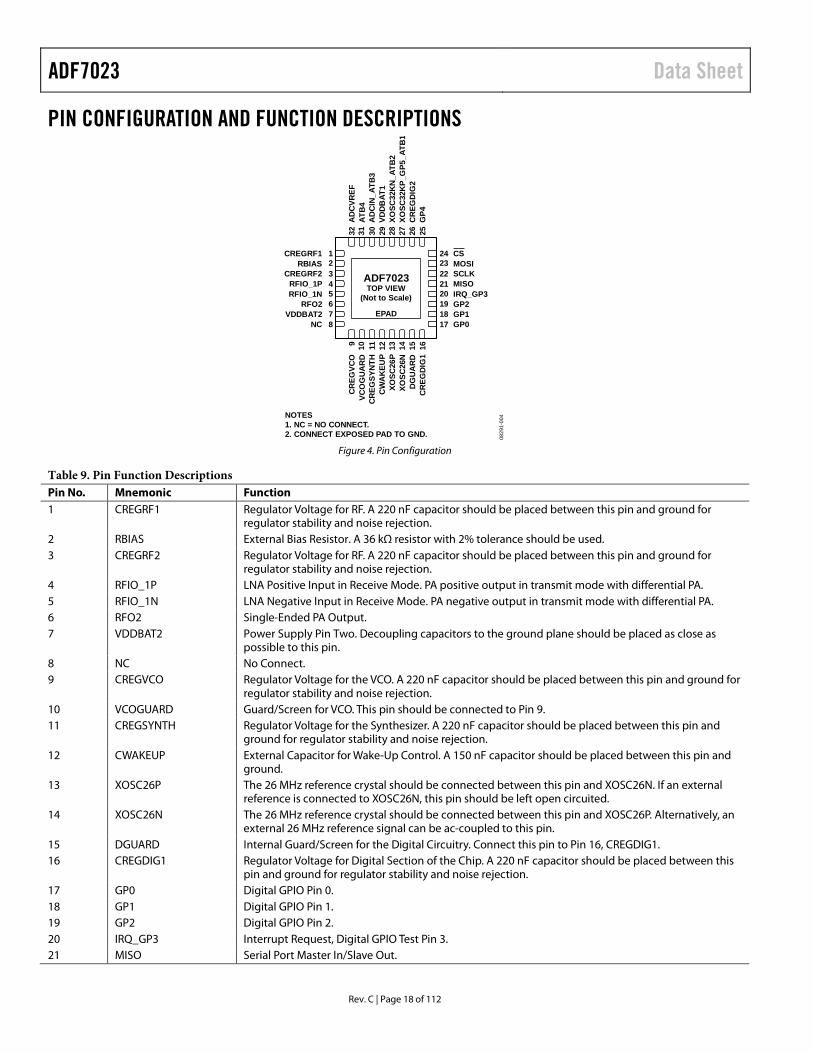
PIN CONFIGURATION AND FUNCTION DESCRIPTIONS
Figure 4. Pin Configuration
Table 9. Pin Function Descriptions Pin No. Mnemonic Function 1 CREGRF1 Regulator Voltage for RF. A 220 nF capacitor should be placed between this pin and ground for
regulator stability and noise rejection. 2 RBIAS External Bias Resistor. A 36 kΩ resistor with 2% tolerance should be used. 3 CREGRF2 Regulator Voltage for RF. A 220 nF capacitor should be placed between this pin and ground for
regulator stability and noise rejection. 4 RFIO_1P LNA Positive Input in Receive Mode. PA positive output in transmit mode with differential PA. 5 RFIO_1N LNA Negative Input in Receive Mode. PA negative output in transmit mode with differential PA. 6 RFO2 Single-Ended PA Output. 7 VDDBAT2 Power Supply Pin Two. Decoupling capacitors to the ground plane should be placed as close as
possible to this pin. 8 NC No Connect. 9 CREGVCO Regulator Voltage for the VCO. A 220 nF capacitor should be placed between this pin and ground for
regulator stability and noise rejection. 10 VCOGUARD Guard/Screen for VCO. This pin should be connected to Pin 9. 11 CREGSYNTH Regulator Voltage for the Synthesizer. A 220 nF capacitor should be placed between this pin and
ground for regulator stability and noise rejection. 12 CWAKEUP External Capacitor for Wake-Up Control. A 150 nF capacitor should be placed between this pin and
ground. 13 XOSC26P The 26 MHz reference crystal should be connected between this pin and XOSC26N. If an external
reference is connected to XOSC26N, this pin should be left open circuited. 14 XOSC26N The 26 MHz reference crystal should be connected between this pin and XOSC26P. Alternatively, an
external 26 MHz reference signal can be ac-coupled to this pin. 15 DGUARD Internal Guard/Screen for the Digital Circuitry. Connect this pin to Pin 16, CREGDIG1. 16 CREGDIG1 Regulator Voltage for Digital Section of the Chip. A 220 nF capacitor should be placed between this
pin and ground for regulator stability and noise rejection. 17 GP0 Digital GPIO Pin 0. 18 GP1 Digital GPIO Pin 1. 19 GP2 Digital GPIO Pin 2. 20 IRQ_GP3 Interrupt Request, Digital GPIO Test Pin 3. 21 MISO Serial Port Master In/Slave Out.
NOTES1. NC = NO CONNECT.2. CONNECT EXPOSED PAD TO GND.
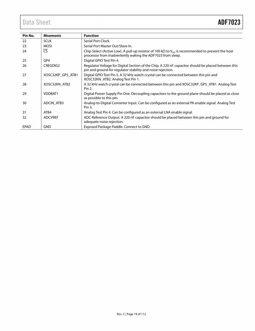
Pin No. Mnemonic Function 22 SCLK Serial Port Clock. 23 MOSI Serial Port Master Out/Slave In. 24 CS Chip Select (Active Low). A pull-up resistor of 100 kΩ to VDD is recommended to prevent the host
processor from inadvertently waking the ADF7023 from sleep. 25 GP4 Digital GPIO Test Pin 4. 26 CREGDIG2 Regulator Voltage for Digital Section of the Chip. A 220 nF capacitor should be placed between this
pin and ground for regulator stability and noise rejection. 27 XOSC32KP_GP5_ATB1 Digital GPIO Test Pin 5. A 32 kHz watch crystal can be connected between this pin and
XOSC32KN_ATB2. Analog Test Pin 1. 28 XOSC32KN_ATB2 A 32 kHz watch crystal can be connected between this pin and XOSC32KP_GP5_ATB1. Analog Test
Pin 2. 29 VDDBAT1 Digital Power Supply Pin One. Decoupling capacitors to the ground plane should be placed as close
as possible to this pin. 30 ADCIN_ATB3 Analog-to-Digital Converter Input. Can be configured as an external PA enable signal. Analog Test
Pin 3. 31 ATB4 Analog Test Pin 4. Can be configured as an external LNA enable signal. 32 ADCVREF ADC Reference Output. A 220 nF capacitor should be placed between this pin and ground for
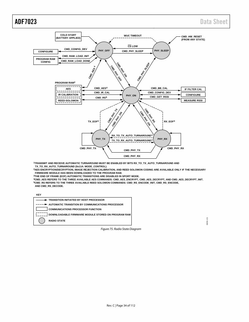
RADIO CONTROL The ADF7023 has five radio states designated PHY_SLEEP, PHY_OFF, PHY_ON, PHY_RX, and PHY_TX. The host processor can transition the ADF7023 between states by issuing single byte commands over the SPI interface. The various commands and states are illustrated in Figure 75. The communications processor handles the sequencing of various radio circuits and critical timing functions, thereby simplifying radio operation and easing the burden on the host processor.
RADIO STATES PHY_SLEEP
In this state, the device is in a low power sleep mode. To enter the state, issue the CMD_PHY_SLEEP command, either from the PHY_OFF or PHY_ON state. To wake the radio from the state, set the CS pin low, or use the wake-up controller (32.768 kHz RC or 32.768 kHz crystal) to wake the radio from this state. The wake-up timer should be set up before entering the PHY_SLEEP state. If retention of BBRAM contents is not required, Deep Sleep Mode 2 can be used to further reduce the PHY_SLEEP state current consumption. Deep Sleep Mode 2 is entered by issuing the CMD_HW_RESET command. The options for the PHY_SLEEP state are detailed in Table 10. When in PHY_SLEEP, the IRQ_GP3 interrupt pin is held at logic low while the other GPx pins are in a high impedance state.
PHY_OFF
In the PHY_OFF state, the 26 MHz crystal, the digital regulator, and the synthesizer regulator are powered up. All memories are fully accessible. The BBRAM registers must be valid before exiting this state.
PHY_ON
In the PHY_ON state, along with the crystal, the digital regulator and the synthesizer regulator, VCO, and RF regulators are powered up. A baseband filter calibration is performed when this state is entered from the PHY_OFF state if the BB_CAL bit in the MODE_CONTROL register (Address 0x11A) is set. The device is ready to operate, and the PHY_TX and PHY_RX states can be entered.
PHY_TX
In the PHY_TX state, the synthesizer is enabled and calibrated. The power amplifier is enabled, and the device transmits at the channel frequency defined by the CHANNEL_FREQ[23:0] setting (Address 0x109 to Address 0x10B). The state is entered by issuing
the CMD_PHY_TX command. The device automatically transmits the transmit packet stored in the packet RAM. After transmission of the packet, the PA is disabled and the device automatically returns to the PHY_ON state and can, optionally, generate an interrupt.
In sport mode, the device transmits the data present on the GP2 pin as described in the Sport section. The host processor must issue the CMD_PHY_ON command to exit the PHY_TX state when in sport mode.
PHY_RX
In the PHY_RX state, the synthesizer is enabled and calibrated. The ADC, RSSI, IF filter, mixer, and LNA are enabled. The radio is in receive mode on the channel frequency defined by the CHANNEL_FREQ[23:0] setting (Address 0x109 to Address 0x10B).
After reception of a valid packet, the device returns to the PHY_ON state and can, optionally, generate an interrupt. In sport mode, the device remains in the PHY_RX state until the CMD_PHY_ON command is issued.
Current Consumption
The typical current consumption in each state is detailed in Table 10.
Table 10. Current Consumption in ADF7023 Radio States
State Current (Typical) Conditions
PHY_SLEEP (Deep Sleep Mode 2)
0.18 µA Wake-up timer off, BBRAM contents not retained, entered by issuing CMD_HW_RESET
0.75 µA Wake-up timer on using a 32 kHz RC oscillator, BBRAM contents retained
PHY_SLEEP (XTO Mode )
1.28 µA Wake-up timer on using a 32 kHz XTAL oscillator, BBRAM contents retained
PHY_OFF 1.0 mA PHY_ON 1.0 mA PHY_TX 24.1 mA 10 dBm, single-ended PA, 868 MHz PHY_RX 12.8 mA
ADF7023 Data Sheet
Rev. C | Page 34 of 112
Figure 75. Radio State Diagram
CONFIGURE
PROGRAM RAMCONFIG
AES
IR CALIBRATION
REED-SOLOMON
IF FILTER CAL
CONFIGURE
MEASURE RSSI
RX_TO_TX_AUTO_TURNAROUND1
TX_TO_RX_AUTO_TURNAROUND1
CMD_PHY_TX
CMD_
PHY_
TX
CMD_PHY_RX
CMD_
PHY_
SLEE
P
CMD_
PHY_
ON
CMD_PHY_ON
CMD_PHY_ON
CMD_PHY_OFF
CMD_PHY_RX
COLD START(BATTERY APPLIED)
CMD_CONFIG_DEV
CMD_RAM_LOAD_INIT
CMD_RAM_LOAD_DONE
CMD_
AES
CMD_IR_CAL
CMD_AES4
CS LOW
WUC TIMEOUT
CMD_PHY_SLEEP
CMD_HW_RESET(FROM ANY STATE)
PHY_ON
PHY_TX PHY_RX
CMD_PHY_RXCMD_PHY_TX
TX_EOF3 RX_EOF3
PHY_OFF PHY_SLEEP
CMD_RS5
CMD_CONFIG_DEV
CMD_BB_CAL
CMD_GET_RSSI
PROGRAM RAM2
0829
1-12
1
1TRANSMIT AND RECEIVE AUTOMATIC TURNAROUND MUST BE ENABLED BY BITS RX_TO_TX_AUTO_TURNAROUND AND TX_TO_RX_AUTO_TURNAROUND (0x11A: MODE_CONTROL).2AES ENCRYPTION/DECRYPTION, IMAGE REJECTION CALIBRATION, AND REED SOLOMON CODING ARE AVAILABLE ONLY IF THE NECESSARY FIRMWARE MODULE HAS BEEN DOWNLOADED TO THE PROGRAM RAM.3THE END OF FRAME (EOF) AUTOMATIC TRANSITIONS ARE DISABLED IN SPORT MODE.4CMD_AES REFERS TO THE THREE AVAILABLE AES COMMANDS: CMD_AES_ENCRYPT, CMD_AES_DECRYPT, AND CMD_AES_DECRYPT_INIT.5CMD_RS REFERS TO THE THREE AVAILABLE REED SOLOMON COMMANDS: CMD_RS_ENCODE_INIT, CMD_RS_ENCODE, AND CMD_RS_DECODE.
KEY
TRANSITION INITIATED BY HOST PROCESSOR
AUTOMATIC TRANSITION BY COMMUNICATIONS PROCESSOR
COMMUNICATIONS PROCESSOR FUNCTION
DOWNLOADABLE FIRMWARE MODULE STORED ON PROGRAM RAM
RADIO STATE
4
Data Sheet ADF7023
Rev. C | Page 35 of 112
INITIALIZATION Initialization After Application of Power
When power is applied to the ADF7023 (through the VDDBAT1/ VDDBAT2 pins), it registers a power-on reset event (POR) and transitions to the PHY_OFF state. The BBRAM memory is unknown, the packet RAM memory is cleared to 0x00, and the MCR memory is reset to its default values. The host processor should use the following procedure to complete the initialization sequence:
1. Bring the CS pin of the SPI low and wait until the MISO output goes high.
2. Poll status word and wait for the CMD_READY bit to go high. 3. Configure the part by writing to all 64 of the BBRAM
registers. 4. Issue the CMD_CONFIG_DEV command so that the
radio settings are updated using the BBRAM values.
The ADF7023 is now configured in the PHY_OFF state.
Initialization After Issuing the CMD_HW_RESET Command
The CMD_HW_RESET command performs a full power-down of all hardware, and the device enters the PHY_SLEEP state. To complete the hardware reset, the host processor should complete the following procedure:
1. Wait for 1 ms. 2. Bring the CS pin of the SPI low and wait until the MISO
output goes high. The ADF7023 registers a POR and enters the PHY_OFF state.
3. Poll status word and wait for the CMD_READY bit to go high. 4. Configure the part by writing to all 64 of the BBRAM
registers. 5. Issue the CMD_CONFIG_DEV command so that the
radio settings are updated using the BBRAM values.
The ADF7023 is now configured in the PHY_OFF state.
Initialization on Transitioning from PHY_SLEEP (After CS Is Brought Low)
The host processor can bring CS low at any time to wake the ADF7023 from the PHY_SLEEP state. This event is not registered as a POR event because the BBRAM contents are valid. The following is the procedure that the host processor is required to follow:
1. Bring the CS line of the SPI low and wait until the MISO output goes high. The ADF7023 enters the PHY_OFF state.
2. Poll status word and wait for the CMD_READY bit to go high. 3. Issue the CMD_CONFIG_DEV command so that the
radio settings are updated using the BBRAM values.
The ADF7023 is now configured and ready to transition to the PHY_ON state.
Initialization After a WUC Timeout
The ADF7023 can autonomously wake from the PHY_SLEEP state using the wake-up controller. If the ADF7023 wakes after a WUC timeout in smart wake mode (SWM), it follows the SWM routine based on the smart wake mode configuration in BBRAM (see the Low Power Modes section). If the ADF7023 wakes after a WUC timeout with SWM disabled and the firmware timer disabled, it wakes in the PHY_OFF state, and the following is the procedure that the host processor is required to follow:
1. Poll status word and wait for the CMD_READY bit to go high. 2. Issue the CMD_CONFIG_DEV command so that the
radio settings are updated using the BBRAM values.
The ADF7023 is now configured in the PHY_OFF state.
COMMANDS The commands that are supported by the radio controller are detailed in this section. They initiate transitions between radio states or perform tasks as indicated in Figure 75.
CMD_PHY_OFF (0xB0)
This command transitions the ADF7023 to the PHY_OFF state. It can be issued in the PHY_ON state. It powers down the RF and VCO regulators.
CMD_PHY_ON (0xB1)
This command transitions the ADF7023 to the PHY_ON state.
If the command is issued in the PHY_OFF state, it powers up the RF and VCO regulators and performs an IF filter calibration if the BB_CAL bit is set in the MODE_CONTROL register (Address 0x11A).
If the command is issued from the PHY_TX state, the host processor performs the following procedure:
1. Ramp down the PA. 2. Set the external PA signal low (if enabled). 3. Turn off the digital transmit clocks. 4. Power down the synthesizer. 5. Set FW_STATE = PHY_ON.
If the command is issued from the PHY_RX state, the communications processor performs the following procedure:
1. Copy the measured RSSI to the RSSI_READBACK register. 2. Set the external LNA signal low (if enabled). 3. Turn off the digital receiver clocks. 4. Power down the synthesizer and the receiver circuitry
(ADC, RSSI, IF filter, mixer, and LNA). 5. Set FW_STATE = PHY_ON.
ADF7023 Data Sheet
Rev. C | Page 36 of 112
CMD_PHY_SLEEP (0xBA)
This command transitions the ADF7023 to the very low power PHY_SLEEP state in which the WUC is operational (if enabled), and the BBRAM contents are retained. It can be issued from the PHY_OFF or PHY_ON state.
CMD_PHY_RX (0xB2)
This command can be issued in the PHY_ON, PHY_RX, or PHY_TX state. If the command is issued in the PHY_ON state, the communications processor performs the following procedure:
1. Power up the synthesizer. 2. Power up the receiver circuitry (ADC, RSSI, IF filter,
mixer, and LNA). 3. Set the RF channel based on the CHANNEL_FREQ[23:0]
setting in BBRAM. 4. Set the synthesizer bandwidth. 5. Do VCO calibration. 6. Delay for synthesizer settling. 7. Enable the digital receiver blocks. 8. Set the external LNA enable signal high (if enabled). 9. Set FW_STATE = PHY_RX.
If the command is issued in the PHY_RX state, the communications processor performs the following procedure:
1. Set the external LNA signal low (if enabled). 2. Unlock the AFC and AGC. 3. Turn off the receive blocks. 4. Set the RF channel based on the CHANNEL_FREQ[23:0]
setting in BBRAM. 5. Set the synthesizer bandwidth. 6. Do VCO calibration. 7. Delay for synthesizer settling. 8. Enable the digital receiver blocks. 9. Set the external LNA enable signal high (if enabled). 10. Set FW_STATE = PHY_RX.
If the command is issued in the PHY_TX state, the communications processor performs the following procedure:
1. Ramp down the PA. 2. Set the external PA signal low (if enabled). 3. Turn off the digital transmit blocks. 4. Power up the receiver circuitry (ADC, RSSI, IF filter,
mixer, and LNA). 5. Set the RF channel based on the CHANNEL_FREQ[23:0]
setting in BBRAM. 6. Set the synthesizer bandwidth. 7. Do VCO calibration. 8. Delay for synthesizer settling. 9. Enable the digital receiver blocks. 10. Set the external LNA enable signal high (if enabled). 11. Set FW_STATE = PHY_RX
CMD_PHY_TX (0xB5)
This command can be issued in the PHY_ON, PHY_TX, or PHY_RX state. If the command is issued in the PHY_ON state, the communications processor performs the following procedure:
1. Power up the synthesizer. 2. Set the RF channel based on the CHANNEL_FREQ[23:0]
setting in BBRAM. 3. Set the synthesizer bandwidth. 4. Do VCO calibration. 5. Delay for synthesizer settling. 6. Enable the digital transmit blocks. 7. Set the external PA enable signal high (if enabled). 8. Ramp up the PA. 9. Set FW_STATE = PHY_TX. 10. Transmit data.
If the command is issued in the PHY_TX state, the communi-cations processor performs the following procedure:
1. Ramp down the PA. 2. Set the external PA enable signal low (if enabled). 3. Turn off the digital transmit blocks. 4. Set the RF channel based on the CHANNEL_FREQ[23:0]
setting in BBRAM. 5. Set the synthesizer bandwidth. 6. Do VCO calibration. 7. Delay for synthesizer settling. 8. Enable the digital transmit blocks. 9. Set the external PA enable signal high (if enabled). 10. Ramp up the PA. 11. Set FW_STATE = PHY_TX. 12. Transmit data.
If the command is issued in the PHY_RX state, the communi-cations processor performs the following procedure:
1. Set the external LNA signal low (if enabled). 2. Unlock the AFC and AGC. 3. Turn off the receive blocks. 4. Power down the receiver circuitry (ADC, RSSI, IF filter,
mixer, and LNA). 5. Set the RF channel based on the CHANNEL_FREQ[23:0]
setting in BBRAM. 6. Set the synthesizer bandwidth. 7. Delay for synthesizer settling. 8. Enable the digital transmit blocks. 9. Set the external PA enable signal high (if enabled). 10. Ramp up the PA. 11. Set FW_STATE = PHY_TX. 12. Transmit data.
Data Sheet ADF7023
Rev. C | Page 37 of 112
CMD_CONFIG_DEV (0xBB)
This command interprets the BBRAM contents and configures each of the radio parameters based on these contents. It can be issued from the PHY_OFF or PHY_ON state. The only radio parameter that isn’t configured on this command is the CHANNEL_FREQ[23:0] setting, which instead is configured as part of a CMD_PHY_TX or CMD_PHY_RX command.
The user should write to the entire 64 bytes of the BBRAM and then issue the CMD_CONFIG_DEV command, which can be issued in the PHY_OFF or PHY_ON state.
CMD_GET_RSSI (0xBC)
This command turns on the receiver, performs an RSSI measurement on the current channel, and returns the ADF7023 to the PHY_ON state. The command can be issued from the PHY_ON state. The RSSI result is saved to the RSSI_READBACK register (Address 0x312). This command can be issued from the PHY_ON state only.
CMD_BB_CAL (0xBE)
This command performs an IF filter calibration. It can be issued only in the PHY_ON state. In many cases, it may not be necessary to use this command because an IF filter calibration is automatically performed on the PHY_OFF to PHY_ON transition if BB_CAL = 1 in the MODE_CONTROL register (Address 0x11A).
CMD_HW_RESET (0xC8)
The command performs a full power-down of all hardware, and the device enters the PHY_SLEEP state. This command can be issued in any state and is independent of the state of the communications processor. The procedure for initialization of the device after a CMD_HW_RESET command is described in detail in the Initialization section.
CMD_RAM_LOAD_INIT (0xBF)
This command prepares the communications processor for a subsequent download of a software module to program RAM. This command should be issued only prior to the program RAM being written to by the host processor.
CMD_RAM_LOAD_DONE (0xC7)
This command is required only after download of a software module to program RAM. It indicates to the communications processor that a software module is loaded to program RAM. The CMD_RAM_LOAD_DONE command can be issued only in the PHY_OFF state. The command resets the communications processor and the packet RAM.
CMD_IR_CAL (0xBD)
This command performs a fully automatic image rejection calibration on the ADF7023 receiver.
This command requires that the IR calibration firmware module has been loaded to the ADF7023 program RAM. The firmware module is available from Analog Devices. For more information, see the Downloadable Firmware Modules section.
CMD_AES_ENCRYPT (0xD0), CMD_AES_DECRYPT (0xD2), and CMD_AES_DECRYPT_INIT (0xD1)
These commands allow AES, 128-bit block encryption and decryption of transmit and receive data using key sizes of 128 bits, 192 bits, or 256 bits.
The AES commands require that the AES firmware module has been loaded to the ADF7023 program RAM. The AES firmware module is available from Analog Devices. See the Downloadable Firmware Modules section for details on the AES encryption and decryption module.
CMD_RS_ENCODE_INIT (0xD1), CMD_RS_ENCODE (0xD0), and CMD_RS_DECODE (0xD2)
These commands perform Reed Solomon encoding and decoding of transmit and receive data, thereby allowing detection and correction of errors in the received packet.
These commands require that the Reed Solomon firmware module has been loaded to the ADF7023 program RAM. The Reed Solomon firmware module is available from Analog Devices. See the Downloadable Firmware Modules section for details on this module.
AUTOMATIC STATE TRANSITIONS On certain events, the communications processor can automatically transition the ADF7023 between states. These automatic transitions are illustrated as dashed lines in Figure 75 and are explained in this section.
ADF7023 Data Sheet
Rev. C | Page 38 of 112
TX_EOF
The communications processor automatically transitions the device from the PHY_TX state to the PHY_ON state at the end of a packet transmission. On the transition, the communications processor performs the following actions:
1. Ramps down the PA. 2. Sets the external PA signal low. 3. Disables the digital transmitter blocks. 4. Powers down the synthesizer. 5. Sets FW_STATE = PHY_ON.
RX_EOF
The communications processor automatically transitions the device from the PHY_RX state to the PHY_ON state at the end of a packet reception. On the transition, the communications processor performs the following actions:
1. Copies the measured RSSI to the RSSI_READBACK register (Address 0x312).
2. Sets the external LNA signal low. 3. Disables the digital receiver blocks. 4. Powers down the synthesizer and the receiver circuitry
(ADC, RSSI, IF filter, mixer, and LNA). 5. Sets FW_STATE = PHY_ON.
RX_TO_TX_AUTO_TURNAROUND
If the RX_TO_TX_AUTO_TURNAROUND bit in the MODE_ CONTROL register (Address 0x11A) is enabled, the device automatically transitions to the PHY_TX state at the end of a valid packet reception, on the same RF channel frequency. On the transition, the communications processor performs the following actions:
1. Sets the external LNA signal low. 2. Unlocks the AGC and AFC (if enabled). 3. Disables the digital receiver blocks. 4. Powers down the receiver circuitry (ADC, RSSI, IF filter,
mixer, and LNA). 5. Sets RF channel frequency (same as the previous receive
channel frequency). 6. Sets the synthesizer bandwidth. 7. Does VCO calibration. 8. Delays for synthesizer settling. 9. Enables the digital transmitter blocks. 10. Sets the external PA signal high (if enabled). 11. Ramps up the PA. 12. Sets FW_STATE = PHY_TX. 13. Transmits data.
In sport mode, the RX_TO_TX_AUTO_TURNAROUND transition is disabled.
TX_TO_RX_AUTO_TURNAROUND
If the TX_TO_RX_AUTO_TURNAROUND bit in the MODE_ CONTROL register (Address 0x11A) is enabled, the device automatically transitions to the PHY_RX state at the end of a packet transmission, on the same RF channel frequency. On the transition, the communications processor performs the following actions:
1. Ramps down the PA. 2. Sets the external PA signal low. 3. Disables the digital transmitter blocks. 4. Powers up the receiver circuitry (ADC, RSSI, IF filter,
mixer, and LNA). 5. Sets the RF channel (same as the previous transmit channel
frequency). 6. Sets the synthesizer bandwidth. 7. Does VCO calibration. 8. Delays for synthesizer settling. 9. Turns on AGC and AFC (if enabled). 10. Enables the digital receiver blocks. 11. Sets the external LNA signal high (if enabled). 12. Sets FW_STATE = PHY_RX.
In sport mode, the TX_TO_RX_AUTO_TURNAROUND transition is disabled.
WUC Timeout
The ADF7023 can use the WUC to wake from sleep on a timeout of the hardware timer. The device wakes into the PHY_OFF state. See the WUC Mode section for further details.
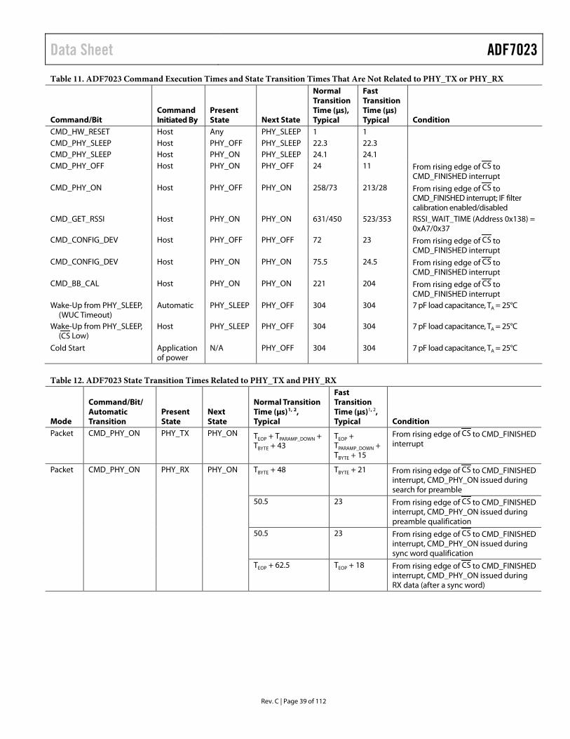
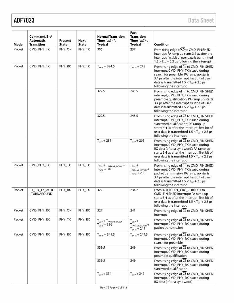
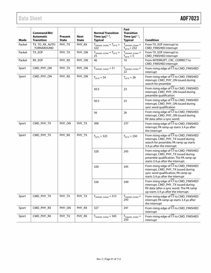
STATE TRANSITION AND COMMAND TIMING The execution times for all radio state transitions are detailed in Table 11 and Table 12. Note that these times are typical and can vary, depending on the BBRAM configuration.
For normal transition times, set TRANSITION_CLOCK_DIV (Location 0x13A) to 0x04. For fast transition times, set TRANSITION_CLOCK_DIV to 0x01. It is recommended to enable fast transition times to reduce system power consumption. As stated in the SPI Interface section, commands are executed on the last positive SCLK edge of the command. For the values given in Table 11 and Table 12, there is an additional 200 ns between the last positive SCLK edge and the rising edge of CS that is related to the SPI rate used.
Data Sheet ADF7023
Rev. C | Page 39 of 112
Table 11. ADF7023 Command Execution Times and State Transition Times That Are Not Related to PHY_TX or PHY_RX
Command/Bit Command Initiated By
Present State Next State
Normal Transition Time (µs), Typical
Fast Transition Time (μs) Typical Condition
CMD_HW_RESET Host Any PHY_SLEEP 1 1 CMD_PHY_SLEEP Host PHY_OFF PHY_SLEEP 22.3 22.3 CMD_PHY_SLEEP Host PHY_ON PHY_SLEEP 24.1 24.1 CMD_PHY_OFF Host PHY_ON PHY_OFF 24 11 From rising edge of CS to
CMD_FINISHED interrupt CMD_PHY_ON Host PHY_OFF PHY_ON 258/73 213/28 From rising edge of CS to
CMD_FINISHED interrupt; IF filter calibration enabled/disabled
Packet CMD_PHY_ON PHY_RX PHY_ON TBYTE + 48 TBYTE + 21 From rising edge of CS to CMD_FINISHED interrupt, CMD_PHY_ON issued during search for preamble
50.5 23 From rising edge of CS to CMD_FINISHED interrupt, CMD_PHY_ON issued during preamble qualification
50.5 23 From rising edge of CS to CMD_FINISHED interrupt, CMD_PHY_ON issued during sync word qualification
TEOP + 62.5 TEOP + 18 From rising edge of CS to CMD_FINISHED interrupt, CMD_PHY_ON issued during RX data (after a sync word)
ADF7023 Data Sheet
Rev. C | Page 40 of 112
Mode
Command/Bit/ Automatic Transition
Present State
Next State
Normal Transition Time (μs)1, 2, Typical
Fast Transition Time (μs)1, 2, Typical Condition
Packet CMD_PHY_TX PHY_ON PHY_TX 306 237 From rising edge of CS to CMD_FINISHED interrupt; PA ramp up starts 3.4 µs after the interrupt; first bit of user data is transmitted 1.5 × TBIT + 2.3 µs following the interrupt
Packet CMD_PHY_TX PHY_RX PHY_TX TBYTE + 324.5 TBYTE + 248 From rising edge of CS to CMD_FINISHED interrupt, CMD_PHY_TX issued during search for preamble; PA ramp up starts 3.4 µs after the interrupt; first bit of user data is transmitted 1.5 × TBIT + 2.3 µs following the interrupt
322.5 245.5 From rising edge of CS to CMD_FINISHED interrupt, CMD_PHY_TX issued during preamble qualification; PA ramp up starts 3.4 µs after the interrupt; first bit of user data is transmitted 1.5 × TBIT + 2.3 µs following the interrupt
322.5 245.5 From rising edge of CS to CMD_FINISHED interrupt, CMD_PHY_TX issued during sync word qualification; PA ramp up starts 3.4 µs after the interrupt; first bit of user data is transmitted 1.5 × TBIT + 2.3 µs following the interrupt
TEOP + 281 TEOP + 263 From rising edge of CS to CMD_FINISHED interrupt, CMD_PHY_TX issued during RX data (after a sync word); PA ramp up starts 3.4 µs after the interrupt; first bit of user data is transmitted 1.5 × TBIT + 2.3 µs following the interrupt
From rising edge of CS to CMD_FINISHED interrupt. CMD_PHY_TX issued during packet transmission; PA ramp up starts 3.4 µs after the interrupt; first bit of user data is transmitted 1.5 × TBIT + 2.3 µs following the interrupt
Packet RX_TO_TX_AUTO_TURNAROUND
PHY_RX PHY_TX 322 234.2 From INTERRUPT_CRC_CORRECT to CMD_FINISHED interrupt; PA ramp up starts 3.4 µs after the interrupt; first bit of user data is transmitted 1.5 × TBIT + 2.3 µs following the interrupt
Packet CMD_PHY_RX PHY_ON PHY_RX 327 241 From rising edge of CS to CMD_FINISHED interrupt
From rising edge of CS to CMD_FINISHED interrupt; CMD_PHY_RX issued during packet transmission
Packet CMD_PHY_RX PHY_RX PHY_RX TBYTE + 341.5 TBYTE + 249.5 From rising edge of CS to CMD_FINISHED interrupt, CMD_PHY_RX issued during search for preamble
339.5 249 From rising edge of CS to CMD_FINISHED interrupt, CMD_PHY_RX issued during preamble qualification
339.5 249 From rising edge of CS to CMD_FINISHED interrupt, CMD_PHY_RX issued during sync word qualification
TEOP + 354 TEOP + 246 From rising edge of CS to CMD_FINISHED interrupt, CMD_PHY_RX issued during RX data (after a sync word)
Packet RX_EOF PHY_RX PHY_ON 46 10 From INTERRUPT_CRC_CORRECT to CMD_FINISHED interrupt
Sport CMD_PHY_ON PHY_TX PHY_ON TPARAMP_DOWN + 51 TPARAMP_DOWN + 22
From rising edge of CS to CMD_FINISHED interrupt
Sport CMD_PHY_ON PHY_RX PHY_ON TBYTE + 54 TBYTE + 28 From rising edge of CS to CMD_FINISHED interrupt, CMD_PHY_ON issued during search for preamble
50.5 23 From rising edge of CS to CMD_FINISHED interrupt, CMD_PHY_ON issued during preamble qualification
50.5 23 From rising edge of CS to CMD_FINISHED interrupt, CMD_PHY_ON issued during sync word qualification
56 26 From rising edge of CS to CMD_FINISHED interrupt, CMD_PHY_ON issued during RX data (after a sync word)
Sport CMD_PHY_TX PHY_ON PHY_TX 306 237 From rising edge of CS to CMD_FINISHED interrupt; PA ramp up starts 3.4 µs after the interrupt
Sport CMD_PHY_TX PHY_RX PHY_TX TBYTE + 325 TBYTE + 250 From rising edge of CS to CMD_FINISHED interrupt, CMD_PHY_TX issued during search for preamble; PA ramp up starts 3.4 µs after the interrupt
320 245 From rising edge of CS to CMD_FINISHED interrupt, CMD_PHY_TX issued during preamble qualification. The PA ramp up starts 3.4 µs after the interrupt.
320 245 From rising edge of CS to CMD_FINISHED interrupt, CMD_PHY_TX issued during sync word qualification; PA ramp up starts 3.4 µs after the interrupt
326 249 From rising edge of CS to CMD_FINISHED interrupt, CMD_PHY_TX issued during RX data (after a sync word). The PA ramp up starts 3.4 µs after the interrupt.
Sport CMD_PHY_TX PHY_TX PHY_TX TPARAMP_DOWN + 315 TPARAMP_DOWN + 243
From rising edge of CS to CMD_FINISHED interrupt; PA ramp up starts 3.4 µs after the interrupt
Sport CMD_PHY_RX PHY_ON PHY_RX 327 241 From rising edge of CS to CMD_FINISHED interrupt
Sport CMD_PHY_RX PHY_TX PHY_RX TPARAMP_DOWN + 345 TPARAMP_DOWN + 250
From rising edge of CS to CMD_FINISHED interrupt
ADF7023 Data Sheet
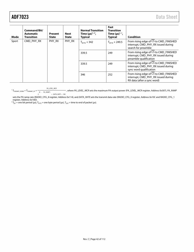
Rev. C | Page 42 of 112
Mode
Command/Bit/ Automatic Transition
Present State
Next State
Normal Transition Time (μs)1, 2, Typical
Fast Transition Time (μs)1, 2, Typical Condition
Sport CMD_PHY_RX PHY_RX PHY_RX TBYTE + 342 TBYTE + 249.5 From rising edge of CS to CMD_FINISHED interrupt, CMD_PHY_RX issued during search for preamble
339.5 249 From rising edge of CS to CMD_FINISHED interrupt, CMD_PHY_RX issued during preamble qualification
339.5 249 From rising edge of CS to CMD_FINISHED interrupt, CMD_PHY_RX issued during sync word qualification
346 252 From rising edge of CS to CMD_FINISHED interrupt, CMD_PHY_RX issued during RX data (after a sync word)
1 TPARAMP_DOWN = TPARAMP_UP =
100)(9
2 ××−
DATA_RATEPA_RAMP
CRPA_LEVEL_M
, where PA_LEVEL_MCR sets the maximum PA output power (PA_LEVEL_MCR register, Address 0x307), PA_RAMP
sets the PA ramp rate (RADIO_CFG_8 register, Address 0x114), and DATA_RATE sets the transmit data rate (RADIO_CFG_0 register, Address 0x10C and RADIO_CFG_1 register, Address 0x10D).
2 TBIT = one bit period (µs), TBYTE = one byte period (µs), TEOP = time to end of packet (µs).
Data Sheet ADF7023
Rev. C | Page 43 of 112
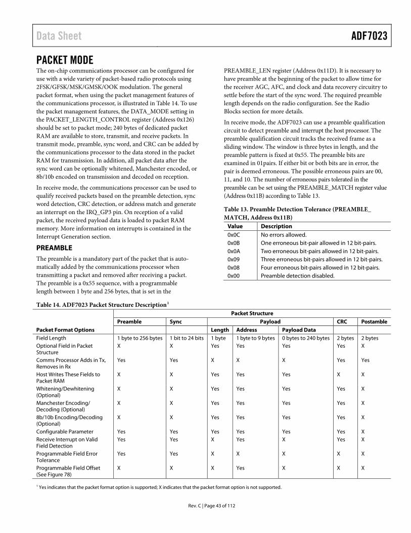
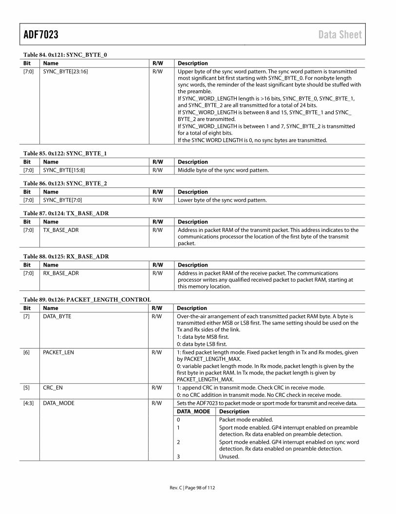
PACKET MODE The on-chip communications processor can be configured for use with a wide variety of packet-based radio protocols using 2FSK/GFSK/MSK/GMSK/OOK modulation. The general packet format, when using the packet management features of the communications processor, is illustrated in Table 14. To use the packet management features, the DATA_MODE setting in the PACKET_LENGTH_CONTROL register (Address 0x126) should be set to packet mode; 240 bytes of dedicated packet RAM are available to store, transmit, and receive packets. In transmit mode, preamble, sync word, and CRC can be added by the communications processor to the data stored in the packet RAM for transmission. In addition, all packet data after the sync word can be optionally whitened, Manchester encoded, or 8b/10b encoded on transmission and decoded on reception.
In receive mode, the communications processor can be used to qualify received packets based on the preamble detection, sync word detection, CRC detection, or address match and generate an interrupt on the IRQ_GP3 pin. On reception of a valid packet, the received payload data is loaded to packet RAM memory. More information on interrupts is contained in the Interrupt Generation section.
PREAMBLE The preamble is a mandatory part of the packet that is auto-matically added by the communications processor when transmitting a packet and removed after receiving a packet. The preamble is a 0x55 sequence, with a programmable length between 1 byte and 256 bytes, that is set in the
PREAMBLE_LEN register (Address 0x11D). It is necessary to have preamble at the beginning of the packet to allow time for the receiver AGC, AFC, and clock and data recovery circuitry to settle before the start of the sync word. The required preamble length depends on the radio configuration. See the Radio Blocks section for more details.
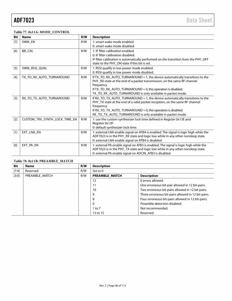
In receive mode, the ADF7023 can use a preamble qualification circuit to detect preamble and interrupt the host processor. The preamble qualification circuit tracks the received frame as a sliding window. The window is three bytes in length, and the preamble pattern is fixed at 0x55. The preamble bits are examined in 01pairs. If either bit or both bits are in error, the pair is deemed erroneous. The possible erroneous pairs are 00, 11, and 10. The number of erroneous pairs tolerated in the preamble can be set using the PREAMBLE_MATCH register value (Address 0x11B) according to Table 13.
Value Description 0x0C No errors allowed. 0x0B One erroneous bit-pair allowed in 12 bit-pairs.
0x0A Two erroneous bit-pairs allowed in 12 bit-pairs.
0x09 Three erroneous bit-pairs allowed in 12 bit-pairs.
0x08 Four erroneous bit-pairs allowed in 12 bit-pairs.
0x00 Preamble detection disabled.
Table 14. ADF7023 Packet Structure Description1
Packet Format Options
Packet Structure
Preamble Sync Payload CRC Postamble
Length Address Payload Data
Field Length 1 byte to 256 bytes 1 bit to 24 bits 1 byte 1 byte to 9 bytes 0 bytes to 240 bytes 2 bytes 2 bytes Optional Field in Packet Structure
X X Yes Yes Yes Yes X
Comms Processor Adds in Tx, Removes in Rx
Yes Yes X X X Yes Yes
Host Writes These Fields to Packet RAM
X X Yes Yes Yes X X
Whitening/Dewhitening (Optional)
X X Yes Yes Yes Yes X
Manchester Encoding/ Decoding (Optional)
X X Yes Yes Yes Yes X
8b/10b Encoding/Decoding (Optional)
X X Yes Yes Yes Yes X
Configurable Parameter Yes Yes Yes Yes Yes Yes X Receive Interrupt on Valid Field Detection
Yes Yes X Yes X Yes X
Programmable Field Error Tolerance
Yes Yes X X X X X
Programmable Field Offset (See Figure 78)
X X X Yes X X X
1 Yes indicates that the packet format option is supported; X indicates that the packet format option is not supported.
ADF7023 Data Sheet
Rev. C | Page 44 of 112
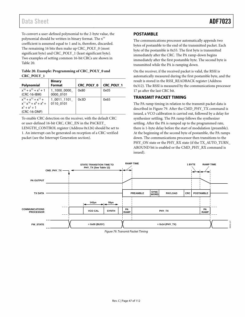
If PREAMBLE_MATCH is set to 0x0C, the ADF7023 must receive 12 consecutive 01 pairs (three bytes) to confirm that valid preamble has been detected. The user can select the option to automatically lock the AFC and/or AGC once the qualified preamble is detected. The AFC lock on preamble detection can be enabled by setting AFC_LOCK_MODE = 3 in the RADIO_CFG_10 register (Address 0x116:). The AGC lock on preamble detection can be enabled by setting AGC_LOCK_ MODE = 3 in the RADIO_CFG_7 register (Address 0x113).
After the preamble is detected and the end of preamble has been reached, the communications processor searches for the sync word. The search for the sync word lasts for a duration equal to the sum of the number of programmed sync word bits, plus the preamble matching tolerance (in bits) plus 16 bits. If the sync word routine is detected during this duration, the communications processor loads the received payload to packet RAM and computes the CRC (if enabled). If the sync word routine is not detected during this duration, the communications processor continues searching for the preamble.
Preamble detection can be disabled by setting the PREAMBLE_ MATCH register to 0x00. To enable an interrupt upon preamble detection, the user must set INTERRUPT_PREAMBLE_DETECT =1 in the INTERRUPT_MASK_0 register (Address 0x100).
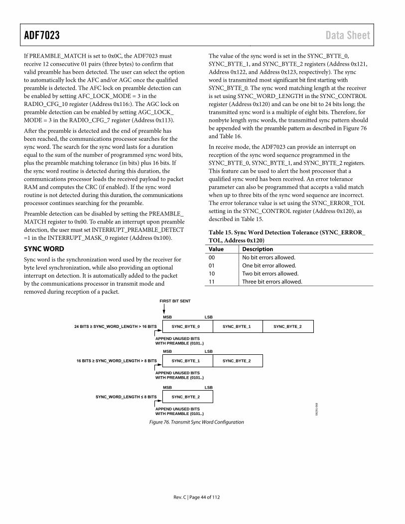
SYNC WORD Sync word is the synchronization word used by the receiver for byte level synchronization, while also providing an optional interrupt on detection. It is automatically added to the packet by the communications processor in transmit mode and removed during reception of a packet.
The value of the sync word is set in the SYNC_BYTE_0, SYNC_BYTE_1, and SYNC_BYTE_2 registers (Address 0x121, Address 0x122, and Address 0x123, respectively). The sync word is transmitted most significant bit first starting with SYNC_BYTE_0. The sync word matching length at the receiver is set using SYNC_WORD_LENGTH in the SYNC_CONTROL register (Address 0x120) and can be one bit to 24 bits long; the transmitted sync word is a multiple of eight bits. Therefore, for nonbyte length sync words, the transmitted sync pattern should be appended with the preamble pattern as described in Figure 76 and Table 16.
In receive mode, the ADF7023 can provide an interrupt on reception of the sync word sequence programmed in the SYNC_BYTE_0, SYNC_BYTE_1, and SYNC_BYTE_2 registers. This feature can be used to alert the host processor that a qualified sync word has been received. An error tolerance parameter can also be programmed that accepts a valid match when up to three bits of the sync word sequence are incorrect. The error tolerance value is set using the SYNC_ERROR_TOL setting in the SYNC_CONTROL register (Address 0x120), as described in Table 15.
Table 15. Sync Word Detection Tolerance (SYNC_ERROR_ TOL, Address 0x120) Value Description 00 No bit errors allowed. 01 One bit error allowed. 10 Two bit errors allowed.
The sync word should be chosen to have low correlation with the preamble and have good autocorrelation properties. When the AFC is set to lock on detection of sync word (AFC_LOCK_ MODE = 3 and PREAMBLE_MATCH = 0), the sync word should be chosen to be dc free, and it should have a run length limit not greater than four bits.
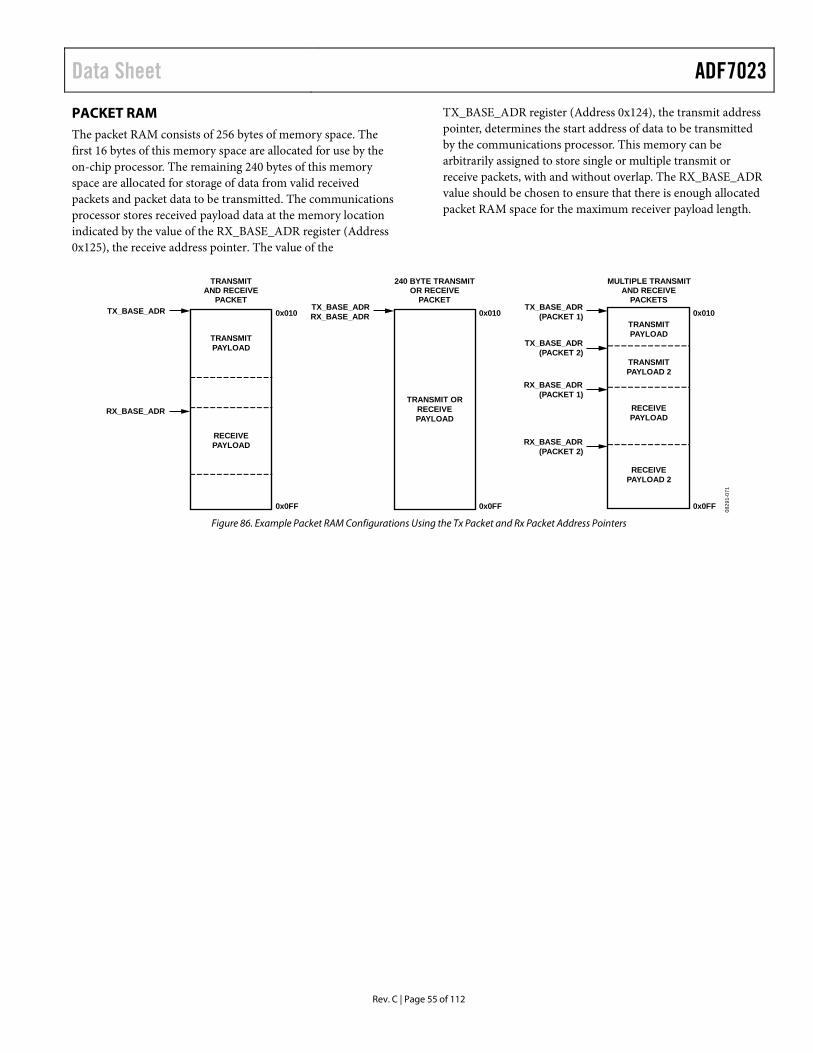
PAYLOAD The host processor writes the transmit data payload to the packet RAM. The location of the transmit data in the packet RAM is defined by the TX_BASE_ADR value register (Address 0x124). The TX_BASE_ADR value is the location of the first byte of the transmit payload data in the packet RAM. On reception of a valid sync word, the communications processor automatically loads the receive payload to the packet RAM. The RX_BASE_ADR register value (Address 0x125) sets the location in the packet RAM of the first byte of the received payload. For more details on packet RAM memory, see the ADF7023 Memory Map section.
Byte Orientation
The over-the-air arrangement of each transmitted packet RAM byte can be set to MSB first or LSB first using the DATA_BYTE setting in the PACKET_LENGTH_CONTROL register (Address 0x126). The same orientation setting should be used on the transmit and receive sides of the RF link.
Packet Length Modes
The ADF7023 can be used in both fixed and variable length packet systems. Fixed or variable length packet mode is set using the PACKET_LEN variable setting in the PACKET_ LENGTH_CONTROL register (Address 0x126).
For a fixed packet length system, the length of the transmit and received payload is set by the PACKET_LENGTH_MAX register (Address 0x127). The payload length is defined as the number of bytes from the end of the sync word to the start of the CRC.
In variable packet length mode, the communications processor extracts the length field from the received payload data. In transmit mode, the length field must be the first byte in the transmit payload.
The communications processor calculates the actual received payload length as
RxPayload Length = Length + LENGTH_OFFSET − 4
where: Length is the length field (the first byte in the received payload). LENGTH_OFFSET is a programmable offset (set in the PACKET_LENGTH_CONTROL register (Address 0x126).
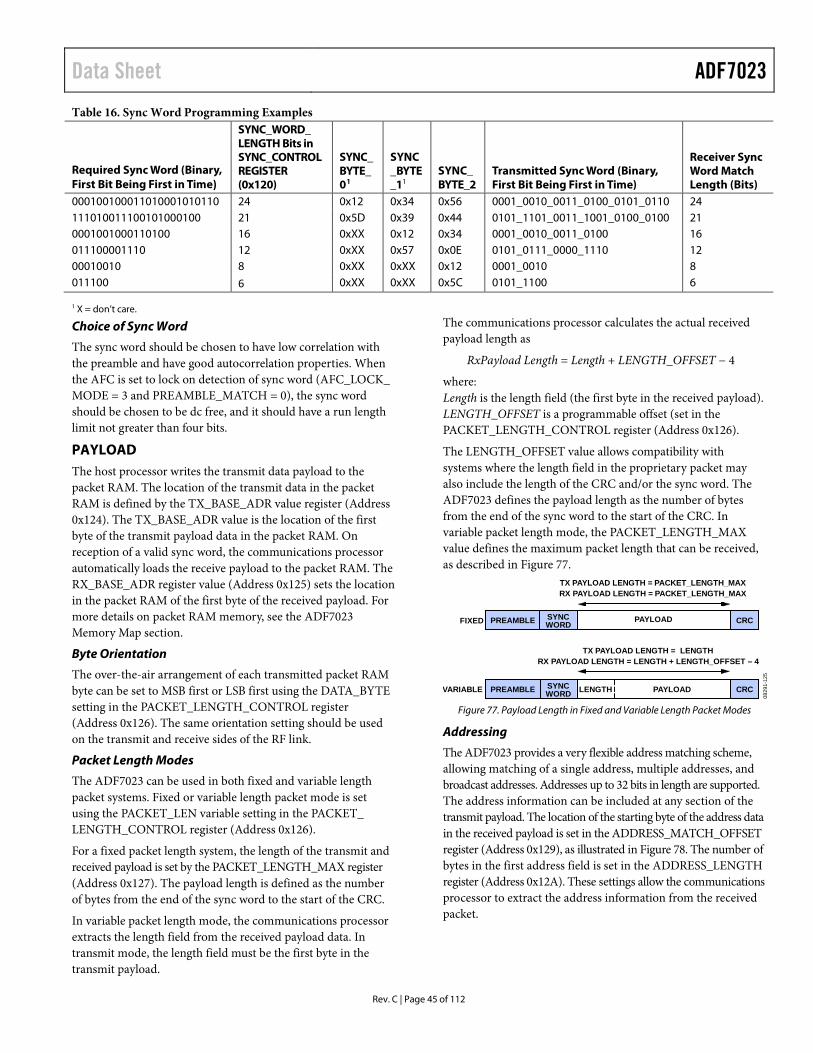
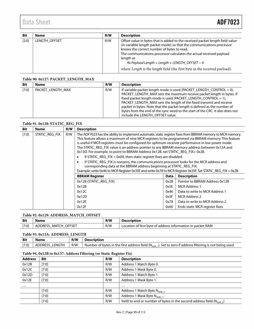
The LENGTH_OFFSET value allows compatibility with systems where the length field in the proprietary packet may also include the length of the CRC and/or the sync word. The ADF7023 defines the payload length as the number of bytes from the end of the sync word to the start of the CRC. In variable packet length mode, the PACKET_LENGTH_MAX value defines the maximum packet length that can be received, as described in Figure 77.
Figure 77. Payload Length in Fixed and Variable Length Packet Modes
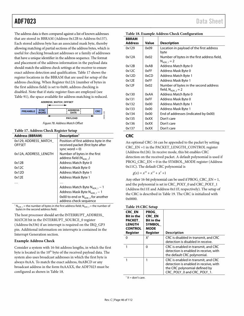
Addressing
The ADF7023 provides a very flexible address matching scheme, allowing matching of a single address, multiple addresses, and broadcast addresses. Addresses up to 32 bits in length are supported. The address information can be included at any section of the transmit payload. The location of the starting byte of the address data in the received payload is set in the ADDRESS_MATCH_OFFSET register (Address 0x129), as illustrated in Figure 78. The number of bytes in the first address field is set in the ADDRESS_LENGTH register (Address 0x12A). These settings allow the communications processor to extract the address information from the received packet.
The address data is then compared against a list of known addresses that are stored in BBRAM (Address 0x12B to Address 0x137). Each stored address byte has an associated mask byte, thereby allowing matching of partial sections of the address bytes, which is useful for checking broadcast addresses or a family of addresses that have a unique identifier in the address sequence. The format and placement of the address information in the payload data should match the address check settings at the receiver to ensure exact address detection and qualification. Table 17 shows the register locations in the BBRAM that are used for setup of the address checking. When Register 0x12A (number of bytes in the first address field) is set to 0x00, address checking is disabled. Note that if static register fixes are employed (see Table 91), the space available for address matching is reduced.
Position of first address byte in the received packet (first byte after sync word = 0)
0x12A, ADDRESS_LENGTH Number of bytes in the first address field (NADR_1)
0x12B Address Match Byte 0 0x12C Address Mask Byte 0 0x12D Address Match Byte 1 0x12E Address Mask Byte 1 … … Address Match Byte NADR_1 − 1 Address Mask Byte NADR_1 − 1 0x00 to end or NADR_2 for another
address check sequence 1 NADR_1 = the number of bytes in the first address field; NADR_2 = the number of
bytes in the second address field.
The host processor should set the INTERRUPT_ADDRESS_ MATCH bit in the INTERRUPT_SOURCE_0 register (Address 0x336) if an interrupt is required on the IRQ_GP3 pin. Additional information on interrupts is contained in the Interrupt Generation section.
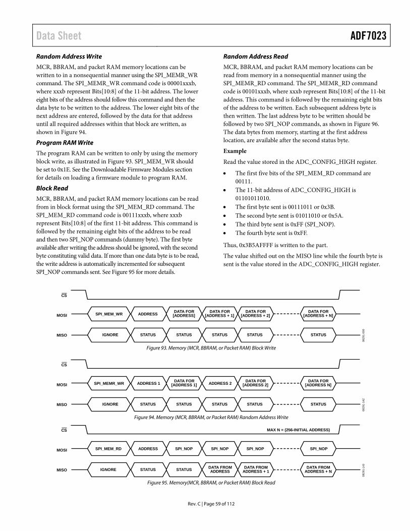
Example Address Check
Consider a system with 16-bit address lengths, in which the first byte is located in the 10th byte of the received payload data. The system also uses broadcast addresses in which the first byte is always 0xAA. To match the exact address, 0xABCD or any broadcast address in the form 0xAAXX, the ADF7023 must be configured as shown in Table 18.
Table 18. Example Address Check Configuration BBRAM Address Value Description 0x129 0x09 Location in payload of the first address
byte 0x12A 0x02 Number of bytes in the first address field,
NADR_1 = 2 0x12B 0xAB Address Match Byte 0 0x12C 0xFF Address Mask Byte 0 0x12D 0xCD Address Match Byte 1 0x12E 0xFF Address Mask Byte 1 0x12F 0x02 Number of bytes in the second address
field, NADR_2 = 2 0x130 0xAA Address Match Byte 0 0x131 0xFF Address Mask Byte 0 0x132 0x00 Address Match Byte 1 0x133 0x00 Address Mask Byte 1 0x134 0x00 End of addresses (indicated by 0x00) 0x135 0xXX Don’t care 0x136 0xXX Don’t care 0x137 0xXX Don’t care
CRC An optional CRC-16 can be appended to the packet by setting CRC_EN =1 in the PACKET_LENGTH_CONTROL register (Address 0x126). In receive mode, this bit enables CRC detection on the received packet. A default polynomial is used if PROG_CRC_EN = 0 in the SYMBOL_MODE register (Address 0x11C). The default CRC polynomial is
g(x) = x16 + x12 + x5 +1
Any other 16-bit polynomial can be used if PROG_CRC_EN = 1, and the polynomial is set in CRC_POLY_0 and CRC_POLY_1 (Address 0x11E and Address 0x11F, respectively). The setup of the CRC is described in Table 19. The CRC is initialized with 0x0000.
Table 19.CRC Setup CRC_EN Bit in the PACKET_LENGTH CONTROL Register
PROG_ CRC_EN Bit in the SYMBOL_MODE Register Description
0 X1 CRC is disabled in transmit, and CRC detection is disabled in receive.
1 0 CRC is enabled in transmit, and CRC detection is enabled in receive, with the default CRC polynomial.
1 1 CRC is enabled in transmit, and CRC detection is enabled in receive, with the CRC polynomial defined by CRC_POLY_0 and CRC_POLY_1.
1 X = don’t care.
0829
1-12
6ADDRESS_MATCH_OFFSET
PREAMBLE SYNCWORD
ADDRESSDATA
PAYLOAD
CRC
Data Sheet ADF7023
Rev. C | Page 47 of 112
To convert a user-defined polynomial to the 2-byte value, the polynomial should be written in binary format. The x16 coefficient is assumed equal to 1 and is, therefore, discarded. The remaining 16 bits then make up CRC_POLY_0 (most significant byte) and CRC_POLY_1 (least significant byte). Two examples of setting common 16-bit CRCs are shown in Table 20.
Table 20. Example: Programming of CRC_POLY_0 and CRC_POLY_1
To enable CRC detection on the receiver, with the default CRC or user-defined 16-bit CRC, CRC_EN in the PACKET_ LENGTH_CONTROL register (Address 0x126) should be set to 1. An interrupt can be generated on reception of a CRC verified packet (see the Interrupt Generation section).
POSTAMBLE The communications processor automatically appends two bytes of postamble to the end of the transmitted packet. Each byte of the postamble is 0x55. The first byte is transmitted immediately after the CRC. The PA ramp-down begins immediately after the first postamble byte. The second byte is transmitted while the PA is ramping down.
On the receiver, if the received packet is valid, the RSSI is automatically measured during the first postamble byte, and the result is stored in the RSSI_READBACK register (Address 0x312). The RSSI is measured by the communications processor 17 μs after the last CRC bit.
TRANSMIT PACKET TIMING The PA ramp timing in relation to the transmit packet data is described in Figure 79. After the CMD_PHY_TX command is issued, a VCO calibration is carried out, followed by a delay for synthesizer settling. The PA ramp follows the synthesizer settling. After the PA is ramped up to the programmed rate, there is 1-byte delay before the start of modulation (preamble). At the beginning of the second byte of postamble, the PA ramps down. The communications processor then transitions to the PHY_ON state or the PHY_RX state (if the TX_AUTO_TURN_ AROUND bit is enabled or the CMD_PHY_RX command is issued).
Figure 79. Transmit Packet Timing
142µs 55µs
VCO CAL SYNTH
PREAMBLE SYNCWORD CRC POSTAMBLEPAYLOAD
PHY_TX
= 0x14 (PHY_TX)= 0x00 (BUSY)
PARAMP
PARAMP
1 BYTE RAMP TIMERAMP TIMESTATE TRANSITION TIME TOPHY_TX (See Table 12)
CMD_PHY_TX
PA OUTPUT
TX DATA
COMMUNICATIONSPROCESSOR
FW_STATE
0829
1-12
7
ADF7023 Data Sheet
Rev. C | Page 48 of 112
DATA WHITENING Data whitening can be employed to avoid long runs of 1s or 0s in the transmitted data stream. This ensures sufficient bit transitions in the packet, which aids in receiver clock and data recovery because the encoding breaks up long runs of 1s or 0s in the transmit packet. The data, excluding the preamble and sync word, is automatically whitened before transmission by XOR’ing the data with an 8-bit pseudorandom sequence. At the receiver, the data is XOR’ed with the same pseudorandom sequence, thereby reversing the whitening. The linear feedback shift register polynomial used is x7 + x1 + 1. Data whitening and dewhitening are enabled by setting DATA_WHITENING = 1 in the SYMBOL_MODE register (Address 0x11C).
MANCHESTER ENCODING Manchester encoding can be used to ensure a dc-free (zero mean) transmission. The encoded over-the-air bit rate (chip rate) is double the rate set by the DATA_RATE variable (Address 0x10C and Address 0x10D). A Binary 0 is mapped to 10, and a Binary 1 is mapped to 01. Manchester encoding and decoding are applied to the payload data and the CRC. It is recommended to use Manchester encoding for OOK modu-lation. Manchester encoding and decoding are enabled by setting MANCHESTER_ENC = 1 in the SYMBOL_MODE register (Address 0x11C).
8B/10B ENCODING 8b/10b encoding is a byte-orientated encoding scheme that maps an 8-bit byte to a 10-bit data block. It ensures that the maximum number of consecutive 1s or 0s (that is, run length) in any 10-bit transmitted symbol is five. The advantage of this encoding scheme is that dc balancing is employed without the efficiency loss of Manchester encoding. The rate loss for 8b/10b encoding is 0.8, whereas for Manchester encoding, it is 0.5. Encoding and decoding are applied to the payload data and the CRC. The 8b/10b encoding and decoding are enabled by setting EIGHT_TEN_ENC =1 in the SYMBOL_MODE register (Address 0x11C).
Data Sheet ADF7023
Rev. C | Page 49 of 112
SPORT MODE It is possible to bypass all of the packet management features of the ADF7023 and use the sport interface for transmit and receive data. The sport interface is a high speed synchronous serial interface allowing direct interfacing to processors and DSPs. Sport mode is enabled using the DATA_MODE setting in the PACKET_LENGTH_CONTROL register (Address 0x126), as described in Table 21. The sport mode interface is on the GPIO pins (GP0, GP1, GP2, GP4, and XOSC32KP_GP5_ATB1). These GPIO pins can be configured using the GPIO_CONFIGURE setting (Address 0x3FA), as described in Table 22.
Sport mode provides a receive interrupt source on GP4. This interrupt source can be configured to provide an interrupt, or strobe signal, on either preamble detection or sync word detection. The type of interrupt is configured using the GPIO_CONFIGURE setting.
PACKET STRUCTURE IN SPORT MODE In sport mode, the host processor has full control over the packet structure. However, the preamble frame is still required to allow sufficient bits for receiver settling (AGC, AFC, and CDR). In sport mode, sync word detection is not mandatory in the ADF7023 but can be enabled to provide byte level synchronization for the host processor via the sync word detect interrupt or strobe on GP4. The general format of a sport mode packet is shown in Figure 80.
Figure 80. General Sport Mode Packet
SPORT MODE IN TRANSMIT Figure 81 illustrates the operation of the sport interface in transmit. Once in the PHY_TX state with sport mode enabled, the data input of the transmitter is fully controlled by the sport
interface (Pin GP1). The transmit clock appears on the GP2 pin. The transmit data from the host processor should be synch-ronized with this clock. The FW_STATE variable in the status word or the CMD_FINISHED interrupt can be used to indicate when the ADF7023 has reached the PHY_TX state and, there-fore, is ready to begin transmitting data. The ADF7023 keeps transmitting the serial data presented at the GP1 input until the host processor issues a command to exit the PHY_TX state.
SPORT MODE IN RECEIVE The sport interface supports the receive operation with a number of modes to suit particular signaling requirements. The receive data appears on the GP0 pin, whereas the receive synchronized clock appears on the GP2 pin. The GP4 pin provides an interrupt or strobe signal on either preamble or sync word detection, as described in Table 21 and Table 22. Once enabled, the interrupt signal and strobe signals remain operational while in the PHY_RX state. The strobe signal gives a single high pulse of 1-bit duration every eight bits. The strobe signal is most useful when used with sync word detection because it is synchronized to the sync word and strobes the first bit in every byte.
TRANSMIT BIT LATENCIES IN SPORT MODE The transmit bit latency is the time from the sampling of a bit by the transmit data clock on GP2 to when that bit appears at the RF output. There is no transmit bit latency when using 2FSK/MSK modulation. The latency when using GFSK/GMSK modulation is two bits. It is important that the host processor keep the ADF7023 in the PHY_TX state for two bit periods after the last data bit is sampled by the data clock to account for this latency when using GMSK/GFSK modulation.
Table 21. SPORT Mode Setup DATA_MODE Bits in PACKET_LENGTH_ CONTROL Register Description GPIO Configuration DATA_MODE = 0 Packet mode enabled. Packet management is
controlled by the communications processor.
DATA_MODE = 1 Sport mode enabled. The Rx data and Rx clock are enabled in the PHY_RX state (GPIO_CONFIGURE = 0xA0, 0xA3, 0xA6). The Rx clock is enabled in the PHY_RX state, and Rx data is enabled on the preamble detect (GPIO_CONFIGURE = 0xA1, 0xA2, 0xA4, 0xA5, 0xA7, 0xA8).
GP0: Rx data GP1: Tx data GP2: Tx/Rx clock GP4: interrupt or strobe enabled on preamble detect (depends on GPIO_CONFIGURE) XOSC32KP_GP5_ATB1: depends on GPIO_CONFIGURE
DATA_MODE = 2 Sport mode enabled. The Rx data and Rx clock are enabled in the PHY_RX state if GPIO_CONFIGURE = 0xA0, 0xA3, 0xA6. The Rx clock is enabled in the PHY_RX state, and Rx data is enabled on the preamble detect if GPIO_CONFIGURE = 0xA1, 0xA2, 0xA4, 0xA5, 0xA7, 0xA8.
GP0: Rx data GP1: Tx data GP2: Tx/Rx clock GP4: interrupt or strobe enabled on sync word detect (depends on GPIO_CONFIGURE) XOSC32KP_GP5_ATB1: depends on GPIO_CONFIGURE
0829
1-12
8
PREAMBLE SYNCWORD PAYLOAD
ADF7023 Data Sheet
Rev. C | Page 50 of 112
Table 22. GPIO Functionality in Sport Mode GPIO_CONFIGURE GP0 GP1 GP2 GP4 XOSC32KP_GP5_ATB1 0xA0 Rx data Tx data Tx/Rx clock Not used Not used 0xA1 Rx data Tx data Tx/Rx clock Interrupt Not used 0xA2 Rx data Tx data Tx/Rx clock Strobe Not used 0xA3 Rx data Tx data Tx/Rx clock Not used 32.768 kHz XTAL input 0xA4 Rx data Tx data Tx/Rx clock Interrupt 32.768 kHz XTAL input 0xA5 Rx data Tx data Tx/Rx clock Strobe 32.768 kHz XTAL input 0xA6 Rx data Tx data Tx/Rx clock Not used EXT_UC_CLK output 0xA7 Rx data Tx data Tx/Rx clock Interrupt EXT_UC_CLK output 0xA8 Rx data Tx data Tx/Rx clock Strobe EXT_UC_CLK output
Figure 81. Sport Mode Transmit
Figure 82. Sport Mode Receive, DATA_MODE = 1, 2 and GPIO_CONFIGURE = 0xA0, 0xA3, 0xA6
INTERRUPT GENERATION The ADF7023 uses a highly flexible, powerful interrupt system with support for MAC level interrupts and PHY level interrupts. To enable an interrupt source, the corresponding mask bit must be set. When an enabled interrupt occurs, the IRQ_GP3 pin goes high, and the interrupt bit of the status word is set to Logic 1. The host processor can use either the IRQ_GP3 pin or the status word to check for an interrupt. After an interrupt is asserted, the ADF7023 continues operations unaffected, unless it is directed to do otherwise by the host processor. An outline of the interrupt source and mask system is shown in Table 23.
MAC interrupts can be enabled by writing a Logic 1 to the relevant bits of the INTERRUPT_MASK_0 register (Address 0x100) and PHY level interrupts by writing a Logic 1 to the relevant bits of the INTERRUPT_MASK_1 register (Address 0x101). The structure of these memory locations is described in Table 23.
In the case of an interrupt condition, the interrupt source can be determined by reading the INTERRUPT_SOURCE_0 register (Address 0x336) and the INTERRUPT_SOURCE_1 register (Address 0x337). The bit that corresponds to the relevant
interrupt condition is high. The structure of these two registers is shown in Table 24.
Following an interrupt condition, the host processor should clear the relevant interrupt flag so that further interrupts assert the IRQ_GP3 pin. This is performed by writing a Logic 1 to the bit that is high in either the INTERRUPT_SOURCE_0 or INTERRUPT_SOURCE_1 register. If multiple bits in the interrupt source registers are high, they can be cleared individually or altogether by writing Logic 1 to them. The IRQ_GP3 pin goes low when all the interrupt source bits are cleared.
As an example, take the case where a battery alarm (in the INTERRUPT_SOURCE_1 register) interrupt occurs. The host processor should
1. Read the interrupt source registers. In this example, if none of the interrupt flags in INTERRUPT_SOURCE_0 is enabled, only INTERRUPT_SOURCE_1 must be read.
2. Clear the interrupt by writing 0x80 (or 0xFF) to INTERRUPT_SOURCE_1.
3. Respond to the interrupt condition.
Table 23. Structure of the Interrupt Mask Registers Register Bit Name Description INTERRUPT_MASK_0, Address 0x100
7 INTERRUPT_NUM_WAKEUPS Interrupt when the number of WUC wake-ups (NUMBER_OF_WAKEUPS[15:0]) has reached the threshold (NUMBER_OF_WAKEUPS_IRQ_THRESHOLD[15:0]) 1: interrupt enabled; 0: interrupt disabled
6 INTERRUPT_SWM_RSSI_DET Interrupt when the measured RSSI during smart wake mode has exceeded the RSSI threshold value (SWM_RSSI_THRESH, Address 0x108) 1: interrupt enabled; 0: interrupt disabled
5 INTERRUPT_AES_DONE Interrupt when an AES encryption or decryption command is complete; available only when the AES firmware module has been loaded to the ADF7023 program RAM 1: interrupt enabled; 0: interrupt disabled
4 INTERRUPT_TX_EOF Interrupt when a packet has finished transmitting 1: interrupt enabled; 0: interrupt disabled
3 INTERRUPT_ADDRESS_MATCH Interrupt when a received packet has a valid address match 1: interrupt enabled; 0: interrupt disabled
2 INTERRUPT_CRC_CORRECT Interrupt when a received packet has the correct CRC 1: interrupt enabled; 0: interrupt disabled
1 INTERRUPT_SYNC_DETECT Interrupt when a qualified sync word has been detected in the received packet 1: interrupt enabled; 0: interrupt disabled
0 INTERRUPT_PREAMBLE_DETECT Interrupt when a qualified preamble has been detected in the received packet 1: interrupt enabled; 0: interrupt disabled
Data Sheet ADF7023
Rev. C | Page 53 of 112
Register Bit Name Description INTERRUPT_MASK_1, Address 0x101
7 BATTERY_ALARM Interrupt when the battery voltage has dropped below the threshold value (BATTERY_MONITOR_THRESHOLD_VOLTAGE, Address 0x32D) 1: interrupt enabled; 0: interrupt disabled
6 CMD_READY Interrupt when the communications processor is ready to load a new command; mirrors the CMD_READY bit of the status word 1: interrupt enabled; 0: interrupt disabled
5 Reserved
4 WUC_TIMEOUT Interrupt when the WUC has timed out 1: interrupt enabled; 0: interrupt disabled
3 Reserved 2 Reserved 1 SPI_READY Interrupt when the SPI is ready for access
1: interrupt enabled; 0: interrupt disabled 0 CMD_FINISHED Interrupt when the communications processor has finished
performing a command 1: interrupt enabled; 0: interrupt disabled
Table 24. Structure of the Interrupt Source Registers Register Bit Name Interrupt Description INTERRUPT_SOURCE_0, Address: 0x336
7 INTERRUPT_NUM_WAKEUPS Asserted when the number of WUC wake-ups (NUMBER_OF_WAKEUPS[15:0]) has reached the threshold (NUMBER_OF_WAKEUPS_IRQ_THRESHOLD[15:0]).
6 INTERRUPT_SWM_RSSI_DET Asserted when the measured RSSI during smart wake mode has exceeded the RSSI threshold value (SWM_RSSI_THRESH, Address 0x108).
5 INTERRUPT_AES_DONE Asserted when an AES encryption or decryption command is complete; available only when the AES firmware module has been loaded to the ADF7023 program RAM.
4 INTERRUPT_TX_EOF Asserted when a packet has finished transmitting (packet mode only). 3 INTERRUPT_ADDRESS_MATCH Asserted when a received packet has a valid address match (packet
mode only). 2 INTERRUPT_CRC_CORRECT Asserted when a received packet has the correct CRC (packet mode only). 1 INTERRUPT_SYNC_DETECT Asserted when a qualified sync word has been detected in the
received packet. 0 INTERRUPT_PREAMBLE_DETECT Asserted when a qualified preamble has been detected in the
received packet. INTERRUPT_SOURCE_1, Address: 0x337
7 BATTERY_ALARM Asserted when the battery voltage has dropped below the threshold value (BATTERY_MONITOR_THRESHOLD_VOLTAGE, Address 0x32D).
6 CMD_READY Asserted when the communications processor is ready to load a new command; mirrors the CMD_READY bit of the status word.
5 Reserved 4 WUC_TIMEOUT Asserted when the WUC has timed out. 3 Reserved 2 Reserved 1 SPI_READY Asserted when the SPI is ready for access. 0 CMD_FINISHED Asserted when the communications processor has finished
performing a command. If the CMD_FINISHED interrupt is enabled, following the issue of CMD_PHY_TX, the first bit of user data is transmitted 1.5 × TBIT + 2.3 µs following the interrupt. The PA ramp starts 3.4 µs after the interrupt. (TBIT is the time taken to transmit one bit.)
INTERRUPTS IN SPORT MODE In sport mode, the interrupts from INTERRUPT_SOURCE_1 are all available. However, only INTERRUPT_PREAMBLE_ DETECT and INTERRUPT_SYNC_DETECT are available from INTERRUPT_SOURCE_0. A second interrupt pin is
provided on GP4, which gives a dedicated sport mode interrupt on either preamble or sync word detection. For more details, see the Sport Mode section.
ADF7023 Data Sheet
Rev. C | Page 54 of 112
ADF7023 MEMORY MAP
Figure 85. ADF7023 Memory Map
This section describes the various memory locations used by the ADF7023. The radio control, packet management, and smart wake mode capabilities of the part are realized through the use of an integrated RISC processor, which executes instructions stored in the embedded program ROM. There is also a local RAM, subdivided into three sections, that is used as a data packet buffer, both for transmitted and received data (packet RAM), and for storing the radio and packet management configuration (BBRAM and MCR). The RAM addresses of these memory banks are 11 bits long.
BBRAM The battery backup RAM (BBRAM) contains the main radio and packet management registers used to configure the radio. On application of battery power to the ADF7023 for the first time, the entire BBRAM should be initialized by the host processor with the appropriate settings. After the BBRAM has been written to, the CMD_CONFIG_DEV command should be issued to update the radio and communications processor with the current BBRAM settings. The CMD_CONFIG_DEV command can be issued in the PHY_OFF state or the PHY_ON state only.
The BBRAM is used to maintain settings needed at wake-up from sleep mode by the wake-up controller. Upon wake-up from sleep, in smart wake mode, the BBRAM contents are read by the on-chip processor to recover the packet management and radio parameters.
MODEM CONFIGURATION RAM (MCR) The 256-byte modem configuration RAM (MCR) contains the various registers used for direct control or observation of the physical layer radio blocks of the ADF7023. The contents of the MCR are not retained in the PHY_SLEEP state.
PROGRAM ROM The program ROM consists of 4 kB of nonvolatile memory. It contains the firmware code for radio control, packet manage-ment, and smart wake mode.
PROGRAM RAM The program RAM consists of 2 kB of volatile memory. This memory space is used for software modules, such as AES en-cryption, IR calibration, and Reed Solomon coding, which are available from Analog Devices. The software modules are down-loaded to the program RAM memory space over the SPI by the host processor. See the Downloadable Firmware Modules section for details on loading a firmware module to program RAM.
0829
1-07
0
SPI
CS
MISO
MOSI
SCLK
DATA[7:0]
ADDRESS[10:0]
NOT USED
RESERVED
0x100
0x13F
0x300
0x3FF
0x0FF
0x0000x00F
0x000
ADDRESS[12:0]
PROGRAMRAM2kB
PROGRAMROM4kB
MCR256 BYTES
BBRAM64 BYTES
PACKETRAM
256 BYTES
INSTRUCTION/DATA[7:0]
11-BITADDRESSES
ADDRESS/DATAMUX
SPI/CPMEMORY
ARBITRATION
COMMSPROCESSOR
CLOCK
COMMSPROCESSOR
8-BITRISC
ENGINE
Data Sheet ADF7023
Rev. C | Page 55 of 112
PACKET RAM The packet RAM consists of 256 bytes of memory space. The first 16 bytes of this memory space are allocated for use by the on-chip processor. The remaining 240 bytes of this memory space are allocated for storage of data from valid received packets and packet data to be transmitted. The communications processor stores received payload data at the memory location indicated by the value of the RX_BASE_ADR register (Address 0x125), the receive address pointer. The value of the
TX_BASE_ADR register (Address 0x124), the transmit address pointer, determines the start address of data to be transmitted by the communications processor. This memory can be arbitrarily assigned to store single or multiple transmit or receive packets, with and without overlap. The RX_BASE_ADR value should be chosen to ensure that there is enough allocated packet RAM space for the maximum receiver payload length.
Figure 86. Example Packet RAM Configurations Using the Tx Packet and Rx Packet Address Pointers
TRANSMIT ORRECEIVEPAYLOAD
TRANSMITPAYLOAD
RECEIVEPAYLOAD
TRANSMITPAYLOAD
RECEIVEPAYLOAD
RECEIVEPAYLOAD 2
TRANSMITPAYLOAD 2
MULTIPLE TRANSMITAND RECEIVE
PACKETS
240 BYTE TRANSMITOR RECEIVE
PACKET
TRANSMITAND RECEIVE
PACKET0x010
0x0FF
0x010
0x0FF
0x010
0x0FF
TX_BASE_ADR(PACKET 1)
TX_BASE_ADRRX_BASE_ADR
TX_BASE_ADR
RX_BASE_ADR
TX_BASE_ADR(PACKET 2)
RX_BASE_ADR(PACKET 1)
RX_BASE_ADR(PACKET 2)
0829
1-07
1
ADF7023 Data Sheet
Rev. C | Page 56 of 112
SPI INTERFACE GENERAL CHARACTERISTICS The ADF7023 is equipped with a 4-wire SPI interface, using the SCLK, MISO, MOSI, and CS pins. The ADF7023 always acts as a slave to the host processor. Figure 87 shows an example connection diagram between the processor and the ADF7023. The diagram also shows the direction of the signal flow for each pin. The SPI interface is active, and the MISO outputs enabled, only while the CS input is low. The interface uses a word length of eight bits, which is compatible with the SPI hardware of most processors. The data transfer through the SPI interface occurs with the most significant bit first. The MOSI input is sampled at the rising edge of SCLK. As commands or data are shifted in from the MOSI input at the SCLK rising edge, the status word or data is shifted out at the MISO pin synchronous with the SCLK clock falling edge. If CS is brought low, the most significant bit of the status word appears on the MISO output without the need for a rising clock edge on the SCLK input.
Figure 87. SPI Interface Connections
COMMAND ACCESS The ADF7023 is controlled through commands. Command words are single octet instructions that control the state transitions of the communications processor and access to the registers and packet RAM. The complete list of valid commands is given in the Command Reference section. Commands that have a CMD prefix are handled by the communications processor. Memory access commands have an SPI prefix and are handled by an independent controller. Thus, SPI commands can be issued independent of the state of the communications processor.
A command is initiated by bringing CS low and shifting in the command word over the SPI, as shown in Figure 88. All commands are executed on the last positive SCLK edge of the command. The CS input must be brought high again after a command has been shifted into the ADF7023 to enable the recognition of successive command words. This is because a single command can be issued only during a CS low period (with the exception of a double NOP command).
Figure 88. Command Write (No Parameters)
STATUS WORD The status word of the ADF7023 is automatically returned over the MISO each time a byte is transferred over the MOSI. Shifting in double SPI_NOP commands (see Table 27) causes the status word to be shifted out as shown in Figure 89. The meaning of the various bit fields is illustrated in Table 25. The FW_STATE variable can be used to read the current state of the communications processor and is described in Table 26. If it is busy performing an action or state transition, FW_STATE is busy. The FW_STATE variable also indicates the current state of the radio.
The SPI_READY variable is used to indicate when the SPI is ready for access. The CMD_READY variable is used to indicate when the communications processor is ready to accept a new command. The status word should be polled and the CMD_READY bit examined before issuing a command to ensure that the communications processor is ready to accept a new command. It is not necessary to check the CMD_READY bit before issuing a SPI memory access command. It is possible to queue one command while the communications processor is busy. This is discussed in the Command Queuing section.
The ADF7023 interrupt handler can be also be configured to generate an interrupt signal on IRQ_GP3 when the communi-cations processor is ready to accept a new command (CMD_ READY in the INTERRUPT_SOURCE_1 register (Address 0x337)) or when it has finished processing a command (CMD_FINISHED in the INTERRUPT_SOURCE_1 register (Address 0x337)).
Figure 89. Reading the Status Word Using a Double SPI_NOP Command
Table 25. Status Word Bit Name Description [7] SPI_READY 0: SPI is not ready for access.
1: SPI is ready for access. [6] IRQ_STATUS 0: no pending interrupt condition.
1: pending interrupt condition (mirrors the IRQ_GP3 pin).
[5] CMD_READY 0: the radio controller is not ready to receive a radio controller command. 1: the radio controller is ready to receive a radio controller command.
[4:0] FW_STATE Indicates the ADF7023 state (in Table 26).
ADF7023 HOSTPROCESSOR
SCLKMOSIMISO
IRQ_GP3
GPIOSCLKMOSIMISOIRQ
0829
1-02
6
CS
CMD
IGNORE
CS
MOSI
MISO
0829
1-02
7
MOSI
CS
MISO
SPI_NOP SPI_NOP
IGNORE STATUS
0829
1-02
8
Data Sheet ADF7023
Rev. C | Page 57 of 112
Table 26. FW_STATE Description Value State 0x0F Initializing 0x00 Busy, performing a state transition 0x11 PHY_OFF 0x12 PHY_ON 0x13 PHY_RX 0x14 PHY_TX 0x06 PHY_SLEEP 0x05 Performing CMD_GET_RSSI 0x07 Performing CMD_IR_CAL 0x08 Performing CMD_AES_DECRYPT_INIT 0x09 Performing CMD_AES_DECRYPT 0x0A Performing CMD_AES_ENCRYPT
COMMAND QUEUING The CMD_READY status bit is used to indicate that the command queue used by the communications processor is empty. The queue is one command deep. The FW_STATE bit is used to indicate
the state of the communications processor. The operation of the status word and these bits is illustrated in Figure 90 when a CMD_PHY_ON command is issued in the PHY_OFF state.
Operation of the status word when a command is being queued is illustrated in Figure 91 when a CMD_PHY_ON command is issued in the PHY_OFF state followed quickly by a CMD_ PHY_RX command. The CMD_PHY_RX command is issued while FW_STATE is busy (that is, transitioning between the PHY_OFF and PHY_ON states) but the CMD_READY bit is high, indicating that the command queue is empty. After the CMD_PHY_RX command is issued, the CMD_READY bit transitions to a logic low, indicating that the command queue is full. After the PHY_OFF to PHY_ON transition is finished, the PHY_RX command is processed immediately by the communications processor, and the CMD_READY bit goes high, indicating that the command queue is empty and another command can be issued.
Figure 90. Operation of the CMD_READY and FW_STATE Bits in Transitioning the ADF7023 from the PHY_OFF State to the PHY_ON State
Figure 91. Command Queuing and Operation of the CMD_READY and FW_STATE Bits in Transitioning the ADF7023
from the PHY_OFF State to the PHY_ON State and Then to the PHY_RX State
0829
1-13
8
TRANSITION RADIO FROMPHY_OFF TO PHY_ONWAITING FOR COMMAND WAITING FOR COMMAND
0xB2
= 0x12 (PHY_ON)
0xA00xB1
= 0x11 (PHY_OFF) = 0x00 (BUSY)
ISSUECMD_PHY_ON
0x80
0829
1-13
8
CMD_READY
FW_STATE
STATUS WORD
COMMUNICATIONSPROCESSOR ACTION
CS
TRANSITION RADIO FROMPHY_ON TO PHY_RX
TRANSITION RADIO FROMPHY_OFF TO PHY_ONWAITING FOR COMMAND WAITING FOR COMMAND
MEMORY ACCESS Memory locations are accessed by invoking the relevant SPI command. An 11-bit address is used to identify registers or locations in the memory space. The most significant three bits of the address are incorporated into the SPI command by appending them as the LSBs of the command word. Figure 92 illustrates command, address, and data partitioning. The various SPI memory access commands are different, depending on the memory location being accessed (see Table 27).
An SPI command should be issued only if the SPI_READY bit in the INTERRUPT_SOURCE_1 register (Address 0x337) of the status word bit is high. The ADF7023 interrupt handler can be also be configured to generate an interrupt signal on IRQ_GP3 when the SPI_READY bit is high.
An SPI command should not be issued while the communications processor is initializing (FW_STATE = 0x0F). SPI commands can be issued in any other communications processor state, including the busy state (FW_STATE = 0x00). This allows the ADF7023 memory to be accessed while the radio is transi-tioning between states.
Block Write
MCR, BBRAM, and packet RAM memory locations can be written to in block format using the SPI_MEM_WR command. The SPI_MEM_WR command code is 00011xxxb, where xxxb represent Bits[10:8] of the first 11-bit address. If more than one data byte is written, the write address is automatically incremented for every byte sent until CS is set high, which terminates the memory access command (see Figure 93 for more details). The maximum block write for the MCR, packet RAM, and BBRAM memories is 256 bytes, 256 bytes, and 64 bytes, respectively. These maximum block-write lengths should not be exceeded.
Example
Write 0x00 to the ADC_CONFIG_HIGH register (Address 0x35A).
• The first five bits of the SPI_MEM_WR command are 00011. • The 11-bit address of ADC_CONFIG_HIGH is
01101011010. • The first byte sent is 00011011 or 0x1B. • The second byte sent is 01011010 or 0x5A. • The third byte sent is 0x00.
Thus, 0x1B, 0x5A, 0x00 is written to the part.
Figure 92. SPI Memory Access Command/Address Format
Table 27. Summary of SPI Memory Access Commands SPI Command Command Value Description SPI_MEM_WR 0x18 (packet RAM)
0x19 (BBRAM) 0x1B (MCR) 0x1E (program RAM)
Write data to BBRAM, MCR, or packet RAM sequentially. An 11-bit address is used to identify memory locations. The most significant three bits of the address are incorporated into the command (xxxb). This command is followed by the remaining eight bits of the address.
Read data from BBRAM, MCR, or packet RAM sequentially. An 11-bit address is used to identify memory locations. The most significant three bits of the address are incorporated into the command (xxxb). This command is followed by the remaining eight bits of the address, which is subsequently followed by the appropriate number of SPI_NOP commands.
Read data from BBRAM, MCR, or packet RAM nonsequentially.
SPI_NOP 0xFF No operation. Use for dummy writes when polling the status word. Also used as dummy data on the MOSI line when performing a memory read.
CS
MOSI
SPI MEMORY ACCESS COMMAND MEMORY ADDRESSBITS[7:0] DATA BYTE
5 BITS MEMORY ADDRESSBITS[10:0]
DATAn × 8 BITS
0829
1-02
9
Data Sheet ADF7023
Rev. C | Page 59 of 112
Random Address Write
MCR, BBRAM, and packet RAM memory locations can be written to in a nonsequential manner using the SPI_MEMR_WR command. The SPI_MEMR_WR command code is 00001xxxb, where xxxb represent Bits[10:8] of the 11-bit address. The lower eight bits of the address should follow this command and then the data byte to be written to the address. The lower eight bits of the next address are entered, followed by the data for that address until all required addresses within that block are written, as shown in Figure 94.
Program RAM Write
The program RAM can be written to only by using the memory block write, as illustrated in Figure 93. SPI_MEM_WR should be set to 0x1E. See the Downloadable Firmware Modules section for details on loading a firmware module to program RAM.
Block Read
MCR, BBRAM, and packet RAM memory locations can be read from in block format using the SPI_MEM_RD command. The SPI_MEM_RD command code is 00111xxxb, where xxxb represent Bits[10:8] of the first 11-bit address. This command is followed by the remaining eight bits of the address to be read and then two SPI_NOP commands (dummy byte). The first byte available after writing the address should be ignored, with the second byte constituting valid data. If more than one data byte is to be read, the write address is automatically incremented for subsequent SPI_NOP commands sent. See Figure 95 for more details.
Random Address Read
MCR, BBRAM, and packet RAM memory locations can be read from memory in a nonsequential manner using the SPI_MEMR_RD command. The SPI_MEMR_RD command code is 00101xxxb, where xxxb represent Bits[10:8] of the 11-bit address. This command is followed by the remaining eight bits of the address to be written. Each subsequent address byte is then written. The last address byte to be written should be followed by two SPI_NOP commands, as shown in Figure 96. The data bytes from memory, starting at the first address location, are available after the second status byte.
Example
Read the value stored in the ADC_CONFIG_HIGH register.
• The first five bits of the SPI_MEM_RD command are 00111.
• The 11-bit address of ADC_CONFIG_HIGH is 01101011010.
• The first byte sent is 00111011 or 0x3B. • The second byte sent is 01011010 or 0x5A. • The third byte sent is 0xFF (SPI_NOP). • The fourth byte sent is 0xFF.
Thus, 0x3B5AFFFF is written to the part.
The value shifted out on the MISO line while the fourth byte is sent is the value stored in the ADC_CONFIG_HIGH register.
Figure 93. Memory (MCR, BBRAM, or Packet RAM) Block Write
Figure 94. Memory (MCR, BBRAM, or Packet RAM) Random Address Write
Figure 95. Memory(MCR, BBRAM, or Packet RAM) Block Read
MOSI
MISO
SPI_MEM_WR
IGNORE
ADDRESS
STATUS
DATA FOR[ADDRESS]
STATUS
DATA FOR[ADDRESS + 1]
STATUS
DATA FOR[ADDRESS + 2]
STATUS
DATA FOR[ADDRESS + N]
STATUS
0829
1-03
0
CS
MOSI
MISO
SPI_MEMR_WR
IGNORE STATUS STATUS
ADDRESS 2ADDRESS 1
STATUS
DATA FOR[ADDRESS 2]
DATA FOR[ADDRESS 1]
STATUS
DATA FOR[ADDRESS N]
STATUS
0829
1-14
2CS
MOSI
MISO IGNORE
SPI_MEM_RD ADDRESS SPI_NOP SPI_NOP SPI_NOP
STATUS STATUS
SPI_NOP
MAX N = (256-INITIAL ADDRESS)
0829
1-14
3
CS
DATA FROMADDRESS
DATA FROMADDRESS + 1
DATA FROMADDRESS + N
ADF7023 Data Sheet
Rev. C | Page 60 of 112
Figure 96. Memory (MCR, BBRAM, or Packet RAM) Random Address Read
LOW POWER MODES The ADF7023 can be configured to operate in a broad range of energy sensitive applications where battery lifetime is critical. This includes support for applications where the ADF7023 is required to operate in a fully autonomous mode or applications where the host processor controls the transceiver during low power mode operation. These low power modes are imple-mented using a hardware wake-up controller (WUC), a firmware timer, and the smart wake mode functionality of the on-chip communications processor. The hardware WUC is a low power wake-up controller (WUC) that comprises a 16-bit wake-up timer with a programmable prescaler. The 32.768 kHz RCOSC or XOSC provides the clock source for the timer.
The firmware timer is a software timer residing on the ADF7023. The firmware timer is used to count the number of WUC timeouts and so can be used to count the number of ADF7023 wake-ups. The WUC and the firmware timer, therefore, provide a real-time clock capability.
Using the low power WUC and the firmware timer, the SWM firmware allows the ADF7023 to wake up autonomously from sleep without intervention from the host processor. During this wake-up period, the ADF7023 is controlled by the communications processor. This functionality allows carrier sense, packet sniffing, and packet reception while the host processor is in sleep, thereby dramatically reducing overall system current consumption. The smart wake mode can then wake the host processor on an interrupt condition. An overview of the low power mode configuration is shown in Figure 97, and the register settings that are used for the various low power modes are described in Table 28.
Table 28. Settings for Low Power Modes Low Power Mode
Memory Address Register Name Bit Description
Deep Sleep Modes
0x30D1 WUC_CONFIG_LOW WUC_BBRAM_EN 0: BBRAM contents are not retained during PHY_SLEEP. 1: BBRAM contents are retained during PHY_SLEEP.
WUC 0x30C1 WUC_CONFIG_HIGH WUC_PRESCALER[2:0] Sets the prescaler value of the WUC. WUC 0x30D1 WUC_CONFIG_LOW WUC_RCOSC_EN Enables the 32.768 kHz RC OSC. WUC 0x30D1 WUC_CONFIG_LOW WUC_XOSC32K_EN Enables the 32.768 kHz external OSC. WUC 0x30D1 WUC_CONFIG_LOW WUC_CLKSEL Sets the WUC clock source.
1: RC OSC selected. 2: XOSC selected.
WUC 0x30D1 WUC_CONFIG_LOW WUC_ARM Enable to ensure that the device wakes from the PHY_SLEEP state on a WUC timeout.
WUC 0x30E2, 0x30F
WUC_VALUE_HIGH WUC_VALUE_LOW
WUC_TIMER_VALUE[15:0] The WUC timer value.
32,768
1)(2
+
×
=
LERWUC_PRESCA
VALUEWUC_TIMER_
)Interval(sWUC
WUC 0x101 INTERRUPT_MASK_1 WUC_TIMEOUT Enables the interrupt on a WUC timeout. Firmware Timer
0x100 INTERRUPT_MASK_0 INTERRUPT_NUM_WAKEUPS Enabling this interrupt enables the firmware timer. Interrupt is set when the NUMBER_OF WAKEUPS count exceeds the threshold.
Firmware Timer
0x102, 0x103
NUMBER_OF_WAKEUPS_0 NUMBER_OF_WAKEUPS_1
NUMBER_OF_WAKEUPS[15:0] Number of ADF7023 wake-ups.
SWM 0x107 PARMTIME_DIVIDER PARMTIME_DIVIDER[7:0] Tick rate for the Rx dwell timer. SWM 0x106 RX_DWELL_TIME RX_DWELL_TIME[7:0] Time that the ADF7023 remains awake
1 It is necessary to write to the 0x30C and 0x30D registers in the following order: WUC_CONFIG_HIGH (Address 0x30C), directly followed by writing to WUC_CONFIG_LOW
(Address 0x30D). 2 It is necessary to write to the 0x30E and 0x30F registers in the following order: WUC_VALUE_HIGH(Address 0x30E), directly followed by writing to WUC_VALUE_LOW
(Address 0x30F).
Data Sheet ADF7023
Rev. C | Page 63 of 112
Figure 97. Low Power Mode Operation
SET WUC_TIMEOUTINTERRUPT
PHY_SLEEP
BBRAM RETAINED?
WUC CONFIGURED?
INCREMENTNUMBER_OF_WAKEUPS
SETINTERRUPT_NUM_
WAKEUPSNUMBER_OF_WAKEUPS
> THRESHOLD?
SWM ENABLED?(SWM_EN = 1)
RSSI QUAL ENABLED?(SWM_RSSI_QUAL)MEASURE RSSI
RSSI > THRESHOLD(SWM_RSSI_THRESH)
RSSI INT ENABLED?(INTERRUPT_
SWM_RSSI_DET)
PREAMBLEDETECTED?
SYNC WORDDETECTED?
CRCCORRECT?
ADDRESSMATCH?
ANY INTERRUPTSET?
TIME IN RX >RX_DWELL_TIME?
SET INTERRUPT_SWM_RSSI_DET
SET INTERRUPT_PREAMBLE_DETECT
SET INTERRUPT_SYNC_DETECT
SET INTERRUPT_ADDRESS_MATCH
WAIT FOR HOSTCOMMAND
WAIT FOR HOSTCOMMAND
WAIT FOR HOSTCOMMAND
WAIT FOR HOSTCOMMAND
WAIT FOR HOSTCOMMAND
SET INTERRUPT_CRC_CORRECT
INTERRUPT(IF ENABLED)ADF7023 HOST
NO
NO
NO
NO
NO
NO
NO ANDRX_DWELL_TIME
EXCEEDED
NO
NO
NO
NO
NO
YES
YES
YES
YES
YES
YES
YES
YES
YES
YES
YES
NO
YES
YES
YES
YES
YES
YES
SMA
RT
WA
KE
MO
DE
SMA
RT
WA
KE
MO
DE
(CA
RR
IER
SEN
SE O
NLY
)W
UC
AN
D R
TC M
OD
ESD
EEP
SLEE
PM
OD
E 1
DEE
PSL
EEP
MO
DE
2
0829
1-14
5
ADF7023 Data Sheet
Rev. C | Page 64 of 112
EXAMPLE LOW POWER MODES Deep Sleep Mode 2
Deep Sleep Mode 2 is suitable for applications where the host processor controls the low power mode timing and the lowest possible ADF7023 sleep current is required.
In this low power mode, the ADF7023 is in the PHY_SLEEP state. The BBRAM contents are not retained. This low power mode is entered by issuing the CMD_HW_RESET command from any radio state. To wake the part from the PHY_SLEEP state, the CS pin should be set low. The initialization routine after a CMD_HW_RESET command should be followed as detailed in the Radio Control section.
Deep Sleep Mode 1
Deep Sleep Mode 1 is suitable for applications where the host processor controls the low power mode timing and the ADF7023 configuration is retained during the PHY_SLEEP state.
In this low power mode, the ADF7023 is in the PHY_SLEEP state with the BBRAM contents retained. Before entering the PHY_SLEEP state, set WUC_BBRAM_EN (Address 0x30D) to 1 to ensure that the BBRAM is retained. This low power mode is entered by issuing the CMD_PHY_SLEEP command from either the PHY_OFF or PHY_ON state. To exit the PHY_SLEEP state, the CS pin can be set low. Then, follow the CS low initialization routine, as detailed in the Radio Control section.
WUC Mode
In this low power mode, the hardware WUC is used to wake the ADF7023 from the PHY_SLEEP state after a user-defined duration. At the end of this duration, the ADF7023 can provide an interrupt to the host processor. While the ADF7023 is in the PHY_SLEEP state, the host processor can optionally be in a deep sleep state to save power.
Before issuing the CMD_PHY_SLEEP command, the host processor should configure the WUC and set the firmware timer threshold to zero (NUMBER_OF_WAKEUPS_ IRQ_THRESHOLD = 0, Address 0x104 and Address 0x105). The WUC_BBRAM_EN (Address 0x30D) should be set to 1 to ensure that the BBRAM is retained. On issuing the CMD_PHY_ SLEEP command, the device goes to sleep for a period until the hardware timer times out. At this point, the device wakes up, and, if WUC_TIMEOUT or INTERRUPT_NUM_WAKEUPS interrupts are enabled (Address 0x100), the device asserts the IRQ_GP3 pin.
The operation of this low power mode is illustrated in Figure 98.
WUC Mode with Firmware Timer
In this low power mode, the WUC is used to periodically wake the ADF7023 from the PHY_SLEEP state, and the firmware timer is used to count the number of WUC timeouts. The combination of the WUC and the firmware timer provides a real-time clock (RTC) capability.
The host processor should set up the WUC and the firmware timer before entering the PHY_SLEEP state. The WUC_BBRAM_EN (Address 0x30D) should be set to 1 to ensure that the BBRAM is retained. The WUC can be configured to time out at some standard time interval (for example, 1 sec, 60 sec). On issuing the CMD_PHY_SLEEP command, the device enters the PHY_SLEEP state for a period until the hardware timer times out. At this point, the device wakes up, increments the 16-bit firmware timer (NUMBER_OF_WAKEUPS, Address 0x102 and Address 0x103) and, if WUC_TIMEOUT is enabled (Address 0x101), the device asserts the IRQ_GP3 pin. If the16-bit firmware count is less than or equal to the user set threshold (NUMBER_OF_WAKEUPS_IRQ_ THRESHOLD, Address 0x104 and Address 0x105), the device returns to the PHY_SLEEP state. With this method, the firmware count (NUMBER_OF_WAKEUPS) equates to a real time interval.
When the firmware count exceeds the user-set threshold (NUMBER_OF_WAKEUPS_IRQ_THRESHOLD), the ADF7023 asserts the IRQ_GP3 pin, if the INTERRUPT_NUM_ WAKEUPS bit (Address 0x100) is set, and enters the PHY_OFF state. The operation of this low power mode is illustrated in Figure 99.
Smart Wake Mode (Carrier Sense Only)
In this low power mode, the WUC, firmware timer, and smart wake mode are used to implement periodic RSSI measurements on a particular channel (that is, carrier sense). To enable this mode, the WUC and firmware timer should be configured before entering the PHY_SLEEP state. The WUC_BBRAM_EN (Address 0x30D) should be set to 1 to ensure that the BBRAM is retained. The RSSI measurement is enabled by setting SWM_RSSI_QUAL = 1 and SWM_EN = 1 (Address 0x11A). INTERRUPT_SWM_RSSI_DET (Address 0x100) should also be enabled. If the measured RSSI value is below the user-defined threshold set in the SWM_RSSI_THRESH register (Address 0x108), the device returns to the PHY_SLEEP state. If the RSSI measurement is greater than the SWM_RSSI_THRESH value, the device sets the INTERRUPT_SWM_RSSI_DET interrupt to alert the host processor and waits in the PHY_ON state for a host command. The operation of this low power mode is illustrated in Figure 100.
Data Sheet ADF7023
Rev. C | Page 65 of 112
Smart Wake Mode
In this low power mode the WUC, firmware timer, and smart wake mode are employed to periodically listen for packets. To enable this mode, the WUC and firmware timer should be configured and smart wake mode (SWM) enabled (SWM_EN, Address 0x11A) before entering the PHY_SLEEP state. The WUC_BBRAM_EN (Address 0x30D) should be set to 1 to ensure that the BBRAM is retained. RSSI prequalification can be optionally enabled (SWM_RSSI_QUAL = 1, Address 0x11A). When RSSI prequalification is enabled, the ADF7023 begins searching for the preamble only if the RSSI measurement is greater than the user-defined threshold.
The ADF7023 is in the PHY_RX state for a duration deter-mined by the RX_DWELL_TIME setting (Address 0x106). If the ADF7023 detects the preamble during the receive dwell time, it searches for the sync word. If the sync word routine is detected, the ADF7023 loads the received data to packet RAM and checks for a CRC and address match, if enabled. If any of the receive packet interrupts has been set, the ADF7023 returns to the PHY_ON state and waits for a host command.
If the ADF7023 receives preamble detection during the receive dwell time but the remainder of the received packet extends beyond the dwell time, the ADF7023 extends the dwell time
until all of the packet is received or the packet is recognized as invalid (for example, there is an incorrect sync word).
This low power mode terminates when a valid packet interrupt is received. Alternatively, this low power mode can be terminated via a firmware timer timeout. This can be useful if certain radio tasks (for example, IR calibration) or processor tasks must be run periodically while in the low power mode.
The operation of this low power mode is illustrated in Figure 101.
Exiting Low Power Mode
As described in Figure 97, the ADF7023 waits for a host command on any of the termination conditions of the low power mode. It is also possible to perform an asynchronous exit from low power mode using the following procedure:
1. Bring the CS pin of the SPI low and wait until the MISO output goes high.
2. Issue a CMD_HW_RESET command.
The host processor should then follow the initialization procedure after a CMD_HW_RESET command, as described in the Initialization section.
ADF7023 Data Sheet
Rev. C | Page 66 of 112
LOW POWER MODE TIMING DIAGRAMS
Figure 98. Low Power Mode Timing When Using the WUC
Figure 99. Low Power Mode Timing When Using the WUC and the Firmware Timer
Figure 100. Low Power Mode Timing When Using the WUC, Firmware Timer, and SWM with Carrier Sense
Figure 101. Low Power Mode Timing When Using the WUC, Firmware Timer, and SWM
The ADF7023 features a low power wake-up controller comprising a 16-bit wake-up timer with a 3-bit programmable prescaler, as illustrated in Figure 102. The prescaler clock source can be configured to use either the 32.76 kHz internal RC oscillator (RCOSC) or the 32.76 kHz external oscillator (XOSC). This combination of programmable prescaler and 16-bit down counter gives a total hardware timer range of 30.52 μs to 36.4 hours.
Configuration and Operation
The hardware WUC is configured via the following registers:
The relevant fields of each register are detailed in Table 29. All four of these registers are write only.
The WUC should be configured as follows:
1. Clear all interrupts. 2. Set required interrupts. 3. Write to WUC_CONFIG_HIGH and WUC_CONFIG_
LOW. Ensure that WUC_ARM =1. Ensure that WUC_ CONFIG_BBRAM_EN =1 (retain BBRAM during PHY_SLEEP). It is necessary to write to both registers together in the following order: WUC_CONFIG_HIGH directly followed by writing to WUC_CONFIG_LOW.
4. Write to WUC_VALUE_HIGH and WUC_VALUE_LOW. This configures the WUC_TIMER_VALUE[15:0] and, thus, the WUC timeout period. The timer begins counting from the configured value after these registers have been written to. It is necessary to write to both registers together in the following order: WUC_TIIMER_VALUE_HIGH directly followed by writing to WUC_VALUE_LOW.
WUC_VALUE_LOW[7:0] WUC_TIMER_VALUE[7:0] WUC timer value. WUC_CONFIG_HIGH[7] Reserved Set to 0. WUC_CONFIG_HIGH[6:3] RCOSC_COARSE_CAL_VALUE
RCOSC_COARSE_CAL_VALUE Change in RC Oscillator Frequency Coarse Tune State
0000 +83% State 10 0001 +66% State 9 1000 +50% State 8 1001 +33% State 7 1100 +16% State 6 1101 0% State 5 1110 −16% State 4 1111 −33% State 3 0110 −50% State 2 0111 −66% State 1 WUC_CONFIG_HIGH[2:0] WUC_PRESCALER WUC_PRESCALER 32.768 kHz Divider Tick Period 000 1 30.52 μs
WUC_CONFIG_LOW [3] WUC_BBRAM_EN 1: enable power to BBRAM during the PHY_SLEEP state.
0: disable power to BBRAM during the PHY_SLEEP state.
WUC_CONFIG_LOW[2:1] Reserved Set to 0.
WUC_CONFIG_LOW[0] WUC_ARM 1: enable wake-up on WUC timeout event.
0: disable wake-up on WUC timeout event.
Data Sheet ADF7023
Rev. C | Page 69 of 112
FIRMWARE TIMER SETUP The ADF7023 wakes up from the PHY_SLEEP state at the rate set by the WUC. A firmware timer, implemented by the on-chip processor, can be used to count the number of hardware wake-ups and generate an interrupt to the host processor. Thus, the ADF7023 can be used to handle the wake-up timing of the host processor, reducing overall system power consumption.
To set up the firmware timer, the host processor must set a value in the NUMBER_OF_WAKEUPS_IRQ_THRESHOLD [15:0] registers (Address 0x104 and Address 0x105). This 16-bit value represents the number of times the device wakes up before it interrupts the host processor. At each wake-up, the ADF7023 increments the NUMBER_OF_WAKEUPS[15:0] register (Address 0x103). If this value exceeds the value set by the NUMBER_OF_WAKEUPS_IRQ_THRESHOLD[15:0] register, the NUMBER_OF_WAKEUPS[15:0] value is cleared to 0. At this time, if the INTERRUPT_NUM_WAKEUPS bit in the INTERRUPT_MASK_0 register (Address 0x100) is set, the device asserts the IRQ_GP3 pin and enters the PHY_OFF state.
CALIBRATING THE RC OSCILLATOR There are two types of RC oscillator calibration, fine and coarse calibrations. A fine calibration of the RC oscillator is automatically performed upon wake up from PHY_SLEEP and upon cold start. The user can also manually initiate a fine calibration.
To meet the quoted RC oscillator frequency accuracy given in the Specifications section, it is necessary to perform a coarse calibration of the RC oscillator.
Performing a Fine Calibration of the RC Oscillator
This is performed as follows:
1. Write to the WUC_CONFIG_HIGH and WUC_CONFIG_LOW registers, setting the WUC_RCOSC_EN bit high.
2. Write a 0 to WUC_RCOSC_CAL_EN in the WUC_FLAG_RESET register.
3. Write a 1 to WUC_RCOSC_CAL_EN in the WUC_FLAG_RESET register.
During calibration, the host microprocessor can write to and read from memory locations and issue commands to the ADF7023. The RC oscillator calibration status can be viewed in the WUC_STATUS register (Location 0x311).
The result of a fine calibration can be read back from the RCOSC_CAL_READBACK_HIGH (Location 0x34F) and RCOSC_CAL_READBACK_LOW (Location 0x350) registers. A fine calibration typically takes 1.5 ms.
Performing a Coarse Calibration of the RC Oscillator
This calibration involves performing fine calibrations of the RC oscillator for different values of RCOSC_COARSE_CAL_VALUE to determine the optimum value to be written to WUC_CONFIG_HIGH (Location 0x30C[6:3]).
The coarse calibration procedure is outlined in Figure 103. Typically, the optimum coarse tune state is State 5, and the algorithm starts in this state to minimize the number of iterations.
Usually, the optimum RCOSC_COARSE_CAL_VALUE is determined at 25°C once, and the result stored in the host microprocessor. This result can be incorporated in the value written to WUC_CONFIG_HIGH prior to fine calibrations of the RC oscillator.
READBACK FINE CAL RESULT (i) AND CALCULATEFINE_CAL_CODE_DELTA(i) = FINE_CAL_CODE(i) – 300
INCREMENT iSET COARSE CAL STATE = i
IS FINE_CAL_CODE_DELTA(i)POSITIVE?
YESNODECREMENT iSET COARSE CAL STATE = i
INITIATE FINE CAL ANDWAIT 1.25ms
INITIATE FINE CAL ANDWAIT 1.25ms
READBACK FINE CAL RESULT (i) AND CALCULATEFINE_CAL_CODE_DELTA(i) = FINE_CAL_CODE(i) – 300
READBACK FINE CAL RESULT (i) AND CALCULATEFINE_CAL_CODE_DELTA(i) = FINE_CAL_CODE(i) – 300
IS ABS(FINE_CAL_CODE_DELTA(i))< ABS(FINE_CAL_CODE_DELTA(i+1))?
IS ABS(FINE_CAL_CODE_DELTA(i))< ABS(FINE_CAL_CODE_DELTA(i–1))?
YES YESNO NO
EXITOPTIMUM COARSE CAL
STATE = i+1
EXITOPTIMUM COARSE CAL
STATE = i–1
IS i = 1?NO
EXITOPTIMUM COARSE CAL
STATE = 1
YES
IS i = 10?NO
EXITOPTIMUM COARSE CAL
STATE = 10
YES
0829
1-10
3
Data Sheet ADF7023
Rev. C | Page 71 of 112
DOWNLOADABLE FIRMWARE MODULES The program RAM memory of the ADF7023 can be used to store firmware modules for the communications processor that provide the ADF7023 with extra functionality. The binary code for these firmware modules and detail on their functionality are available from Analog Devices. Three modules are briefly described in this section, namely, image rejection calibration, AES encryption and decryption, and Reed Solomon coding.
WRITING A MODULE TO PROGRAM RAM The sequence to write a firmware module to program RAM is as follows:
1. Ensure that the ADF7023 is in PHY_OFF. 2. Issue the CMD_RAM_LOAD_INIT command. 3. Write the module to program RAM using an SPI memory
block write (see the SPI Interface section). 4. Issue the CMD_RAM_LOAD_DONE command.
The firmware module is now stored on program RAM.
IMAGE REJECTION CALIBRATION MODULE The calibration system initially disables the ADF7023 receiver, and an internal RF source is applied to the RF input at the image frequency. The algorithm then maximizes the receiver image rejection performance by iteratively minimizing the quadrature gain and phase errors in the polyphase filter.
The calibration algorithm takes its initial estimates for quadra-ture phase correction (Address 0x118) and quadrature gain correction (Address 0x119) from BBRAM. After calibration, new optimum values of phase and gain are loaded back into these locations. These calibration values are maintained in BBRAM during sleep mode and are automatically reapplied from a wake-up event, which keeps the number of calibrations required to a minimum.
Depending on the initial values of quadrature gain and phase correction, the calibration algorithm can take approximately 20 ms to find the optimum image rejection performance. However, the calibration time can be significantly less than this when the seed values used for gain and phase correction are close to optimum.
The image rejection performance is also dependent on temperature. To maintain optimum image rejection performance, a calibration should be activated whenever a temperature change of more than 10°C occurs. The ADF7023 on-chip temperature sensor can be used to determine when the temperature exceeds this limit.
REED SOLOMON CODING MODULE This coding module uses Reed Solomon block coding to detect and correct errors in the received packet. A transmit message of k bytes in length, is appended with an error checking code (ECC) of length n − k bytes to give a total message length of n bytes, as shown in Figure 104.
Figure 104. Packet Structure with Appended Reed Solomon
Error Check Code (ECC)
The receiver decodes the ECC to detect and correct up to t bytes in error, where t = (n − k)/2. The firmware supports correction of up to five bytes in the n byte field. To correct t bytes in error, an ECC length of 2t bytes is required, and the byte errors can be randomly distributed throughout the payload and ECC fields.
Reed Solomon coding exhibits excellent burst error correction capability and is commonly used to improve the robustness of a radio link in the presence of transient interference or due to rapid signal fading conditions that can corrupt sections of the message payload.
Reed Solomon coding is also capable of improving the receiver’s sensitivity performance by several dB, where random errors tend to dominate under low SNR conditions and the receiver’s packet error rate performance is limited by thermal noise.
The number of consecutive bit errors that can be 100% corrected is {(t − 1) × 8 + 1}. Longer, random bit-error patterns, up to t bytes, can also be corrected if the error patterns start and end at byte boundaries.
The firmware also takes advantage of an on-chip hardware accelerator module to enhance throughput and minimize the latency of the Reed Solomon processing.
AES ENCRYPTION AND DECRYPTION MODULE The downloadable AES firmware module supports 128-bit block encryption and decryption with key sizes of 128 bits, 192 bits, and 256 bits. Two modes are supported: ECB mode and CBC Mode 1. ECB mode simply encrypts/decrypts on a 128-bit block by block with a single secret key as illustrated in Figure 105. CBC Mode 1 encrypts after first adding (Modulo 2), a 128-bit user supplied initialization vector. The resulting cipher text is then used as the initialization vector for the next block and so forth, as illustrated in Figure 106. Decryption provides the inverse functionality. The firmware also takes advantage of an on-chip hardware accelerator module to enhance throughput and minimize the latency of the AES processing.
0829
1-15
1
n BYTES
k BYTES (n – k) BYTES
PREAMBLE SYNCWORD PAYLOAD ECC
ADF7023 Data Sheet
Rev. C | Page 72 of 112
Figure 105. ECB Mode.
Figure 106. CBC Mode 1
128 BITS
128 BITS
AESENCRYPT
KEY
128 BITS
128 BITS
AESENCRYPT
KEY
128 BITS
128 BITS
AESENCRYPT
KEY
PLAIN TEXT
CYPHER TEXT
ECB MODE
0829
1-15
2
INITIAL VECTOR
PLAIN TEXT
CYPHER TEXT
CBC MODE 1
0829
1-15
3
128 BITS
128 BITS
AESENCRYPT
KEY+
128 BITS
128 BITS
AESENCRYPT
KEY+
128 BITS
128 BITS
AESENCRYPT
KEY+
128 BITS
128 BITS
AESENCRYPT
KEY+
Data Sheet ADF7023
Rev. C | Page 73 of 112
RADIO BLOCKS FREQUENCY SYNTHESIZER A fully integrated RF frequency synthesizer is used to generate both the transmit signal and the receiver’s local oscillator (LO) signal. The architecture of the frequency synthesizer is shown in Figure 107.
The receiver uses a fractional-N frequency synthesizer to generate the mixer’s LO for down conversion to the intermediate frequency (IF) of 200 kHz or 300 kHz. In transmit mode, a high resolution sigma-delta (Σ-Δ) modulator is used to generate the required frequency deviations at the RF output when FSK data is transmitted. To reduce the occupied FSK bandwidth, the transmitted bit stream can be filtered using a digital Gaussian filter, which is enabled via the RADIO_CFG_9 register (Address 0x115). The Gaussian filter uses a bandwidth time (BT) of 0.5.
The VCO and the PLL loop filter of the ADF7023 are fully integrated. To reduce the effect of pulling of the VCO by the power-up of the PA and to minimize spurious emissions, the VCO operates at twice or four times the RF frequency. The VCO signal is then divided by 2 or 4, giving the required frequency for the transmitter and the required LO frequency for the receiver.
A high speed, fully automatic calibration scheme is used to ensure that the frequency and amplitude characteristic of the VCO are maintained over temperature, supply voltage, and process variations.
The calibration is automatically performed when the CMD_PHY_RX or CMD_PHY_TX command is issued. The calibration duration is 142 µs, and if required, the CALIBRATION_STATUS register (Address 0x339) can be polled to indicate the completion of the VCO self-calibration. After the VCO is calibrated, the frequency synthesizer settles to within ±5 ppm of the target frequency in 56 µs.
Figure 107. RF Frequency Synthesizer Architecture
Synthesizer Bandwidth
The synthesizer loop filter is fully integrated on chip and has a programmable bandwidth. The communications processor automatically sets the bandwidth of the synthesizer when the device enters PHY_TX or PHY_RX state. On entering the PHY_TX state, the communications processor chooses the bandwidth based on the programmed modulation scheme
(2FSK, GFSK, or OOK) and the data rate. This ensures optimum modulation quality for each data rate. On entering the PHY_RX state, the communications processor sets a narrow bandwidth to ensure best receiver rejection. In all, there are eight bandwidth configurations. Each synthesizer bandwidth setting is described in Table 30.
Rx 2FSK/GFSK/MSK/GMSK All 92 Tx 2FSK/GFSK/MSK/GMSK 1 to 49.5 130 Tx 2FSK/GFSK/MSK/GMSK 49.6 to 99.1 174 Tx 2FSK/GFSK/MSK/GMSK 99.2 to 129.5 174 Tx 2FSK/GFSK/MSK/GMSK 129.6 to 179.1 226 Tx 2FSK/GFSK/MSK/GMSK 179.2 to 239.9 305 Tx 2FSK/GFSK/MSK/GMSK 240 to 300 382 Tx OOK All 185
Synthesizer Settling
After the VCO calibration, a 56 μs delay is allowed for synthesizer settling. This delay is fixed at 56 μs by default and ensures that the synthesizer has fully settled when using any of the default synthesizer bandwidths.
However, in some cases, it may be necessary to use a custom synthesizer settling delay. To use a custom delay, set the CUSTOM_TRX_SYNTH_LOCK_TIME EN bit to 1 in the MODE_CONTROL register (Address 0x11A). The synthesizer settling delays for the PHY_RX and PHY_TX state transitions can be set independently in RX_SYNTH_LOCK_TIME register (Address 0x13E) and the TX_SYNTH_LOCK_TIME register (Address 0x13F). The settling time can be set in the range 2 μs to 512 μs in steps of 2 μs.
Bypassing VCO Calibration
It is possible to bypass the VCO calibration for ultrafast frequency hopping in transmit or receive. The calibration data for each RF channel should be stored in the host processor memory. The calibration data comprises two values: the VCO band select value and the VCO amplitude level.
Read and Store Calibration Data
1. Go to the PHY_TX or PHY_RX state without bypassing the VCO calibration.
2. Read the following MCR registers and store the calibrated data in memory on the host processor: a. VCO_BAND_READBACK (Address 0x3DA) b. VCO_AMPL_READBACK (Address 0x3DB)
F_DEVIATION
RFFREQ
LOOPFILTER
VCO26MHz
REF
TXDATA FRAC-N
INTEGER-N
N DIVIDER
VCOCALIBRATION
Σ-Δ DIVIDERGAUSSIANFILTER
PFD CHARGEPUMP
÷2 OR÷4
÷2
0829
1-03
5
ADF7023 Data Sheet
Rev. C | Page 74 of 112
Bypassing VCO Calibration on CMD_PHY_TX or CMD_PHY_RX
1. Ensure that the BBRAM is configured. 2. Set VCO_OVRW_EN (Address 0x3CD) = 0x3. 3. Set VCO_CAL_CFG (Address 0x3D0) = 0x0F. 4. Set VCO_BAND_OVRW_VAL (Address 0x3CB) = stored
VCO_BAND_READBACK (Address 0x3DA) for that channel.
5. Set VCO_AMPL_OVRW_VAL (Address 0x3CC)= stored VCO_AMPL_READBACK (Address 0x3DB) for that channel.
6. Set SYNTH_CAL_EN = 0 (in the CALIBRATION_ CONTROL register, Address 0x338).
7. Set SYNTH_CAL_EN = 1 (in the CALIBRATION_ CONTROL register, Address 0x338).
8. Issue CMD_PHY_TX or CMD_PHY_RX to go to the PHY_TX or PHY_RX state without the VCO calibration.
CRYSTAL OSCILLATOR A 26 MHz crystal oscillator operating in parallel mode must be connected between the XOSC26P and XOSC26N pins. Two parallel loading capacitors are required for oscillation at the correct frequency. Their values are dependent upon the crystal specification. They should be chosen to ensure that the shunt value of capacitance added to the PCB track capacitance and the input pin capacitance of the ADF7023 equals the specified load capacitance of the crystal, usually 10 pF to 20 pF. Track capacitance values vary from 2 pF to 5 pF, depending on board layout. The total load capacitance is described by
CLOAD = PCB
CPINC
2C1C
+++
2111
where: CLOAD is the total load capacitance. C1 and C2 are the external crystal load capacitors. CPIN is the ADF7023 input capacitance of the XOSC26P and XOSC26N pins and is equal to 2.1pF. CPCB is the PCB track capacitance.
When possible, choose capacitors that have a very low temperature coefficient to ensure stable frequency operation over all conditions.
The crystal frequency error can be corrected by means of an integrated digital tuning varactor. For a typical crystal load capacitance of 10 pF, a tuning range of +15 ppm to −11.25 ppm is available via programming of a 3-bit DAC, according to Table 31. The 3-bit value should be written to XOSC_CAP_DAC in the OSC_CONFIG register (Address 0x3D2).
Alternatively, any error in the RF frequency due to crystal error can be adjusted for by offsetting the RF channel frequency using the RF channel frequency setting in BBRAM memory.
MODULATION The ADF7023 supports binary frequency shift keying (2FSK), minimum shift keying (MSK), binary level Gaussian filtered 2FSK (GFSK), Gaussian filtered MSK (GMSK), and on-off keying (OOK). The desired transmit and receive modulation formats are set in the RADIO_CFG_9 register (Address 0x115).
When using 2FSK/GFSK/MSK/GMSK modulation, the frequency deviation can be set using the FREQ_DEVIATION[11:0] parameter in the RADIO_CFG_1 register (Address 0x10D) and RADIO_CFG_1 register (Address 0x10E). The data rate can be set in the 1 kbps to 300 kbps range using the DATA_RATE[11:0] parameter in the RADIO_CFG_0 register (Address 0x10C) and RADIO_CFG_1 register (Address 0x10D). For GFSK/GMSK modulation, the Gaussian filter uses a fixed bandwidth time (BT) product of 0.5.
When using OOK modulation, it is recommended to enable Manchester encoding (MANCHESTER_ENC = 1, Address 0x11C). The data rate can be set in the 2.4 kbps to 19.2 kbps range (4.8 kcps to 38.4 kcps Manchester encoded) using the DATA_RATE[11:0] parameter in the RADIO_CFG_0 register (Address 0x10C) and RADIO_CFG_1 register (Address 0x10D).
RF OUTPUT STAGE Power Amplifier (PA)
The ADF7023 PA can be configured for single-ended or differential output operation using the PA_SINGLE_DIFF_SEL bit in the RADIO_CFG_8 register (Address 0x114). The PA level is set by the PA_LEVEL bit in the RADIO_CFG_8 register and has a range of 0 to 15. For finer control of the output power level, the PA_LEVEL_MCR register (Address 0x307) can be used. It offers more resolution with a setting range of 0 to 63. The relationship between the PA_LEVEL and PA_LEVEL_MCR settings is given by
PA_LEVEL_MCR = 4 × PA_LEVEL + 3
The single-ended configuration can deliver 13.5 dBm output power. The differential PA can deliver 10 dBm output power and allows a straightforward interface to dipole antennae. The two PA configurations offer a Tx antenna diversity capability. Note that the two PAs cannot be enabled at the same time.
Data Sheet ADF7023
Rev. C | Page 75 of 112
Automatic PA Ramp
The ADF7023 has built-in up and down PA ramping for both single-ended and differential PAs. There are eight ramp rate settings, with the ramp rate defined as a certain number of PA power level settings per data bit period. The PA_RAMP variable in the RADIO_CFG_8 register (Address 0x114) sets this PA ramp rate, as illustrated in Figure 108.
Figure 108. PA Ramp for Different PA_RAMP Settings
The PA ramps to the level set by the PA_LEVEL or PA_LEVEL_ MCR settings. Enabling the PA ramp reduces spectral splatter and helps meet radio regulations (for example, the ETSI EN 300 220 standard), which limit PA transient spurious emissions. To ensure optimum performance, an adequately long PA ramp rate is required based on the data rate and the PA output power setting. The PA_RAMP setting should, therefore, be set such that
Ramp Rate (Codes/Bit) ≤ 10,000 × ][
][11:0DATA_RATE
5:0CRPA_LEVEL_M
where PA_LEVEL_MCR is related to the PA_LEVEL setting by PA_LEVEL_MCR = 4 × PA_LEVEL + 3.
PA/LNA INTERFACE The ADF7023 supports both single-ended and differential PA outputs. Only one PA can be active at one time. The differential PA and LNA share the same pins, RFIO_1P and RFIO_1N, which facilitate a simpler antenna interface. The single-ended PA output is available on the RFO2 pin. A number of PA/LNA antenna matching options are possible and are described in the PA/LNA section.
RECEIVE CHANNEL FILTER The receiver’s channel filter is a fourth order, active polyphase Butterworth filter with programmable bandwidths of 100 kHz, 150 kHz, 200 kHz, and 300 kHz. The fourth order filter gives very good interference suppression of adjacent and neigh-boring channels and also suppresses the image channel by approximately 36 dB at a 100 kHz IF bandwidth and an RF frequency of 868 MHz or 915 MHz.
For channel bandwidths of 100 kHz to 200 kHz, an IF frequency of 200 kHz is used, which results in an image frequency located 400 kHz below the wanted RF frequency. When the 300 kHz bandwidth is selected, an IF frequency of 300 kHz is used, and the image frequency is located at 600 kHz below the wanted frequency.
The bandwidth and center frequency of the IF filter are calibrated automatically after entering the PHY_ON state if the BB_CAL bit is set in the MODE_CONTROL register (Address 0x11A). The filter calibration time takes 100 µs.
The IF bandwidth is programmed by setting the IFBW field in the RADIO_CFG_9 register (Address 0x115). The filter’s pass band is centered at an IF frequency of 200 kHz when bandwidths of 100 kHz to 200 kHz are used and centered at 300 kHz when an IF bandwidth of 300 kHz is used.
IMAGE CHANNEL REJECTION The ADF7023 is capable of providing improved receiver image rejection performance by the use of a fully integrated image rejection calibration system under the control of the on-chip communications processor. To operate the calibration system, a firmware module is downloaded to the on-chip program RAM. The firmware download is supplied by Analog Devices and described in the Downloadable Firmware Modules section.
To achieve the typical uncalibrated image attenuation values given in the Specifications section, it is required to use recommended default values for IMAGE_REJECT_CAL_PHASE (Address 0x118) and IMAGE_REJECT_CAL_AMPLITUDE (Address 0x119).
To achieve the specified uncalibrated image attenuation at 433 MHz, set IMAGE_REJECT_CAL_AMPLITUDE = 0x03 and IMAGE_REJECT_CAL_PHASE = 0x08.
To achieve the specified uncalibrated image attenuation at 868 MHz/915 MHz, set IMAGE_REJECT_CAL_AMPLITUDE = 0x07 and IMAGE_REJECT_CAL_PHASE = 0x16.
AUTOMATIC GAIN CONTROL (AGC) AGC is enabled by default, and keeps the receiver gain at the correct level by selecting the LNA, mixer, and filter gain settings based on the measured RSSI level. The LNA has three gain levels, the mixer has gain two levels, and the filter has three gain levels. In all, there are six AGC stages, which are defined in Table 32.
Table 32. AGC Gain Modes Gain Mode LNA Gain Mixer Gain Filter Gain 1 High High High 2 High Low High 3 Medium Low High 4 Low Low High 5 Low Low Medium 6 Low Low Low
DATA BITS
PA RAMP 0(NO RAMP)
PA RAMP 1(256 CODES PER BIT)
PA RAMP 2(128 CODES PER BIT)
PA RAMP 3(64 CODES PER BIT)
PA RAMP 4(32 CODES PER BIT)
PA RAMP 5(16 CODES PER BIT)
PA RAMP 6(8 CODES PER BIT)
PA RAMP 7(4 CODES PER BIT)
1 2 3 4 ... 8 ... 16
0829
1-03
6
ADF7023 Data Sheet
Rev. C | Page 76 of 112
The AGC remains at each gain stage for a time defined by the AGC_CLK_DIVIDE register (Address 0x32F). The default value of AGC_CLK_DIVIDE = 0x28 gives an AGC delay of 25 μs. When the RSSI is above AGC_HIGH_THRESHOLD (Address 0x35F), the gain is reduced. When the RSSI is below AGC_LOW_ THRESHOLD (Address 0x35E), the gain is increased.
The AGC can be configured to remain active while in the PHY_RX state or can be locked on preamble detection. The AGC can also be set to manual mode, in which case the host processor must set the LNA, filter, and mixer gains by writing to the AGC_MODE register (Address 0x35D). The AGC operation is set by the AGC_LOCK_MODE setting in the RADIO_CFG_7 register (Address 0x113) and is described in Table 33.
The LNA, filter and mixer gains can be read back through the AGC_GAIN_STATUS register (Address 0x360).
Table 33. AGC Operation AGC_LOCK_MODE Bits in RADIO_CFG_7 Register Description 0 AGC is free running. 1 AGC is disabled. Gains must be set
manually. 2 AGC is held at the current gain level. 3 AGC is locked on preamble detection.
RSSI The RSSI is based on a successive compression, log-amp architecture following the analog channel filter. The analog RSSI level is digitized by an 8-bit SAR ADC for user readback and for use by the digital AGC controller.
The ADF7023 has a total of four RSSI measurement functions that support a wide range of applications. These functions can be used to implement carrier sense (CS) or clear channel assessment (CCA). In packet mode, the RSSI is automatically recorded in MCR memory and is available for user readback after receipt of a packet.
Table 36 details the four RSSI measurement methods.
RSSI Method 1
When a valid packet is received in packet mode, the RSSI level during postamble is automatically loaded to the RSSI_READBACK register (Address 0x312) by the communications processor. The RSSI_READBACK register contains a twos complement value and can be converted to input power in dBm using
RSSI(dBm) = RSSI_READBACK − 107
To extend the linear range of RSSI measurement down to an input power of −110 dBm (see Figure 69), a cosine adjustment can be applied using the following formula:
RSSI(dBm) =
COS
READBACKRSSI _
8 × RSSI_READBACK − 106
where COS(X) is the cosine of Angle X (radians).
RSSI Method 2
The CMD_GET_RSSI command can be used from the PHY_ON state to read the RSSI. This RSSI measurement method uses additional low pass filtering, resulting in a more accurate RSSI reading. The RSSI result is loaded to the RSSI_READBACK register (Address 0x312) by the communications processor. The RSSI_READBACK register contains a twos complement value and can be converted to input power in dBm using the following formula:
RSSI(dBm) = RSSI_READBACK − 107
RSSI Method 3
This method supports the measurement of RSSI by the host processor at any time while in the PHY_RX state. The receiver input power can be calculated using the following procedure:
1. Set AGC to hold by setting the AGC_MODE register (Address 0x35D) = 0x40 (only necessary if AGC has not been locked on the preamble or sync word).
2. Read back the AGC gain settings (AGC_GAIN_STATUS register, Address 0x360).
3. Read the ADC_READBACK[7:0] value (Address 0x327 and Address 0x328; see the Analog-to-Digital Converter section).
4. Re-enable the AGC by setting the AGC_MODE register (Address 0x35D) = 0x00 (only necessary if AGC has not already been locked on the preamble or sync word).
5. Calculate the RSSI in dBm as follows:
RSSI(dBm) =
109_71_ −
+× CorrectionGain:0]READBACK[7ADC
where Gain_Correction is determined by the value of the AGC_GAIN_STATUS register (Address 0x360) as shown in Table 34.
Table 34. Gain Mode Correction for 2FSK/GFSK/MSK/GMSK RSSI
To simplify the RSSI calculation, the following approximation can be used by the host processor:
71 ≈
81
++
641
811
Data Sheet ADF7023
Rev. C | Page 77 of 112
RSSI Method 4
This method is used to provide RSSI readback when using OOK demodulation in the PHY_RX state. The receiver input power can be calculated using the following procedure:
1. Set AGC to hold by setting the AGC_MODE register (Address 0x35D) = 0x40 (only necessary if AGC has not been locked on the preamble or sync word).
2. Read back the AGC gain settings (AGC_GAIN_STATUS register, Address 0x360).
3. Read the AGC_ADC_WORD[6:0] value (Address 0x361). 4. Re-enable the AGC by setting the AGC_MODE register
(Address 0x35D) = 0x00 (only necessary if AGC has not already been locked on the preamble or sync word).
5. Calculate the RSSI in dBm as follows:
RSSI(dBm) = (AGC_ADC_WORD[6:0] × 72
+
Gain_Correction) − 110
where Gain_Correction is determined by the value of the AGC_GAIN_STATUS register (Address 0x360) as shown in Table 35.
Table 35. Gain Mode Correction for OOK RSSI AGC_GAIN_STATUS (Address 0x360) GAIN_CORRECTION 0x00 47 0x01 37 0x02 28 0x0A 19 0x12 10 0x16 0
To simplify the RSSI calculation, the following approximation can be used by the host processor:
++≈
641
811
82
72
Table 36. Summary of RSSI Measurement Methods RSSI Method RSSI Type Modulation
Available in Packet Mode
Available in Sport Mode Description
1 Automatic end of packet RSSI
2FSK/GFSK/ MSK/GMSK
Yes No Automatic RSSI measurement during reception of the postamble in packet mode. The RSSI result is available in the RSSI_READBACK register (Address 0x312).
2 CMD_GET_RSSI command from PHY_ON
2FSK/GFSK/ MSK/GMSK
Yes Yes Automatic RSSI measurement from PHY_ON using CMD_GET_RSSI. The RSSI result is available in the RSSI_READBACK register (Address 0x312).
3 RSSI via ADC and AGC readback, FSK
2FSK/GFSK/ MSK/GMSK
Yes Yes RSSI measurement based on the ADC and AGC gain readbacks. The host processor calculates RSSI in dBm.
4 RSSI via ADC and AGC readback, OOK
OOK Yes Yes RSSI measurement based on the ADC and AGC gain readbacks. The host processor calculates RSSI in dBm.
ADF7023 Data Sheet
Rev. C | Page 78 of 112
2FSK/GFSK/MSK/GMSK DEMODULATION A correlator demodulator is used for 2FSK, GFSK, MSK, and GMSK demodulation. The quadrature outputs of the IF filter are first limited and then fed to a digital frequency correlator that performs filtering and frequency discrimination of the 2FSK/GFSK/MSK/GMSK spectrum. Data is recovered by comparing the output levels from two correlators. The performance of this frequency discriminator approximates that of a matched filter detector, which is known to provide optimum detection in the presence of additive white Gaussian noise (AWGN). This method of 2FSK/GFSK/MSK/GMSK demodulation provides approximately 3 dB to 4 dB better sensitivity than a linear frequency discriminator. The 2FSK/GFSK/MSK/GMSK demodulator architecture is shown in Figure 109. The ADF7023 is configured for 2FSK/GFSK/MSK/ GMSK demodulation by setting DEMOD_SCHEME = 0 in the RADIO_CFG_9 register (Address 0x115).
To optimize receiver sensitivity, the correlator bandwidth and phase must be optimized for the specific deviation frequency, data rate, and maximum expected frequency error between the transmitter and receiver. The bandwidth and phase of the discriminator must be set using the DISCRIM_BW bit in the RADIO_CFG_3 register (Address 0x10F) and the DISCRIM_ PHASE[1:0] bit in the RADIO_CFG_6 register (Address 0x112). The discriminator setup is performed in three steps.
Step 1: Calculate the Discriminator Bandwidth Coefficient K
The Discriminator Bandwidth Coefficient K depends on the modulation index (MI), which is determined by
DatarateDevFSKMI _2 ×
=
where FSK_Dev is the 2FSK/GFSK/MSK/GMSK frequency deviation in hertz (Hz), measured from the carrier to the +1 symbol frequency (positive frequency deviation) or to the −1 symbol frequency (negative frequency deviation), and Datarate is the data rate in bits per second (bps).
The value of K is then determined by
MI ≥ 1, AFC off: K = Floor
DevFSK
FreqIF_
_
MI < 1, AFC off: K = Floor
2
_Datarate
FreqIF
MI ≥ 1, AFC on: K = Floor
+ MaxErrorFreqDevFSK
FreqIF___
_
MI < 1, AFC on: K = Floor
+ MaxErrorFreqDatarateFreqIF
__2
_
where: MI is the modulation index. K is the discriminator coefficient. Floor[] is a function to round down to the nearest integer. IF_Freq is the IF frequency in hertz (200 kHz or 300 kHz). FSK_Dev is the 2FSK/GFSK/MSK/GMSK frequency deviation in hertz. Freq_Error_Max is the maximum expected frequency error, in hertz, between Tx and Rx.
Step 2: Calculate the DISCRIM_BW Setting
The bandwidth setting of the discriminator is calculated based on the Discriminator Coefficient K and the IF frequency. The bandwidth is set using the DISCRIM_BW setting (Address 0x10F), which is calculated according to
DISCRIM_BW[7:0] = Round
×FreqIF
MHzK_25.3
Step 3: Calculate the DISCRIM_PHASE Setting
The phase setting of the discriminator is calculated based on the Discriminator Coefficient K, as described in Table 37. The phase is set using the DISCRIM_PHASE[1:0] value in the RADIO_CFG_6 register (Address 0x112).
Table 37. Setting the DISCRIM_PHASE[1:0] Value Based on K K K/2 (K + 1)/2 DISCRIM_PHASE[1:0] Even Odd 0 Odd Even 1 Even Even 2 Odd Odd 3
Data Sheet ADF7023
Rev. C | Page 79 of 112
Figure 109. 2FSK/GFSK/MSK/GMSK Demodulation and AFC Architecture
AFC
The ADF7023 features an internal real-time automatic frequency control loop. In receive, the control loop automatically monitors the frequency error during the packet preamble sequence and adjusts the receiver synthesizer local oscillator using proportional integral (PI) control. The AFC frequency error measurement bandwidth is targeted specifically at the packet preamble sequence (dc free). AFC is supported during 2FSK/GFSK/MSK/GMSK demodulation.
AFC can be configured to lock on detection of the qualified preamble or on detection of the qualified sync word. To lock AFC on detection of the qualified preamble, set AFC_LOCK_MODE = 3 (Address 0x116) and ensure that preamble detection is enabled in the PREAMBLE_MATCH register (Address 0x11B). AFC lock is released if the sync word is not detected immediately after the end of the preamble. In packet mode, if the qualified preamble is followed by a qualified sync word, the AFC lock is maintained for the duration of the packet. In sport mode, the AFC lock is released on transitioning back to the PHY_ON state or when a CMD_PHY_RX is issued while in the PHY_RX state.
To lock AFC on detection of the qualified sync word, set AFC_LOCK_MODE = 3 and ensure that preamble detection is disabled in the PREAMBLE_MATCH register (Address 0x11B). If this mode is selected, consideration must be given to the selection of the sync word. The sync word should be dc free and have short run lengths yet low correlation with the preamble sequence. See the sync word description in the Packet Mode section for further details. After lock on detection of the qualified sync word, the AFC lock is maintained for the duration of the packet. In sport mode, the AFC lock is released on transitioning back to the PHY_ON state or when CMD_ PHY_RX is issued while in the PHY_RX state.
AFC is enabled by setting AFC_LOCK_MODE in the RADIO_CFG_10 register (Address 0x116), as described in Table 38.
Table 38. AFC Mode AFC_LOCK_MODE[1:0] Mode 0 Free running: AFC is free running. 1 Disabled: AFC is disabled. 2 Hold: AFC is paused. 3 Lock: AFC locks after the preamble or
sync word.
The bandwidth of the AFC loop can be controlled by the AFC_KI and AFC_KP parameters in the RADIO_CFG_11 register (Address 0x117).
The maximum AFC pull-in range is automatically set based on the programmed IF filter bandwidth (IFBW in the RADIO_ CFG_9 register (Address 0x115).
Table 39. Maximum AFC Pull-In Range IF Bandwidth Max AFC Pull-In Range 100 kHz ±50 kHz 150 kHz ±75 kHz 200 kHz ±100 kHz 300 kHz ±150 kHz
AFC and Preamble Length
The AFC requires a certain number of the received preamble bits to correct the frequency error between the transmitter and the receiver. The number of preamble bits required depends on the data rate and whether the AFC is locked on detection of the qualified preamble or locked on detection of the qualified sync word. This is discussed in more detail in the Recommended Receiver Settings for 2FSK/GFSK/MSK/GMSK section.
The frequency error between the received carrier and the receiver local oscillator can be measured when AFC is enabled. The error value can be read from the FREQUENCY_ERROR_ READBACK register (Address 0x372), where each LSB equates to 1 kHz. The value is a twos complement number. The FREQUENCY_ERROR_READBACK value is valid in the PHY_RX state after the AFC has been locked. The value is retained in the FREQUENCY_ERROR_READBACK register after recovering a packet and transitioning back to the PHY_ON state.
Post-Demodulator Filter
A second-order, digital low-pass filter removes excess noise from the demodulated bit stream at the output of the discriminator. The bandwidth of this post-demodulator filter is programmable and must be optimized for the user’s data rate and received modulation type. If the bandwidth is set too narrow, performance degrades due to intersymbol interference (ISI). If the bandwidth is set too wide, excess noise degrades the performance of the receiver. For optimum performance, the post-demodulator filter bandwidth should be set close to 0.75 times the data rate (when using FSK/GFSK/MSK/GMSK modulation). The actual bandwidth of the post-demodulator filter is given by
where POST_DEMOD_BW is set in the RADIO_CFG_4 register (Address 0x110).
CLOCK RECOVERY An oversampled digital clock and data recovery (CDR) PLL is used to resynchronize the received bit stream to a local clock in all modulation modes. The maximum symbol rate tolerance of the CDR PLL is determined by the number of bit transitions in the transmitted bit stream. For example, during reception of a 010101 preamble, the CDR achieves a maximum data rate tolerance of ±3.0%. However, this tolerance is reduced during recovery of the remainder of the packet where symbol transitions may not be guaranteed to occur at regular intervals during the payload data. To maximize data rate tolerance of the receiver’s CDR, 8b/10b encoding or Manchester encoding should be enabled, which guarantees a maximum number of contiguous bits in the transmitted bit stream. Data whitening can also be enabled on the ADF7023 to break up long sequences of contiguous data bit patterns.
Using 2FSK/GFSK/MSK/GMSK modulation, it is also possible to tolerate uncoded payload data fields and payload data fields with long run length coding constraints if the data rate tolerance and packet length are both constrained. More details of CDR operation using uncoded packet formats are discussed in the AN-915 Application Note.
The ADF7023’s CDR PLL is optimized for fast acquisition of the recovered symbols during preamble and typically achieves bit synchronization within five symbol transitions of preamble.
OOK DEMODULATION The ADF7023 can be configured for OOK demodulation by setting DEMOD_SCHEME = 2 in the RADIO_CFG_9 register (Address 0x115). Manchester encoding should be used with OOK modulation to ensure optimum performance. OOK demodulation is performed using the receiver’s RSSI signal in conjunction with a fully automatic threshold detection circuit, which extracts the optimum OOK threshold during preamble and maintains robust packet error performance over the full input power range. The bandwidth of the threshold detection circuit is set by the AFC_KI and AFC_KP parameters in the RADIO_CFG_11 register (Address 0x117). The AGC loop band-width can be independently optimized for acquisition and tracking modes during OOK reception by setting OOK_AGC_CLK_ACQ and OOK_AGC_CLK_TRK (Address 0x35B), respectively. This demodulation scheme delivers high receiver saturation performance in OOK mode. The receiver also supports OOK modulation depths of up to 20 dB.
For optimum performance, the AGC and threshold detection circuit should be set to lock after preamble detection by setting AGC_LOCK_MODE = 3 in the RADIO_CFG_7 register (Address 0x113) and AFC_LOCK_MODE = 3 in the RADIO_ CFG_10 register (Address 0x116).
The recommended post-demodulator filter bandwidth is 1.6 times the chip rate when using OOK demodulation. This can be configured via the POST_DEMOD_BW setting in the RADIO_CFG_4 register (Address 0x110).
Data Sheet ADF7023
Rev. C | Page 81 of 112
RECOMMENDED RECEIVER SETTINGS FOR 2FSK/GFSK/MSK/GMSK To optimize the ADF7023 receiver performance and to ensure the lowest possible packet error rate, it is recommended to use the following configurations:
• Set the recommended AGC low and high thresholds and the AGC clock divide.
• Set the recommended AFC Ki and Kp parameters. • Use a preamble length ≥ the minimum recommended
preamble length. • When the AGC is configured to lock on the sync word at
data rates greater than 200 kbps, it is recommended to set the sync word error tolerance to one bit.
The recommended settings for AGC, AFC, preamble length, and sync word are summarized in Table 41.
Recommended AGC Settings
To optimize the receiver for robust packet error rate performance, when using minimum preamble length over the full input power range, it is recommended to overwrite the default AGC settings in the MCR memory. The recommended settings are as follows:
AGC_CLOCK_DIVIDE (Address 0x32F) = 0x0F or 0x19 (depends on the data rate; see Table 41)
MCR memory is not retained in PHY_SLEEP; therefore, to allow the use of these optimized AGC settings in low power mode applications, a static register fix can be used. An example static register fix to write to the AGC settings in MCR memory is shown in Table 40.
Table 40. Example Static Register Fix for AGC Settings BBRAM Register Data Description 0x128 (STATIC_REG_FIX) 0x2B Pointer to BBRAM
Address 0x12B 0x12B 0x5E MCR Address 0x35E 0x12C 0x46 Data to write to MCR
Address 0x35E (sets AGC low threshold)
0x12D 0x5F MCR Address 0x35F 0x12E 0x78 Data to write to MCR
Address 0x35F (sets AGC high threshold)
0x12F 0x2F MCR Address 0x32F 0x130 0x0F Data to write to MCR
Address 0x32F (sets AGC clock divide)
0x131 0x00 Ends static MCR register fixes
Recommended AFC Settings
The bandwidth of the AFC loop is controlled by the AFC_KI and AFC_KP parameters in the RADIO_CFG_11 register (Address 0x117). To ensure optimum AFC accuracy while minimizing the AFC settling time (and thus the required preamble length), the AFC_KI and AFC_KP parameters should be set as outlined in Table 41.
Recommended Preamble Length
When AFC is locked on preamble detection, the minimum preamble length is between 40 and 60 bits depending on the data rate. When AFC is set to lock on sync word detection, the minimum preamble length is between 14 and 32 bits, depending on the data rate. When AFC and preamble detection are disabled, the minimum preamble length is dependent on the AGC settling time and the CDR acquisition time and is between 8 and 24 bits, depending on the data rate. The required preamble length for various data rates and receiver configurations is summarized in Table 41.
Recommended Sync Word Tolerance
At data rates greater than 200 kbps and when the AGC is configured to lock on the sync word, it is recommended to set the sync word error tolerance to one bit (SYNC_ERROR_TOL = 1). This prevents an AGC gain change during sync word reception causing a packet loss by allowing one bit error in the received sync word.
ADF7023 Data Sheet
Rev. C | Page 82 of 112
Table 41. Summary of Recommended AGC, AFC, Preamble Length, and Sync Word Error Tolerance for 2FSK/GFSK/MSK/GMSK
Data Rate (kbps)
Freq Deviation (kHz)
IF BW (kHz) Setup1
AGC2 AFC3 Minimum Preamble Length (Bits)4
Sync Word Error Tolerance (Bits)5
High Threshold
Low Threshold
Clock Divide On/Off Ki Kp
300 75 300 1 0x78 0x46 0x0F On 7 3 64 0 2 0x78 0x46 0x19 On 8 3 32 1 3 0x78 0x46 0x19 Off 24 1
2 0x78 0x46 0x19 On 7 3 14 0 3 0x78 0x46 0x19 Off 8 0
9.6 10 100 1 0x78 0x46 0x19 On 7 3 46 0 3 0x78 0x46 0x19 Off 8 0
1 10 100 1 0x78 0x46 0x19 On 7 3 40 0 3 0x78 0x46 0x19 Off 8 0
1 Setup 1: AFC and AGC are configured to lock on preamble detection by setting AFC_LOCK_MODE = 3 and AGC_LOCK_MODE = 3.
Setup 2: AFC and AGC are configured to lock on sync word detection by setting AFC_LOCK_MODE = 3, AGC_LOCK_MODE = 3, and PREAMBLE_MATCH = 0. Setup 3: AFC is disabled and AGC is configured to lock on sync word detection by setting AFC_LOCK_MODE = 1, AGC_LOCK_MODE = 3, and PREAMBLE_MATCH = 0.
2 The AGC high threshold is configured by writing to the AGC_HIGH_THRESHOLD register (Address 0x35F). The AGC low threshold is configured by writing to the AGC_LOW_THRESHOLD register (Address 0x35E). The AGC clock divide is configured by writing to the AGC_CLOCK_DIVIDE register (Address 0x32F).
3 The AFC is enabled or disabled by writing to the AFC_LOCK_MODE setting in register RADIO_CFG_10 (Address 0x116). The AFC Ki and Kp parameters are configured by writing to the AFC_KP and AFC_KI settings in the RADIO_CFG_11 register (Address 0x117).
4 The transmit preamble length (in bytes) is set by writing to the PREAMBLE_LEN register (Address 0x11D). 5 The sync word error tolerance (in bits) is set by writing to the SYNC_ERROR_TOL setting in the SYNC_CONTROL register (Address 0x120).
RECOMMENDED RECEIVER SETTINGS FOR OOK To ensure robust OOK reception, the AGC threshold detection, preamble length, and post-demodulator filter bandwidth are recommended to be set as detailed in Table 42.
Table 42. Summary of Recommended Settings for AGC, AFC, and Preamble Length in OOK Demodulation
Data Rate (kbps)
Chip Rate (kcps)
IF BW (kHz)
AGC1 Threshold Detection2
Minimum Preamble Length (Bits)
Post-Demodulator Bandwidth
High Threshold
Low Threshold
AGC_ LOCK_MODE
OOK_AGC_ CLK_ ACQ
OOK_AGC_ CLK_ TRK
AFC_KI
AFC_KP
AFC_ LOCK_MODE
2.4 to 19.2
4.8 to 38.4
100 0x69 0x2D 3 1 2 6 3 3 64 1.6 × chip rate
1 The recommended values for the AGC high threshold (AGC_HIGH_THRESHOLD), OOK_AGC_CLK_ACQ, and OOK_AGC_CLK_TRK are the same as the default values
and, therefore, do not need to be set by the host processor. The AGC low threshold is configured by writing to the AGC_LOW_THRESHOLD register (Address 0x35E). The AGC lock on preamble detection is configured by setting AGC_LOCK_MODE = 3 (in register RADIO_CFG_7, Address 0x113).
2 The AFC_KI and AFC_KP parameters control the bandwidth of the threshold detection loop in OOK demodulation. They are configured by writing to the RADIO_CFG_11 register (Address 0x117). Setting AFC_LOCK_MODE = 3 configures the OOK threshold detection to lock on preamble detection.
Data Sheet ADF7023
Rev. C | Page 83 of 112
PERIPHERAL FEATURES ANALOG-TO-DIGITAL CONVERTER The ADF7023 supports an integrated SAR ADC for digitization of analog signals that include the analog temperature sensor, the analog RSSI level, and an external analog input signal (Pin 30). The conversion time is typically 1 μs. The result of the conver-sion can be read from the ADC_READBACK_HIGH register (Address 0x327), and the ADC_READBACK_LOW register (Address 0x328). The ADC readback is an 8-bit value.
The signal source for the ADC input is selected via the ADC_CONFIG_LOW register (Address 0x359). In the PHY_RX state, the source is automatically set to the analog RSSI. The ADC is automatically enabled in PHY_RX. In other radio states, the host processor must enable the ADC by setting POWERDOWN_RX (Address 0x324) = 0x10.
To perform an ADC readback, the following procedure should be completed:
1. Read ADC_READBACK_HIGH. This initializes an ADC readback.
2. Read ADC_READBACK_LOW. This returns ADC_READBACK[1:0] of the ADC sample.
3. Read ADC_READBACK_HIGH. This returns ADC_READBACK[7:2] of the ADC sample.
TEMPERATURE SENSOR The integrated temperature sensor has an operating range between −40°C and +85°C. To enable readback of the temperature sensor in PHY_OFF, PHY_ON, or PHY_TX, the following registers must be set:
1. Set POWERDOWN_RX (Address 0x324) = 0x10 = 0x10. This enables the ADC.
2. Set POWERDOWN_AUX (Address 0x325) = 0x02. This enables the temperature sensor.
3. Set ADC_CONFIG_LOW (Address 0x359) = 0x08. This sets the ADC input to the temperature sensor.
The temperature is determined from the ADC readback value using the following formula:
The Calibration Value[7:0] is determined via an ADC readback at a single known temperature, TCALIBRATION. When this correction is applied, the temperature sensor is accurate to +7°C to −4°C over the full operating temperature range.
TEST DAC The test DAC allows the output of the post-demodulator filter to be viewed externally. It takes the 16-bit filter output and converts it to a high frequency, single-bit output using a second order Σ-Δ converter. The output can be viewed on the GP0 pin. This signal, when filtered appropriately, can be used to
• Monitor the signal at the post-demodulator filter output • Measure the demodulator output SNR • Construct an eye diagram of the received bit stream to
measure the received signal quality • Implement analog FM demodulation
To enable the test DAC, the GPIO_CONFIGURE setting (Address 0x3FA) should be set to 0xC9. The TEST_DAC_ GAIN setting (Address 0x3FD) should be set to 0x00. The test DAC signal at the GP0 pin can be filtered with a three-stage, low-pass RC filter to reconstruct the demodulated signal. For more information, see the AN-852 Application Note.
TRANSMIT TEST MODES There are two transmit test modes that are enabled by setting the VAR_TX_MODE parameter (Address 0x00D in packet RAM memory), as described in Table 43. VAR_TX_MODE should be set before entering the PHY_TX state.
Table 43. Transmit Test Modes VAR_TX_MODE Mode 0 Default; no transmit test mode 1 Transmit random data continuously 2 Transmit the preamble continuously 3 Transmit the carrier continuously 4 to 255 Reserved
SILICON REVISION READBACK The product code and silicon revision code can be read from the packet RAM memory as described in Table 44. The values of the product code and silicon revision code are valid only on power-up or wake-up from the PHY_SLEEP state because the communications processor overwrites these values on transitioning from the PHY_ON state.
Table 44. Product Code and Silicon Revision Code Packet Ram Location Description 0x001 Product code, most significant byte = 0x70 0x002 Product code, least significant byte = 0x23 0x003 Silicon revision code, most significant byte 0x004 Silicon revision code least significant byte
ADF7023 Data Sheet
Rev. C | Page 84 of 112
APPLICATIONS INFORMATION APPLICATION CIRCUIT A typical application circuit for the ADF7023 is shown in Figure 110. All external components required for operation of the device, excluding supply decoupling capacitors, are shown.
This example circuit uses a combined single-ended PA and LNA match. Further details on matching topologies and different host processor interfaces are given in the following sections.
HOST PROCESSOR INTERFACE The interface, when using packet mode, between the ADF7023 and the host processor is shown in Figure 111. In packet mode, all communication between the host processor and the ADF7023 occurs on the SPI interface and the IRQ_GP3 pin. The interface between the ADF7023 and the host processor in sport mode is shown in Figure 112. In sport mode, the transmit and receive data interface consists of the GP0, GP1, and GP2 pins and a separate interrupt is available on GP4, while the SPI interface is used for memory access and issuing of commands.
Figure 111. Processor Interface in Packet Mode
Figure 112. Processor Interface in Sport Mode
PA/LNA MATCHING The AD7023 has a differential LNA and both a single-ended PA and differential PA. This flexibility allows numerous possibil-ities in interfacing the ADF7023 to the antenna.
Combined Single-Ended PA and LNA Match
The combined single-ended PA and LNA match allows the transmit and receive paths to be combined without the use of an external transmit/receive switch. The matching network design is shown in Figure 113. The differential LNA match is a five-element discrete balun giving a single-ended input. The single-ended PA output is a three-element match consisting of the choke inductor to the CREGRF2 regulated supply and an inductor and capacitor series.
The LNA and PA paths are combined, and a T-stage harmonic filter provides attenuation of the transmit harmonics. In a combined match, the off impedances of the PA and LNA must be considered. This can lead to a small loss in transmit power and degradation in receiver sensitivity in comparison with a separate single-ended PA and LNA match. However, with optimum matching, the typical loss in transmit power is <1dB, and the degradation in sensitivity is < 1dB when compared with a separate PA and LNA matching topology.
Figure 113. Combined Single-Ended PA and LNA Match
Separate Single-Ended PA/LNA Match
The separate single-ended PA and LNA matching configuration is illustrated in Figure 114. The network is the same as the combined matching network shown in Figure 113 except that the transmit and receive paths are separate. An external transmit/receive antenna switch can be used to combine the transmit and receive paths to allow connection to an antenna. In designing this matching network, it is not necessary to consider the off impedances of the PA and LNA, and, thus, achieving an optimum match is less complex than with the combined single-ended PA and LNA match.
Figure 114. Separate Single-Ended PA and LNA Match
ADF7023
0829
1-15
8
CS
MOSI
SCLK
MISO
IRQ_GP3
GP2
GP1
GP0
GP4
24
VDD
23
22
21
20
1918
17
25
CO
NTR
OLL
ERGPIOMOSI
SCLKMISO
IRQ
0829
1-15
9
CS
MOSI
SCLK
MISO
IRQ_GP3
GP2
GP1
GP0
GP4
24
23
22
21
20
1918
17
25
CO
NTR
OLL
ER
GPIO
IRQ
MOSI
SCLKMISO
IRQ
TxRxCLKTxDATA
RxDATA
VDD
ADF7023
MATCH
CREGRF2
ADF7023
RFIO_1P
RFIO_1N
RFO2
3
4
5
6
ANTENNACONNECTION
0829
1-16
0
HARMONICFILTER
LNA MATCH
PA MATCH
CREGRF2
ADF7023
RFIO_1P
RFIO_1N
RFO2
3
4
5
6TX
RX
0829
1-16
1
HARMONIC FILTER
ADF7023 Data Sheet
Rev. C | Page 86 of 112
Combined Differential PA/LNA Match
In this matching topology, the single-ended PA is not used. The differential PA and LNA match comprises a five-element discrete balun giving a single-ended input/output as illustrated in Figure 115. The harmonic filter is used to minimize the RF harmonics from the differential PA.
Figure 115. Combined Differential PA and LNA Match
Transmit Antenna Diversity
Transmit antenna diversity is possible using the differential PA and single-ended PA. The required matching network is shown in Figure 116.
Figure 116. Matching Topology for Transmit Antenna Diversity
Support for External PA and LNA Control
The ADF7023 provides independent control signals for an external PA or LNA. If the EXT_PA_EN bit is set to 1 in the MODE_CONTROL register (Address 0x11A), the external PA control signal is logic high while the ADF7023 is in the PHY_TX state and logic low while in any other state. If the EXT_LNA_EN bit is set to 1 in the MODE_CONTROL register (Address 0x11A), the external LNA control signal is logic high while the ADF7023 is in the PHY_RX state and logic low while in any other state.
The external PA and LNA control signals can be configured using the EXT_PA_LNA_ATB_CONFIG setting (Address 0x139, Bit[7]) as described in Table 45.
Table 45. Configuration of the External PA and LNA Control Signals
EXT_PA_LNA_ ATB_CONFIG Configuration 1 ADCIN_ATB3 and ATB4 used for control of
external PA and external LNA, respectively (1.8 V logic outputs).
0 XOSC32KP_GP5_ATB1 and XOSC32KN_ATB2 used for control of external PA and external LNA, respectively (VDD logic outputs).
CREGRF2
ADF7023
RFIO_1P
RFIO_1N
RFO2
3
4
5
6
ANTENNACONNECTION
0829
1-16
2
HARMONIC FILTER
DIFFERENTIAL PA ANDLNA MATCH
SINGLE-ENDEDPA MATCH
CREGRF2
ADF7023
RFIO_1P
RFIO_1N
RFO2
3
4
5
6
TX(SINGLE-
ENDED PA)
TX(DIFFERENTIAL
PA) AND RX
0829
1-16
3
HARMONICFILTER
HARMONICFILTER
Data Sheet ADF7023
Rev. C | Page 87 of 112
COMMAND REFERENCE Table 46. Radio Controller Commands Command Code Description CMD_SYNC 0xA2 This is an optional command. It is not necessary to use it during device initialization CMD_PHY_OFF 0xB0 Performs a transition of the device into the PHY_OFF state. CMD_PHY_ON 0xB1 Performs a transition of the device into the PHY_ON state. CMD_PHY_RX 0xB2 Performs a transition of the device into the PHY_RX state. CMD_PHY_TX 0xB5 Performs a transition of the device into the PHY_TX state. CMD_PHY_SLEEP 0xBA Performs a transition of the device into the PHY_SLEEP state. CMD_CONFIG_DEV 0xBB Configures the radio parameters based on the BBRAM values. CMD_GET_RSSI 0xBC Performs an RSSI measurement. CMD_BB_CAL 0xBE Performs a calibration of the IF filter. CMD_HW_RESET 0xC8 Performs a full hardware reset. The device enters the PHY_SLEEP state. CMD_RAM_LOAD_INIT 0xBF Prepares the program RAM for a firmware module download. CMD_RAM_LOAD_DONE 0xC7 Performs a reset of the communications processor after download of a firmware module to
program RAM. CMD_IR_CAL1 0xBD Initiates an image rejection calibration routine. CMD_AES_ENCRYPT2 0xD0 Performs an AES encryption on the transmit payload data stored in packet RAM. CMD_AES_DECRYPT2 0xD2 Performs an AES decryption on the received payload data stored in packet RAM. CMD_AES_DECRYPT_INIT 0xD1 Initializes the internal variables required for AES decryption. CMD_RS_ENCODE_INIT3 0xD1 Initializes the internal variables required for the Reed Solomon encoding. CMD_RS_ENCODE3 0xD0 Calculates and appends the Reed Solomon check bytes to the transmit payload data stored in
packet RAM. CMD_RS_DECODE3 0xD2 Performs a Reed Solomon error correction on the received payload data stored in packet RAM. 1 The image rejection calibration firmware module must be loaded to program RAM for this command to be functional. 2 The AES firmware module must be loaded to program RAM for this command to be functional. 3 The Reed Solomon Coding firmware module must be loaded to program RAM for this command to be functional.
Writes data to BBRAM, MCR, or packet RAM memory sequentially. An 11-bit address is used to identify memory locations. The most significant three bits of the address are incorporated into the command (xxxb). This command is followed by the remaining eight bits of the address, which are subsequently followed by the data bytes to be written.
Reads data from BBRAM, MCR, or packet RAM memory sequentially. An 11-bit address is used to identify memory locations. The most significant three bits of the address are incorporated into the command (xxxb). This command is followed by the remaining eight bits of the address, which are subsequently followed by the appropriate number of SPI_NOP commands.
Table 49. Modem Configuration Memory (MCR) Address (Hex) Register Retained in PHY_SLEEP R/W 0x307 PA_LEVEL_MCR No R/W 0x30C WUC_CONFIG_HIGH No W 0x30D WUC_CONFIG_LOW No W 0x30E WUC_VALUE_HIGH No W 0x30F WUC_VALUE_LOW No W 0x310 WUC_FLAG_RESET No R/W 0x311 WUC_STATUS No R 0x312 RSSI_READBACK No R 0x315 MAX_AFC_RANGE No R/W 0x319 IMAGE_REJECT_CAL_CONFIG No R/W 0x322 CHIP_SHUTDOWN No R/W 0x324 POWERDOWN_RX No R/W 0x325 POWERDOWN_AUX No R/W 0x327 ADC_READBACK_HIGH No R 0x328 ADC_READBACK_LOW No R 0x32D BATTERY_MONITOR_THRESHOLD_VOLTAGE No R/W 0x32E EXT_UC_CLK_DIVIDE No R/W 0x32F AGC_CLK_DIVIDE No R/W 0x336 INTERRUPT_SOURCE_0 No R/W 0x337 INTERRUPT_SOURCE_1 No R/W 0x338 CALIBRATION_CONTROL No R/W 0x339 CALIBRATION_STATUS No R 0x345 RXBB_CAL_CALWRD_READBACK No R 0x346 RXBB_CAL_CALWRD_OVERWRITE No RW 0x34F RCOSC_CAL_READBACK_HIGH No R 0x350 RCOSC_CAL_READBACK_LOW No R 0x359 ADC_CONFIG_LOW No R/W 0x35A ADC_CONFIG_HIGH No R/W 0x35B AGC_OOK_CONTROL No R/W 0x35C AGC_CONFIG No R/W 0x35D AGC_MODE No R/W 0x35E AGC_LOW_THRESHOLD No R/W 0x35F AGC_HIGH_THRESHOLD No R/W 0x360 AGC_GAIN_STATUS No R 0x361 AGC_ADC_WORD No R 0x372 FREQUENCY_ERROR_READBACK No R 0x3CB VCO_BAND_OVRW_VAL No R/W 0x3CC VCO_AMPL_OVRW_VAL No R/W 0x3CD VCO_OVRW_EN No R/W 0x3D0 VCO_CAL_CFG No R/W 0x3D2 OSC_CONFIG No R/W 0x3DA VCO_BAND_READBACK No R 0x3DB VCO_AMPL_READBACK No R 0x3F8 ANALOG_TEST_BUS No R/W 0x3F9 RSSI_TSTMUX_SEL No R/W 0x3FA GPIO_CONFIGURE No R/W 0x3FD TEST_DAC_GAIN No R/W
ADF7023 Data Sheet
Rev. C | Page 90 of 112
Table 50. Packet RAM Memory Address Register R/W 0x000 VAR_COMMAND R/W 0x0011 Product code, most significant byte = 0x70 R 0x0021 Product code, least significant byte = 0x23 R 0x0031 Silicon revision code, most significant byte R 0x0041 Silicon revision code, least significant byte R 0x005 to 0x00B Reserved R 0x00D VAR_TX_MODE R/W 0x00E to 0x00F Reserved R 1 Only valid on power-up or wake-up from the PHY_SLEEP state because the communications processor overwrites these values on exit from the PHY_ON state.
BBRAM REGISTER DESCRIPTION Table 51. 0x100: INTERRUPT_MASK_0 Bit Name R/W Description [7] INTERRUPT_NUM_WAKEUPS R/W Interrupt when the number of WUC wake-ups (NUMBER_OF_WAKEUPS[15:0])
has reached the threshold (NUMBER_OF_WAKEUPS_IRQ_THRESHOLD[15:0]) 1: interrupt enabled; 0: interrupt disabled
[6] INTERRUPT_SWM_RSSI_DET R/W Interrupt when the measured RSSI during smart wake mode has exceeded the RSSI threshold value (SWM_RSSI_THRESH, Address 0x108) 1: interrupt enabled; 0: interrupt disabled
[5] INTERRUPT_AES_DONE R/W Interrupt when an AES encryption or decryption command is complete; available only when the AES firmware module has been loaded to the ADF7023 program RAM 1: interrupt enabled; 0: interrupt disabled
[4] INTERRUPT_TX_EOF R/W Interrupt when a packet has finished transmitting 1: interrupt enabled; 0: interrupt disabled
[3] INTERRUPT_ADDRESS_MATCH R/W Interrupt when a received packet has a valid address match 1: interrupt enabled; 0: interrupt disabled
[2] INTERRUPT_CRC_CORRECT R/W Interrupt when a received packet has the correct CRC 1: interrupt enabled; 0: interrupt disabled
[1] INTERRUPT_SYNC_DETECT R/W Interrupt when a qualified sync word has been detected in the received packet 1: interrupt enabled; 0: interrupt disabled
[0] INTERRUPT_PREMABLE_DETECT R/W Interrupt when a qualified preamble has been detected in the received packet 1: interrupt enabled; 0: interrupt disabled
Table 52. 0x101: INTERRUPT_MASK_1 Bit Name R/W Description [7] BATTERY_ALARM R/W Interrupt when the battery voltage has dropped below the threshold value
[6] CMD_READY R/W Interrupt when the communications processor is ready to load a new command; mirrors the CMD_READY bit of the status word 1: interrupt enabled; 0: interrupt disabled
[5] Reserved R/W [4] WUC_TIMEOUT R/W Interrupt when the WUC has timed out
1: interrupt enabled; 0: interrupt disabled [3] Reserved R/W [2] Reserved R/W [1] SPI_READY R/W Interrupt when the SPI is ready for access
1: interrupt enabled; 0: interrupt disabled [0] CMD_FINISHED R/W Interrupt when the communications processor has finished performing a
Table 53. 0x102: NUMBER_OF_WAKEUPS_0 Bit Name R/W Description [7:0] NUMBER_OF_WAKEUPS[7:0] R/W Bits[7:0] of [15:0] of an internal 16-bit count of the number of wake-ups
(WUC timeouts) the device has gone through. It can be initialized to 0x0000.
Table 54. 0x103: NUMBER_OF_WAKEUPS_1 Bit Name R/W Description [7:0] NUMBER_OF_WAKEUPS[15:8] R/W Bits[15:8] of [15:0] of an internal 16-bit count of the number of WUC wake-
ups the device has gone through. It can be initialized to 0x0000.
Table 55. 0x104: NUMBER_OF_WAKEUPS_IRQ_THRESHOLD_0 Bit Name R/W Description [7:0] NUMBER_OF_WAKEUPS_IRQ_THRESHOLD[7:0] R/W Bits[7:0] of [15:0] (see Table 56). The threshold for the number of wake-ups
(WUC timeouts). It is a 16-bit count threshold that is compared against the NUMBER_OF_WAKEUPS parameter. When this threshold is exceeded, the device wakes up in the PHY_OFF state and optionally generates INTERRUPT_NUM_WAKEUPS.
Table 56. 0x105: NUMBER_OF_WAKEUPS_IRQ_THRESHOLD_1 Bit Name R/W Description [7:0] NUMBER_OF_WAKEUPS_IRQ_THRESHOLD[15:8] R/W Bits[15:8] of [15:0] (see Table 55).
Table 57. 0x106: RX_DWELL_TIME Bit Name R/W Description [7:0] RX_DWELL_TIME R/W When the WUC is used and SWM is enabled, the radio powers up and
enables the receiver on the channel defined in the BBRAM and listens for this period of time. If no preamble pattern is detected in this period, the device goes back to sleep.
Receive Dwell Time (s) = RX_DWELL_TIME ×
IVIDERPARMTIME_D×128
MHz6.5
Table 58. 0x107: PARMTIME_DIVIDER Bit Name R/W Description [7:0] PARMTIME_DIVIDER R/W Units of time used to define the RX_DWELL_TIME time period.
Timer Tick Rate = MHz6.5
128 IVIDERPARMTIME_D×
A value of 0x33 gives a clock of 995.7 Hz or a period of 1.004 ms.
Table 59. 0x108: SWM_RSSI_THRESH Bit Name R/W Description [7:0] SWM_RSSI_THRESH R/W This sets the RSSI threshold when in smart wake mode with RSSI detection
enabled. Threshold (dBm) = SWM_RSSI_THRESH − 107
Table 60. 0x109: CHANNEL_FREQ_0 Bit Name R/W Description [7:0] CHANNEL_FREQ[7:0] R/W The RF channel frequency in hertz is set according to
162
)( 0]:EQ[23CHANNEL_FRPFDF(Hz)Frequency ×=
where FPFD is the PFD frequency and is equal to 26 MHz.
ADF7023 Data Sheet
Rev. C | Page 92 of 112
Table 61. 0x10A: CHANNEL_FREQ_1 Bit Name R/W Description [7:0] CHANNEL_FREQ[15:8] R/W See the CHANNEL_FREQ_0 description in Table 60.
Table 62. 0x10B: CHANNEL_FREQ_2 Bit Name R/W Description [7:0] CHANNEL_FREQ[23:16] R/W See the CHANNEL_FREQ_0 description in Table 60.
Table 63. 0x10C: RADIO_CFG_0 Bit Name R/W Description [7:0] DATA_RATE[7:0] R/W The data rate in bps is set according to
100[11:0] ×= DATA_RATE(bps)RateData
Table 64. 0x10D: RADIO_CFG_1 Bit Name R/W Description [7:4] FREQ_DEVIATION[11:8] R/W See the FREQ_DEVIATION description in RADIO_CFG_2 (Table 65). [3:0] DATA_RATE[11:8] R/W See the DATA_RATE description in RADIO_CFG_0 (Table 63).
Table 65. 0x10E: RADIO_CFG_2 Bit Name R/W Description [7:0] FREQ_DEVIATION[7:0] R/W The binary level 2FSK/GFSK/MSK/GMSK frequency deviation in hertz (defined
as the frequency difference between carrier frequency and 1/0 tones) is set according to
100×= 0]:[11TIONFREQ_DEVIA(Hz)DeviationFrequency
Table 66. 0x10F: RADIO_CFG_3
Table 67. 0x110: RADIO_CFG_4
Table 68. 0x111: RADIO_CFG_5 Bit Name R/W Description [7:0] Reserved R/W Set to zero.
Table 69. 0x112: RADIO_CFG_6 Bit Name R/W Description [7:2] SYNTH_LUT_CONFIG_0 R/W If SYNTH_LUT_CONTROL (Address 0x113, Table 70) = 0 or 2, set
SYNTH_LUT_CONFIG_0 = 0. If SYNTH_LUT_CONTROL = 1 or 3, this setting allows the receiver PLL loop bandwidth to be changed to optimize the receiver local oscillator phase noise.
[1:0] DISCRIM_PHASE[1:0] R/W The DISCRIM_PHASE value sets the phase of the correlator demodulator. See the 2FSK/GFSK/MSK/GMSK Demodulation section for the steps required to set the DISCRIM_PHASE value.
Bit Name R/W Description [7:0] DISCRIM_BW[7:0] R/W The DISCRIM_BW value sets the bandwidth of the correlator demodulator. See
the 2FSK/GFSK/MSK/GMSK Demodulation section for the steps required to set the DISCRIM_BW value.
Bit Name R/W Description [7:0] POST_DEMOD_BW[7:0] R/W For optimum performance, the post-demodulator filter bandwidth should be
set close to 0.75 times the data rate. The actual bandwidth of the post-demod-ulator filter is given by
Table 70. 0x113: RADIO_CFG_7 Bit Name R/W Description [7:6] AGC_LOCK_MODE R/W Set to 0: free running 1: manual 2: hold 3: lock after preamble/sync word (only locks on a sync word if PREAMBLE_
MATCH = 0) [5:4] SYNTH_LUT_CONTROL R/W By default, the synthesizer loop bandwidth is automatically selected from
lookup tables (LUT) in ROM memory. A narrow bandwidth is selected in receive to ensure optimum interference rejection, whereas in transmit, the bandwidth is selected based on the data rate and modulation settings. For the majority of applications, these automatically selected PLL loop bandwidths are optimum. However, in some applications, it may be necessary to use custom transmit or receive bandwidths, in which case, various options exist, as follows.
SYNTH_LUT_CONTROL Description 0 Use predefined transmit and
receive LUTs. The LUTs are automatically selected from ROM memory on transitioning into the PHY_TX or PHY_RX state.
1 Use custom receive LUT based on SYNTH_ LUT_CONFIG_0 and SYNTH_LUT_CONFIG_1. In transmit, the predefined LUT in ROM is used.
2 Use a custom transmit LUT. The custom transmit LUT must be written to the 0x10 to 0x18 packet RAM locations. In receive, the predefined LUT in ROM is used.
3 Use a custom receive LUT based on SYNTH_ LUT_CONFIG_0 and SYNTH_LUT_CONFIG_1, and use a custom transmit LUT. The custom transmit LUT must be written to the 0x10 to 0x18 packet RAM locations
Because packet RAM memory is lost in the PHY_SLEEP state, the custom LUT for transmit must be reloaded to packet RAM after waking from the PHY_SLEEP state.
[3:0] SYNTH_LUT_CONFIG_1 R/W If SYNTH_LUT_CONTROL = 0 or 2, set SYNTH_LUT_CONFIG_1 to 0. If SYNTH_LUT_CONTROL = 1 or 3, this setting allows the receiver PLL loop bandwidth to be changed to optimize the receiver local oscillator phase noise.
ADF7023 Data Sheet
Rev. C | Page 94 of 112
Table 71. 0x114: RADIO_CFG_8 Bit Name R/W Description [7] PA_SINGLE_DIFF_SEL R/W PA_SINGLE_DIFF_SEL PA 0 Single-ended PA enabled 1 Differential PA enabled [6:3] PA_LEVEL R/W Sets the PA output power. A value of zero sets the minimum RF output
power, and a value of 15 sets the maximum PA output power. The PA level can also be set with finer resolution using the PA_LEVEL_MCR setting (Address 0x307). The PA_LEVEL setting is related to the PA_LEVEL_MCR setting by
PA_LEVEL_MCR = 4 × PA_LEVEL + 3
PA_LEVEL PA Level (PA_LEVEL_MCR) 0 Setting 3 1 Setting 7 2 Setting 11 … … 15 Setting 63 [2:0] PA_RAMP R/W Sets the PA ramp rate. The PA ramps at the programmed rate until it
reaches the level indicated by the PA_LEVEL_MCR (Address 0x307) setting. The ramp rate is dependent on the programmed data rate.
PA_RAMP Ramp Rate 0 Reserved 1 256 codes per data bit 2 128 codes per data bit 3 64 codes per data bit 4 32 codes per data bit 5 16 codes per data bit 6 Eight codes per data bit 7 Four codes per data bit To ensure the correct PA ramp-up and -down timing, the PA ramp rate has
a minimum value based on the data rate and the PA_LEVEL or PA_LEVEL_MCR settings. This minimum value is described by
0]:11DATA_RATE[
0]:CR[5PA_LEVEL_M10,000</Bit)Rate(CodesRamp ×
where PA_LEVEL_MCR is related to the PA_LEVEL setting by PA_LEVEL_MCR = 4 × PA_LEVEL + 3.
Table 72. 0x115: RADIO_CFG_9 Bit Name R/W Description [7:6] IFBW R/W Sets the receiver IF filter bandwidth. Note that setting an IF filter bandwidth of 300 kHz automatically
changes the receiver IF frequency from 200 kHz to 300 kHz. IFBW IF Bandwidth 0 100 kHz 1 150 kHz 2 200 kHz 3 300 kHz [5:3] MOD_SCHEME R/W Sets the transmitter modulation scheme. MOD_SCHEME Modulation Scheme 0 Two-level 2FSK/MSK 1 Two-level GFSK/GSMK 2 OOK 3 Carrier only 4 to 7 Reserved
Data Sheet ADF7023
Rev. C | Page 95 of 112
Bit Name R/W Description [2:0] DEMOD_SCHEME R/W Sets the receiver demodulation scheme. DEMOD_SCHEME Demodulation Scheme 0 2FSK/GFSK/MSK/GMSK 1 Reserved 2 OOK 3 to 7 Reserved
Table 73. 0x116: RADIO_CFG_10 Bit Name R/W Description [7:5] Reserved R/W Set to 0. [4] AFC_POLARITY R/W Set to 0. [3:2] AFC_SCHEME R/W Set to 2. [1:0] AFC_LOCK_MODE R/W Sets the AFC mode. AFC_LOCK_MODE Mode 0 Free running: AFC is free running. 1 Disabled: AFC is disabled. 2 Hold AFC: AFC is paused. 3 Lock: AFC locks after the preamble or sync word
(only locks on a sync word if PREAMBLE_MATCH = 0).
Table 74. 0x117: RADIO_CFG_11 Bit Name R/W Description [7:4] AFC_KP R/W Sets the AFC PI controller proportional gain in 2FSK/GFSK/MSK/GMSK; the
recommended value is 0x3. In OOK demodulation, this setting is used to control the OOK threshold loop; the recommended value is 0x3.
AFC_KP Proportional Gain 0 20
1 21
2 22
… … 15 215
[3:0] AFC_KI R/W Sets the AFC PI controller integral gain in 2FSK/GFSK/MSK/GMSK; the recommended value is 0x7. In OOK modulation, this setting is used to control the OOK threshold loop; the recommended value is 0x6.
AFC_KI Integral Gain 0 20
1 21
2 22
… … 15 215
Table 75. 0x118: IMAGE_REJECT_CAL_PHASE Bit Name R/W Description [7] Reserved R/W Set to 0 [6:0] IMAGE_REJECT_CAL_PHASE R/W Sets the I/Q phase adjustment
Table 76. 0x119: IMAGE_REJECT_CAL_AMPLITUDE Bit Name R/W Description [7] Reserved R/W Set to 0
[6:0] IMAGE_REJECT_CAL_AMPLITUDE R/W Sets the I/Q amplitude adjustment
ADF7023 Data Sheet
Rev. C | Page 96 of 112
Table 77. 0x11A: MODE_CONTROL Bit Name R/W Description [7] SWM_EN R/W 1: smart wake mode enabled.
0: smart wake mode disabled. [6] BB_CAL R/W 1: IF filter calibration enabled.
0: IF filter calibration disabled. IF filter calibration is automatically performed on the transition from the PHY_OFF state to the PHY_ON state if this bit is set.
[5] SWM_RSSI_QUAL R/W 1: RSSI qualify in low power mode enabled. 0: RSSI qualify in low power mode disabled.
[4] TX_TO_RX_AUTO_TURNAROUND R/W If TX_TO_RX_AUTO_TURNAROUND = 1, the device automatically transitions to the PHY_RX state at the end of a packet transmission, on the same RF channel frequency. If TX_TO_RX_AUTO_TURNAROUND = 0, this operation is disabled. TX_TO_RX_AUTO_TURNAROUND is only available in packet mode.
[3] RX_TO_TX_AUTO_TURNAROUND R/W If RX_TO_TX_AUTO_TURNAROUND = 1, the device automatically transitions to the PHY_TX state at the end of a valid packet reception, on the same RF channel frequency. If RX_TO_TX_AUTO_TURNAROUND = 0, this operation is disabled. RX_TO_TX_AUTO_TURNAROUND is only available in packet mode.
[2] CUSTOM_TRX_SYNTH_LOCK_TIME_EN R/W 1: use the custom synthesizer lock time defined in Register 0x13E and Register 0x13F. 0: default synthesizer lock time.
[1] EXT_LNA_EN R/W 1: external LNA enable signal on ATB4 is enabled. The signal is logic high while the ADF7023 is in the PHY_RX state and logic low while in any other nonsleep state. 0: external LNA enable signal on ATB4 is disabled.
[0] EXT_PA_EN R/W 1: external PA enable signal on ATB3 is enabled. The signal is logic high while the ADF7023 is in the PHY_TX state and logic low while in any other nonsleep state. 0: external PA enable signal on ADCIN_ATB3 is disabled.
Table 78. 0x11B: PREAMBLE_MATCH Bit Name R/W Description [7:4] Reserved R/W Set to 0 [3:0] PREAMBLE_MATCH R/W PREAMBLE_MATCH Description 12 0 errors allowed. 11 One erroneous bit-pair allowed in 12 bit-pairs.
10 Two erroneous bit-pairs allowed in 12 bit-pairs.
9 Three erroneous bit-pairs allowed in 12 bit-pairs.
8 Four erroneous bit-pairs allowed in 12 bit-pairs.
0 Preamble detection disabled. 1 to 7 Not recommended. 13 to 15 Reserved.
Data Sheet ADF7023
Rev. C | Page 97 of 112
Table 79. 0x11C: SYMBOL_MODE Bit Name R/W Description [7] Reserved R/W Set to 0. [6] MANCHESTER_ENC R/W 1: Manchester encoding and decoding enabled.
0: Manchester encoding and decoding disabled. [5] PROG_CRC_EN R/W 1: programmable CRC selected.
0: 8b/10b encoding and decoding disabled. [3] DATA_WHITENING R/W 1: data whitening and dewhitening enabled.
0: data whitening and dewhitening disabled. [2:0] SYMBOL_LENGTH R/W SYMBOL_LENGTH Description 0 8-bit (recommended except when 8b/10b is being used).
1 10-bit (for 8b/10b encoding). 2 to 7 Reserved.
Table 80. 0x11D: PREAMBLE_LEN Bit Name R/W Description [7:0] PREAMBLE_LEN R/W Length of preamble in bytes. Example: a value of decimal 3 results in a preamble of
24 bits.
Table 81. 0x11E: CRC_POLY_0 Bit Name R/W Description [7:0] CRC_POLY[7:0] R/W Lower byte of CRC_POLY[15:0], which sets the CRC polynomial.
Table 82. 0x11F: CRC_POLY_1 Bit Name R/W Description [7:0] CRC_POLY[15:8] R/W Upper byte of CRC_POLY[15:0], which sets the CRC polynomial. See the Packet Mode
section for more details on how to configure a CRC polynomial.
Table 83. 0x120: SYNC_CONTROL Bit Name R/W Description [7:6] SYNC_ERROR_TOL R/W Sets the sync word error tolerance in bits. SYNC_ERROR_TOL Bit Error Tolerance 0 0 bit errors allowed.
1 One bit error allowed. 2 Two bit errors allowed. 3 Three bit errors allowed. [5] Reserved R/W Set to 0. [4:0] SYNC_WORD_LENGTH R/W Sets the sync word length in bits; 24 bits is the maximum. Note that the sync word
matching length can be any value up to 24 bits, but the transmitted sync word pattern is a multiple of eight bits. Therefore, for non-byte-length sync words, the transmitted sync pattern should be filled out with the preamble pattern.
SYNC_WORD_LENGTH Length in Bits 0 0
1 1 … … 24 24
ADF7023 Data Sheet
Rev. C | Page 98 of 112
Table 84. 0x121: SYNC_BYTE_0 Bit Name R/W Description [7:0] SYNC_BYTE[23:16] R/W Upper byte of the sync word pattern. The sync word pattern is transmitted
most significant bit first starting with SYNC_BYTE_0. For nonbyte length sync words, the reminder of the least significant byte should be stuffed with the preamble. If SYNC_WORD_LENGTH length is >16 bits, SYNC_BYTE_0, SYNC_BYTE_1, and SYNC_BYTE_2 are all transmitted for a total of 24 bits. If SYNC_WORD_LENGTH is between 8 and 15, SYNC_BYTE_1 and SYNC_ BYTE_2 are transmitted. If SYNC_WORD_LENGTH is between 1 and 7, SYNC_BYTE_2 is transmitted for a total of eight bits. If the SYNC WORD LENGTH is 0, no sync bytes are transmitted.
Table 85. 0x122: SYNC_BYTE_1 Bit Name R/W Description [7:0] SYNC_BYTE[15:8] R/W Middle byte of the sync word pattern.
Table 86. 0x123: SYNC_BYTE_2 Bit Name R/W Description [7:0] SYNC_BYTE[7:0] R/W Lower byte of the sync word pattern.
Table 87. 0x124: TX_BASE_ADR Bit Name R/W Description [7:0] TX_BASE_ADR R/W Address in packet RAM of the transmit packet. This address indicates to the
communications processor the location of the first byte of the transmit packet.
Table 88. 0x125: RX_BASE_ADR Bit Name R/W Description [7:0] RX_BASE_ADR R/W Address in packet RAM of the receive packet. The communications
processor writes any qualified received packet to packet RAM, starting at this memory location.
Table 89. 0x126: PACKET_LENGTH_CONTROL Bit Name R/W Description [7] DATA_BYTE R/W Over-the-air arrangement of each transmitted packet RAM byte. A byte is
transmitted either MSB or LSB first. The same setting should be used on the Tx and Rx sides of the link. 1: data byte MSB first. 0: data byte LSB first.
[6] PACKET_LEN R/W 1: fixed packet length mode. Fixed packet length in Tx and Rx modes, given by PACKET_LENGTH_MAX. 0: variable packet length mode. In Rx mode, packet length is given by the first byte in packet RAM. In Tx mode, the packet length is given by PACKET_LENGTH_MAX.
[5] CRC_EN R/W 1: append CRC in transmit mode. Check CRC in receive mode. 0: no CRC addition in transmit mode. No CRC check in receive mode.
[4:3] DATA_MODE R/W Sets the ADF7023 to packet mode or sport mode for transmit and receive data. DATA_MODE Description 0 Packet mode enabled.
1 Sport mode enabled. GP4 interrupt enabled on preamble detection. Rx data enabled on preamble detection.
2 Sport mode enabled. GP4 interrupt enabled on sync word detection. Rx data enabled on preamble detection.
3 Unused.
Data Sheet ADF7023
Rev. C | Page 99 of 112
Bit Name R/W Description [2:0] LENGTH_OFFSET R/W Offset value in bytes that is added to the received packet length field value
(in variable length packet mode) so that the communications processor knows the correct number of bytes to read. The communications processor calculates the actual received payload length as
Rx Payload Length = Length + LENGTH_OFFSET − 4
where Length is the length field (the first byte in the received payload).
Table 90. 0x127: PACKET_LENGTH_MAX Bit Name R/W Description [7:0] PACKET_LENGTH_MAX R/W If variable packet length mode is used (PACKET_LENGTH_CONTROL = 0),
PACKET_LENGTH_MAX sets the maximum receive packet length in bytes. If fixed packet length mode is used (PACKET_LENGTH_CONTROL = 1), PACKET_LENGTH_MAX sets the length of the fixed transmit and receive packet in bytes. Note that the packet length is defined as the number of bytes from the end of the sync word to the start of the CRC. It also does not include the LENGTH_OFFSET value.
Table 91. 0x128: STATIC_REG_FIX Bit Name R/W Description [7:0] STATIC_REG_FIX R/W The ADF7023 has the ability to implement automatic static register fixes from BBRAM memory to MCR memory.
This feature allows a maximum of nine MCR registers to be programmed via BBRAM memory. This feature is useful if MCR registers must be configured for optimum receiver performance in low power mode. The STATIC_REG_FIX value is an address pointer to any BBRAM memory address between 0x12A and 0x13D. For example, to point to BBRAM Address 0x12B, set STATIC_REG_FIX= 0x2B. • If STATIC_REG_FIX = 0x00, then static register fixes are disabled. • If STATIC_REG_FIX is nonzero, the communications processor looks for the MCR address and
corresponding data at the BBRAM address beginning at STATIC_REG_FIX. Example: write 0x46 to MCR Register 0x35E and write 0x78 to MCR Register 0x35F. Set STATIC_REG_FIX = 0x2B.
BBRAM Register Data Description 0x128 (STATIC_REG_FIX) 0x2B Pointer to BBRAM Address 0x12B 0x12B 0x5E MCR Address 1 0x12C 0x46 Data to write to MCR Address 1 0x12D 0x5F MCR Address 2 0x12E 0x78 Data to write to MCR Address 2 0x12F 0x00 Ends static MCR register fixes
Table 92. 0x129: ADDRESS_MATCH_OFFSET Bit Name R/W Description [7:0] ADDRESS_MATCH_OFFSET R/W Location of first byte of address information in packet RAM
Table 93. 0x12A: ADDRESS_LENGTH Bit Name R/W Description [7:0] ADDRESS_LENGTH R/W Number of bytes in the first address field (NADR_1). Set to zero if address filtering is not being used.
Table 94. 0x12B to 0x137: Address Filtering (or Static Register Fix) Address Bit R/W Description 0x12B [7:0] R/W Address 1 Match Byte 0. 0x12C [7:0] R/W Address 1 Mask Byte 0. 0x12D [7:0] R/W Address 1 Match Byte 1. 0x12E [7:0] R/W Address 1 Mask Byte 1. … … [7:0] R/W Address 1 Match Byte NADR_1. [7:0] R/W Address 1 Mask Byte NADR_1. [7:0] R/W 0x00 to end or number of bytes in the second address field (NADR_2)
ADF7023 Data Sheet
Rev. C | Page 100 of 112
Table 95. 0x138: RSSI_WAIT_TIME Bit Name R/W Description [7:0] RSSI_WAIT_TIME R/W Settling time in µs before taking an RSSI measurement in SWM or when using CMD_GET_RSSI. A value
of 0xA7 can be used safely in all situations; however, this can be reduced for particular implementations.
Table 96. 0x139: TESTMODES Bit Name R/W Description [7] EXT_PA_LNA_ATB_CONFIG R/W 1:ATB3 and ATB4 used for control of extPA and extLNA, respectively (1.8 V logic outputs). 0:ATB1 and ATB2 used for control of extPA and extLNA, respectively (VDD logic outputs). Must also enable external PA/LNA in Register 0x11A. [6:4] Reserved R/W Set to 0. [3] PER_IRQ_SELF_CLEAR R/W 1: Automatic clear of INTERRUPT_TX_EOF and INTERRUPT_CORRECT_CRC. 0: Normal operation. [2] PER_ENABLE R/W 1: Packet error rate enabled. 0: Packet error rate disabled. [1] CONTINUOUS_TX R/W 1: Restart TX after transmitting a packet. 0: Normal end of TX. [0] CONTINUOUS_RX R/W 1: Restart RX after transmitting a packet. 0: Normal end of RX.
Table 97. 0x13A: TRANSITION_CLOCK_DIV Bit Name R/W Description [7:0] TRANSITION_CLOCK_DIV R/W 0x00: Normal transition times. 0x01: Fast transition times. 0x04: Normal transition times. Else: Reserved.
Table 98. 0x13E: RX_SYNTH_LOCK_TIME Bit Name R/W Description [7:0] RX_SYNTH_LOCK_TIME R/W Allows the use of a custom synthesizer lock time counter in receive mode in conjunction with the
CUSTOM_TRX_SYNTH_LOCK_TIME_EN setting in the MODE_CONTROL register. Applies after VCO calibration is complete. Each bit equates to a 2 μs increment.
Table 99. 0x13F: TX_SYNTH_LOCK_TIME Bit Name R/W Description [7:0] TX_SYNTH_LOCK_TIME R/W Allows the use of a custom synthesizer lock time counter in transmit mode in conjunction with
the CUSTOM_TRX_SYNTH_LOCK_TIME_EN setting in the MODE_CONTROL register. Applies after VCO calibration is complete. Each bit equates to a 2 μs increment.
MCR REGISTER DESCRIPTION The MCR register settings are not retained when the device enters the PHY_SLEEP state.
Table 100. 0x307: PA_LEVEL_MCR Bit Name R/W Reset Description [5:0] PA_LEVEL_MCR R/W 0 Power amplifier level. If PA ramp is enabled, the PA ramps to this target level. The PA level can be
set in the 0 to 63 range. The PA level (with less resolution) can also be set via the BBRAM; therefore, the MCR setting should be used only if more resolution is required.
Data Sheet ADF7023
Rev. C | Page 101 of 112
Table 101. 0x30C: WUC_CONFIG_HIGH Bit Name R/W Reset Description [7] Reserved W 0 Set to 0. [6:3] RCOSC_COARSE_CAL_VALUE W 0
RCOSC_COARSE_CAL_VALUE Change in RC Oscillator Frequency Coarse Tune State
0000 +83% State 10 0001 +66% State 9 1000 +50% State 8 1001 +33% State 7 1100 +16% State 6 1101 0% State 5 1110 −16% State 4 1111 −33% State 3 0110 −50% State 2 0111 −66% State 1 [2:0] WUC_PRESCALER W 0 WUC_PRESCALER 32.768 kHz Divider Tick Period 0 1 30.52 μs 1 4 122.1 μs 2 8 244.1 μs 3 16 488.3 μs 4 128 3.91 ms 5 1024 31.25 ms 6 8192 250 ms 7 65,536 2000 ms
Register WUC_CONFIG_LOW should never be written to without updating Register WUC_CONFIG_HIGH first.
Table 102. 0x30D: WUC_CONFIG_LOW Bit Name R/W Reset Description [7] Reserved W 0 Set to 0. [6] WUC_RCOSC_EN W 0 1: enable RCOSC32K.
0: disable RCOSC32K. [5] WUC_XOSC32K_EN W 0 1: enable XOSC32K.
0: disable XOSC32K. [4] WUC_CLKSEL W 0 Select the WUC timer clock source.
[3] WUC_BBRAM_EN W 0 1: enable power to the BBRAM during the PHY_SLEEP state. 0: disable power to the BBRAM during the PHY_SLEEP state.
[2:1] Reserved W 0 Set to 0. [0] WUC_ARM W 0 1: enable wake-up on a WUC timeout event.
0: disable wake-up on a WUC timeout event.
Updates to Register WUC_VALUE_HIGH become effective only after Register WUC_VALUE_LOW is written to.
Table 103. 0x30E: WUC_VALUE_HIGH Bit Name R/W Reset Description [7:0] WUC_TIMER_VALUE[15:8] W 0 WUC timer reload value, Bits[15:8] of [15:0]. A wake-up event is triggered when the
WUC unit is enabled and the timer has counted down to 0. The timer is clocked with the prescaler output rate. An update to this register becomes effective only after WUC_VALUE_LOW is written.
Register WUC_VALUE_LOW should never be written to without updating register WUC_VALUE_HIGH first.
Table 104. 0x30F: WUC_VALUE_LOW Bit Name R/W Reset Description [7:0] WUC_TIMER_VALUE[7:0] W 0 WUC timer reload value, Bits[7:0] of [15:0]. A wake-up event is triggered when the WUC
unit is enabled and the timer has counted down to 0. The timer is clocked with the prescaler output rate.
ADF7023 Data Sheet
Rev. C | Page 102 of 112
Table 105. 0x310: WUC_FLAG_RESET Bit Name R/W Reset Description [1] WUC_RCOSC_CAL_EN R/W 0 1: enable.
0: disable RCOSC32K calibration. [0] WUC_FLAG_RESET R/W 1: reset the WUC_TMR_PRIM_TOFLAG and WUC_PORFLAG bits (Address 0x311, Table 106).
0: normal operation.
Table 106. 0x311: WUC_STATUS Bit Name R/W Reset Description [7] Reserved R 0 Reserved. [6] WUC_RCOSC_CAL_ERROR R 0 1: RCOSC32K calibration exited with error
0: without error (only valid if WUC_RCOSC_CAL_EN = 1). [5] WUC_RCOSC_CAL_READY R 0 1: RCOSC32K calibration finished
0: in progress (only valid if WUC_RCOSC_CAL_EN = 1). [4] XOSC32K_RDY R 0 1: XOSC32K oscillator has settled
0: not settled (only valid if WUC_XOSC32K_EN = 1). [3] XOSC32K_OUT R 0 Output signal of the XOSC32K oscillator (instantaneous). [2] WUC_PORFLAG R 0 1: chip cold start event has been registered.
0: not registered. [1] WUC_TMR_PRIM_TOFLAG R 0 1: WUC timeout event has been registered.
0: not registered (the output of a latch triggered by a timeout event). [0] WUC_TMR_PRIM_TOEVENT R 0 1: WUC timeout event is present.
0: not present (this bit is set when the counter reaches 0; it is not latched).
Table 107. 0x312: RSSI_READBACK Bit Name R/W Reset Description [7:0] RSSI_READBACK R 0 Receive input power. After reception of a packet, the RSSI_READBACK value is valid.
RSSI (dBm) = RSSI_READBACK – 107
Table 108. 0x315: MAX_AFC_RANGE Bit Name R/W Reset Description [7:0] MAX_AFC_RANGE R/W 50 Limits the AFC pull-in range. Automatically set by the communications processor on
transitioning into the PHY_RX state. The range is set equal to half the IF bandwidth. Example: IF bandwidth = 200 kHz, AFC pull-in range = ±100 kHz (MAX_AFC_RANGE = 100).
Table 109. 0x319: IMAGE_REJECT_CAL_CONFIG Bit Name R/W Reset Description [7:6] Reserved R/W 0 [5] IMAGE_REJECT_CAL_OVWRT_EN R/W 0 Overwrite control for image reject calibration results. [4:3] IMAGE_REJECT_FREQUENCY R/W 0 Set the fundamental frequency of the IR calibration signal source. A harmonic
of this frequency can be used as an internal RF signal source for the image rejection calibration. 0: IR calibration source disabled in XTAL divider 1: IR calibration source fundamental frequency = XTAL/4 2: IR calibration source fundamental frequency = XTAL/8 3: IR calibration source fundamental frequency = XTAL/16
[2:0] IMAGE_REJECT_POWER R/W 0 Set power level of IR calibration source. 0: IR calibration source disabled at mixer input 1: power level = min 2: power level = min 3: power level = min × 2 4: power level = min × 2 5: power level = min × 3 6: power level = min × 3 7: power level = min × 4
Data Sheet ADF7023
Rev. C | Page 103 of 112
Table 110. 0x322: CHIP_SHUTDOWN Bit Name R/W Reset Description [7:1] Reserved R/W 0 [0] CHIP_SHTDN_REQ R/W 0 WUC chip-state control flag.
0: remain in active state. 1: invoke chip shutdown. CS must also be high to initiate a shutdown.
Table 111. 0x324: POWERDOWN_RX Bit Name R/W Reset Description [7:5] Reserved R/W 0 [4] ADC_PD_N R/W 0 1: ADC enabled
Table 112. 0x325: POWERDOWN_AUX Bit Name R/W Reset Description [7:2] Reserved R/W 0 [1] TEMPMON_PD_EN R/W 0 1: enable
0: disable temperature monitor [0] BATTMON_PD_EN R/W 0 1: enable
0: disable battery monitor
Table 113. 0x327: ADC_READBACK_HIGH Bit Name R/W Reset Description [7:6] Reserved R 0 [5:0] ADC_READBACK[7:2] R 0 ADC readback of MSBs
Table 114. 0x328: ADC_READBACK_LOW Bit Name R/W Reset Description [7:6] ADC_READBACK[1:0] R 0 ADC readback of LSBs [5:0] Reserved R 0
Table 115. 0x32D: BATTERY_MONITOR_THRESHOLD_VOLTAGE Bit Name R/W Reset Description [7:5] Reserved R/W 0 [4:0] BATTMON_VOLTAGE R/W 0 The battery monitor threshold voltage sets the alarm level for the battery
monitor. The alarm is raised by the interrupt. Battery monitor trip voltage, VTRIP = 1.7 V + 62 mV × BATTMON_VOLTAGE.
Table 116. 0x32E: EXT_UC_CLK_DIVIDE Bit Name R/W Reset Description [7:4] Reserved R/W 0 [3:0] EXT_UC_CLK_DIVIDE R/W 4 Optional output clock frequency on XOSC32KP_GP5_ATB1.
Output frequency = XTAL/EXT_UC_CLK_DIVIDE. To disable, set EXT_UC_CLK_DIVIDE = 0.
ADF7023 Data Sheet
Rev. C | Page 104 of 112
Table 117. 0x32F: AGC_CLK_DIVIDE Bit Name R/W Reset Description [7:0] AGC_CLOCK_DIVIDE R/W 40 AGC clock divider for 2FSK/GFSK/MSK/GMSK mode. The AGC rate is (26 MHz/(16 ×
AGC_CLK_DIVIDE)).
Table 118. 0x336: INTERRUPT_SOURCE_0 Bit Name R/W Reset Description [7] INTERRUPT_NUM_WAKEUPS R/W 0 Asserted when the number of WUC wake-ups
(NUMBER_OF_WAKEUPS[15:0]) has reached the threshold (NUMBER_OF_WAKEUPS_IRQ_THRESHOLD[15:0])
[6] INTERRUPT_SWM_RSSI_DET R/W 0 Asserted when the measured RSSI during smart wake mode has exceeded the RSSI threshold value (SWM_RSSI_THRESH, Address 0x108)
[5] INTERRUPT_AES_DONE R/W 0 Asserted when an AES encryption or decryption command is complete; available only when the AES firmware module has been loaded to the ADF7023 program RAM
[4] INTERRUPT_TX_EOF R/W 0 Asserted when a packet has finished transmitting (packet mode only) [3] INTERRUPT_ADDRESS_MATCH R/W 0 Asserted when a received packet has a valid address match (packet
mode only) [2] INTERRUPT_CRC_CORRECT R/W 0 Asserted when a received packet has the correct CRC (packet mode only) [1] INTERRUPT_SYNC_DETECT R/W 0 Asserted when a qualified sync word has been detected in the received
packet [0] INTERRUPT_PREAMBLE_DETECT R/W 0 Asserted when a qualified preamble has been detected in the received
packet
Table 119. 0x337: INTERRUPT_SOURCE_1 Bit Name R/W Reset Description [7] BATTERY_ALARM R/W 0 Battery voltage dropped below the user-set threshold value. [6] CMD_READY R/W 0 Communications processor ready to accept a new command. [5] Unused R/W 0 [4] WUC_TIMEOUT R/W 0 Wake-up timer has timed out. [3] Unused R/W 0 [2] Unused R/W 0 [1] SPI_READY R/W 0 SPI ready for access. [0] CMD_FINISHED R/W 0 Command has finished.
Table 120. 0x338: CALIBRATION_CONTROL Bit Name R/W Reset Description [7:2] Reserved R/W 0 [1] SYNTH_CAL_EN R/W 0 1: enable the synthesizer calibration state machine.
0: disable the synthesizer calibration state machine. [0] RXBB_CAL_EN R/W 0 1: enable receiver baseband filter (RXBB) calibration.
Table 121. 0x339: CALIBRATION_STATUS Bit Name R/W Reset Description [7:3] Reserved R 0 [2] PA_RAMP_FINISHED R 0 [1] SYNTH_CAL_READY R 0 1: synthesizer calibration finished successfully.
0: synthesizer calibration in progress. [0] RXBB_CAL_READY R 0 Receive IF filter calibration.
1: complete. 0: in progress (valid while RXBB_CAL_EN = 1).
Data Sheet ADF7023
Rev. C | Page 105 of 112
Table 122. 0x345: RXBB_CAL_CALWRD_READBACK Bit Name R/W Reset Description [5:0] RXBB_CAL_CALWRD R 0 RXBB reference oscillator calibration word; valid after RXBB calibration cycle
has been completed.
Table 123. 0x346: RXBB_CAL_CALWRD_OVERWRITE Bit Name R/W Reset Description [6:1] RXBB_CAL_DCALWRD_OVWRT_IN RW 0 RXBB reference oscillator calibration overwrite word [0] RXBB_CAL_DCALWRD_OVWRT_EN RW 0 1: enable RXBB reference oscillator calibration word overwrite mode
0: disable RXBB reference oscillator calibration word overwrite mode
Table 124. 0x34F: RCOSC_CAL_READBACK_HIGH Bit Name R/W Reset Description [7:0] RCOSC_CAL_READBACK[15:8] R 0x0 Fine RC oscillator calibration result, Bits[15:8]
Table 125. 0x350: RCOSC_CAL_READBACK_LOW Bit Name R/W Reset Description [7:0] RCOSC_CAL_READBACK[7:0] R 0x0 Fine RC oscillator calibration result, Bits[7:0]
Table 126. 0x359: ADC_CONFIG_LOW Bit Name R/W Reset Description [7:4] Reserved R/W 0 Set to 0. [3:2] ADC_REF_CHSEL R/W 0 0: RSSI (default). 1: external AIN 2: temperature sensor 3: unused [1:0] ADC_REFERENCE_CONTROL R/W 0 The following reference values are valid for a 3 V supply: 0: 1.85 V (default) 1: 1.95 V 2: 1.75 V 3: 1.65 V
Table 127. 0x35A: ADC_CONFIG_HIGH Bit Name R/W Reset Description [7] Reserved R/W 0 [6:5] FILTERED_ADC_MODE R/W 0 Filtering modes.
00: normal operation (no filter). 01: unfiltered AGC loop, filtered readback (updated upon MCR read). 10: unfiltered AGC loop, filtered readback (update at AGC clock rate). 11: filtered AGC loop, filtered readback.
[4] ADC_EXT_REF_ENB R/W 1 Bring low to power down the ADC reference. [3:0] Reserved R/W 1 Set to 1.
Table 128. 0x35B: AGC_OOK_CONTROL Bit Name R/W Reset Description [5:3] OOK_AGC_CLK_TRK R/W 2 AGC update rate during tracking phase
1)(2 +=K_TRKOOK_AGE_CL
MANF
RateUpdateAGC
where FMAN= the Manchester symbol rate. Manchester encoding is recommended for OOK; OOK_AGC_CLK_TRK must be ≥ OOK_AGC_CLK_ACQ.
ADF7023 Data Sheet
Rev. C | Page 106 of 112
Bit Name R/W Reset Description [2:0] OOK_AGC_CLK_ACQ R/W 1 AGC update rate during acquisition phase.
1)LK_ACQ(OOK_AGE_CMAN
FRateUpdateAGC +=
2
where FMAN = the Manchester symbol rate. Manchester encoding is recommended for OOK; OOK_AGC_CLK_TRK must be ≥ OOK_AGC_CLK_ACQ.
Table 129. 0x35C: AGC_CONFIG Bit Name R/W Reset Description [7:6] LNA_GAIN_CHANGE_ORDER R/W 2 LNA gain change order [5:4] MIXER_GAIN_CHANGE_ORDER R/W 1 Mixer gain change order [3:2] FILTER_GAIN_CHANGE_ORDER R/W 3 Filter gain change order [1] ALLOW_EXTRA_LO_LNA_GAIN R/W 0 Allow extra low LNA gain setting [0] DISALLOW_MAX_GAIN R/W 0 Disallow maximum AGC gain setting
Table 130. 0x35D: AGC_MODE Bit Name R/W Reset Description [7] Reserved R/W 0 [6:5] AGC_OPERATION_MCR R/W 0 0: free-running AGC
1: manual AGC 2: hold AGC 3: lock AGC after preamble
[4:3] LNA_GAIN R/W 0 0: low 1: medium 2: high 3: reserved
[2] MIXER_GAIN R/W 0 0: low 1: high
[1:0] FILTER_GAIN R/W 0 0: low 1: medium 2: high 3: reserved
Table 131. 0x35E: AGC_LOW_THRESHOLD Bit Name R/W Reset Description [7:0] AGC_LOW_THRESHOLD R/W 55 AGC low threshold
Table 132. 0x35F: AGC_HIGH_THRESHOLD Bit Name R/W Reset Description [7:0] AGC_HIGH_THRESHOLD R/W 105 AGC high threshold
Table 133. 0x360: AGC_GAIN_STATUS Bit Name R/W Reset Description [7:5] Reserved R 0 [4:3] LNA_GAIN_READBACK R 0 0: low
1: medium 2: high 3: reserved
[2] MIXER_GAIN_READBACK R 0 0: low 1: high
[1:0] FILTER_GAIN_READBACK R 0 0: low 1: medium 2: high 3: reserved
Data Sheet ADF7023
Rev. C | Page 107 of 112
Table 134. 0x361: AGC_ADC_WORD Bit Name R/W Reset Description [7] Reserved R 0 Reserved. [6:0] AGC_ADC_WORD R 0 Auxiliary ADC sample word used when calculating RSSI of OOK
signals. See the RSSI Method 4 section for more information.
Table 135. 0x372: FREQUENCY_ERROR_READBACK Bit Name R/W Reset Description [7:0] FREQUENCY_ERROR_READBACK R 0 Frequency error between received signal frequency and receive channel
frequency = FREQUENCY_ERROR_READBACK × 1 kHz. The FREQUENCY_ERROR_READBACK value is in twos complement format.
Table 136. 0x3CB: VCO_BAND_OVRW_VAL Bit Name R/W Reset Description [7:0] VCO_BAND_OVRW_VAL R/W 0 Overwrite value for the VCO frequency band; active when VCO_BAND_OVRW_EN = 1.
Table 137. 0x3CC: VCO_AMPL_OVRW_VAL Bit Name R/W Reset Description [7:0] VCO_AMPL_OVRW_VAL R/W 0 Overwrite value for the VCO bias current DAC; active when VCO_AMPL_OVRW_EN = 1.
Table 138. 0x3CD: VCO_OVRW_EN Bit Name R/W Reset Description [7:6] Reserved R/W 0 Reserved. [5:2] VCO_Q_AMP_REF R/W 0 VCO amplitude level control reference DAC during Q phase. [1] VCO_AMPL_OVRW_EN R/W 0 1: enable VCO bias current DAC overwrite.
0: disable VCO bias current DAC overwrite. [0] VCO_BAND_OVRW_EN R/W 0 1: enable VCO frequency band overwrite.
0: disable VCO frequency band overwrite.
Table 139. 0x3D0: VCO_CAL_CFG Bit Name R/W Reset Description [7:4] Reserved R/W 0 Reserved. [3:0] VCO_CAL_CFG R/W 1 VCO calibration state machine configuration. Set VCO_CAL_CFG = 0xF to bypass VCO
calibration on the PHY_TX and PHY_RX transitions. Set VCO_CAL_CFG = 0x1 to enable the VCO calibrations on the transitions.
Table 140. 0x3D2: OSC_CONFIG Bit Name R/W Reset Description [7:6] Reserved R/W 0 Write 0. [5:3] XOSC_CAP_DAC R/W 0 26 MHz crystal oscillator (XOSC26N) tuning capacitor control word. [2:0] Reserved R/W 0 Write 0.
Table 141. 0x3DA: VCO_BAND_READBACK Bit Name R/W Reset Description [7:0] VCO_BAND_READBACK R 0 Readback of the VCO bias current DAC after calibration
Table 142. 0x3DB: VCO_AMPL_READBACK Bit Name R/W Reset Description [7:0] VCO_AMPL_READBACK R 0 Readback of the VCO bias current DAC after calibration
Table 143. 0x3F8: ANALOG_TEST_BUS Bit Name R/W Reset Description [7:0] ANALOG_TEST_BUS R/W 0 To enable analog RSSI on ATB3, set ANALOG_TEST_BUS = 0x64 in
conjunction with setting RSSI_TSTMUX_SEL = 0x3.
ADF7023 Data Sheet
Rev. C | Page 108 of 112
Table 144. 0x3F9: RSSI_TSTMUX_SEL Bit Name R/W Reset Description [7] Reserved R/W 0 [6:2] Reserved R/W 0 [1:0] RSSI_TSTMUX_SEL R/W 0 To enable analog RSSI on ATB3, set RSSI_TSTMUX_SEL = 0x3 in conjunction
with setting ANALOG_TEST_BUS = 0x64.
Table 145. 0x3FA: GPIO_CONFIGURE Bit Name R/W Reset Description [7:0] GPIO_CONFIGURE R/W 0 0x00: default
0x21: slicer output on GP5 (that is, bypass CDR) 0x40: limiter outputs on GP0(Q) and GP1(I) 0x41: filtered limiter outputs on GP0(Q) and GP1(I) and unfiltered limiter outputs on GP2(Q) and IRQ_GP3 (I) 0x50: packet transmit data from communications processor on GP0 0x53: PA ramp finished on GP0 0xA0: Sport Mode 0 0xA1: Sport Mode 1 0xA2: Sport Mode 2 0xA3: Sport Mode 3 0xA4: Sport Mode 4 0xA5: Sport Mode 5 0xA6: Sport Mode 6 0xA7: Sport Mode 7 0xA8: Sport Mode 8 0xC9: Test DAC output on GP0 (also must set TEST_DAC_GAIN)
Table 146. 0x3FD: TEST_DAC_GAIN Bit Name R/W Reset Description [7:4] Reserved R/W 0 Reserved. [3:0] TEST_DAC_GAIN R/W 4 Set TEST_DAC_GAIN = 0 when using the test DAC.
Data Sheet ADF7023
Rev. C | Page 109 of 112
OUTLINE DIMENSIONS
Figure 117. 32-Lead Lead Frame Chip Scale Package [LFCSP_WQ]
5 mm × 5 mm Body, Very Very Thin Quad (CP-32-13)
Dimensions shown in millimeters
ORDERING GUIDE
Model1 Temperature Range Package Description Package Option