48
HIGH PERFORMANCE POWER MANAGEMENT PRODUCTS from the Analog Leader Visit analog.com/power

HIGH PERFORMANCE POWER MANAGEMENT PRODUCTS from the Analog Leader
Visit analog.com/power

2 High Performance Power Management Products Visit analog.com/power 3
High Performance Power Management Products from the Analog LeaderAnalog Devices has set the standard for high performance signal processing semiconductors for five decades. ADI’s power management products continue that proud tradition, exceeding the high expectations of reliability, innovation, and value our customers have come to expect. Who better to understand the power requirements of high performance signal processing chains than ADI?
This brochure provides an overview of our power management product portfolio for applications including industrial, instrumentation, imaging, communications and computing infrastructure, and consumer electronics. We understand that complete solutions must include products that address real-world needs, design aids that decrease your time to market, and a world-class organization that stands behind its products. So, in addition to great products, we have developed best-in-class web tools for product selection, design, simulation, optimization, and evaluation board customization. We have also established a corps of power management experts in locations around the world with access to our customer applications centers to help you quickly develop effective solutions.
Power Development Centers X San Jose, CA, U.S.A.
X Edinburgh, Scotland
X Limerick, Ireland
X Ft Collins, CO, U.S.A.
X Beijing, China
X Shanghai, China
Table of ContentsPower Chains . . . . . . . . . . . . . . . . . . . . . . . . . . . . . . . . . . . . . . . . . . . . . . 3
Power for Analog . . . . . . . . . . . . . . . . . . . . . . . . . . . . . . . . . . . . . . . . . . . . 4
The Fastest and Most Accurate Voltage Regulator Design and Optimization Tool . . . . . . . . . . . . . . . 6
Low Dropout Regulators . . . . . . . . . . . . . . . . . . . . . . . . . . . . . . . . . . . . . . . . 9
Switching Controllers . . . . . . . . . . . . . . . . . . . . . . . . . . . . . . . . . . . . . . . . . 14
Switching Regulators . . . . . . . . . . . . . . . . . . . . . . . . . . . . . . . . . . . . . . . . . 16
Integrated Power Management Solutions . . . . . . . . . . . . . . . . . . . . . . . . . . . . . . . 20
Ultralow Power Microenergy Harvesters. . . . . . . . . . . . . . . . . . . . . . . . . . . . . . . . 23
Ultralow Power Regulators . . . . . . . . . . . . . . . . . . . . . . . . . . . . . . . . . . . . . . 24
Digital Power and Drivers . . . . . . . . . . . . . . . . . . . . . . . . . . . . . . . . . . . . . . . 26
Hot Swap . . . . . . . . . . . . . . . . . . . . . . . . . . . . . . . . . . . . . . . . . . . . . . . 28
Load Switches . . . . . . . . . . . . . . . . . . . . . . . . . . . . . . . . . . . . . . . . . . . . 30
Sequencing . . . . . . . . . . . . . . . . . . . . . . . . . . . . . . . . . . . . . . . . . . . . . . 32
Supervisory . . . . . . . . . . . . . . . . . . . . . . . . . . . . . . . . . . . . . . . . . . . . . . 34
Low Power Comparators . . . . . . . . . . . . . . . . . . . . . . . . . . . . . . . . . . . . . . . 39
Isolated Power . . . . . . . . . . . . . . . . . . . . . . . . . . . . . . . . . . . . . . . . . . . . 41
Display/Illumination Lighting . . . . . . . . . . . . . . . . . . . . . . . . . . . . . . . . . . . . . 42
Flash LED Drivers . . . . . . . . . . . . . . . . . . . . . . . . . . . . . . . . . . . . . . . . . . . 43
Keypad I/O Expanders. . . . . . . . . . . . . . . . . . . . . . . . . . . . . . . . . . . . . . . . . 45
DSP Companion Guide . . . . . . . . . . . . . . . . . . . . . . . . . . . . . . . . . . . . . . . . 46
Online Tools and Resources . . . . . . . . . . . . . . . . . . . . . . . . . . . . . . . . . . . . . . 48

2 High Performance Power Management Products Visit analog.com/power 3
Color Key
Linear Regulators
Hot Swap Controllers/Power Monitors/Load Switch
Supervisory and Sequencing
iCoupler and isoPower Isolators
AC-to-DC and DC-to-DC Power Controllers And Mosfet Drivers
Integrated Switching Regulators
Switching Controllers
Power Management Unit
Feed A
Feed B
–48 V Hot Swap andPower Monitor
ADM1075
–48 V
PFC
AUX Power
Isolated AC-to-DC Power Supply
ACInput
ADP1046/ADP36xx DRIVER
ADP1047/ADP1048
EM
I Filt
er
12 V Bus
0 V
PWM Control,Monitors, and Drivers
5 V
+15 V @ 100 mA
–15 V @ 100 mA
0.9 V @ 5 A
3.3 V @ 1.5 A
Hot Swap andPower Monitor
ADM1278iCoupler
Main PowerPrimary
Controller
Intermediate Bus Architecture
iCoupler
Isolated DC-to-DC Power Supply
Quad Buck Regulator(6 A, 6 A, 2 A, 2 A)
ADM660
Charge PumpInverter
ADM708
Reset Generator
Integrated Switcher
ADM7150
300mA LDO
ADP7182
Load Switch
5 V @ 500 mA
Single Output Controller
Integrated Switcher
ADM6316 WatchdogTimer
ADM13307 Triple ResetGenerator
ADCMP361 ComparatorAnd Reference
IntegratedBoost
Dual LDO
Triple 1.8 A Buck Regulator
LDO
ADM7154
ADP2164
ADP2370/ADP2371
ADP187xFamily
ADP1046/ADP1053
ADP36xx Driver
ADM1166/ADM1168/ADM1169
Sequencer,Monitoring, Margin,Black Box Recorder
ADP1614
ADP5135
ADP5054Sequence And Control
ADP5070
1.8 V @ 4 A1.2 V @ 1.2 A
Single Output Controller
ADP1851/ADP1853
ADP220/ADP221
Quad Sequencer
Quad UV and OVQuad Supervisor
ADM1186/ADM6710/ADM2914
ADM1191
ADP198
Power Monitor
Dual Buck RegulatorVPOS and VNEG
ADP1740/ADP1741
3.3 V @ 500 mA
–1.5 V @ 25 mA
5 V @ 15 A
3.3 V @ 4 A
1.2 V @ 200 mA
20 V @ 1.2 A
2.5 V @ 350 mA
2A LDO
1 V @ 200 mA
3.3 V @ 1.2 A
2.5 V @ 1.8 A
1.8 V @ 1 A
1.2 V @ 2 A
ADP7142
ADP7182
VREF
VIO
VCORE RST
Micro-processor
+15 V
+5 V
–15 V
+15 V
–15 V
3.3 V
3.3 V
24 V Rail(18 V TO 36 V)
2.5 V
1.2 V
+15 V
–15 V
+5 V
AmpADC
ADM7160ADM6305
ADP1621
ADP2441
ADP2114/ADP5023 iCoupler
iCoupler
ADM7172
Low Noise LDO
Communications Infrastructure Power Chain
Industrial and Instrumentation Power Chain
Power Chains

4 High Performance Power Management Products Visit analog.com/power 5
Power for Analog
Leveraging 50 Years of Experience Powering Analog Systems
Processors
FPGAs
Power for AnalogLow Noise/High PSRR
LDOs and Switches
Sensors
Power for AnalogLow Noise/High PSRR
LDOs and Switches
RF RF
Isolation
Clock
ADC DAC AmpAmp
Reference
Isolation
Clock
Reference
Analog Systems Digital Systems
AMP and SAR ADC
Power Solution Highlights
X ADP5050—5 V/12 V quad buck in tiny LFCSP package
X ADP1741—low VIN LDO with 54dB PSRR, 23 μV rms noise
X ADP150—50 dB PSRR, 9 μV rms noise LDO
ADP5070/ADP5071
ADP7118LDO
–16.5 V
5 VIN
–16.5 V
–15 VOUT
–15 V
–15 VOUT–15 V
Amp/Filter ADC
REF1.8V
–15 V
–15 V
ADP7182LDO
ADM7160LDO
ADP5050/ADP5052
1.2 A BuckRegulator
200 mA LDO
1.2 A BuckRegulator
4 A BuckRegulator
Digital Baseband
PA
Dua
lFE
Ts
ADP1741
ADP150
4 A BuckRegulator
1.0 V @ 4 A VCORE
VDDIO
VDD_Interface
VDD_1V3
VDD_GPO
4.5 V @ 1.2 A
12 V Input
1.8 V @ 1.2 A
3.3 V @ 0.2 A
DDR3
TCXO
1.5 V @ 1.2 A
AD9361/AD9364RF
Transceiver
PWRGD
Power Solution Highlights
X ADP5070/ADP5071—low noise, bipolar switching power supply
X ADP7182—negative LDO with 54 dB PSRR, 9 μV rms noise
X ADP7118—20 V, 68 dB PSRR, 11 μV rms noise

4 High Performance Power Management Products Visit analog.com/power 5
Battery-Powered Sensor
RF DAC System
Isolated ADC/Amp/Ref
High Speed ADC
1.3 V: AVDD1
1.3 V: DRVDD11.3 V: DVDD1
AD9625
2.5 V: DRVDD2
2.5 V: AVDD212-Bit, 2.5 GSPS/2.0 GSPS,
1.3 V/2.5 V Analog-to-Digital Converter
2.5 V: DVDD2
ADP2386Buck
Regulator
2.5 V: DVDDIO
2.5 V: SPI_DVDDIO
3.6 V
1.7 V12 VInput
ADP125LDO
ADM7171LDO
ADP1740LDO
ADP1740LDO
ADM7170LDO
ADP125LDO
ADP2386Buck
Regulator
OR
Interrupt
WDI
Reset
BatteryDisconnect
Sensor
ADCMP380Comparator
ADM8615Voltage
Supervisor
ADP165Linear
Micro
ADC
ADP5300Switching
+24 VIN ADP1621
3-CoilTransformer
–18 V
–18 V
+18 V
–18 V
+18 V+18 V
+5 V
+2.5 V
+2.5 V
–20 V
DAC
REF
Amp/Filter
+24 V
+7 V ADP7118LDO
ADM7160LDO
ADP7142LDO
ADP7182LDO
ADM7150LDO
PLLADF4355-2
AD9129RF DAC
ADP7182−VE LDO
−1.5 V
−6 V
+6 VIN +5.0 V
+1.8 VADM7150
LDO
ADM660INV CP
Power Solution Highlights
X ADM7150—94 dB PSRR, 1 μV rms noise, ultralow noise LDO
X ADP7182—negative LDO with 54 dB PSRR, 9 μV rms noise
X ADM660—compact inverting charge pump
Power Solution Highlights
X ADP165—ultralow quiescent current LDO
X ADM8615—ultralow POR with watchdog
X ADCMP380—ultralow power voltage comparator with reference
X ADP5300—ultralow power buck regulator
Power Solution Highlights
X ADM7170—fast transient, 5 μV rms noise LDO
X ADP1740—low VIN, 54 dB PSRR, 23 μV rms noise LDO
X ADP2386—high efficiency, compact 6 A buck regulator
Power Solution Highlights
X ADP7118—20 V, low noise, 200 mA LDO
X ADP7142—40 V, low noise, 200 mA LDO
X ADM7160—3 V/5 V, low noise, 200 mA LDO
X ADP7182—negative LDO with 54 dB, 9 μV rms noise

6 High Performance Power Management Products Visit analog.com/power 7
ADIsimPower Selector
X Smart selector
X Best part and topology identification
X Over 300 parts covered
X 10 different topologies
ADIsimPower Voltage Regulator Design Tool Benefits X Expert voltage regulator design help available 24/7
X Over 20 different tools
X Over 300 ADI parts covered
X 99% of single and dual rail voltage regulator parts are supported
X Nine topologies supported: linear, buck (single and dual phase), boost, buck-boost, SEPIC, Cuk, SEPIC-Cuk, and inverting buck-boost
Start using ADIsimPower™ today at www.analog.com/ADIsimPower.
From Design to Simulation in Three Easy Steps
Step 1
Simple and Intuitive Interface X No level of expertise necessary to get a working solution
X Fast execution and custom designs every time
X Easy relative comparison: cost, efficiency, size, parts count, features, topology
X Well characterized components in parts database from leading manufacturers
X Blank evaluation boards can be requested directly from the download tool
X Reliable, accurate results
The Fastest and Most Accurate Voltage Regulator Design and Optimization Tool
Design and Optimize: ADIsimPower Designer
X Full design capability in minutes
X No need to read a data sheet
X Real components behavior
X Full schematics
X Bill of material
X Detailed performance data
X Free prototyping board available
Step 2

6 High Performance Power Management Products Visit analog.com/power 7
+ = A Powerful Tool Set
ADIsimPE includes:
X Extensive library of ADI IC models and applications schematics
X Full schematics capture and editing capabilities with easy waveform viewing and analysis
X SPICE mode SIMetrix simulator ideal for op amps, references, linear regulators, and more
X SIMPLIS mode simulation optimized for switching power supplies, PLLs, and more
X Integration capability with ADIsimPower design tools
For help using this application, please use the help menu or our EngineerZone® forum at https://ez.analog.com/community/power/ADIsimPE.
Library content and instructional materials are available at www.analog.com/ADIsimPE.
Step 3
Simulation: ADIsimPE
X Simulate directly from ADIsimPower.
X The ADIsimPower design tools preconfigure the simulator for fast and easy simulation. Simply select export and run model. No expertise required.
X ADIsimPE™ powered by SIMetrix/SIMPLIS is a personal edition circuit simulator ideally suited to evaluate Analog Devices linear and mixed-signal components.
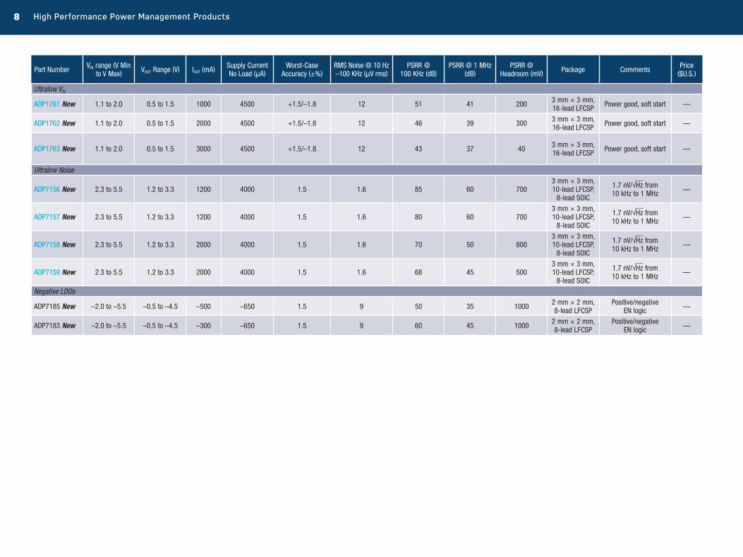
8 High Performance Power Management Products
Part Number VIN range (V Min to V Max) VOUT Range (V) IOUT (mA) Supply Current
No Load (μA)Worst-Case
Accuracy (±%)RMS Noise @ 10 Hz –100 KHz (μV rms)
PSRR @ 100 KHz (dB)
PSRR @ 1 MHz (dB)
PSRR @ Headroom (mV) Package Comments Price
($U.S.)
Ultralow VIN
ADP1761 New 1.1 to 2.0 0.5 to 1.5 1000 4500 +1.5/–1.8 12 51 41 200 3 mm × 3 mm, 16-lead LFCSP Power good, soft start —
ADP1762 New 1.1 to 2.0 0.5 to 1.5 2000 4500 +1.5/–1.8 12 46 39 300 3 mm × 3 mm, 16-lead LFCSP Power good, soft start —
ADP1763 New 1.1 to 2.0 0.5 to 1.5 3000 4500 +1.5/–1.8 12 43 37 40 3 mm × 3 mm, 16-lead LFCSP Power good, soft start —
Ultralow Noise
ADP7156 New 2.3 to 5.5 1.2 to 3.3 1200 4000 1.5 1.6 85 60 7003 mm × 3 mm, 10-lead LFCSP,
8-lead SOIC
1.7 nV/√Hz from 10 kHz to 1 MHz —
ADP7157 New 2.3 to 5.5 1.2 to 3.3 1200 4000 1.5 1.6 80 60 7003 mm × 3 mm, 10-lead LFCSP,
8-lead SOIC
1.7 nV/√Hz from 10 kHz to 1 MHz —
ADP7158 New 2.3 to 5.5 1.2 to 3.3 2000 4000 1.5 1.6 70 50 8003 mm × 3 mm, 10-lead LFCSP,
8-lead SOIC
1.7 nV/√Hz from 10 kHz to 1 MHz —
ADP7159 New 2.3 to 5.5 1.2 to 3.3 2000 4000 1.5 1.6 68 45 5003 mm × 3 mm, 10-lead LFCSP,
8-lead SOIC
1.7 nV/√Hz from 10 kHz to 1 MHz —
Negative LDOs
ADP7185 New –2.0 to –5.5 –0.5 to –4.5 –500 –650 1.5 9 50 35 1000 2 mm × 2 mm, 8-lead LFCSP
Positive/negative EN logic —
ADP7183 New –2.0 to –5.5 –0.5 to –4.5 –300 –650 1.5 9 60 45 1000 2 mm × 2 mm, 8-lead LFCSP
Positive/negative EN logic —
8 High Performance Power Management Products Visit analog.com/power 9
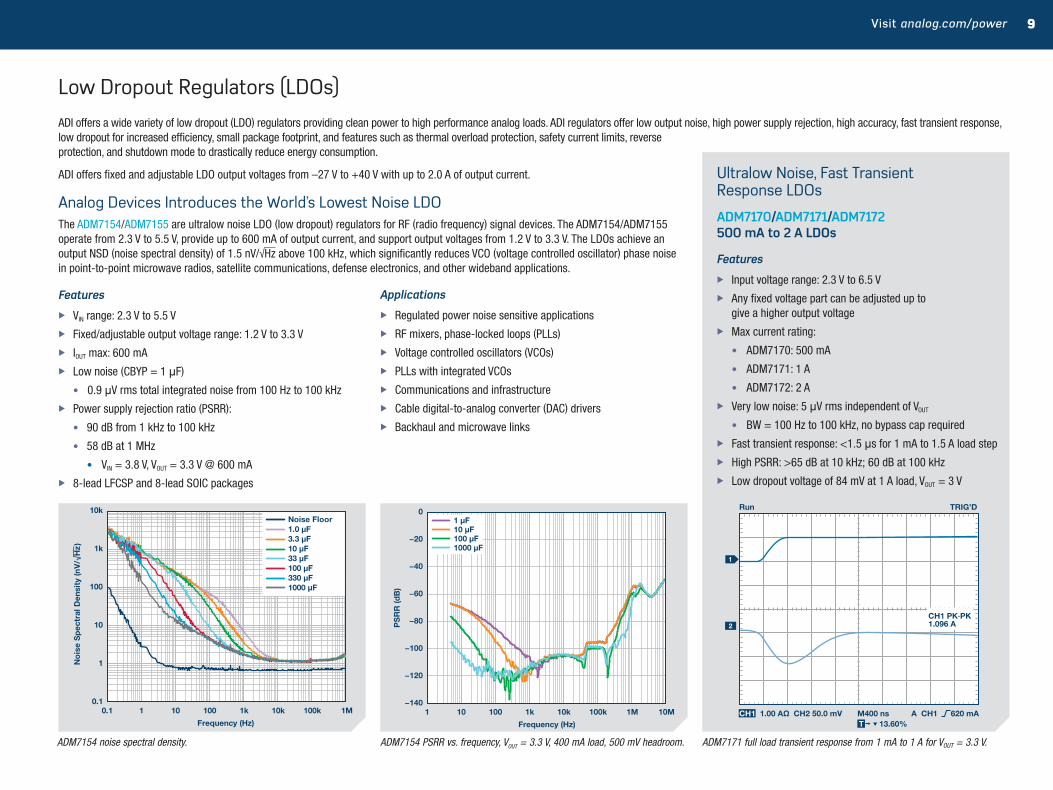
Low Dropout Regulators (LDOs)
ADI offers a wide variety of low dropout (LDO) regulators providing clean power to high performance analog loads. ADI regulators offer low output noise, high power supply rejection, high accuracy, fast transient response, low dropout for increased efficiency, small package footprint, and features such as thermal overload protection, safety current limits, reverse protection, and shutdown mode to drastically reduce energy consumption.
ADI offers fixed and adjustable LDO output voltages from –27 V to +40 V with up to 2.0 A of output current.
Analog Devices Introduces the World’s Lowest Noise LDOThe ADM7154/ADM7155 are ultralow noise LDO (low dropout) regulators for RF (radio frequency) signal devices. The ADM7154/ADM7155 operate from 2.3 V to 5.5 V, provide up to 600 mA of output current, and support output voltages from 1.2 V to 3.3 V. The LDOs achieve an output NSD (noise spectral density) of 1.5 nV/√Hz above 100 kHz, which significantly reduces VCO (voltage controlled oscillator) phase noise in point-to-point microwave radios, satellite communications, defense electronics, and other wideband applications.
PS
RR
(dB
)
Frequency (Hz)
10M1 10 100 1k 10k 100k 1M−140
−120
−100
−80
−60
−40
−20
01 µF10 µF100 µF1000 µF
No
ise
Sp
ectr
al D
ensi
ty (n
V/√
Hz)
Frequency (Hz)
1M0.1 1 10 100 1k 10k 100k0.1
1
10
100
10k
1k
Noise Floor1.0 µF3.3 µF10 µF33 µF100 µF330 µF1000 µF
CH1 1.00 AΩ CH2 50.0 mV M400 ns A CH1 620 mA
Run TRIG’D
2
T 13.60%
1
CH1 PK∙PK1.096 A
Ultralow Noise, Fast Transient Response LDOs
ADM7170/ADM7171/ADM7172 500 mA to 2 A LDOs
Features
X Input voltage range: 2.3 V to 6.5 V
X Any fixed voltage part can be adjusted up to give a higher output voltage
X Max current rating:
• ADM7170: 500 mA
• ADM7171: 1 A
• ADM7172: 2 A
X Very low noise: 5 μV rms independent of VOUT
• BW = 100 Hz to 100 kHz, no bypass cap required
X Fast transient response: <1.5 μs for 1 mA to 1.5 A load step
X High PSRR: >65 dB at 10 kHz; 60 dB at 100 kHz
X Low dropout voltage of 84 mV at 1 A load, VOUT = 3 V
ADM7154 PSRR vs. frequency, VOUT = 3.3 V, 400 mA load, 500 mV headroom.ADM7154 noise spectral density. ADM7171 full load transient response from 1 mA to 1 A for VOUT = 3.3 V.
Features
X VIN range: 2.3 V to 5.5 V
X Fixed/adjustable output voltage range: 1.2 V to 3.3 V
X IOUT max: 600 mA
X Low noise (CBYP = 1 μF)
• 0.9 μV rms total integrated noise from 100 Hz to 100 kHz
X Power supply rejection ratio (PSRR):
• 90 dB from 1 kHz to 100 kHz
• 58 dB at 1 MHz
• VIN = 3.8 V, VOUT = 3.3 V @ 600 mA
X 8-lead LFCSP and 8-lead SOIC packages
Applications
X Regulated power noise sensitive applications
X RF mixers, phase-locked loops (PLLs)
X Voltage controlled oscillators (VCOs)
X PLLs with integrated VCOs
X Communications and infrastructure
X Cable digital-to-analog converter (DAC) drivers
X Backhaul and microwave links
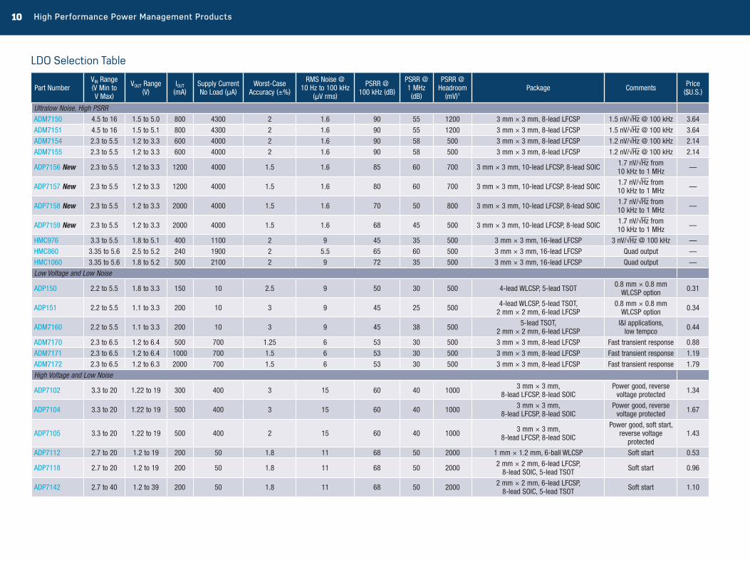
10 High Performance Power Management Products
LDO Selection Table
Part NumberVIN Range (V Min to V Max)
VOUT Range (V)
IOUT (mA)
Supply Current No Load (μA)
Worst-Case Accuracy (±%)
RMS Noise @ 10 Hz to 100 kHz
(μV rms)
PSRR @ 100 kHz (dB)
PSRR @ 1 MHz (dB)
PSRR @ Headroom
(mV)1Package Comments Price
($U.S.)
Ultralow Noise, High PSRRADM7150 4.5 to 16 1.5 to 5.0 800 4300 2 1.6 90 55 1200 3 mm × 3 mm, 8-lead LFCSP 1.5 nV/√Hz @ 100 kHz 3.64
ADM7151 4.5 to 16 1.5 to 5.1 800 4300 2 1.6 90 55 1200 3 mm × 3 mm, 8-lead LFCSP 1.5 nV/√Hz @ 100 kHz 3.64
ADM7154 2.3 to 5.5 1.2 to 3.3 600 4000 2 1.6 90 58 500 3 mm × 3 mm, 8-lead LFCSP 1.2 nV/√Hz @ 100 kHz 2.14
ADM7155 2.3 to 5.5 1.2 to 3.3 600 4000 2 1.6 90 58 500 3 mm × 3 mm, 8-lead LFCSP 1.2 nV/√Hz @ 100 kHz 2.14
ADP7156 New 2.3 to 5.5 1.2 to 3.3 1200 4000 1.5 1.6 85 60 700 3 mm × 3 mm, 10-lead LFCSP, 8-lead SOIC 1.7 nV/√Hz from 10 kHz to 1 MHz —
ADP7157 New 2.3 to 5.5 1.2 to 3.3 1200 4000 1.5 1.6 80 60 700 3 mm × 3 mm, 10-lead LFCSP, 8-lead SOIC 1.7 nV/√Hz from 10 kHz to 1 MHz —
ADP7158 New 2.3 to 5.5 1.2 to 3.3 2000 4000 1.5 1.6 70 50 800 3 mm × 3 mm, 10-lead LFCSP, 8-lead SOIC 1.7 nV/√Hz from 10 kHz to 1 MHz —
ADP7159 New 2.3 to 5.5 1.2 to 3.3 2000 4000 1.5 1.6 68 45 500 3 mm × 3 mm, 10-lead LFCSP, 8-lead SOIC 1.7 nV/√Hz from 10 kHz to 1 MHz —
HMC976 3.3 to 5.5 1.8 to 5.1 400 1100 2 9 45 35 500 3 mm × 3 mm, 16-lead LFCSP 3 nV/√Hz @ 100 kHz —
HMC860 3.35 to 5.6 2.5 to 5.2 240 1900 2 5.5 65 60 500 3 mm × 3 mm, 16-lead LFCSP Quad output —
HMC1060 3.35 to 5.6 1.8 to 5.2 500 2100 2 9 72 35 500 3 mm × 3 mm, 16-lead LFCSP Quad output —
Low Voltage and Low Noise
ADP150 2.2 to 5.5 1.8 to 3.3 150 10 2.5 9 50 30 500 4-lead WLCSP, 5-lead TSOT 0.8 mm × 0.8 mm WLCSP option 0.31
ADP151 2.2 to 5.5 1.1 to 3.3 200 10 3 9 45 25 500 4-lead WLCSP, 5-lead TSOT, 2 mm × 2 mm, 6-lead LFCSP
0.8 mm × 0.8 mm WLCSP option 0.34
ADM7160 2.2 to 5.5 1.1 to 3.3 200 10 3 9 45 38 500 5-lead TSOT, 2 mm × 2 mm, 6-lead LFCSP
I&I applications, low tempco 0.44
ADM7170 2.3 to 6.5 1.2 to 6.4 500 700 1.25 6 53 30 500 3 mm × 3 mm, 8-lead LFCSP Fast transient response 0.88
ADM7171 2.3 to 6.5 1.2 to 6.4 1000 700 1.5 6 53 30 500 3 mm × 3 mm, 8-lead LFCSP Fast transient response 1.19
ADM7172 2.3 to 6.5 1.2 to 6.3 2000 700 1.5 6 53 30 500 3 mm × 3 mm, 8-lead LFCSP Fast transient response 1.79
High Voltage and Low Noise
ADP7102 3.3 to 20 1.22 to 19 300 400 3 15 60 40 1000 3 mm × 3 mm, 8-lead LFCSP, 8-lead SOIC
Power good, reverse voltage protected 1.34
ADP7104 3.3 to 20 1.22 to 19 500 400 3 15 60 40 1000 3 mm × 3 mm, 8-lead LFCSP, 8-lead SOIC
Power good, reverse voltage protected 1.67
ADP7105 3.3 to 20 1.22 to 19 500 400 2 15 60 40 1000 3 mm × 3 mm, 8-lead LFCSP, 8-lead SOIC
Power good, soft start, reverse voltage
protected1.43
ADP7112 2.7 to 20 1.2 to 19 200 50 1.8 11 68 50 2000 1 mm × 1.2 mm, 6-ball WLCSP Soft start 0.53
ADP7118 2.7 to 20 1.2 to 19 200 50 1.8 11 68 50 2000 2 mm × 2 mm, 6-lead LFCSP, 8-lead SOIC, 5-lead TSOT Soft start 0.96
ADP7142 2.7 to 40 1.2 to 39 200 50 1.8 11 68 50 2000 2 mm × 2 mm, 6-lead LFCSP, 8-lead SOIC, 5-lead TSOT Soft start 1.10

10 High Performance Power Management Products Visit analog.com/power 11
Part NumberVIN Range (V Min to V Max)
VOUT Range (V)
IOUT (mA)
Supply Current No Load (μA)
Worst-Case Accuracy (±%)
RMS Noise @ 10 Hz to 100 kHz
(μV rms)
PSRR @ 100 kHz (dB)
PSRR @ 1 MHz (dB)
PSRR @ Headroom
(mV)1Package Comments Price
($U.S.)
Negative Voltage
ADP7182 –2.7 to –28 –1.22 to –27 –200 –33 3 18 45 32 1000
2 mm × 2 mm, 6-lead LFCSP, 3 mm × 3 mm, 8-lead LFCSP,
5-lead TSOT
Positive/negative EN logic 1.29
ADP7185 New –2.0 to –5.5 –0.5 to –4.5 –500 –650 1.5 8 60 45 1000 2 mm × 2 mm, 8-lead LFCSP Positive/negative EN logic —
ADP7183 New –2.0 to –5.5 –0.5 to –4.5 –300 –650 1.5 8 60 45 1000 2 mm × 2 mm, 8-lead LFCSP Positive/negative EN logic —
Ultralow VIN
ADP170 1.6 to 3.6 0.8 to 3.0 300 23 3 30 50 32 500 5-lead TSOT Fixed output 0.33
ADP171 1.6 to 3.6 0.8 to 3.0 300 23 3 30 50 32 500 5-lead TSOT Adjustable output 0.33
ADP172 1.6 to 3.6 0.8 to 3.0 300 23 3 30 50 32 500 4-lead WLCSP 0.95 mm × 0.95 mm WLCSP option 0.33
ADP130 1.2 to 3.6 0.8 to 3.0 350 25 3 29 55 35 500 5-lead TSOT VBIAS voltage required 0.33
ADP1761 New 1.1 to 2.0 0.5 to 1.5 1000 4500 +1.5/–1.8 12 51 41 200 3 mm × 3 mm, 16-lead LFCSP Power good, soft start —
ADP1762 New 1.1 to 2.0 0.5 to 1.5 2000 4500 +1.5/–1.8 12 46 39 300 3 mm × 3 mm, 16-lead LFCSP Power good, soft start —
ADP1763 New 1.1 to 2.0 0.5 to 1.5 3000 4500 +1.5/–1.8 12 43 37 400 3 mm × 3 mm, 16-lead LFCSP Power good, soft start —
ADP1740 1.6 to 3.6 0.75 to 2.5 2000 90 2 23 54 40 1000 4 mm × 4 mm, 16-lead LFCSPSoft start, power
good, reverse voltage protected
1.20
ADP1741 1.6 to 3.6 0.75 to 3.3 2000 90 2 23 54 40 1000 4 mm × 4 mm, 16-lead LFCSPSoft start, power
good, reverse voltage protected
1.20
ADP1752 1.6 to 3.6 0.75 to 2.5 800 90 2 23 54 40 1000 4 mm × 4 mm, 16-lead LFCSPSoft start, power
good, reverse voltage protected
0.90
ADP1753 1.6 to 3.6 0.75 to 3.3 800 90 2 23 54 40 1000 4 mm × 4 mm, 16-lead LFCSPSoft start, power
good, reverse voltage protected
0.90
ADP1754 1.6 to 3.6 0.75 to 2.5 1200 90 2 23 54 40 1000 4 mm × 4 mm, 16-lead LFCSPSoft start, power
good, reverse voltage protected
0.95
ADP1755 1.6 to 3.6 0.75 to 3.3 1200 90 2 23 54 40 1000 4 mm × 4 mm, 16-lead LFCSPSoft start, power
good, reverse voltage protected
0.95

12 High Performance Power Management Products
Part NumberVIN Range (V Min to V Max)
VOUT Range (V)
IOUT (mA)
Supply Current No Load (μA)
Worst-Case Accuracy
(±%)
RMS Noise @ 10 Hz to 100 kHz
(μV rms)
PSRR @ 100 kHz
(dB)
PSRR @ 1 MHz (dB)
PSRR @ Headroom (mV)1 Package Comments Price
($U.S.)
MultirailHMC860LP3E 3.35 to 5.6 2.5 to 5.2 240 1900 2 5.5 65 60 500 3 mm × 3 mm, 16-lead LFCSP Quad output —
HMC1060LP3E 3.35 to 5.6 1.8 to 5.2 500 2100 2 9 72 35 500 3 mm × 3 mm, 16-lead LFCSP Quad output —
ADP220 2.5 to 5.5 0.8 to 3.3 200 60 2 27 60 40 1000 6-lead WLCSP 1 mm × 1.5 mm WLCSP 0.58
ADP221 2.5 to 5.5 0.8 to 3.3 200 60 2 27 60 40 1000 6-lead WLCSP 1 mm × 1.5 mm WLCSP, active pulldown 0.58
ADP222 2.5 to 5.5 0.8 to 3.3 300 65 2 27 60 40 1000 2 mm × 2 mm, 8-lead LFCSP Dual LDO, fixed outputs 0.49
ADP223 2.5 to 5.5 0.5 to 5.0 300 65 2 27 60 40 1000 2 mm × 2 mm, 8-lead LFCSP Dual LDO, adjustable outputs 0.49
ADP224 2.5 to 5.5 0.8 to 3.3 300 65 2 27 60 40 1000 2 mm × 2 mm, 8-lead LFCSP Dual LDO, fixed outputs, quick output discharge 0.49
ADP225 2.5 to 5.5 0.5 to 5.0 300 65 2 27 60 40 1000 2 mm × 2 mm, 8-lead LFCSPDual LDO, adjustable outputs, quick output
discharge0.49
ADP320 1.8 to 5.5 0.8 to 3.3 200 85 2 24 55 45 1000 3 mm × 3 mm, 16-lead LFCSP Triple LDO, 2.5 VBIAS min 0.54
ADP322 1.8 to 5.5 0.8 to 3.3 200 85 2 24 55 45 1000 3 mm × 3 mm, 16-lead LFCSP Triple LDO, 2.5 VBIAS min, fixed outputs 0.54
ADP323 1.8 to 5.5 0.5 to 5.0 200 85 2 24 55 45 1000 3 mm × 3 mm, 16-lead LFCSP Triple LDO, 2.5 VBIAS min, adjustable outputs 0.54
High CurrentADP1762 New 1.1 to 2.0 0.5 to 1.5 2000 4500 +1.5/–1.8 12 46 39 300 3 mm × 3 mm, 16-lead LFCSP Power good, soft start —
ADP1763 New 1.1 to 2.0 0.5 to 1.5 3000 4500 +1.5/–1.8 12 43 37 400 3 mm × 3 mm, 16-lead LFCSP Power good, soft start —
ADM7172 2.3 to 6.5 1.2 to 6.3 2000 700 1.5 6 53 30 500 3 mm × 3 mm, 8-lead LFCSP Fast transient response 1.79
ADP7158 New 2.3 to 5.5 1.2 to 3.3 2000 4000 1.5 1.6 70 50 800 3 mm × 3 mm, 10-lead LFCSP, 8-lead SOIC
1.7 nV/√Hz from 10 kHz to 1 MHz —
ADP7159 New 2.3 to 5.5 1.2 to 3.3 2000 4000 1.5 1.6 68 45 500 3 mm × 3 mm, 10-lead LFCSP, 8-lead SOIC
1.7 nV/√Hz from 10 kHz to 1 MHz —
ADP1740 1.6 to 3.6 0.75 to 2.5 2000 90 2 23 54 40 1000 4 mm × 4 mm, 16-lead LFCSP Soft start, power good,
reverse voltage protected 1.20
ADP1741 1.6 to 3.6 0.75 to 3.3 2000 90 2 23 54 40 1000 4 mm × 4 mm, 16-lead LFCSP Soft start, power good,
reverse voltage protected 1.20
General-Purpose
ADP121 2.3 to 5.5 1.2 to 3.3 150 11 3 40 50 30 1000 5-lead TSOT, 4-lead WLCSP 0.82 mm × 0.82 mm WLCSP 0.27
ADP122 2.3 to 5.5 1.75 to 3.3 300 45 2 25 60 38 500 5-lead TSOT,
2 mm × 2 mm, 6-lead LFCSP Fixed output 0.34
ADP123 2.3 to 5.5 0.8 to 5.0 300 45 2 25 60 38 500 5-lead TSOT, 2 mm × 2 mm, 6-lead LFCSP Adjustable output 0.34
1 PSRR specifications are at this headroom voltage (headroom = VIN – VOUT ).

12 High Performance Power Management Products Visit analog.com/power 13
Part NumberVIN Range (V Min to V Max)
VOUT Range (V)
IOUT (mA)
Supply Current No Load (μA)
Worst-Case Accuracy
(±%)
RMS Noise @ 10 Hz to 100 kHz
(μV rms)
PSRR @ 100 kHz
(dB)
PSRR @ 1 MHz (dB)
PSRR @ Headroom
(mV)1Package Comments Price
($U.S.)
General-Purpose (continued)
ADP124 2.3 to 5.5 1.75 to 3.3 500 45 2 25 45 33 500 8-lead MSOP, 2 mm × 2 mm, 8-lead LFCSP
Exposed pad package for high thermal conductivity 0.42
ADP125 2.3 to 5.5 0.8 to 5.0 500 45 2 25 45 33 500 8-lead MSOP, 2 mm × 2 mm, 8-lead LFCSP
Exposed pad package for high thermal conductivity 0.42
Ultralow IQ and Low NoiseADP160 2.2 to 5.5 1.2 to 4.2 150 0.56 3.5 80 23 20 500 5-lead TSOT, 4-lead WLCSP Ultralow IQ, QOD 0.34
ADP161 2.2 to 5.5 1.0 to 4.2 150 0.56 3.5 80 23 20 500 5-lead TSOT Ultralow IQ 0.34
ADP162 2.2 to 5.5 1.2 to 4.2 150 0.56 3.5 80 23 20 500 5-lead TSOT, 4-lead WLCSPUltralow IQ, QOD,
0.965 mm × 0.965 mm WLCSP0.34
ADP163 2.2 to 5.5 1.0 to 4.2 150 0.56 3.5 80 23 20 500 5-lead TSOT Ultralow IQ 0.34
ADP165 2.2 to 5.5 1.0 to 4.2 150 0.59 3.5 80 23 20 5001 mm × 1 mm, 4-lead WLCSP, 2 mm × 2 mm, 6-lead LFCSP,
5-lead TSOT
Ultralow IQ in dropout (pass through mode), QOD
0.35
ADP166 2.2 to 5.5 1.0 to 4.2 150 0.59 3.5 80 23 20 5001 mm × 1 mm, 4-lead WLCSP, 2 mm × 2 mm, 6-lead LFCSP,
5-lead TSOT
Ultralow IQ in dropout (pass through mode) 0.35
WLCSPADP121 2.3 to 5.5 1.2 to 3.3 150 11 3 40 50 30 1000 5-lead TSOT, 4-lead WLCSP 0.82 mm × 0.82 mm WLCSP 0.27
ADP150 2.2 to 5.5 1.8 to 3.3 150 10 2.5 9 50 30 500 4-lead WLCSP, 5-lead TSOT 0.8 mm × 0.8 mm WLCSP option 0.31
ADP151 2.2 to 5.5 1.1 to 3.3 200 10 3 9 45 25 5004-lead WLCSP, 5-lead TSOT,
2 mm × 2 mm, 6-lead LFCSP0.8 mm × 0.8 mm
WLCSP option 0.34
ADP160 2.2 to 5.5 1.2 to 4.2 150 0.56 3.5 80 23 20 500 5-lead TSOT, 4-lead WLCSP Ultralow IQ, QOD 0.34
ADP162 2.2 to 5.5 1.2 to 4.2 150 0.56 3.5 80 23 20 500 5-lead TSOT, 4-lead WLCSPUltralow IQ, QOD,
0.965 mm × 0.965 mm WLCSP0.34
ADP165 2.2 to 5.5 1.0 to 4.2 150 0.59 3.5 80 23 20 5001 mm × 1 mm, 4-lead WLCSP, 2 mm × 2 mm, 6-lead LFCSP,
5-lead TSOT
Ultralow IQ in dropout (pass through mode), QOD
0.35
ADP166 2.2 to 5.5 1.0 to 4.2 150 0.59 3.5 80 23 20 5001 mm × 1 mm, 4-lead WLCSP, 2 mm × 2 mm, 6-lead LFCSP,
5-lead TSOT
Ultralow IQ in dropout (pass through mode) 0.35
ADP172 1.6 to 3.6 0.8 to 3.0 300 23 3 30 50 32 500 4-lead WLCSP 0.95 mm × 0.95 mm WLCSP option 0.33
ADP220 2.5 to 5.5 0.8 to 3.3 200 60 2 27 60 40 1000 6-lead WLCSP 1 mm × 1.5 mm WLCSP 0.58
ADP221 2.5 to 5.5 0.8 to 3.3 200 60 2 27 60 40 1000 6-lead WLCSP 1 mm × 1.5 mm WLCSP, active pulldown 0.58
ADP7112 2.7 to 20 1.2 to 19 200 50 2 11 60 40 1000 6-lead WLCSP Soft start 0.531 PSRR specifications are at this headroom voltage (headroom = VIN – VOUT
).

14 High Performance Power Management Products Visit analog.com/power 15
Switching Controllers
Switching Controllers That Deliver Highly Efficient and Easy to Use SolutionsAnalog Devices offers a range of versatile, single and dual synchronous switching controllers with external MOSFETs to provide efficient power conversion from a wide input voltage range to output voltages as low as 0.6 V. ADI makes power management design simple by providing easy to use ADIsimPower design software to provide schematics and BOM with a few easy steps. This, added to industry-leading applications support and 50 years of experience in high performance signal processing, makes ADI a reliable and efficient supplier of power management products.
ADI has a very broad range of switching controllers to deliver high current to your point of load. The ADP187x series of wide range input voltage, constant-on-time controllers offers fast transient response with a variety of features depending on the family member selected. The ADP1851 and ADP1853 are wide range input, single-channel, constant frequency controllers. Both devices can be configured as voltage or current mode controllers and can be synchronized to an external clock and provide tracking capability for easy system power-up. The ADP1853 offers the added feature of master clock output.
For higher power levels, the ADP1850 is a flexible, dual-channel or interleaved, current mode controller that offers synchronization, tracking, and simple sequencing capability useful for systems with multiple voltage rails on a card. Similarly, the ADP1829 offers a dual output, volt-age mode controller with synchronization and tracking. ADP1850 demo board 12 VIN to 0.9 V @ 50 A output.
COMP BST
FB
DRVH
GND
SW
VREG
VREG_IN
RES
DRVL
SSCSS
PGND
VIN
CC
CVREG
CVREG2
CC2RC
RBOT
RTOPVOUT
EN10 kΩ
VREG
Q1
Q2
L
COUT
VOUT
CBST
Load
CIN
VIN = 2.95 V to 20 V
ADP1874/ADP1875
RRES
RTRK1
PGOODRPGD
VEXT
TRACKRTRK2
VMASTER
RAMP1
RRAMP1
VIN
DH1BST1
SW1ILIM1
FB1
DL1
PGND1
RAMP2
DH2BST2
SW2ILIM2
FB2
DL2
PGND2
EN1EN2VDL
VCCOTRK1TRK2
SYNC
FREQ
COMP1
COMP2
SS1SS2
AGND
RCSG1
R11
R12
R21
R22
M1
M2
RCSG2
M3L2
L1
VOUT1
VOUT2
VIN
VIN
M4
RRAMP2
PGOOD1PGOOD2
ADP1850
HILO
VIN
M2
M1
FB
SW
PGND
VIN
LDHBST
DLRCSG
RRAMP
RAMP
PGOOD
Sync
TRK
SS
ILIM
EN
COMP
CLKOUT
FREQ
VCCO
VOUT
ADP1853
HI
LO
CS
AGND
VMA
ADP1874/ADP1875: single phase, constant-on-time, single output controllers with tracking and optional power saving mode.
ADP1853: single phase, constant frequency, single output controller. Selectable current or voltage mode with sync, clockout, tracking, and power saving mode.
ADP1850: configured as an interleaved, single output controller with sync, tracking, and power saving mode.

14 High Performance Power Management Products Visit analog.com/power 15
Single Output Switching ControllersPart Number
VIN Range (V) Switching Frequency VOUT Options Architecture Topology
Supply Current Max (Typ) Enable
Power Good
TrackingPower Saving
OptionSync/
ClockoutPackage Comment/Added Features
Price ($U.S.)
ADP1621 2.9 to 5.5 100 kHz to 1.5 MHz Adj Constant frequency, current mode Step-up 1.8 mA • 10-lead MSOP — 1.32
ADP1821 3.7 to 5.5300 kHz to 600 kHz,
sync to 1 MHzAdj Constant frequency, voltage mode Step-down 1 mA • • • 16-lead QSOP — 1.41
ADP1822 3.7 to 5.5300 kHz to 600 kHz,
sync to 1 MHzAdj Constant frequency, voltage mode Step-down 1 mA • • • Sync 24-lead QSOP Margining capability 1.46
ADP1828 3.0 to 20300 kHz to 600 kHz,
sync to 1 MHzAdj Constant frequency, voltage mode Step-down 1.5 mA • • •
Sync/clockout
20-lead QSOP, 20-lead LFCSP
— 1.52
ADP1864 3.15 to 14 580 kHz Adj Constant frequency, current mode Step-down 235 μA 6-lead TSOTNonsynchronous buck;
pin-to-pin compatible with LTC1772, LTC3801
1.06
ADP1870/ADP1871
2.95 to 20300 kHz, 600 kHz,
1 MHzAdj Constant on time, current mode Step-down 1.1 mA • • (ADP1871) 10-lead MSOP,
10-lead LFCSP— 1.08
ADP1872/ADP1873
2.75 to 20300 kHz, 600 kHz,
1 MHzAdj Constant on time, current mode Step-down 1.1 mA • • (ADP1873) 10-lead MSOP
Independent bias supply reduces internal dissipation
1.03
ADP1874/ADP1875
2.95 to 20300 kHz, 600 kHz,
1 MHzAdj Constant on time, current mode Step-down 1.1 mA • • • • (ADP1875) 16-lead QSOP — 1.32
ADP1878/ADP1879
2.95 to 20300 kHz, 600 kHz,
1 MHzAdj Constant on time, current mode Step-down 1.1 mA • • • (ADP1879) 14-lead LFCSP
Low thermal impedance package
1.28
ADP1851/ ADP1853
2.75 to 20 200 kHz to 1.5 MHz AdjConstant frequency,
current/voltage modeStep-down 2.5 mA • • • •
Sync/ clockout
20-lead LFCSPConfigurable as voltage or
current mode controller1.20
ADP1972/ADP1974
6 to 60 50 kHz to 300 KHz Adj Constant frequency, voltage modeStep-up,
step-down1.5 mA •
Sync/ clockout
16-lead TSSOPCompanion to AD8450
for battery systems3.50/4.20
Dual Output and Interleaved ControllersPart Number
VIN Range (V) Switching Frequency VOUT Options Architecture Topology
Supply Current Max (Typ) Enable
Power Good
TrackingPower Saving
OptionSync/
ClockoutPackage Comment/Added Features
Price ($U.S.)
ADP1850 2.75 to 20 200 kHz to 1.5 MHz Dual adj Constant frequency, current mode Step-down 4.5 mA • • • • Sync 32-lead LFCSPConfigurable as interleaved, single output or dual output
1.85
ADP1829 3.0 to 20300 kHz to 600 kHz,
sync to 1 MHzDual adj Constant frequency, voltage mode Step-down 1.5 mA • • • 32-lead LFCSP
Configurable as dual output device
2.13
ADP1876 2.95 to 20 600 kHz Dual adj Constant frequency, current mode Step-down 4.5 mA • • • 32-lead LFCSPAdditional 1.5 VOUT,
150 mA LDO1.89

16 High Performance Power Management Products Visit analog.com/power 17
ADP2370/ADP2371 15 V, 800 mA Switching Regulator
X Ultralow IQ ~14 μA X Required only three external component for
smallest solution size ~53 mm2
X Quick output discharge (ADP2371) X Optional light load efficiency mode X Frequency synchronization X Ideal solution for multicell battery source
ADP2370/ADP2371
FSEL
EN
Power Good
VOUT = 3.3 V
VIN = 6 V
CIN10 µF
COUT10 µF
VIN
SYNC
On
Off
1.2 MHz
600 kHzSW
PG
PGND
FB
1
2
3
4
8
7
6
5
ADP2384/ADP2386 20 V, 4 A/6 A Switching Regulator
X Best-in-class efficiency: >95% X Accurate current limit allows the use of smaller inductor X Power good and precision enable pin for simplified sequencing X Adjustable frequency and frequency sync to avoid
interference in multirail applications X Ideal solution for 12 V and 5 V input rail
ADP2384/ADP2386
BST
FB
COMP
PGOOD
GNDVREG
RT
SYNC
SS
L
CVREG
RT
SW
PGND
EN
PVINCIN
VIN CBST
COUT
VOUT
RTOP
RBOT
CC
RC
CSS
ADP2323/ADP2325 20 V, Dual 3 A/5 A Regulator
X ADP2323: dual 3 A or single 6 A X ADP2325: dual 5 A or single 10 A X Programmable switching frequency X Optional light load efficiency X Ideal solution for 12 V and 5 V input in multirail configuration
INTVCC
RTOP1
CC1
RC1 CSS1
CINT
CDRV
CIN1
CBST1
CBST2
L1
M1
M2
L2
VIN
VIN
VOUT1
COUT1
COUT2
VOUT2
RBOT1
RTOP2
RC2
CC2
CSS2
CIN2
RBOT2
ROSC
FB1
CO
MP
1
SS
1
EN
1
PV
IN1
BS
T1
FB2
CO
MP
2
SS
2
EN
2
PV
IN2
BS
T2
ModeSCFGTRK2TRK1VDRV ADP2323/
ADP2325GND
PGOOD2PGOOD1SYNCRT
SW1
DL1
PGND
DL2
SW2
Switching Regulators
ADI provides a wide range of switching regulators with integrated FETs for step-up (boost), invert, and step-down (buck) applications with fixed and adjustable output voltage options. This highly integrated, versatile family of products is intended to minimize external components for space challenged applications. The switching regulator devices combine with Analog Devices online ADIsim design tools to offer extremely easy to use solutions.

16 High Performance Power Management Products Visit analog.com/power 17
Step-Down (Buck) Low IQPart Number VIN Range (V) VOUT Options (V) IOUT Max (A) Typical IQ (μA) Switching Frequency
(MHz) Package Additional Features Price ($U.S.)
Very High Switching Frequency (≥3 MHz), Ultralow IQ , and Smallest Solution SizeADP2121 2.3 to 5.5 1.80, 1.82, 1.85, 1.875 0.5 36 6 6-ball WLFCSP 0.80
ADP2108 2.3 to 5.5 1.0, 1.1, 1.2, 1.3, 1.5, 1.8, 1.82, 2.3, 2.5, 3.0, 3.3 0.6 19 3 5-ball WLFCSP, 5-lead TSOT 0.60
ADP2109 2.3 to 5.5 1.0, 1.2, 1.5, 1.8 0.6 19 3 5-ball WFCSP Quick output discharge 0.70
ADP2140 2.3 to 5.5 Buck: 1.2 to 3.3, LDO: 1.2 to 3.3 Buck: 0.6, LDO: 0.3 42 3 10-lead LFCSP Independent enable or auto sequencing 1.20
ADP2138 2.3 to 5.5 0.8, 1.0, 1.2, 1.5, 1.8, 2.5, 2.8, 3.0, 3.3 0.8 24 3 6-ball WLFCSP 0.90
ADP2139 2.3 to 5.5 0.8, 1.0, 1.2, 1.5, 1.8, 2.5, 2.8, 3.0, 3.3 0.8 24 3 6-ball WLFCSP Quick output discharge 0.90
ADP2147 2.3 to 5.5 0.9/1.3, 1.2/1.0, 0.9/1.1, 1.275/0.981 0.8 23 3 6-ball WLFCSP Simple dynamic voltage scaling 0.90
Extended Input Range, Ultralow IQ , and Small Solution SizeADP2370 3.2 to 15 1.2, 1.5, 1.8, 2.5, 3.0, 3.3, 5.0, adj (0.8 to VIN ) 0.8 14 0.6/1.2 8-lead LFCSP 1.40
ADP2371 3.2 to 15 1.2, 1.8, 3.3, adj (0.8 to VIN ) 0.8 14 0.6/1.2 8-lead LFCSP Quick output discharge 1.40
Ultralow IQ and Small Solution SizeADP2105 2.7 to 5.5 1.2, 1.5, 1.8, 3.3, adj (0.8 to VIN ) 1 20 1.2 16-lead LFCSP 1.13
ADP2106 2.7 to 5.5 1.2, 1.5, 1.8, 3.3, adj (0.8 to VIN ) 1.5 20 1.2 16-lead LFCSP 1.25
ADP2107 2.7 to 5.5 1.2, 1.5, 1.8, 3.3, adj (0.8 to VIN ) 2 20 1.2 16-lead LFCSP 1.32
Ultralow IQ, Dual-Channel Regulators
ADP2230 2.3 to 6.5 1.2, 1.8, 1.2, 3.3, 1.8, 3.3, adj (0.8 to 6) 0.8 15 2 10-lead WLFCSP Internal compensation, quick output discharge, synchronization 1.53
Invert Part Number VIN Range (V) VOUT Options (V) Switch Current Max (A) Switching Frequency (MHz) Package Price ($U.S.)
ADP5073 New 2.85 to 15 Adj (−0.5 to −39 below VIN) 1.2 1.2/2.4 16-lead LFCSP 1.49
ADP5074 New 2.85 to 15 Adj (−0.5 to −39 below VIN) 2.4 1.2/2.4 16-lead LFCSP 1.75
Step-Up or Down (Buck-Boost)
Part Number VIN Range (V) VOUT Options (V) IOUT Max (A) Typical IQ (μA) Switching Frequency (MHz) Package Price ($U.S.)
ADP2503 2.3 to 5.5 2.8, 3.3, 3.5, 4.2, 4.5, 5.0, adj (2.6 to 5.5) 0.6 38 2.5 10-lead LFCSP 1.30
ADP2504 2.3 to 5.5 2.8, 3.3, 3.5, 4.2, 4.5, 5.0, adj (2.6 to 5.5) 1 38 2.5 10-lead LFCSP 1.30
18 High Performance Power Management Products Visit analog.com/power 19
ADP2441 Ultrahigh Efficiency Conversion
FB
COMP
EN
PG
OO
D
FRE
Q
SS
/TR
KPGND
VIN
SW
BS
T
AG
ND
VC
C
ADP2441
C4
C3
CBST
CIN COUT
RTOP
RFREQ
RCOMP
CCOMP
RBOTTOM
VOUT
VOUT
VINADP5073/ADP5074
PWRGDSW
Slew
CVREF
COUT
–5OUT
GND
VREG
COMP
SS
Sync
D1
CVREG
RC
CC
EN
AVIN12 VINPVIN
VREF
RFTFBCIN
OnOff
0
20
40
60
80
100
10
30
50
70
90
Effi
cien
cy (%
)
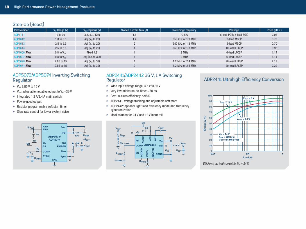
Load (A)
VOUT = 3.3 V
VOUT = 5 V
VOUT = 12 V
VIN = 24 VFSW = 300 kHzCoilcraft MSS1038
0.01 0.1 1
Efficiency vs. load current for VIN = 24 V.
ADP5073/ADP5074 Inverting Switching Regulator
X VIN: 2.85 V to 15 V X VOUT adjustable negative output to VIN –39 V X Integrated 1.2 A/2.4 A main switch X Power-good output X Resistor programmable soft start timer X Slew rate control for lower system noise
ADP2441/ADP2442 36 V, 1 A Switching Regulator
X Wide input voltage range: 4.5 V to 36 V X Very low minimum-on-time: ~50 ns X Best-in-class efficiency: >95% X ADP2441: voltage tracking and adjustable soft start X ADP2442: optional light load efficiency mode and frequency
synchronization X Ideal solution for 24 V and 12 V input rail
Step-Up (Boost) Part Number VIN Range (V) VOUT Options (V) Switch Current Max (A) Switching Frequency Package Price ($U.S.)
ADP1111 2 to 30 3.3, 5.0, 12.0 1.5 70 kHz 8-lead PDIP, 8-lead SOIC 2.06
ADP1612 1.8 to 5.5 Adj (VIN to 20) 1.4 650 kHz or 1.3 MHz 8-lead MSOP 0.78
ADP1613 2.5 to 5.5 Adj (VIN to 20) 2 650 kHz or 1.3 MHz 8-lead MSOP 0.70
ADP1614 2.5 to 5.5 Adj (VIN to 20) 4 650 kHz or 1.3 MHz 10-lead LFCSP 0.95
ADP1606 New 0.8 to VOUT Fixed 1.8 1 2 MHz 6-lead LFCSP 1.14
ADP1607 New 0.8 to VOUT Adj (1.8 to 3.3) 1 2 MHz 6-lead LFCSP 1.14
ADP5070 New 2.85 to 15 Adj (VIN to 39) 1 1.2 MHz or 2.4 MHz 20-lead LFCSP 2.19
ADP5071 New 2.85 to 15 Adj (VIN to 39) 2 1.2 MHz or 2.4 MHz 20-lead LFCSP 2.39

18 High Performance Power Management Products Visit analog.com/power 19
Step-Down (Buck)
Part Number VIN Range (V) VOUT Options (V) IOUT Max
(A)Switching
Frequency (MHz)Power Good
Power Saving Mode
Precision Enable
Voltage Tracking
Frequency Sync
Precharged Output
100% Duty
Operation
Adj Soft Start Package Price
($U.S.)
Fully Integrated FET, High Performance, and Ease of Use
ADP2120 2.3 to 5.5 1.0, 1.2, 1.5, 1.8, 2.5, 3.3, adj (0.6 to VIN )
1.25 1.2 • • • • • • • 10-lead LFCSP 0.94
ADP2119 2.3 to 5.5 1.0, 1.2, 1.5, 1.8, 2.5, 3.3, adj (0.6 to VIN )
2 1.2 • • • • • • • 10-lead LFCSP 1.14
ADP2118 2.3 to 5.5 1.0, 1.2, 1.5, 1.8, 2.5, 3.3, adj (0.6 to VIN )
3 0.6/1.2 • • • • • • • 16-lead LFCSP 1.43
ADP2164 2.7 to 6.5 1.0, 1.2, 1.5, 1.8, 2.5, 3.3, adj (0.6 to VIN )
4 0.6/1.2/adj (0.5 to 1.4) • • • • • • 16-lead LFCSP 1.66
ADP2165 New 2.7 to 5.5 1.0, 1.2, 1.5, 1.8, 2.5, 3.3, adj (0.6 to 0.9 × VIN )
5 Adj (0.25 to 1.4) • • • • • • 24-lead LFCSP 1.73
ADP2166 New 2.7 to 5.5 1.0, 1.2, 1.5, 1.8, 2.5, 3.3, adj (0.6 to 0.9 × VIN )
6 Adj (0.25 to 1.4) • • • • • • 24-lead LFCSP 1.90
ADP2384 4.5 to 20 Adj (0.6 to 0.9 × VIN) 4 Adj (0.2 to 1.4) • • • • • 24-lead LFCSP 1.74
ADP2386 4.5 to 20 Adj (0.6 to 0.9 × VIN ) 6 Adj (0.2 to 1.4) • • • • • 24-lead LFCSP 2.04
ADP2387 New 4.5 to 20 Adj (0.6 to 0.9 × VIN) 6 Adj (0.2 to 1.4) • • • • 24-lead LFCSP 2.04
ADP2389/ADP2390 New 4.5 to 18 Adj (0.6 to 0.9 × VIN) 12 Adj (0.2 to 2.2) • • (ADP2390) • • • 32-lead LFCSP 2.96/3.07
ADP2441 4.5 to 36 Adj (0.6 to 0.9 × VIN ) 1 Adj (0.3 to 1) • • • • • • 12-lead LFCSP 1.78
ADP2442 4.5 to 36 Adj (0.6 to 0.9 × VIN ) 1 Adj (0.3 to 1) • • • • • 12-lead LFCSP 1.83
Dual Output, High Performance, and Highly Configurable
ADP2114 2.75 to 5.5 0.8, 1.2, 1.5, 1.8, 2.5, 3.3, adj (0.6 to VIN )
2 (dual), 4 (single) 0.3/0.6/1.2 • • • • • • • 32-lead LFCSP 1.88
ADP2116 2.75 to 5.5 0.8, 1.2, 1.5, 1.8, 2.5, 3.3, adj (0.6 to VIN )
3 (dual), 6 (single) 0.3/0.6/1.2 • • • • • • • 32-lead LFCSP 2.50
ADP2311 4.5 to 18 Adj (0.6 on both channels) 1 (dual), 1 (single) 0.3 • • • 24-lead LFCSP 2.38
ADP2323 4.5 to 20 Adj (0.6 to 0.9 × VIN )3 (dual), 6 (single) Adj (0.25 to 1.2) • • • • • • • 32-lead LFCSP 2.26
ADP2325 4.5 to 20 Adj (0.6 to 0.9 × VIN )5 (dual),
10 (single) Adj (0.25 to 1.2) • • • • • • • 32-lead LFCSP 2.71
General-Purpose, Leaded Package, and Ease of UseADP2300 3 to 20 Adj (0.8 to 0.85 × VIN ) 1.2 0.7 • • 6-lead TSOT 1.02
ADP2301 3 to 20 Adj (0.8 to 0.85 × VIN ) 1.2 1.4 • • 6-lead TSOT 1.02
ADP2302 3 to 20 2.5, 3.3, 5.0, adj (0.8 to 0.85 × VIN )
2 0.7 • • • 8-lead SOIC 1.12
ADP2303 3 to 20 2.5, 3.3, 5.0, adj (0.8 to 0.85 × VIN )
3 0.7 • • • 8-lead SOIC 1.24
ADP2381 4.5 to 20 Adj (0.6 to 0.9 × VIN ) 6 Adj (0.2 to 1.4) • • • • • 16-lead TSSOP 1.68
ADP3050 3.6 to 30 3.3, 5.0, adj (1.2 to 0.9 × VIN ) 1 0.2 8-lead SOIC 1.81

20 High Performance Power Management Products Visit analog.com/power 21
ADP5054 Powering Xilinx UltraScale FPGAs ADP5070 Powering Bipolar ADC, DAC, Amp, and Mux
Integrated Power Management Solutions (Micro-PMUs)
New Multioutput Regulators Enable Smaller More Reliable Power Solutions for RF/High Speed and Precision Analog Products Along with FPGAs/ProcessorsModern high performance RF/high speed and precision analog products along with FPGAs/processor-based systems require an increasing number of dedicated rails supplying core, I/O, memory, and precision analog voltage rails both positive and negative. Typically, power solutions today make use of standalone switching regulators and LDOs, but board area is shrinking, complicating the task of designing more efficient power management systems. Combining multiple switching regulators and LDOs into a single package enables very small, flexible, highly efficient power management solutions for powering high performance analog and FPGAs/processors with the highest system reliability.
1.0 V
1.8 V
1.5 V
3.3 V
InvertingRegulator
BoostRegulator
ADP5070
6 A Buck
2.5 A Buck
2.5 A Buck
Switch/Mux
Amp/FilterAnalog
Input
ADC
6 A Buck
5 V/12 VADP5054
Xilinx®/Altera®
FPGA
+15 V
–15 V
6 A Buck
2.5 A Buck
2.5 A Buck
6 A Buck
5 V/12 VADP5054
6 A Buck
2.5 A Buck
2.5 A Buck
6 A Buck
ADP5054
Xilinx®
UltraScale™
Kintex/Virtex
VCCINT
VCCAUX
VCCO_1V2
VCCO_1V5
MGTAVCC
MGTAVTT
VCCO_3V3

20 High Performance Power Management Products Visit analog.com/power 21
Integrated Power Management Solutions (Micro-PMUs)
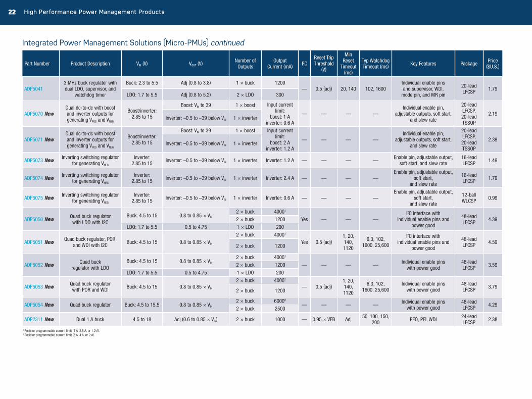
Part Number Product Description VIN (V) VOUT (V) Number of Outputs
Output Current (mA) I2C
Reset Trip Threshold
(V)
Min Reset
Timeout (ms)
Typ Watchdog Timeout (ms) Key Features Package Price
($U.S.)
ADP5022 Dual, 3 MHz buck with 150 mA LDO
Buck: 2.3 to 5.5
Buck: 3.3, 3.0, 2.8, 2.5, 2.3, 2.0, 1.82, 1.8, 1.6, 1.5, 1.3,
1.2, 1.1, 1.0, 0.9, 0.8 2 × buck 600
— — — — Mode pin, individual enable pins
16-ball WLCSP 1.80
LDO: 1.7 to 5.5
LDO: 3.3, 3.0, 2.9, 2.8, 2.775, 2.5, 2.0, 1.875, 1.8, 1.75, 1.7,
1.65, 1.6, 1.55, 1.5, 1.21 × LDO 150
ADP5023 Dual, 800 mA buck with 300 mA LDO
Buck: 2.3 to 5.5 Adj (0.8 to 3.8) 2 × buck 800
— — — — Mode pin, individual enable pins
24-lead LFCSP 1.59
LDO: 1.7 to 5.5 Adj (0.8 to 5.2) 1 × LDO 300
ADP5024 Dual, 1.2 A buck with 300 mA LDO
Buck: 2.3 to 5.5 Adj (0.8 to 3.8) 2 × buck 1200
— — — — Mode pin, individual enable pins
24-lead LFCSP 1.79
LDO: 1.7 to 5.5 Adj (0.8 to 5.2) 1 × LDO 300
ADP5033 Dual, 3 MHz buck regulator with dual LDO
Buck: 2.3 to 5.5
Buck: 3.3, 3.0, 2.8, 2.5, 2.3, 2.0, 1.8,
1.6, 1.5, 1.4, 1.3, 1.2, 1.1, 1.0, 0.9
2 × buck 800
— — — — Mode pin, two enable pins 16-ball WLCSP 1.90
LDO: 1.7 to 5.5
LDO: 3.3, 3.0, 2.8, 2.5, 2.25, 2.0, 1.8,
1.7, 1.6, 1.5, 1.2, 1.1, 1.0, 0.9, 0.8
2 × LDO 300
ADP5034 Dual, 3 MHz buck regulator with dual LDO
Buck: 2.3 to 5.5 Adj (0.8 to 3.8) 2 × buck 1200
— — — — Mode pin, individual enable pins
24-lead LFCSP,
1.99LDO:
1.7 to 5.5 Adj (0.8 to 5.2) 2 × LDO 300 28-lead TSSOP
ADP5133 New Dual, 3 MHz buck regulator Buck: 2.3 to 5.5
Adj (0.8 to 3.8) or 3.3, 3.0, 2.8, 2.5, 2.3, 2.0, 1.8, 1.6, 1.5, 1.4,
1.3, 1.2, 1.1, 1.0, 0.92 × buck 800 — — — — Adjustable and fixed outputs 16-ball
WLCSP 1.29
ADP5134 New Dual, 3 MHz buck regulator with dual LDO
Buck: 2.5 to 5.5 Adj (0.8 to 3.8) 2 × buck 1200
— — — — Precision enable pins and power-good pin
24-lead LFCSP 2.09
LDO: 1.7 to 5.5 Adj (0.8 to 5.2) 2 × LDO 300
ADP5135 New Triple, 3 MHz buck regulator Buck: 3.0 to 5.5 Adj (0.8 to 3.8) 3 × buck 1800 — — — — Precision enable pins
and power-good pins24-lead LFCSP 1.69
ADP5037Dual, 3 MHz, 800 mA
buck regulator with dual 300 mA LDO
Buck: 2.3 to 5.5 Adj (0.8 to 3.8) 2 × buck 800
— — — — Mode pin, individual enable pins
24-lead LFCSP 1.69
LDO: 1.7 to 5.5 Adj (0.8 to 5.2) 2 × LDO 300
ADP5040 3 MHz buck regulator with dual LDO
Buck: 2.3 to 5.5 Adj (0.8 to 3.8) 1 × buck 1200— — — — Individual enable pins,
mode pin20-lead LFCSP 1.39LDO:
1.7 to 5.5 Adj (0.8 to 5.2) 2 × LDO 300
22 High Performance Power Management Products
Part Number Product Description VIN (V) VOUT (V) Number of Outputs
Output Current (mA) I2C
Reset Trip Threshold
(V)
Min Reset
Timeout (ms)
Typ Watchdog Timeout (ms) Key Features Package Price
($U.S.)
ADP50413 MHz buck regulator with dual LDO, supervisor, and
watchdog timer
Buck: 2.3 to 5.5 Adj (0.8 to 3.8) 1 × buck 1200— 0.5 (adj) 20, 140 102, 1600
Individual enable pins and supervisor, WDI,
mode pin, and MR pin
20-lead LFCSP 1.79
LDO: 1.7 to 5.5 Adj (0.8 to 5.2) 2 × LDO 300
ADP5070 NewDual dc-to-dc with boost and inverter outputs for generating VPOS and VNEG
Boost/inverter: 2.85 to 15
Boost: VIN to 39 1 × boost Input current limit:
boost: 1 A inverter: 0.6 A
— — — —Individual enable pin,
adjustable outputs, soft start, and slew rate
20-lead LFCSP, 20-lead TSSOP
2.19Inverter: –0.5 to –39 below VIN 1 × inverter
ADP5071 NewDual dc-to-dc with boost and inverter outputs for generating VPOS and VNEG
Boost/inverter: 2.85 to 15
Boost: VIN to 39 1 × boost Input current limit:
boost: 2 A inverter: 1.2 A
— — — —Individual enable pin,
adjustable outputs, soft start, and slew rate
20-lead LFCSP, 20-lead TSSOP
2.39Inverter: –0.5 to –39 below VIN 1 × inverter
ADP5073 New Inverting switching regulator for generating VNEG
Inverter: 2.85 to 15 Inverter: –0.5 to –39 below VIN 1 × inverter Inverter: 1.2 A — — — — Enable pin, adjustable output,
soft start, and slew rate16-lead LFCSP 1.49
ADP5074 New Inverting switching regulator for generating VNEG
Inverter: 2.85 to 15 Inverter: –0.5 to –39 below VIN 1 × inverter Inverter: 2.4 A — — — —
Enable pin, adjustable output, soft start,
and slew rate
16-lead LFCSP 1.79
ADP5075 New Inverting switching regulator for generating VNEG
Inverter: 2.85 to 15 Inverter: –0.5 to –39 below VIN 1 × inverter Inverter: 0.6 A — — — —
Enable pin, adjustable output, soft start,
and slew rate
12-ball WLCSP 0.99
ADP5050 New Quad buck regulator with LDO with I2C
Buck: 4.5 to 15 0.8 to 0.85 × VIN
2 × buck 40001
Yes — — —I2C interface with
individual enable pins and power good
48-lead LFCSP 4.392 × buck 1200
LDO: 1.7 to 5.5 0.5 to 4.75 1 × LDO 200
ADP5051 New Quad buck regulator, POR, and WDI with I2C Buck: 4.5 to 15 0.8 to 0.85 × VIN
2 × buck 40001
Yes 0.5 (adj)1, 20, 140, 1120
6.3, 102, 1600, 25,600
I2C interface with individual enable pins and
power good
48-lead LFCSP 4.59
2 × buck 1200
ADP5052 New Quad buck regulator with LDO
Buck: 4.5 to 15 0.8 to 0.85 × VIN
2 × buck 40001
— — — — Individual enable pins with power good
48-lead LFCSP 3.592 × buck 1200
LDO: 1.7 to 5.5 0.5 to 4.75 1 × LDO 200
ADP5053 New Quad buck regulator with POR and WDI Buck: 4.5 to 15 0.8 to 0.85 × VIN
2 × buck 40001
— 0.5 (adj)1, 20, 140, 1120
6.3, 102, 1600, 25,600
Individual enable pins with power good
48-lead LFCSP 3.79
2 × buck 1200
ADP5054 New Quad buck regulator Buck: 4.5 to 15.5 0.8 to 0.85 × VIN
2 × buck 60002
— — — — Individual enable pins with power good
48-lead LFCSP 4.29
2 × buck 2500
ADP2311 New Dual 1 A buck 4.5 to 18 Adj (0.6 to 0.85 × VIN) 2 × buck 1000 — 0.95 × VFB Adj 50, 100, 150, 200 PFO, PFI, WDI 24-lead
LFCSP 2.38
1 Resistor programmable current limit (4 A, 2.5 A, or 1.2 A). 2 Resistor programmable current limit (6 A, 4 A, or 2 A).
Integrated Power Management Solutions (Micro-PMUs) continued

22 High Performance Power Management Products Visit analog.com/power 23
Ultralow Power Microenergy Harvesters
Analog Devices offers ultralow power boost regulators for photovoltaic and thermoelectric energy harvesting systems. The ADP5090 delivers efficient conversion of the harvester’s limited power down to the 15 μW to 1 mW range by offering best-in-class sub-μW power conversion losses. The ADP5090’s programmable maximum power point tracking feature ensures that the most energy is extracted from the harvester and the 260 nA quiescent current deep sleep mode prolongs the system’s operational time by minimizing losses in the absence of ambient energy. The integrated charge pump circuit enables cold start down to 380 mV input voltage when no energy is present on the system node.
4.7 µF4.7 µF
6.34 MΩ
14.7 MΩ 10 nF
22 µF
OptionalCR2032
3 V 225 mAh
GaAs Thin FilmAlta Devices
10 MΩADF70xx(Rx/Tx)
MCU(Always-On)
SensorADP160/ADP161
PGOOD
SYS
BAT
REF
PAS409HR0.03 F
3.3 V 12 µAh
SWVIN
MPPT
CBP
BACK_UP
ADP5090
DIS_SW
MINOP
AGND PGND
SETSD
SETPG
TERM
A-SiliconSanyo
Dye-Sensitized Solar CellGCELL; ElectricFilm™
10 nF
Buck TEGMarlow ETEG HV56
4.7 µF4.7 µF
10 MΩ
10 MΩ
22 µF
OPTIONALCR2032
3 V 225 mAh
ADF70xx(Rx/Tx)
MCU(Always-On)
SensorADP160/ADP161
PGOOD
SYS
BAT
REF
PAS409HR0.03 F
3.3 V 12 µAh
SWVIN
MPPT
CBP
BACK_UP
ADP5090
DIS_SW
MINOP
AGND PGND
SETSD
SETPG
TERM
Thin Film TEGLaird ETEG HV56
Photovoltaic Cell/Solar Panel
Thermoelectric Generator
90
0
10
20
30
40
50
0.01E
ffici
ency
Input Current (mA)
0.1 1 10
60
70
80
ADP5090COMP 2COMP 1
ADP5090 Features
X Ultralow power boost regulator
X Hysteretic controller optimizes sub-1 mW efficiency
X Cold start from 16 μW at VIN = 380 mV
X Ultralow quiescent current
X IQ (sys) = 320 nA when VIN (OCV) > MINI_OP
X IQ (sys) = 260 nA when VIN (OCV) < MINI_OP
X OCV (open circuit voltage) sensing maximum power point tracking
X Programmable MPPT ratio for PV or TEG
X Programmable automatic switcher shutdown point (MIN_OP)
X Energy storage management
X Programmable charging termination voltage and shutdown volt-age level to prevent overcharging and overdischarging
X Support optional back-up battery power path (primary cell battery)
X RF transmission friendly
X Ability to shut down switcher temporarily via MCU communication

24 High Performance Power Management Products Visit analog.com/power 25
Ultralow Power Regulators
Analog Devices has introduced a new ultralow power regulator, ADP5310, which consumes extremely low current during regulation and therefore generates superior efficiency, particularly in ultralight load (sub-1 mW) conditions, making it ideal for battery-powered applications in which the system is always on. Unlike switchers that employ traditional PSM (power saving mode) approaches, which still may consume tens of microamps of quiescent current, ADP5310 has a proprietary scheme that consumes only 600 nA IQ, enabling efficient conversion even for loads in the microamp range.
Moreover, ADP5310 is equipped with selectable forced PWM mode, offering a low noise output to power sensitive RF and analog loads making ADP5310 ideal for powering systems that need a low IQ standby mode as well as a low noise active mode.
ULP Micro-PMU for Smart Metering RF Module ULP Micro-PMU for Low Power DSP Companion
ADF70xx(Rx/Tx)
MCI(Always-On)
PowerAmplifier
Always-on
Hibernate
MODE/SYNC
EN3VOUT3
R1R2
From MCU
Mode:High: Forced PWMLow: Forced Hysterectic
From MCU
To MCU
22 µF
1 µF
1 µF
VREG AGND
2.2 V to 2.8 V@ 15 mA
2.2 V to 2.8 V@ 2 µA
2.2 V to 2.8 V@ 400 mA
10 µF
4.7 µH
4.7 µH
10 µF
1 µF
MAX: 15 VMIN: 2.7 V
FB2
PGND2
SW2
FB1
PGND1
SW1
PVIN2
PVIN1
PWRGD
EN1
+
+–
–
CH1 BuckRegulator
800 mA
ADP5310
CH2Ultralow
Power BuckRegulator
50 mA/300 mA
CH3Load Switch
VOUT Control(By DAC or
Switch)
CH1 BuckRegulator
Auto PSM/PWM
800 mA
ADP5310
CH2Ultralow
Power BuckRegulator
50 mA/500 mA
CH3Load Switch
ADP160
ADI LowPowerDSP
(Blackfin)
VDD_EXTVDD_OTP
VDD_HADCVDD_USBVDD_RTC
MODE
EN3VOUT3
R1R2
From DSP
Mode:High: Forced PWMLow: Forced Hysterectic
From DSP
To DSP
22 µF
1 µF
VREG AGND
3.3 V
1.1 V
1.8 V
10 µF
4.7 µH
4.7 µH
10 µF
MAX: 15 VMIN: 2.7 V
FB2
PGND2
SW2
FB1
PGND1
SW1
PVIN2
PVIN1
PWRGD
EN1
+
+–
–
VDD_INT
VDD_DMC
Always-on
Hibernate
VOUT Control(By DAC or
Switch)
In addition to efficient ultralow power conversion, ADP5090 provides excellent system design flexibility. For example, built-in programmability enables the part to handle the charging of different types of energy storage mediums. If an optional backup cell battery is added to the system, ADP5090 will intelligently manage and prioritize the power path via fully integrated power switches. ADP5090 can transition to a quiet, no switching mode within 10 μs to reduce noise during RF transceiver data communication periods.
Part Number Topology Quiescent Current (Standby Current) (nA)
VIN Operating Range
VIN Cold Startup VSYS < 1.8 V
Max Input Current (mA)
Termination Charging Voltage
(V)
Shutdown Discharging Voltage (V)
Accuracy over Temperature Cell Type Package Price1
($U.S.)
ADP5090 New Switching/boost
300 (CBP > MIN_OP) 260 (CBP < MIN_OP) 80 mV to 3.3 V 380 mV 100 mA 2.2 to 5.2 (Adj) 2.0 to VTERM (Adj) 3% SuperCap
Li-Ion3 mm × 3 mm 16-lead LFCSP 1.99
11000 to 4999.

24 High Performance Power Management Products Visit analog.com/power 25
90
0
30
40
50
0.001
Effi
cien
cy
Output Current (mA)
0.01 0.1 1 10 100
60
70
80
ADP5310 CH2ADP2370
Efficiency VIN = 6 V, VOUT = 2.8 V.
Part Number Topology Configuration Quiescent Current (Standby Current) (nA)
VIN Operating Range (V) VOUT Programmable Range (V) Max Output
Current (mA) Special Features Package Price1 ($U.S.)
ADP5300 New Switching (buck) 1 × buck 230 nA (VIN = 4.2 V) 2.05 to 6.5 Adjustable via single resistor
0.8 to 5.0 (32 options) 500Selectable hysteretic or FPWM mode,
optional SYNC clocking, QOD, and voltage monitoring
10-lead LFCSP, 9-ball WLCSP 0.95
ADP5310 New Switching (buck)
2 × buck 1 × load switch
620 nA (VIN = 6.0 V) 690 nA (IIN = 15 V) 2.7 to 15.0
CH1: 1.2, 1.5, 1.8, 2.5, 2.85, 3.3, 5 or adjustable
CH2: 1.2 to 5.0 (50 mV per step) or adjustable
CH1: 800 CH2: 300
Selectable hysteretic or FPWM mode, optional SYNC clocking, and QOD 16-lead TSSOP-EP 1.99
ADP160/ADP161/ADP162/ADP163 New
Linear (LDO) 1 × LDO 560 nA (IOUT = 0 μA) 2.2 to 5.5 Fixed option from 1.2 to 4.2 or adjustable 150 QOD option 5-lead TSOT,
4-ball WLCSP 0.34
ADP165 New Linear (LDO) 1 × LDO 590 nA (IOUT = 0 μA) 2.2 to 5.5 Fixed option from 1.2 to 4.2 or adjustable 150 Pass through mode and QOD 6-lead TSOT, 6-lead
LFCSP, 4-ball WLCSP 0.35
ADP166 New Linear (LDO) 1 × LDO 590 nA (IOUT = 0 μA) 2.2 to 5.5 Fixed option from 1.2 to 4.2 or adjustable 150 Pass through mode, no QOD 6-lead TSOT, 6-lead
LFCSP, 4-ball WLCSP 0.35
11000 to 4999

26 High Performance Power Management Products Visit analog.com/power 27
Digital Power and Drivers
Digital Power for Isolated Power ConversionAnalog Devices leads the market in digital power controllers for ac-to-dc and isolated dc-to-dc power supply systems with award winning products and technology that enable customers to capitalize on the flexibility of digital technology without the pain of complex programming. All digital controllers are complemented by an easy to use graphics user interface (GUI) that enables fast system optimization of efficiency and performance and reduces time to market.
The ADP1046A (W—automotive) is an advanced digital controller with seven PWM logic outputs and is suited to parallel and redundant power supply operation and offers current sharing functions and control of the external OR-FET for redundant power supply applications. The ADP1046A (W) can be used to drive the latest high efficiency LLC resonant mode architectures.
ADP1050/ADP1051/ADP1052 are extremely compact digital controllers with 4 PWM/6 PWM logic outputs capable of controlling most high efficiency power supply topologies with synchronous rectification. All devices have an extensive PMBus™ command set with multiple energy saving modes. The ADP1051/ADP1052 are designed for parallel power supply connection with programmable passive current share, reverse current protection, precharge startup, and conditional overvoltage protection. The ADP1052 adds peak parameter measurements for system power mapping.
The ADP1055 introduces high bandwidth, high switching frequency, and fast transient response to digital power control—approaching analog performance. The ADP1055 adds extensive access and password protection and advanced diagnostics capability, first fault instance detection and Blackbox capability.
All ADP104x/ADP105x advanced digital controllers are supported by evaluation kits and reference designs at: http://www.analog.com/en/power-management/digital-power-management/products/index.html.
Part Number Description Key Features VIN (V) Interface EEPROM PWM Outputs Housekeeping I/O Protection Package Temperature
Range (°C)Price @
1k ($U.S.)
ADP1046A/ADP1046AW
Single-channel digital controller with LLC resonant
mode, current share, and FET-Oring control
LLC resonant mode control, current share, and OR-FET control voltage feedforward 3.3 I2C Yes 7 ACSNS, FLAGIN, PGOOD1,
PGOOD2, PSON
OVP, UVP, OTP, OCP, ACSNS, GND
continuity24-lead QSOP –40 to +85
ambient 3.21
ADP1053 Configurable dual-channel digital controller
Frequency synchronization, voltage feedforward 3.3 I2C/
PMBus Yes 8 ACSNS, PGOOD (2), PSON (2), FLAGIN, FLAGOUT, SYNC OVP, UVP, OCP, OTP (2) 40-lead LFCSP –40 to +125
junction 5.30
ADP1050Single-channel digital controller with PMBus
interface
PMBus interface, synchronization, power saving modes 3.3 I2C/
PMBus Yes 4ACSNS/VF, PGOOD/ALERT,
control/enable, SYNC/FLAGIN
OVP, UVP, OCP, OTP 20-lead LFCSP –40 to +125 junction 3.40
ADP1051/ADP1052
Single-channel digital controller with PMBus
interface
PMBus interface, parallel configurable, synchronization,
power saving, adaptive dead time; ADP1052: peak measurement capability
3.3 I2C/PMBus Yes 6
ACSNS/VF, PGOOD/ALERT, control/enable, SYNC/
FLAGIN
Redundant OVP, UVP, OCP, OTP 24-lead LFCSP –40 to +125
junction 3.90/4.10
ADP1055
Advanced digital controller with PMBus interface with high switching frequency
capability
PMBus interface, high bandwidth, fast transient capability, active clamp snubber, power saving modes and adaptive dead
time, Blackbox diagnostics, and password protection
3.3 I2C/PMBus Yes 6 + 2
ACSNS/VF, PGOOD/ALERT, control/enable, SYNC/
FLAGIN, 4 × GPIO
Redundant OVP, UVP, OCP, OTP 32-lead LFCSP –40 to +125
junction 4.60
Intuitive graphic user programming eliminates complex coding and software qualification.

26 High Performance Power Management Products Visit analog.com/power 27
Digital Power Factor Correction (PFC) with Accurate Input Power Meter
Digital Power Factor Correction Controllers with Accurate Power MeteringPart Number Description Key Features VIN (V) Interface EEPROM PWM Outputs Housekeeping I/O Protection Package Temperature
Range (°C)Price @
1k ($U.S.)
ADP1047 Single phase PFC controller with accurate power metering
Inrush control, real-time efficiency optimization, enhanced dynamic response,
synchronization, spread spectrum3.3 I2C/PMBus Yes 2 PSON, inrush control,
ACOK, PGOOD
Programmable ac fault detection, OCP,
OVP, OTP24-lead QSOP –40 to +85
ambient 3.00
ADP1048/ADP1048W
Interleaved PFC controller with accurate power metering
Inrush control, real-time efficiency optimization, enhanced dynamic response,
synchronization, spread spectrum3.3 I2C/PMBus Yes 2 PSON, inrush control,
ACOK, PGOOD
Programmable ac fault detection, OCP,
OVP, OTP24-lead QSOP –40 to +85
ambient 3.60
High Speed MOSFET Drivers The ADP3654/ADP3634/ADP3624/ADP3630 family of high current, dual, high speed drivers complements the ADI digital power controllers. This family uses an industry-standard driver footprint but adds switching perfor-mance and enhanced reliability. The ADP3634/ADP3624/ADP3630 driver family has two levels of thermal protection (overtemperature warning and shutdown), provides a precision enable that can be used to provide system protection and safety, and includes UVLO to protect the power FET from supply rail droop. The ADP3650 is introduced as a dual MOSFET driver suited to driving nonisolated point-of-load synchronous buck converters.
High Speed Drivers
Part Number Description VIN (V) Peak Drive Current (A)
Propagation Delay Rising
Typ (ns)
UVLO_ON/OFF Threshold Typ (V)
Precision Enable/Shutdown
OT Protection
OT Warning Signal Package
Ambient Temperature Range (°C)
Price @ 1k ($U.S.)
ADP3654 Dual noninverting 4.5 to 18 4 14 4.2, 3.9 No No No 8-lead MSOP_EP, 8-lead SOIC_N_EP
–40 to +125 junction 0.74/0.66
ADP3633/ ADP3634/ ADP3635
Dual inverting (ADP3633), dual noninverting (ADP3634), inverting/
noninverting (ADP3635)9.5 to 18 4 14 8.7, 7.7 Yes Yes Yes 8-lead MSOP_EP,
8-lead SOIC_N_EP –40 to +85 0.96/0.88
ADP3623/ ADP3624/ ADP3625
Dual inverting (ADP3623), dual noninverting (ADP3624), inverting/
noninverting (ADP3625)4.5 to 18 4 14 4.2, 3.9 Yes Yes Yes 8-lead MSOP_EP,
8-lead SOIC_N_EP –40 to +85 0.96/0.88
ADP3629/ ADP3630/ ADP3631
Dual inverting (ADP3629), dual noninverting (ADP3630), inverting/
noninverting (ADP3631)9.5 to 18 2 14 8.7, 7.7 Yes Yes Yes 8-lead MSOP,
8-lead SOIC_N –40 to +85 0.81/0.76
ADP3650 Buck sync rectifier 4.15 to 13.2 — 30 4.15, 3.0 Yes No No 8-lead LFCSP, 8-lead SOIC –40 to +85 0.70/ 0.62
ADP1048 600 W interleaved PFC evaluation kit. 85 VAC to 265 VAC input to 385 VDC output.
The ADP1047 and ADP1048 digital power factor correction controller series offers versatile controllers with power metering capability to ±1% accuracy. The ADP1047 is a single phase device, while the ADP1048 is an interleaved controller and can be configured as a bridgeless PFC for high system efficiency. The PMBus interface
allows parameters to be adjusted and reported including accurate measurement of input voltage, current, and power. The ADP1047/ADP1048 can be programmed using the easy to use graphic user interface, enabling ac-to-dc designers and system architects to optimize efficiency and power system performance.

28 High Performance Power Management Products Visit analog.com/power 29
Positive Hot SwapPart Number Input Range (V) Circuit Breaker Sense Voltage (mV) Input Control Digital Interface Current Sense Accuracy Other Features Package Price1 ($U.S.)
ADM4210 2.7 to 16.5 50 UV/enable — — — 6-lead TSOT 1.99
ADM1170 1.6 to 16.5 50 UV/enable — — SS 8-lead TSOT 2.13
ADM1171 2.7 to 16.5 50 UV/enable — ±5 @ 50 mV (analog) SS, CSOUT 8-lead TSOT 2.23
ADM1172 2.7 to 16.5 50 UV/enable — — PFI, PFO 8-lead TSOT 2.02
ADM1270 4 to 60 50 UV/OV/enable — ±5 @ 50 mV (analog) Adj current limit, power good 16-lead LFPCP, 16-lead QSOP 2.49
1 1000 to 4999
–48 V Hot Swap Controller Part Number Voltage Range (V) Undervoltage Detection/Overvoltage Detection Digital V and I Readback Additional Features Package Price1 ($U.S.)
ADM1070 Shunt regulated UV pin, OV pin — — 6-lead SOT-23 1.57
ADM1073 Shunt regulated UV pin, OV pin — Soft start, drain pin monitoring, additional I/Os 14-lead TSSOP 2.13
ADM1075 New Shunt regulated UVH pin, UVL pin, OV pin PMBus interface with four addresses; also power readback
Soft start, constant power foldback, fast gate shutdown, adj current sense limit
28-lead LFCSP, 28-lead TSSOP 4.99
1 1000 to 4999.
Hot Swap
Hot Swap ICs with Precision ADCs Deliver Greater Accuracy for Improved Energy SavingsWith industry-leading power monitoring accuracy, hot swap controllers from ADI enable increased energy savings opportunities for communications infrastructure installations. Combined with FET health detection features they ensure a robust and dependable solution.
Low Voltage Positive Hot Swap Controllers with Integrated Power Monitor
X ±0.3% current monitoring accuracy X FET health detection
X Constant power foldback
–48 V Hot Swap Controllers with Integrated Power Monitor
X Constant power foldback for FET SOA protection X Precision (<1.0%) current and voltage measurement
X 25 mV/50 mV full-scale sense voltage
Power Monitors X I2C interface
X Processor interrupt pin
Central O
ffice
Backplane –48 V
–48 V
–48 V RTN
RDROP
RSENSE
N-ChannelMosfet
High AccuracyLinear Inrush
Current Control
IsolatedDC-to-DCConverter
5 V3.3 VGND
ADM1075VIN
Timer
UVLUVH
OVGate
Sense+
PMBus
Sense–
PowerMonitor
VEE
ADM1278
Hot Swap Card
+V
GND
PMBus/I2C Bus
PowerMonitoring
250 W
RSENSEVIN
ControllerADM1293
SDASCLUV
ALERT
CLRB
Watts
CLOAD
Power VoltageEnergy Current Voltage
µP

28 High Performance Power Management Products Visit analog.com/power 29
Low Voltage Positive Hot Swap and Power Monitors
Part NumberInput
Range (V)
Circuit Breaker Sense Voltage (mV)
Input Control Digital Interface Current Sense
Accuracy Other Features Package Price1 ($U.S.)
ADM1175 3.15 to 16.5 100 UV/
enable I2C with 4 addresses ±1.95 @ 100 mV CONV 10-lead MSOP 2.53
ADM1176 3.15 to 16.5 100 UV/
enableI2C with 16 addresses
±1.95 @ 100 mV — 10-lead MSOP 2.53
ADM1177 3.15 to 16.5 100 UV/
enable I2C with 4 addresses ±1.95 @ 100 mV SS 10-lead MSOP 2.53
ADM1178 3.15 to 16.5 100 UV/
enable I2C with 4 addresses ±1.95 @ 100 mV — 10-lead MSOP 2.73
ADM1275 2.95 to 20 5 to 25 UV/OV/
enable
PMBus with 4 addresses,
readback V, I±1 @ 20 mV Foldback, GPO (×2) 5 mm × 5 mm,
20-lead LFCSP 4.49
ADM1276 2.95 to 20 5 to 25 UV/OV/
enable
PMBus with 4 addresses,
readback V, I, P, E±1 @ 20 mV Foldback, GPO (×2),
PWRGD, energy meter5 mm × 5 mm, 20-lead LFCSP 5.29
ADM1278 New 2.0 to 20 5 to 25 UV/OV/enable
PMBus with 4 addresses,
readback V, I, P, E, T±0.3 @ 20 mV
Power foldback, GPO (×2), FET fault, PWRGD, startup limit, SPI, CSOUT,
temperature, energy meter
5 mm × 5 mm, 32-lead LFCSP 2.89
1 1000 to 4999.
Current Sense Amplifiers—High Side
Part Number CM Range (V) Gain Max Sense Voltage (mV)
Operating Range (V) Accuracy Typ (∙%) Package Price1 ($U.S.)
ADM4073T 2 to 28 20 150 3 to 28 1 6-lead SOT-23 0.99
ADM4073F 2 to 28 50 150 3 to 28 1 6-lead SOT-23 0.99
ADM4073H 2 to 28 100 150 3 to 28 1 6-lead SOT-23 0.99
1 1000 to 4999.
Digital Power Monitors
Part Number Operating Range (V)
Current Control Accuracy (∙%)
Worst-Case Current Monitoring Accuracy (%)
Bidirectional Current
Monitoring
ADC Conversion Input CONV
CLR Input
Alert Output
Readback Type
Peak Value
Recording
Energy Meter
Communications Interface Package Price1
($U.S.)
ADM1191 3.15 to 26 105 1.45 @ 75 mV — Yes — Yes V and I — — I2C interface with 4 addresses 10-lead MSSOP 1.92
ADM1192 3.15 to 26 105 1.45 @ 75 mV — — Yes Yes V and I — — I2C interface with 16 addresses 10-lead MSSOP 1.92
ADM1293A New 2.95 to 20 ±25, ±50, ±100, ±200 0.33 @ 20 mV Yes Yes — Yes V, I, P, E Yes Yes PMBus interface
with 16 addresses 16-lead,
4 mm × 4 mm LFCSP 4.19
ADM1293B New 2.95 to 20 ±25, ±50, ±100, ±200 0.75 @ 20 mV Yes Yes — Yes V, I, P, E Yes Yes PMBus interface
with 16 addresses 16-lead,
4 mm × 4 mm LFCSP 2.79
ADM1294A New 2.95 to shunt ±25, ±50, ±100, ±200 0.33 @ 20 mV Yes Yes — Yes V, I, P, E Yes Yes PMBus interface
with 16 addresses 16-lead,
4 mm × 4 mm LFCSP 4.49
ADM1294B New 2.95 to shunt ±25, ±50, ±100, ±200 0.75 @ 20 mV Yes Yes — Yes V, I, P, E Yes Yes PMBus interface
with 16 addresses 16-lead,
4 mm × 4 mm LFCSP 2.99
1 1000 to 4999.
VIN = 5 V
GND Long
VOUT = 5 V
VCC
RSENSE0.01 Ω Q1
CTIMER0.22 µF
CTIMER
Gate
Long
1.3 V
Short
Sense
GateDrive/Logic
On
Timer
ADM4210GND
GND
RON120 kΩ
RG100 Ω
RC100 Ω
CC0.01 µFRON2
10 kΩ
CLOAD470 µF
+
Low voltage positive hot swap controller.
Current sense amplifier.
SENSEP
VAUX
SENSEN
Mux
PMBus and LogicAddressDecoder
LDOInternalSupply
ADM1293
SDAISCLADR1 GNDADR2 SDAO
GPO1/ALERT1/CONV
GPO2/ALERT2
VINRangeSelect ADC
EN
VCC
VCAP

30 High Performance Power Management Products Visit analog.com/power 31
ADP198 6 V, Reverse Protected Load Switch X Low RDSON of 50 mΩ @ VIN = 3.3 V and ILOAD = 200 mA in WLCSP
X Wide input voltage range down to 1.65 V
X IGND = 2.5 μA with IOUT = 0 mA, VIN = 2.8 V
X 5 μA reverse current, VOUT = 6.2 V
X Low shutdown current: 100 nA
X Ultrasmall size WLCSP: 4 bump, 0.5 mm pitch
X Compact 2 mm × 2 mm, 8-lead LFCSP
X Programmable start-up time: 30 μs, 200 μs, 450 μs, 1000 μs
ADP1290 12 V, 2 A, Logic Controlled, High-Side Power Switch X Low RDSON of 40 mΩ X Wide input voltage range: 2.3 V to 13.2 V
X 2 A continuous operating current, TJ < 85°C
X 1.2 V logic compatible enable input
X Low 12 μA quiescent current, VIN = 3.3 V
X Low 12 μA quiescent current, VIN = 3.3 V
X Ultralow shutdown current: 2.0 μA at VIN = 6.5 V
X Ultrasmall 1.0 mm × 1.5 mm, 6-ball, 0.5 mm pitch WLCSP
Load Switches
Controlling power supplies in today’s systems is becoming increasing complex, and ADI’s family of load switches provide a simple way to keep them all under control.
GND
EN
Load
VIN
SEL0
SEL1
VOUT
VIN VOUT
ADP198
SlewRate Control
Level ShiftOffOn
ReversePolarity
Protection
+GND
EN Load
VIN VOUT
ADP1290
ChargePumpOff
On
+–
VIN
VIN In
In
ChargePump
DC
OverTemperature
Control
GND
Reverse CurrentBlock
Out
VIN
EN GND
VOUTCIN 1 µf
1.8 V
ADP198
Load
1 mm × 1 mm, 4-Ball WLCSP 2 mm × 2 mm, 8-Lead LFCSP
1VOUT
2VOUT
3GND
4SEL1
8 VIN
7 VIN
6 EN
5 SEL0
ADP198

30 High Performance Power Management Products Visit analog.com/power 31
Load Switches
Part Number VIN Min (V) ID Max (A) ID Limit (A)
Temperature Protect (°C) Switch RDSON
ISUPPLY @ Shutdown Typ (μA) IGND (μA) Enable Logic (V) Output tON Delay (ms) Features Package Price1
($U.S.)
ADP1190A 1.4 to 3.6 500 — — 0.065 Ω @ 3.6 V 700 nA — 1.2 min — Quad switch 1.2 mm × 1.6 mm 0.60
ADP1196 New 0 to 5.5 3 — 125 0.01 Ω @ 1.8 to 5.5 V 0.25 40 1.2 min 2 0 V switch 1.0 mm × 1.5 mm 0.50
ADP196 1.8 to 5.5 3 4 125 0.01 Ω @ 1.8 to 5.5 V 0.25 40 1.2 to 6 2 — 1.0 mm × 1.5 mm 0.50
ADP196-22/ADP196-23/ADP196-32/ADP196-33
1.8 to 5.5 3 4 125 0.01 Ω @ 1.8 to 5.5 V 0.25 40 1.2 to 6 2 Fault, EN, latch off, retry 1.0 mm × 1.5 mm 0.50
ADP1190 New 1.4 to 3.5 500 mA — — 0.120 Ω @ 1.8V 2 2 1.2 to 3.3 5 Quad switch 1.2 mm × 1.6 mm 0.60
ADP199 0.9 to 3.6 0.5 — — 0.04 Ω @ 1.1 to 3.6 V 0.9 6 1.1 to 3.6 0.02 — 0.8 mm × 0.8 mm 0.32
ADP198 New 1.65 to 6.5 1 — — 0.120 Ω @ 1.8 V 1.1 2.5 1.2 to 6 0.11 Reverse current
protection 1.0 mm × 1.0 mm 0.35
ADP194 1.1 to 3.6 500 mA — — 0.08 Ω @ 1.8 V 0.7 1 1.2 to 3.3 0.007 Reverse current protection 0.8 mm × 0.8 mm 0.32
ADP197 1.8 to 5.5 3 — 125 0.012 Ω @ 1.8 to 5.5 V 18 1 1.2 to 3.3 1 — 1.0 mm × 1.5 mm 0.46
ADP195 1.1 to 3.6 1.1 — — 0.095 Ω @ 1.8 V 5 10 1.2 to 3.3 0.005 — 1.0 mm × 1.0 mm 0.35
ADP191 1.1 to 3.6 500 mA — — 0.105 Ω @ 1.8 V 2 2 1.2 to 3.3 0.005 Active discharge 0.8 mm × 0.8 mm 0.32
ADP190 1.1 to 3.6 500 mA — — 0.105 Ω @ 1.8 V 2 2 1.2 to 3.3 0.005 — 0.8 mm × 0.8 mm 0.32
ADP1290 New 2.3 to 13.2 2 — — 0.04 Ω @ 2.3 V — — — — — 1.0 mm × 1.5 mm 0.88
1 1000 to 4999.
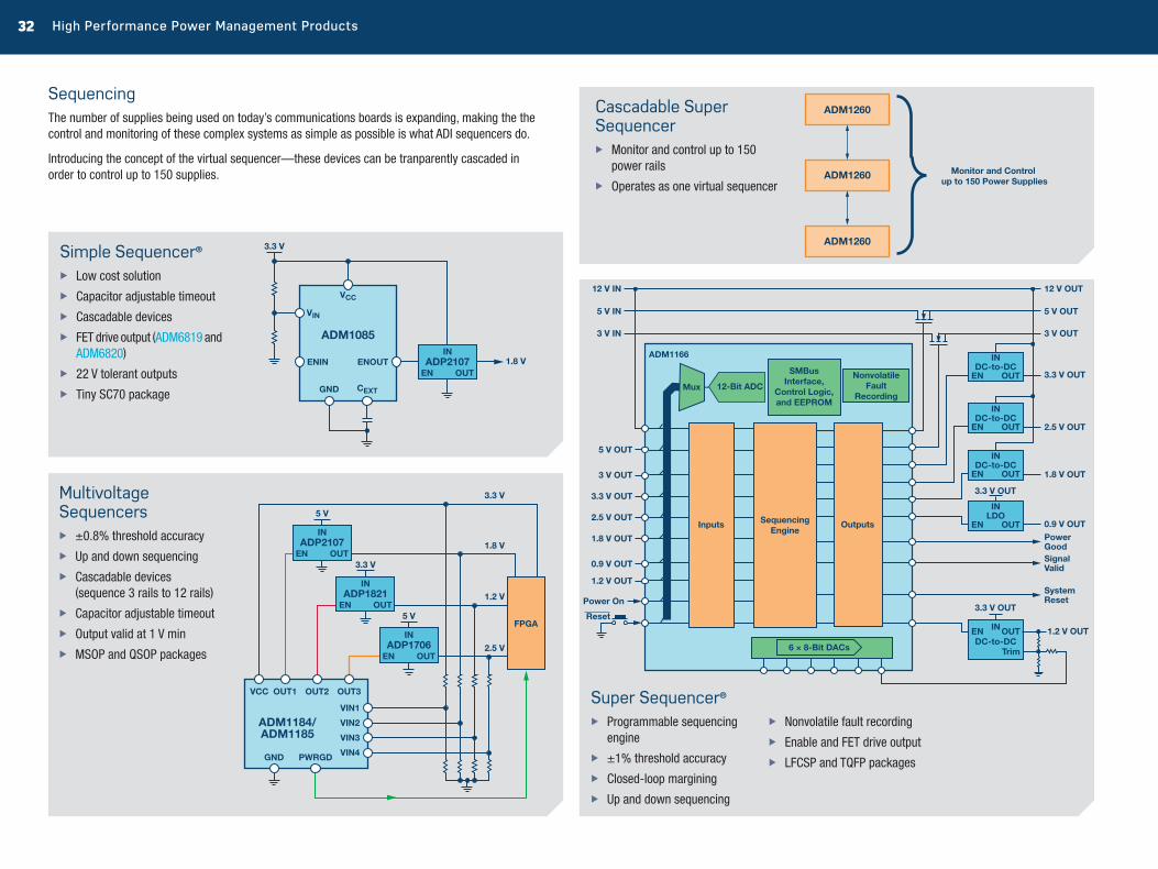
32 High Performance Power Management Products Visit analog.com/power 33
Inputs
5 V OUT
3 V OUT
3.3 V OUT
12 V IN
5 V IN
3 V IN
12 V OUT
5 V OUT
3 V OUT
3.3 V OUT
2.5 V OUT
2.5 V OUT
1.8 V OUT
0.9 V OUT
1.2 V OUT
SequencingEngine
Outputs
ADM1166
12-Bit ADCMux
SMBusInterface,
Control Logic,and EEPROM
NonvolatileFault
Recording
6 × 8-Bit DACs
Power On
Reset
3.3 V OUT
1.8 V OUT
0.9 V OUTPowerGoodSignalValid
SystemReset
1.2 V OUT
IN
EN OUTDC-to-DC
IN
EN OUTDC-to-DC
IN
EN OUTDC-to-DC
IN
EN OUTLDO
3.3 V OUT
INEN OUT
TrimDC-to-DC
3.3 V
1.8 V
1.2 V
2.5 V
IN
5 V
ADP2107EN OUT
IN
3.3 V
ADP1821EN OUT
IN
5 V
ADP1706EN OUT
FPGA
VCC OUT1 OUT2 OUT3
ADM1184/ADM1185
VIN1
VIN2
VIN3
VIN4GND PWRGD
CEXT
VCC
GND
VIN
3.3 V
ENOUTENIN 1.8 VIN
ADP2107
ADM1085
EN OUT
Monitor and Control up to 150 Power Supplies
ADM1260
ADM1260
ADM1260Simple Sequencer®
X Low cost solution
X Capacitor adjustable timeout
X Cascadable devices
X FET drive output (ADM6819 and ADM6820)
X 22 V tolerant outputs
X Tiny SC70 package
Multivoltage Sequencers
X ±0.8% threshold accuracy
X Up and down sequencing
X Cascadable devices (sequence 3 rails to 12 rails)
X Capacitor adjustable timeout
X Output valid at 1 V min
X MSOP and QSOP packages
Cascadable Super Sequencer
X Monitor and control up to 150 power rails
X Operates as one virtual sequencer
Super Sequencer®
X Programmable sequencing engine
X ±1% threshold accuracy
X Closed-loop margining
X Up and down sequencing
X Nonvolatile fault recording
X Enable and FET drive output
X LFCSP and TQFP packages
SequencingThe number of supplies being used on today’s communications boards is expanding, making the the control and monitoring of these complex systems as simple as possible is what ADI sequencers do.
Introducing the concept of the virtual sequencer—these devices can be tranparently cascaded in order to control up to 150 supplies.

32 High Performance Power Management Products Visit analog.com/power 33
Analog Sequencers
Part Number Number of Supplies Monitored
Voltage Monitoring Accuracy (±%)
Number of Output Drivers
FET Drive/Enable Output
Sequencing Package Price ($U.S.)
ADM1085 1: cascadable 7 1 Enable Up 6-lead SC70 0.34
ADM1086 1: cascadable 8 1 Enable Up 6-lead SC70 0.34
ADM1087 1: cascadable 8 1 Enable Up 6-lead SC70 0.34
ADM1184 4: cascadable 0.8 4 Enable Up 10-lead MSOP 1.79
ADM1185 4: cascadable 0.8 4 Enable Up 10-lead MSOP 1.21
ADM1186-1 4: cascadable 0.8 4 Enable Up and down 20-lead QSOP 1.99
ADM1186-2 4 0.8 4 Enable Up and down 16-lead QSOP 1.49
ADM6819 2: cascadable 2.6 1 FET drive Up 6-lead SOT-23 1.21
ADM6820 2: cascadable 2.6 1 FET drive Up 6-lead SOT-23 1.21
Digital Sequencers
Part NumberNumber of Supplies
Monitored
Voltage Monitoring Accuracy
(±%)
Number of Output Drivers
Programming Method
FET Drive/Enable Output
Voltage Readback
Supply Adj/
MarginingPackage Price
($U.S.)
ADM1060 7 2.5 9 SMBus Both — — 6-lead SC70 6.58
ADM1062 10 1 10 SMBus Both 12-bit ADC
12-bit ADC,
6 DACs
40-lead LFSCP, 48-lead TQFP 7.59
ADM1063 10 1 10 SMBus Both 12-bit ADC — 40-lead LFSCP,
48-lead TQFP 8.35
ADM1064 10 1 10 SMBus Both 12-bit ADC — 40-lead LFSCP,
48-lead TQFP 7.84
ADM1065 10 1 10 SMBus Both — — 40-lead LFSCP, 48-lead TQFP 5.82
ADM1066 12 1 10 SMBus Both 12-bit ADC
12-bit ADC,
6 DACs
40-lead LFSCP, 48-lead TQFP 8.60
ADM1067 10 1 10 SMBus Both — 6 DACs 40-lead LFSCP, 48-lead TQFP 6.58
ADM1068 8 1 8 SMBus Both — — 32-lead LQFP 4.05
ADM1069 8 1 8 SMBus Both 12-bit ADC
12-bit ADC,
4 DACs
32-lead LQFP, 40-lead LFSCP 4.40
ADM1166 12 1 10 SMBus Both 12-bit ADC
12-bit ADC,
6 DACs
40-lead LFSCP, 48-lead TQFP 9.99
ADM1168 8 1 8 SMBus Both — — 32-lead LQFP 5.49
ADM1169 8 1 8 SMBus Both 12-bit ADC
12-bit ADC,
6 DACs
32-lead LQFP, 40-lead LFSCP 6.49
ADM1260 New 10: cascadable 1 10 SMBus Both — 6 DACs 40-lead LFSCP 12.99
PWRGND Output
SEQ_DONE Output
Up/Down Input
Time
Voltage 3.3 V
1.2 V
1.8 V
2.5 V
5 V
IN
EN OUTADP1706
5 V
IN
EN OUTADP2107
3.3 V AUX
IN
EN OUTADP1821
5 V
IN
EN OUTADP1706
FAULT
Up
Down
DLY_EN_OUT1
DLY_EN_OUT2
DLY_EN_OUT3
DLY_EN_OUT4
BLANK_DLY
PWRGD
SEQ_DONE
VIN1VIN2VIN3VIN4
VCC OUT1 OUT2
GND
OUT3 OUT4
ADM1186-1
2.5 V
1.8 V
1.2 V
3.3 V
SequenceControl
3.3 V AUX
Power-Up and Power-Down Sequencing with the ADM1186
ADM1186 Power-Up and Power-Down Timing Diagram

34 High Performance Power Management Products Visit analog.com/power 35
Dual
ADM6305: dual supervisor in 5-lead SOT-23.
ADM13305: ±0.8% accurate dual processor supervisor in 8-lead, narrow-body SOIC package.
ADM13307: ±0.8% accurate triple processor supervisor in 8-lead, narrow-body SOIC package.
ADM8614: ultralow power (ICC = 190 nA, max) supervisory ICs with watchdog timer and manual reset.
ADM6710: ±1.5% accurate triple/quad voltage microprocessor supervisor in 6-lead SOT-23 package.
ADM1184: ±0.8% accurate quad voltage monitor in 10-lead MSOP package.
ADM706: voltage monitoring microprocessor supervisory circuits.
Supervisory
Industry’s Lowest Power SupervisorsAs the world goes more portable, quiescent current and a small package are becoming more important. Drawing only 125 nA over temperature and available in tiny WLCSP packaging, ADI supervisory products, such as the new ADM8611/ADM8612 and ADM8641/ADM8642, are ideal for portable applications.
Best Threshold Accuracy: Two Supplies to 12 SuppliesHigh accuracy is critical when monitoring low voltage cores. With up to 2× the accuracy over temperature of competitive parts, these ADI products offer the ability to maintain a much tighter voltage tolerance, thereby maximizing system protection.
Triple QuadQuad
SENSE1
SENSE2
VDD
WDI
Reset FPGA,Micro-
processor,DSP, or
ASIC
VoltageRails ForMonitoring
ADM6305
VIN1 OUT1
VIN2 OUT2
VIN3 OUT3
VIN4 PWRGD
InternalLogic
ADM1184
0.60 V REF
FourVoltage
Rails
ADM6710VIN1
VIN2
VIN3
VIN4
Logic
0.62V VREF
FourVoltage
Rails
Reset
VCC, IN2
FPGAADM13307
FPGA Core Voltage
MR
SENSE1
SENSE2
I/O Supply
VDD
SENSE3
I/O Supply
ResetFPGA
SENSE1
SENSE2
VDD
WDI
ResetFPGA,Micro-
processor,DSP, or
ASIC
VoltageRails ForMonitoring
MR
ADM13305
ADM8614
VCC
MR
Reset
WDI
VTHVCC
WDI
140 ms1.6 s
140 msReset
Micro-processor Reset
GNDMR
PFI
WDI
PFO
ResetVCC
VCC
3.3 V
WDO
5 V
I/O Line
Interrupt
NMI
Manual Reset
GND
GNDVIN VOUT
ADP121
Microprocessor
ADM706R/ADM706S/ADM706T
X 125 nA max supply current
X Reset thresholds from 1.8 V to 4.63 V
X Watchdog timers X WLCSP packaging

34 High Performance Power Management Products Visit analog.com/power 35
Supervisory—Simple Reset/Power-On Reset
Part Number Reset Threshold (V) Min Reset Timeout (ms)
Reset Output Stage Manual Reset Capability
Supply Current Typ (μA) Package Price1
($U.S.)Active Low Active High
ADM1810 4.35, 4.62 100 Push-pull — No 4 3-lead SC70, 3-lead SOT-23 0.45
ADM1811 4.35, 4.62 100 Internal pull-up — No 4 3-lead SC70, 3-lead SOT-23 0.45
ADM1812 4.35, 4.62 100 — Push-pull No 4 3-lead SC70, 3-lead SOT-23 0.45
ADM1813 4.35, 4.62 100 Internal pull-up — Yes 4 3-lead SC70, 3-lead SOT-23 0.39
ADM1815 2.18, 2.31, 2.55, 2.88, 3.06 100 Push-pull — No 4 3-lead SC70, 3-lead SOT-23 0.39
ADM1816 2.18, 2.31, 2.55, 2.88, 3.06 100 Internal pull-up — No 4 3-lead SC70, 3-lead SOT-23 0.45
ADM1817 2.18, 2.31, 2.55, 2.88, 3.06 100 — Push-pull No 4 3-lead SC70, 3-lead SOT-23 0.45
ADM1818 2.18, 2.31, 2.55, 2.88, 3.06 100 Internal pull-up — Yes 4 3-lead SC70, 3-lead SOT-23 0.45
ADM6315 2.63, 2.93, 3.08, 4.39, 4.5, 4.63 1, 20, 140, 1120 Open-drain — Yes 4 4-lead SOT-143 0.73
ADM6319 2.5, 2.63, 2.7, 2.8, 2.93, 3.0, 3.08, 3.2, 3.3, 3.4, 3.5, 3.6, 3.7, 3.8, 3.9, 4.0, 4.1, 4.2, 4.3, 4.39, 4.5, 4.63, 4.7, 4.8, 4.9, 5.0 1, 20, 140, 1120 Push-pull Push-pull Yes 5 5-lead SOT-23 0.50
ADM6322 2.5, 2.63, 2.7, 2.8, 2.93, 3.0, 3.08, 3.2, 3.3, 3.4, 3.5, 3.6, 3.7, 3.8, 3.9, 4.0, 4.1, 4.2, 4.3, 4.39, 4.5, 4.63, 4.7, 4.8, 4.9, 5.0 1, 20, 140, 1120 Open-drain Push-pull Yes 5 5-lead SOT-23 0.50
ADM6326 2.2, 2.32, 2.4, 2.5, 2.63, 2.7, 2.8, 2.93, 3.0, 3.08 100 Push-pull — No 0.5 3-lead SOT-23 0.95
ADM6328 2.2, 2.32, 2.4, 2.5, 2.63, 2.7, 2.8, 2.93, 3.0, 3.08 100 Open-drain — No 0.5 3-lead SOT-23 0.95
ADM6346 3.3, 3.4, 3.5, 3.6, 3.7, 3.8, 3.9, 4.0, 4.1, 4.2, 4.3, 4.38, 4.5, 4.63 100 Push-pull — No 1 3-lead SOT-23 0.95
ADM6348 3.3, 3.4, 3.5, 3.6, 3.7, 3.8, 3.9, 4.0, 4.1, 4.2, 4.3, 4.38, 4.5, 4.63 100 Open-drain — No 1 3-lead SOT-23 0.95
ADM63841.58, 1.67, 2.19, 2.31, 2.4, 2.5, 2.63, 2.7, 2.8, 2.93, 3.0, 3.08, 3.2,
3.3, 3.4, 3.5, 3.6, 3.7, 3.8, 3.9, 4.0, 4.1, 4.2, 4.3, 4.39, 4.5, 4.63, 4.7, 4.8, 4.9, 5.0
1, 20, 140, 1120 Push-pull — Yes 3 4-lead SC70 0.94
ADM6711 2.32, 2.63, 2.93, 3.08, 4.38, 4.63 140 Push-pull — Yes 12 4-lead SC70 0.26
ADM6713 2.32, 2.63, 2.93, 3.08, 4.38, 4.63 140 Open-drain — Yes 12 4-lead SC70 0.28
ADM6825 1.58, 1.67, 2.19, 2.32, 2.63, 2.93, 3.08, 4.38, 4.63 140 Push-pull Push-pull Yes 7 5-lead SOT-23 0.50
ADM698 4.65 140 Push-pull Push-pull No 600 8-lead PDIP, 16-lead SOIC 1.35
ADM707 4.65 160 Push-pull Push-pull Yes 190 8-lead PDIP, 8-lead SOIC 0.96
ADM708 4.4 160 Push-pull Push-pull Yes 190 8-lead PDIP, 8-lead SOIC, 8-lead MSOP 0.84
ADM709 2.63, 2.93, 3.08, 4.4, 4.65 140 Push-pull — No 35 8-lead PDIP, 8-lead SOIC 0.70
ADM803 2.32, 2.63, 2.93, 3.08, 4.38, 4.63 140 Open-drain — No 17 3-lead SC70 0.26
ADM809 2.32, 2.63, 2.93, 3.08, 4.0, 4.38, 4.63 140 Push-pull — No 17 3-lead SC70, 3-lead SOT-23 0.61
ADM810 2.32, 2.63, 2.93, 3.08, 4.0, 4.38, 4.63 140 — Push-pull No 17 3-lead SC70, 3-lead SOT-23 0.60
ADM811 2.32, 2.63, 2.93, 3.08, 4.38, 4.63 140 Push-pull Yes 5 4-lead SOT-143 0.45
ADM812 2.32, 2.63, 2.93, 3.08, 4.38, 4.63 140 — Push-pull Yes 5 4-lead SOT-143 0.45
ADM825 2.19, 2.32, 2.63, 2.93, 3.08, 4.38, 4.63 140 Push-pull Push-pull Yes 5 5-lead SC70, 5-lead SOT-23 0.50
ADM8698 4.65 140 Push-pull Push-pull No 70 8-lead PDIP, 8-lead SOIC_N, 16-lead SOIC_W 1.99
ADM8611 New 2 to 4.63 140 Open-drain — Yes 0.092 1.5 mm × 1 mm WLCSP 0.53
ADM8612 New 0.6 to 1.9 140 Open-drain — Yes 0.092 1.5 mm × 1 mm WLCSP 0.59
ADM8641 New 2 to 4.63 0 Open-drain — Yes 0.092 1.5 mm × 1 mm WLCSP 0.25
ADM8642 New 0.6 to 1.9 0 Open-drain — Yes 0.092 1.5 mm × 1 mm WLCSP 0.25
1 1000 to 4999.
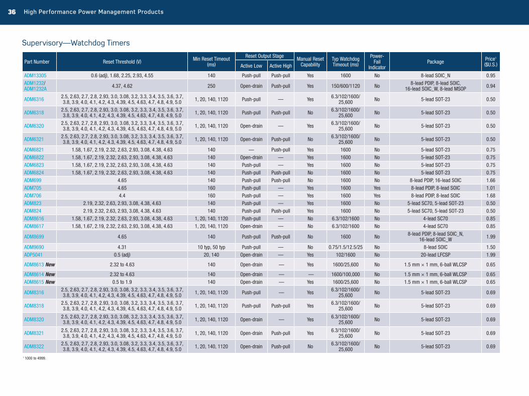
36 High Performance Power Management Products
Supervisory—Watchdog Timers
Part Number Reset Threshold (V) Min Reset Timeout (ms)
Reset Output Stage Manual Reset Capability
Typ Watchdog Timeout (ms)
Power-Fail
IndicatorPackage Price1
($U.S.)Active Low Active High
ADM13305 0.6 (adj), 1.68, 2.25, 2.93, 4.55 140 Push-pull Push-pull Yes 1600 No 8-lead SOIC_N 0.95
ADM1232/ADM1232A 4.37, 4.62 250 Open-drain Push-pull Yes 150/600/1120 No 8-lead PDIP, 8-lead SOIC,
16-lead SOIC_W, 8-lead MSOP 0.94
ADM6316 2.5, 2.63, 2.7, 2.8, 2.93, 3.0, 3.08, 3.2, 3.3, 3.4, 3.5, 3.6, 3.7, 3.8, 3.9, 4.0, 4.1, 4.2, 4.3, 4.39, 4.5, 4.63, 4.7, 4.8, 4.9, 5.0 1, 20, 140, 1120 Push-pull — Yes 6.3/102/1600/
25,600 No 5-lead SOT-23 0.50
ADM6318 2.5, 2.63, 2.7, 2.8, 2.93, 3.0, 3.08, 3.2, 3.3, 3.4, 3.5, 3.6, 3.7, 3.8, 3.9, 4.0, 4.1, 4.2, 4.3, 4.39, 4.5, 4.63, 4.7, 4.8, 4.9, 5.0 1, 20, 140, 1120 Push-pull Push-pull No 6.3/102/1600/
25,600 No 5-lead SOT-23 0.50
ADM6320 2.5, 2.63, 2.7, 2.8, 2.93, 3.0, 3.08, 3.2, 3.3, 3.4, 3.5, 3.6, 3.7, 3.8, 3.9, 4.0, 4.1, 4.2, 4.3, 4.39, 4.5, 4.63, 4.7, 4.8, 4.9, 5.0 1, 20, 140, 1120 Open-drain — Yes 6.3/102/1600/
25,600 No 5-lead SOT-23 0.50
ADM6321 2.5, 2.63, 2.7, 2.8, 2.93, 3.0, 3.08, 3.2, 3.3, 3.4, 3.5, 3.6, 3.7, 3.8, 3.9, 4.0, 4.1, 4.2, 4.3, 4.39, 4.5, 4.63, 4.7, 4.8, 4.9, 5.0 1, 20, 140, 1120 Open-drain Push-pull No 6.3/102/1600/
25,600 No 5-lead SOT-23 0.50
ADM6821 1.58, 1.67, 2.19, 2.32, 2.63, 2.93, 3.08, 4.38, 4.63 140 — Push-pull Yes 1600 No 5-lead SOT-23 0.75
ADM6822 1.58, 1.67, 2.19, 2.32, 2.63, 2.93, 3.08, 4.38, 4.63 140 Open-drain — Yes 1600 No 5-lead SOT-23 0.75
ADM6823 1.58, 1.67, 2.19, 2.32, 2.63, 2.93, 3.08, 4.38, 4.63 140 Push-pull — Yes 1600 No 5-lead SOT-23 0.75
ADM6824 1.58, 1.67, 2.19, 2.32, 2.63, 2.93, 3.08, 4.38, 4.63 140 Push-pull Push-pull No 1600 No 5-lead SOT-23 0.75
ADM699 4.65 140 Push-pull Push-pull No 1600 No 8-lead PDIP, 16-lead SOIC 1.66
ADM705 4.65 160 Push-pull — Yes 1600 Yes 8-lead PDIP, 8-lead SOIC 1.01
ADM706 4.4 160 Push-pull — Yes 1600 Yes 8-lead PDIP, 8-lead SOIC 1.68
ADM823 2.19, 2.32, 2.63, 2.93, 3.08, 4.38, 4.63 140 Push-pull — Yes 1600 No 5-lead SC70, 5-lead SOT-23 0.50
ADM824 2.19, 2.32, 2.63, 2.93, 3.08, 4.38, 4.63 140 Push-pull Push-pull Yes 1600 No 5-lead SC70, 5-lead SOT-23 0.50
ADM8616 1.58, 1.67, 2.19, 2.32, 2.63, 2.93, 3.08, 4.38, 4.63 1, 20, 140, 1120 Push-pull — No 6.3/102/1600 No 4-lead SC70 0.85
ADM8617 1.58, 1.67, 2.19, 2.32, 2.63, 2.93, 3.08, 4.38, 4.63 1, 20, 140, 1120 Open-drain — No 6.3/102/1600 No 4-lead SC70 0.85
ADM8699 4.65 140 Push-pull Push-pull No 1600 No 8-lead PDIP, 8-lead SOIC_N, 16-lead SOIC_W 1.99
ADM9690 4.31 10 typ, 50 typ Push-pull — No 0.75/1.5/12.5/25 No 8-lead SOIC 1.50
ADP5041 0.5 (adj) 20, 140 Open-drain — Yes 102/1600 No 20-lead LFCSP 1.99
ADM8613 New 2.32 to 4.63 140 Open-drain — Yes 1600/25,600 No 1.5 mm × 1 mm, 6-ball WLCSP 0.65
ADM8614 New 2.32 to 4.63 140 Open-drain — — 1600/100,000 No 1.5 mm × 1 mm, 6-ball WLCSP 0.65
ADM8615 New 0.5 to 1.9 140 Open-drain — Yes 1600/25,600 No 1.5 mm × 1 mm, 6-ball WLCSP 0.65
ADM8316 2.5, 2.63, 2.7, 2.8, 2.93, 3.0, 3.08, 3.2, 3.3, 3.4, 3.5, 3.6, 3.7, 3.8, 3.9, 4.0, 4.1, 4.2, 4.3, 4.39, 4.5, 4.63, 4.7, 4.8, 4.9, 5.0 1, 20, 140, 1120 Push-pull — Yes 6.3/102/1600/
25,600 No 5-lead SOT-23 0.69
ADM8318 2.5, 2.63, 2.7, 2.8, 2.93, 3.0, 3.08, 3.2, 3.3, 3.4, 3.5, 3.6, 3.7, 3.8, 3.9, 4.0, 4.1, 4.2, 4.3, 4.39, 4.5, 4.63, 4.7, 4.8, 4.9, 5.0 1, 20, 140, 1120 Push-pull Push-pull Yes 6.3/102/1600/
25,600 No 5-lead SOT-23 0.69
ADM8320 2.5, 2.63, 2.7, 2.8, 2.93, 3.0, 3.08, 3.2, 3.3, 3.4, 3.5, 3.6, 3.7, 3.8, 3.9, 4.0, 4.1, 4.2, 4.3, 4.39, 4.5, 4.63, 4.7, 4.8, 4.9, 5.0 1, 20, 140, 1120 Open-drain — Yes 6.3/102/1600/
25,600 No 5-lead SOT-23 0.69
ADM8321 2.5, 2.63, 2.7, 2.8, 2.93, 3.0, 3.08, 3.2, 3.3, 3.4, 3.5, 3.6, 3.7, 3.8, 3.9, 4.0, 4.1, 4.2, 4.3, 4.39, 4.5, 4.63, 4.7, 4.8, 4.9, 5.0 1, 20, 140, 1120 Open-drain Push-pull Yes 6.3/102/1600/
25,600 No 5-lead SOT-23 0.69
ADM8322 2.5, 2.63, 2.7, 2.8, 2.93, 3.0, 3.08, 3.2, 3.3, 3.4, 3.5, 3.6, 3.7, 3.8, 3.9, 4.0, 4.1, 4.2, 4.3, 4.39, 4.5, 4.63, 4.7, 4.8, 4.9, 5.0 1, 20, 140, 1120 Open-drain Push-pull No 6.3/102/1600/
25,600 No 5-lead SOT-23 0.69
1 1000 to 4999.

36 High Performance Power Management Products Visit analog.com/power 37
Multivoltage Supervisors
Part Number
Number of Monitored Voltages Reset Threshold (V) Min Reset
Timeout (ms)Reset Output Stage Manual Reset
CapabilityTyp Watchdog Timeout (ms) Package Price1
($U.S.)Active Low Active High
ADM13305 2 0.6 (adj), 1.68, 2.25, 2.93, 4.55 140 Push-pull Push-pull Yes 1600 8-lead SOIC_N 0.95
ADM6305 2 0.4 (adj), 1.23 (adj) 1, 20, 140, 1120 Open-drain — — — 5-lead SOT-23 1.15
ADM6306 2 0.4 (adj), 1.23 (adj), 22.5 to 5 (26 options)
1, 20, 140, 1120 Open-drain — — Yes 5-lead SOT-23 1.15
ADM13307 3 0.6 (adj), 1.25 (adj), 1.68, 2.25, 2.93, 4.55 140 Push-pull Push-pull Yes — 8-lead SOIC_N 0.98
ADM6710 3 or 4 0.62 (adj), 1.58, 1.67, 2.19, 2.32, 2.63, 2.78, 2.93, 3.08, 4.38, 4.63 140 Open-drain — No — 6-lead SOT-23 1.60
ADM1184 4 0.6 (adj) 100 Open-drain — No — 10-lead MSOP 1.79
ADM6339 4−0.50 (adj), +0.62 (adj), +1.23 (adj), −4.38, −4.63, +1.58, 2.19, +2.63, +2.78, +2.93,
+3.08, +4.38, +4.63140 Open-drain — No — 6-lead SOT-23 1.79
ADM2914 4 0.5 (adj) Adj Open-drain — — — 16-lead QSOP 2.49
ADM12914 4 0.62 (adj) Adj Open-drain — — — 16-lead QSOP 2.79
ADM8710 4 0.62 (adj), 1.73, 3.07 Adj Open-drain — No — 6-lead SOT-23 1.79 11000 to 4999.
Quad voltage microprocessor supervisory circuit.
IN1
IN2
IN3
IN4
+5.0 V
+3.3 V
+1.8 V
–5.0 V
Reset
GND
ADM6339
Micro-Processor

38 High Performance Power Management Products
Supervisory—Battery Backup
Part Number Reset Threshold (V) Min Reset
Timeout (ms)Reset Output Stage Backup Battery
SwitchChip Enable
GatingTyp Watchdog Timeout (ms) Package Price1
($U.S.)Active Low Active High
ADM690 4.65 35 Push-pull — Yes No 100, 1600 8-lead PDIP 2.39
ADM690A 4.65 140 Push-pull — Yes No 1600 8-lead PDIP, 8-lead SOIC, 8-lead MSOP 1.50
ADM691 4.65 35 adj Push-pull Push-pull Yes Yes 100, 1600, adj 16-lead PDIP, 16-lead SOIC 2.70
ADM691A 4.65 140 adj Push-pull Open-drain Yes Yes 100, 1600, adj 16-lead PDIP, 16-lead SOIC_N, 16-lead SOIC_W, 16-lead TSSOP 1.66
ADM692 4.4 35 Push-pull — Yes No 100, 1600, adj 8-lead PDIP 2.39
ADM692A 4.4 140 Push-pull — Yes No 1600 8-lead PDIP, 8-lead SOIC 1.66
ADM693 4.4 35 adj Push-pull Push-pull Yes Yes 100, 1600, adj 16-lead PDIP, 16-lead SOIC 2.70
ADM693A 4.4 140 adj Push-pull Open-drain Yes Yes 100, 1600, adj 16-lead PDIP, 16-lead SOIC_N, 16-lead SOIC_W 1.83
ADM694 4.65 140 Push-pull — Yes No 100, 1600, adj 8-lead PDIP 2.50
ADM695 4.65 140 adj Push-pull Push-pull Yes Yes 100, 1600, adj 16-lead PDIP, 16-lead SOIC 2.70
ADM696 1.3 adj 35 Push-pull Open-drain Yes No 100, 1600, adj 16-lead PDIP, 16-lead SOIC_W 2.60
ADM697 1.3 adj 35 Push-pull Push-pull No Yes 100, 1600, adj 16-lead PDIP, 16-lead SOIC_W 2.60
ADM800 4.3, 4.55 140 adj Push-pull Open-drain Yes Yes 100, 1600, adj 16-lead PDIP, 16-lead SOIC_N, 16-lead SOIC_W 2.30
ADM802 4.4, 4.65 140 Push-pull — Yes No 1600 8-lead PDIP, 8-lead SOIC 2.20
ADM805 4.4, 4.65 140 — Push-pull Yes No 1600 8-lead PDIP, 8-lead SOIC 2.20
ADM8690 4.65 35 Push-pull — Yes No 1600 8-lead PDIP, 8-lead SOIC 2.49
ADM8691 4.65 35 adj Push-pull Push-pull Yes Yes 100, 1600, adj 16-lead PDIP, 16-lead SOIC_N, 16-lead SOIC_W, 16-lead TSSOP 2.98
ADM8694 4.65 140 Push-pull — Yes No 100, 1600 8-lead PDIP, 8-lead SOIC 2.69
ADM8695 4.65 140 adj Push-pull Push-pull Yes Yes 100, 1600, adj 16-lead SOIC_W 2.16
ADM8696 1.3 adj 35 adj Push-pull Push-pull Yes No 100, 1600, adj 16-lead PDIP, 16-lead SOIC_W, 16-lead TSSOP 2.69
ADM8697 1.3 adj 35 adj Push-pull Push-pull No Yes 100, 1600, adj 16-lead PDIP, 16-lead SOIC_W, 16-lead TSSOP 2.6911000 to 4999.

38 High Performance Power Management Products Visit analog.com/power 39
Low Power Comparators
Part Number Number Per Package
Internal Reference
Reference Accuracy (±%)
Supply Voltage (V)
Supply Current Typ (μA)
Input Range (V)
Propagation Delay Typ (μs) Hysteresis Logic I/O Package Price1
($U.S.)
ADCMP341 2 Yes 0.275 1.7 to 5.5 6.5 0 to VCC 10.0 Adj Open-drain 8-lead SOT-23 0.90
ADCMP343 2 Yes 0.275 1.7 to 5.5 6.5 0 to VCC 10.0 Adj Open-drain 8-lead SOT-23 0.90
ADCMP350 1 Yes 3.5 2.25 to 5.5 10.0 0 to 22 5.0 Internal Open-drain/active low 4-lead SC70 0.31
ADCMP354 1 Yes 3.5 2.25 to 5.5 10.0 0 to 22 5.0 Internal Open-drain/active high 4-lead SC70 0.31
ADCMP356 1 Yes 3.5 2.25 to 5.5 10.0 0 to 22 5.0 Internal Push-pull/active high 4-lead SC70 0.31
ADCMP361 1 Yes 0.275 1.7 to 5.5 6.5 0 to VCC 10.0 Internal Open-drain 5-lead SOT-23 0.60
ADCMP370 1 No — 2.25 to 5.5 4.0 0 to 22 5.0 Internal Open-drain 5-lead SC70 0.28
ADCMP371 1 No — 2.25 to 5.5 4.0 0 to 22 5.0 Internal Push-pull 5-lead SC70 0.28
ADCMP670 2 Yes 1.50 1.7 to 5.5 5.7 0 to VCC 10.0 Internal Open-drain 6-lead TSOT 1.40
ADCMP671 2 Yes 1.50 1.7 to 5.5 5.7 0 to VCC 10.0 Internal Open-drain: PG/OV 6-lead TSOT 1.49
CMP04 4 No — 5 800.0 0 to VCC − 1.5 1.3 — Open-collector 14-lead SOIC 4.75
ADM1184 4 Yes 0.8 2.7 to 5.5 80 0 to VCC 30.0 Fixed Open-drain 10-lead MSOP 1.79
ADM2914 8 Yes 1.5 2.3 to shunt 62 0 to VCC 125 Internal Open-drain 16-lead QSOP 2.49
ADM12914 8 Yes 0.8 2.3 to shunt 62 0 to VCC 125 Internal Open-drain 16-lead QSOP 2.79
ADCMP391 New 1 No — 2.3 to 5.5 18.5 –0.2 to VCC
+ 0.2 5 Internal Open-drain 8-lead SOIC-N 0.25
ADCMP392 New 2 No — 2.3 to 5.5 20.7 –0.2 to VCC
+ 0.2 5 Internal Open-drain 8-lead SOIC-N 0.34
ADCMP393 New 4 Yes — 2.3 to 5.5 26.6 –0.2 to VCC
+ 0.2 5 Internal Open-drain 14-lead SOIC 0.49
ADCMP394 New 1 Yes 0.8 2.3 to 5.5 35 –0.2 to VCC
+ 0.2 5 Internal Open-drain 8-lead SOIC-N 0.37
ADCMP395 New 2 Yes 0.8 2.3 to 5.5 38 –0.2 to VCC + 0.2 5 Internal Open-drain 10-lead MSOP 0.64
ADCMP396 New 4 Yes 0.8 2.3 to 5.5 41.32 –0.2 to VCC + 0.2 5 Internal Open-drain 16-lead SOIC 0.98
ADCMP380 New 1 Yes 1.6 2 to 5.5 0.092 0 to 5.5 23 Internal Open-drain 1.46 mm × 0.96 mm 0.45
1 1000 to 4999.

40 High Performance Power Management Products Visit analog.com/power 41
Li-Ion Battery Monitoring Window Comparator
Quad UV/OV Positive/Negative Monitor
Charging
DischargingVBATT
VOUT
2.280 V
2.271 V
OUT
ADCMP361
INOUT+
400 mV
VDD
3 VLi-IonCell
INH
UV
OVINL
VDD
GND
12 V
RX
RY
RZ
400 mV
ADCMP671 PWRGD
OV
Microprocessor
VH1
VH2
VL2
VH4
5 V3.3 V2.5 V1.8 V
PSU
VL1
VH3
VL3
VL4
SEL
Timer
OV
UV
Latch/DIS
REFGND
VCC
ADM12914System

40 High Performance Power Management Products Visit analog.com/power 41
Isolated PowerIntegrating power supply isolation with data signal isolation has, until recently, been a challenge because of the difficulty of transmitting power from the nonisolated system side to the isolated field side. In the past, transferring power across an isolation barrier required a lot of area, with an expensive module or a complex discrete solution.
Analog Devices has addressed this issue by introducing isoPower®—an extension of the award winning iCoupler® technology. isoPower is a complete and fully integrated isolation solution for power transfer across an isolation barrier using microtransformers. The iCoupler technology enables both signal and power to be integrated into a single, tiny surface-mount package with isolation up to 5 kV.
Isolated switching regulators—another extension of iCoupler technology—provide higher efficiency, power, and board savings over discrete solutions through integration. Features include: secondary side sensing, integrated and isolated feedback, isolated dc-to-dc conversion with up to 80% efficiency, and regulated output voltages between 3.3 V to 30 V.
Digital Isolators with isoPower Integrated, Isolated Power
Part Number
Number of Data Channels
Max Data Rate (Mbps) Max Output Power (mW) Max Temperature (°C) PackageTotal
Reverse Direction Options
0 1 2 3 4
2.5 kV rms IsolationADuM5000* 0 500 @ 5 V 105 16-lead SOIC_W
ADuM5010 0 150 @ 5 V 105 20-lead SSOP
ADuM520x 2 • • • 1, 25 500 @ 5 V 105 16-lead SOIC_W
ADuM521x 2 • • • 1, 25, 100 150 @ 5 V 105 20-lead SSOP
ADuM524x 2 • • • 1 50 @ 5 V 105 8-lead SOIC_N
ADuM540x* 4 • • • • • 1, 25 500 @ 5 V 105 16-lead SOIC_W
3.75 kV rms IsolationADuM6010 0 150 @ 5 V 105 20-lead SSOP
ADuM621x 2 • • • 1, 25, 100 150 @ 5 V 105 20-lead SSOP
5 kV rms IsolationADuM6000 0 400 @ 5 V 105 16-lead SOIC_W/16-lead SOIC_IC
ADuM620x 2 • • • 1, 25 400 @ 5 V 105 16-lead SOIC_W/16-lead SOIC_IC
ADuM640x 4 • • • • • 1, 25 400 @ 5 V 105 16-lead SOIC_W/16-lead SOIC_IC
*Automotive qualified models available. Please visit product pages for more information.
Isolated Switching Regulators
Part Number
Number of Data Channels
Max Data Rate (Mbps)Max Output Power (mW)
Max Temperature (°C) PackageTotal
Reverse Direction OptionsCurrent (mA) Range (V)0 1 2 3 4
2.5 kV rms IsolationADuM3070 0 500 3.3 to 24 105 16-lead QSOP
ADuM347x* 4 • • • • • 1, 25 400 3.3 to 24 105 20-lead SSOP
5 kV rms IsolationADuM4070 0 500 3.3 to 24 105 16-lead SOIC_IC
ADuM447x 4 • • • • • 1, 25 500 3.3 to 24 105 20-lead SOIC_IC
*Automotive qualified models available. Please visit product pages for more information.

42 High Performance Power Management Products Visit analog.com/power 43
Display/Illumination Lighting
High Performance LED Driver SolutionsADI’s wide portfolio of high efficiency and flexible driver ICs targets general illumination and backlighting applications. The portfolio is comprised of buck, boost, charge pump, and sink type LED driver solutions to meet the requirements of almost any input power source. The drivers include special features to ensure a robust and safe design and also have dimming and other control features that maximize the performance of the end application.
Step-Up (Boost) LED Drivers
Part Number VIN (V) VOUT Max (V) Number of Strings Max LEDs Per String
Max Current Per String (mA) Boost Type Switching
Frequency (MHz) I2C Support Package Price @ 1k ($U.S.)
ADP5501 2.7 to 5.5 24 1 6 30 Inductive Variable Yes 24-lead LFCSP 1.20
ADP5520 2.7 to 5.5 24 1 6 30 Inductive Variable Yes 24-lead LFCSP 1.66
ADD5201 6 to 21 45 8 12 30 (240 total) Inductive 1 Yes 28-lead LFCSP 1.40
ADD5203 6 to 21 45 8 12 30 (240 total) Inductive 1 Yes 28-lead LFCSP 1.40
ADD5205 2.8 to 18 28 4 6 25 (100 total) Inductive 1 No 12-lead LFCSP 1.15
ADD5207 6 to 21 36 4 10 25 (100 total) Inductive 1 No 14-lead LFCSP 1.32
ADD5211 3.5 to 40 80 4 22 200 (800 total) Inductive 0.2 to 1.2 No 24-lead LFCSP 1.40
Step-Down (Buck) LED DriversPart Number VIN (V) Number of Strings Max LEDs Per String Max Current Per String (mA) Switching Frequency (MHz) Package Price @ 1k ($U.S.)
ADP2384 4.5 to 20 1 5 4000 0.2 to 1.4 24-lead LFCSP 1.74
ADP2386 4.5 to 20 1 5 6000 0.2 to 1.4 24-lead LFCSP 2.04
ADP2441 4.5 to 36 1 10 1000 0.2 to 1 12-lead LFCSP 1.78
Current Sink LED DriversPart Number VIN (V) Number of Strings Max LEDs Per String Max Current Per String Package Price @ 1k ($U.S.)
ADP8140 Up to 100 4 28 500 mA (2 A total) 16-lead LFCSP 1.50
Inductorless (Charge Pump) LED DriversPart Number VIN (V) VOUT Max (V) Number of Strings LEDs Per String Max Current Per String (mA) Boost Type I2C Support Package Price @ 1k ($U.S.)
ADP8860 2.5 to 5.5 5.5 7 1 30 Charge pump Yes 20-ball WLCSP, 20-lead LFCSP 1.36
ADP8861 2.5 to 5.5 5.5 7 1 30 Charge pump Yes 20-ball WLCSP, 20-lead LFCSP 1.22
ADP8863 2.5 to 5.5 5.5 7 1 30 Charge pump Yes 20-ball WLCSP, 20-lead LFCSP 1.22
ADP8866 2.5 to 5.5 5.5 9 1 25 Charge pump Yes 20-lead LFCSP 1.48
ADP8870 2.5 to 5.5 5.5 7 1 30 Charge pump Yes 20-ball WLCSP, 20-lead LFCSP 1.48
ADM8843 2.6 to 5.5 5.5 4 1 20 Charge pump No 16-lead LFCSP 0.50
ADM8845 2.6 to 5.5 5.5 6 1 30 Charge pump No 16-lead LFCSP 0.71
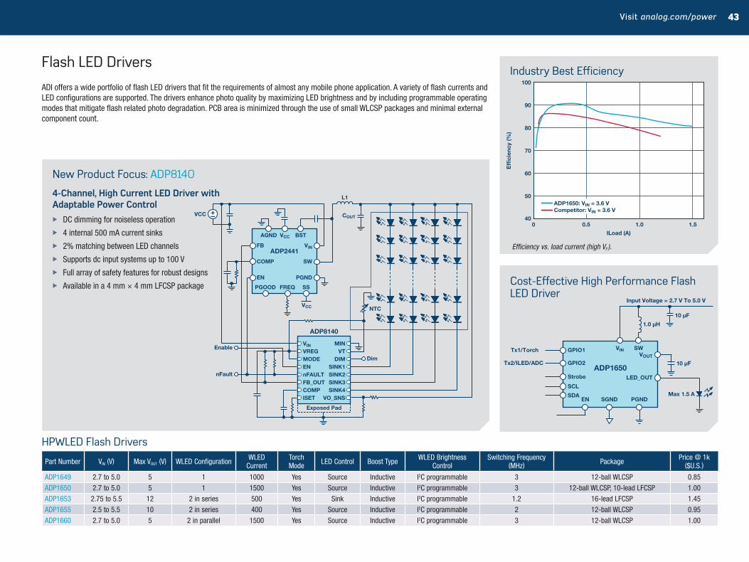
42 High Performance Power Management Products Visit analog.com/power 43
Cost-Effective High Performance Flash LED Driver
New Product Focus: ADP8140
4-Channel, High Current LED Driver with Adaptable Power Control
X DC dimming for noiseless operation
X 4 internal 500 mA current sinks
X 2% matching between LED channels
X Supports dc input systems up to 100 V
X Full array of safety features for robust designs
X Available in a 4 mm × 4 mm LFCSP package
NTC
ADP8140
nFault
Enable
COUT
L1
VCC
ADP2441VIN
SS
EN PGND
SW
FREQPGOOD
FB
COMP
AGND VCC
VCC
BST
VIN
COMP
VREGMODEENnFAULTFB_OUT
MINVT
DIMSINK1SINK2SINK3SINK4
ISET VO_SNS
Dim
Exposed Pad
Flash LED Drivers
ADI offers a wide portfolio of flash LED drivers that fit the requirements of almost any mobile phone application. A variety of flash currents and LED configurations are supported. The drivers enhance photo quality by maximizing LED brightness and by including programmable operating modes that mitigate flash related photo degradation. PCB area is minimized through the use of small WLCSP packages and minimal external component count.
HPWLED Flash Drivers
Part Number VIN (V) Max VOUT (V) WLED Configuration WLED Current
Torch Mode LED Control Boost Type WLED Brightness
ControlSwitching Frequency
(MHz) Package Price @ 1k ($U.S.)
ADP1649 2.7 to 5.0 5 1 1000 Yes Source Inductive I2C programmable 3 12-ball WLCSP 0.85
ADP1650 2.7 to 5.0 5 1 1500 Yes Source Inductive I2C programmable 3 12-ball WLCSP, 10-lead LFCSP 1.00
ADP1653 2.75 to 5.5 12 2 in series 500 Yes Sink Inductive I2C programmable 1.2 16-lead LFCSP 1.45
ADP1655 2.5 to 5.5 10 2 in series 400 Yes Source Inductive I2C programmable 2 12-ball WLCSP 0.95
ADP1660 2.7 to 5.0 5 2 in parallel 1500 Yes Source Inductive I2C programmable 3 12-ball WLCSP 1.00
Industry Best Efficiency
ADP165010 µF
1.0 µH
Input Voltage = 2.7 V To 5.0 V
VOUT
PGND
SW
10 µF
LED_OUT
EN SGND
SCL
SDA
Tx1/Torch
Tx2/ILED/ADC
GPIO1
Strobe
GPIO2
Max 1.5 A
VIN
100
400
Effi
cien
cy (%
)
ILoad (A)
90
80
70
60
50
0.5 1.0 1.5
ADP1650: VIN = 3.6 VCompetitor: VIN = 3.6 V
Efficiency vs. load current (high VF ).
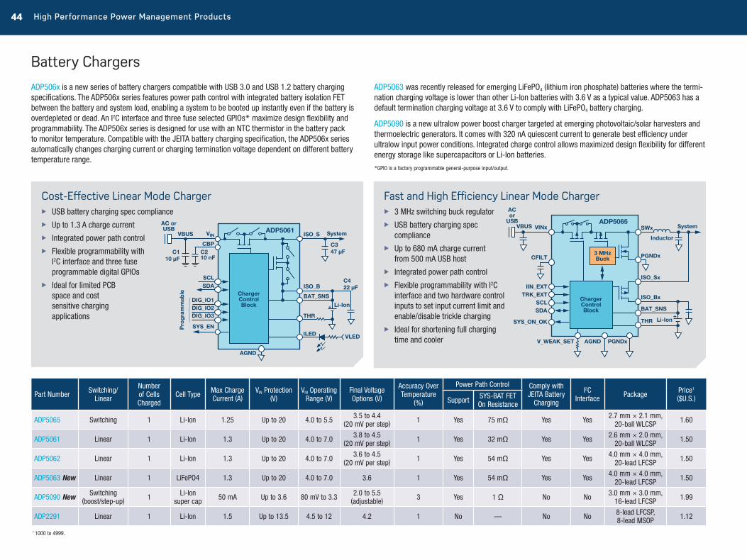
44 High Performance Power Management Products Visit analog.com/power 45
Cost-Effective Linear Mode Charger X USB battery charging spec compliance
X Up to 1.3 A charge current
X Integrated power path control
X Flexible programmability with I2C interface and three fuse programmable digital GPIOs
X Ideal for limited PCB space and cost sensitive charging applications
Fast and High Efficiency Linear Mode Charger X 3 MHz switching buck regulator
X USB battery charging spec compliance
X Up to 680 mA charge current from 500 mA USB host
X Integrated power path control
X Flexible programmability with I2C interface and two hardware control inputs to set input current limit and enable/disable trickle charging
X Ideal for shortening full charging time and cooler
VINVBUS
AC orUSB
SCLSDA
DIG_IO1DIG_IO2DIG_IO3
AGND
+ Li-Ion
THR
C347 µFC2
10 nFC1
10 µF
C422 µF
ISO_S
ISO_B
BAT_SNS
ADP5061
SYS_EN
System
Pro
gra
mm
able
ILED VLED
CBP
ChargerControlBlock
V_WEAK_SET AGND PGNDx
IIN_EXTTRK_EXT
SCLSDA
SYS_ON_OK
ChargerControlBlock
3 MHzBuckCFILT
VINx
PGNDx
ISO_Sx
ISO_Bx
BAT_SNS
THR
SWx
+Li-Ion
VBUS
ACor
USB
Inductor
SystemADP5065
Part Number Switching/Linear
Number of Cells Charged
Cell Type Max Charge Current (A)
VIN Protection (V)
VIN Operating Range (V)
Final Voltage Options (V)
Accuracy Over Temperature
(%)
Power Path Control Comply with JEITA Battery
Charging
I2C Interface Package Price1
($U.S.) Support SYS-BAT FET On Resistance
ADP5065 Switching 1 Li-Ion 1.25 Up to 20 4.0 to 5.5 3.5 to 4.4 (20 mV per step) 1 Yes 75 mΩ Yes Yes 2.7 mm × 2.1 mm,
20-ball WLCSP 1.60
ADP5061 Linear 1 Li-Ion 1.3 Up to 20 4.0 to 7.0 3.8 to 4.5 (20 mV per step) 1 Yes 32 mΩ Yes Yes 2.6 mm × 2.0 mm,
20-ball WLCSP 1.50
ADP5062 Linear 1 Li-Ion 1.3 Up to 20 4.0 to 7.0 3.6 to 4.5 (20 mV per step) 1 Yes 54 mΩ Yes Yes 4.0 mm × 4.0 mm,
20-lead LFCSP 1.50
ADP5063 New Linear 1 LiFePO4 1.3 Up to 20 4.0 to 7.0 3.6 1 Yes 54 mΩ Yes Yes 4.0 mm × 4.0 mm, 20-lead LFCSP 1.50
ADP5090 New Switching (boost/step-up) 1 Li-Ion
super cap 50 mA Up to 3.6 80 mV to 3.3 2.0 to 5.5 (adjustable) 3 Yes 1 Ω No No 3.0 mm × 3.0 mm,
16-lead LFCSP 1.99
ADP2291 Linear 1 Li-Ion 1.5 Up to 13.5 4.5 to 12 4.2 1 No — No No 8-lead LFCSP, 8-lead MSOP 1.12
1 1000 to 4999.
Battery Chargers
ADP506x is a new series of battery chargers compatible with USB 3.0 and USB 1.2 battery charging specifications. The ADP506x series features power path control with integrated battery isolation FET between the battery and system load, enabling a system to be booted up instantly even if the battery is overdepleted or dead. An I2C interface and three fuse selected GPIOs* maximize design flexibility and programmability. The ADP506x series is designed for use with an NTC thermistor in the battery pack to monitor temperature. Compatible with the JEITA battery charging specification, the ADP506x series automatically changes charging current or charging termination voltage dependent on different battery temperature range.
ADP5063 was recently released for emerging LiFePO4 (lithium iron phosphate) batteries where the termi-nation charging voltage is lower than other Li-Ion batteries with 3.6 V as a typical value. ADP5063 has a default termination charging voltage at 3.6 V to comply with LiFePO4 battery charging.
ADP5090 is a new ultralow power boost charger targeted at emerging photovoltaic/solar harvesters and thermoelectric generators. It comes with 320 nA quiescent current to generate best efficiency under ultralow input power conditions. Integrated charge control allows maximized design flexibility for different energy storage like supercapacitors or Li-Ion batteries.
*GPIO is a factory programmable general-purpose input/output.

44 High Performance Power Management Products Visit analog.com/power 45
ALS CMPInputs
Processor
GPIOControl
RegisterInterface
Keypad Controller
Portable ECG
ControlInterface
KeyboardControl
ResetControl
InterruptController
I2CSlave
ALS
GPI
COL[9:0]
ROW[7:0]
SCL
SDA
nRST
nINT
ADP5588
I2C
ADI Keypad Controllers vs. Processor-Based Keypad Controllers ADI Keypad Controllers Processor-Based Keypad Controllers
Typical polling current—55 μA Typical pulling current—60 mA
Only draws current during key press Constant high current drain
Simple board to board interface Complex board to board interface
19
21
23
22
18
1720
24
1 2 3 4 5 6 7 8 9 10 11 12 13 14 15 16
ControlRegisters
ControlInterface
R7
R6
R5
R4
R3
R2
R1
R0
C0
C1
C2
C3
C4
C5
C6
C7
C9
C8
A0A1A2A3A4A5A6A7
B0B1B2B3B4B5B6B7
C0C1C2C3C4C5C6C7
D0D1D2D3D4D5D6D7
E0E1E2E3E4E5E6E7
F0F1F2F3F4F5F6F7
G0G1G2G3G4G5G6G7
H0H1H2H3H4H5H6H7
I0I1I2I3I4I5I6I7
J0J1J2J3J4J5J6J7
SCL
SDA
RST
INT
VCC
GND
VCC
SCL
SDA
ADP5587
RST
INT
Keypad I/O Expanders
ADI’s family of keypad controllers reduces the power consumption in devices while simplifying the design and PCB routing of keypad systems.
Benefits
I/O Expanders and QWERTY Keypad Controllers Part Number VIN (V) Number
of I/OsNumber of Keys
Support for QWERTY Other Functions Package Price @ 1k
($U.S.)
ADP5585 1.8 to 3 16 30 No 10 mA sinks, PWM
generator, logic functions16-ball WLCSP 0.75
ADP5586 1.8 to 3 16 30 No 10 mA sinks, 2 PWM
generators, logic functions16-ball WLCSP 0.75
ADP5587 1.8 to 3 18 80 Yes
I2C interface and register programmable GPIOs,
keypad lock, reset, interrupt
24-lead LFCSP, 25-ball WLCSP
1.15
ADP5588 1.8 to 3 16 80 Yes
I2C interface and register programmable GPIOs, ALS,
reset, interrupt
24-lead LFCSP 1.20
ADP5589 2.5 to 5.5 19 96 Yes
I2C interface and register programmable GPIOs, ALS,
reset, interrupt
24-lead LFCSP, 25-ball WLCSP
1.20
X Reduced power consumption during idle state
X Simplified PCB layout
X Reduced EMI in system
X Decreased GPIO requirements in main PCB
X LFCSP packages for flex PCB mounting

46 High Performance Power Management Products Visit analog.com/power 47
Linear Regulators Switching Regulators Micro-PMUs SC
V IN ( V
)2
2.5
to 5
.5
2.3
to 5
.5
2.3
to 5
.5
2.2
to 5
.5
2.2
to 5
.5
1.6
to 3
.6
2.5
to 5
.5
2.5
to 5
.5
2.5
to 5
.5
2.5
to 5
.5
4.0
to 2
8
1.6
to 3
.6
1.6
to 3
.6
1.6
to 3
.6
2.7
to 5
.5
2.7
to 5
.5
2.7
to 5
.5
2.3
to 5
.5
2.7
to 5
.5
2.7
to 5
.5
2.3
to 5
.5
2.3
to 5
.5
2.3
to 5
.5
3.2
to 1
5
Buck
: 2.3
to 5
.5;
LDO:
1.7
to 5
.5
Buck
: 2.3
to 5
.5;
LDO:
1.7
to 5
.5
Buck
: 2.3
to 5
.5;
LDO:
1.7
to 5
.5
Buck
: 2.3
to 5
.5;
LDO:
1.7
to 5
.5
Buck
: 2.3
to 5
.5;
LDO:
1.7
to 5
.5
Buck
: 3.0
to 5
.5
Buck
: 2.3
to 5
.5;
LDO:
1.7
to 5
.5
3.0
to 1
8
3.15
to 1
4
V OUT
( V)
1.2
to 3
.3
0.8
to 5
.0
0.8
to 5
.0
1.2
to 3
.3
1.2
to 4
.2
0.8
to 3
.0
0.8
to 2
.8
0.75
to 3
.3,
soft
star
t
0.75
to 3
.3,
with
trac
king
0.8
to 5
.0
1.22
5 to
5.0
0.75
to 3
.0
0.75
to 2
.5
0.75
to 2
.5
0.8
to 1
.785
1.2
to 3
.3
1.2
to 3
.3
1.0
to 3
.3
0.8
to 3
.3
0.8
to 3
.3
1.0
to 3
.3
1.0
to 3
.3
2.8
to 5
.0
0.8
to 5
.0
0.8
to 3
.8
0.8
to 3
.8
0.8
to 3
.8
0.8
to 3
.8
0.8
to 3
.8
0.8
to 3
.8
0.8
to 3
.8
0.6
to 1
5.3
0.8
to 1
4
I OUT M
ax ( m
A)1
150
300
500
200
150
300
2 ou
tput
s: 2
00, 2
00
1000
1000
500
50 2000
800
1200
600
1500
2000
600
4000
3000
800
2 ou
tput
s: 6
00, 3
00
1000
800
SW: 8
00, 8
00;
LDO:
300
SW: 1
.2 A
, 1.2
A;
LDO:
300
SW: 1
.2 A
, 1.2
A;
LDO:
300
, 300
SW: 8
00, 8
00;
LDO:
300
, 300
SW: 1
.2 A
; LD
O: 3
00, 3
00
SW: 1
.8 A
SW: 1
.2 A
; LD
O: 3
00, 3
00
30 A
8 A
Part
Num
ber
ADP1
21
ADP1
23
ADP1
25
ADP1
51
ADP1
60
ADP1
70
ADP2
20, 2
LDO
s
ADP1
706
ADP1
707
ADP1
715
ADP1
720
ADP1
740,
ADP
1741
ADP1
752,
ADP
1753
ADP1
754,
ADP
1755
ADP2
102
ADP2
106
ADP2
107
ADP2
108
ADP2
114
ADP2
118
ADP2
138
ADP2
140,
1 b
uck,
1
LDO
ADP2
504
ADP2
370
ADP5
023,
2 b
ucks
, 1
LDO
ADP5
024,
2 b
ucks
, 1
LDO
ADP5
134,
2 b
ucks
, 2
LDOs
ADP5
037,
2 b
ucks
, 2
LDOs
ADP5
040,
1 b
uck,
2
LDOs
ADP5
135,
3 b
ucks
ADP5
041,
1 b
uck,
2
LDOs
ADP1
829
ADP1
864
VDD I
NT D
omai
n
Blackfin Processors
Speed (MHz)
Min Voltage
(V)
Max Voltage
(V)Max IDDINT (mA)
ADSP-BF50x All 1.1 1.47 175 • • • • • • • • • • • • • • • •
ADSP-BF51x All 1.1 1.47 225 • • • • • • • • • • • • • • • •
ADSP-BF522/ADSP-BF524/ADSP-BF526 All 1.235 1.47 250 • • • • • • • • • • • • • • • •
ADSP-BF523/ADSP-BF525/ADSP-BF527 All 0.95 1.26 500 • • • • • • • • • • • • • • • • • •
ADSP-BF531/ADSP-BF532/ADSP-BF533 400 0.8 1.32 350 • • • • • • • • • • • • • • •
ADSP-BF533 500, 533, 600 0.8 1.45 900 • • • •3 • • •3 • • •
ADSP-BF534/ADSP-BF536 300, 400 0.8 1.32 400 • • • • • • • • • • • • • • •
ADSP-BF534/ADSP-BF536/ADSP-BF537 500, 533, 600 0.8 1.43 900 • • • • • •3 • • •3 • • •
ADSP-BF538/ADSP-BF539 400, 533 0.8 1.375 850 • • • • • •3 • • •3 • • •
ADSP-BF54x 400 0.9 1.43 750 • • • • • • • • • • • • • • •
ADSP-BF54x 533, 600 0.9 1.43 1350 • • • •3 •3 •3 •3 •3
ADSP-BF561 All 0.8 1.42 1600 • • •
ADSP-BF592 All 1.1 1.47 150 • • • • • • • • • • • • • • • •
ADSP-BF60x All 1.1875 1.3125 1000 • • • • • • •3 • • •3 • • •
Othe
r Dom
ains
Min Voltage
(V)
Nom Voltages
(V)
Max Voltage
(V)Max Current (mA)
VDDEXT 1.8, 2.5, 3.3 N/A • • • • • • • • • • • • • • • • • • • • • • •
VDDMEM 1.8, 2.5, 3.3 N/A • • • • • • • • • • • • • • • • • • • • • • • •
VDDDDR 2.6 N/A • • • • • • • • • • • • • • • • • • • • • • • • • • •
VDD_DMC 1.8 N/A •4 •4 • •4 • • • • • •4 •4 •4 •4 •4 •4 •4 •4
VDDUSB 3.3 30 • • • • • • • • • • • • • • • • • • • • • • • •
VDDOTP 2.5 25 • • • • • • • • • • • • • • • • • • • • • • • • • • • • • •
Reset/Watchdog Support •
1 In micro-PMUs the larger current value refers to bucks while the lower number refers to LDOs. 2 In the micro-PMU case the two voltage ranges refer to the bucks and LDOs respectively. 3 Not all the speed versions supported. 4 Assumes low power DDR2 memories.
DSP Companion GuideCompanion Power Selection Guide: Blackfin ProcessorsADI power management products provide optimized power for Blackfin®, SHARC®, and microcontroller products—whether it’s a single processor or multiple processors, in handheld or high power applications, ADI has a solution to meet your needs.
How to Use This GuideDetermine the peak current requirement for each rail of your processor by referring to the relevant data sheets and engineer-to-engineer notes. The ADIsimPower design tool offers a complete set of features to create a complete BOM for all of these solutions. Visit www.analog.com/ADIsimPower.
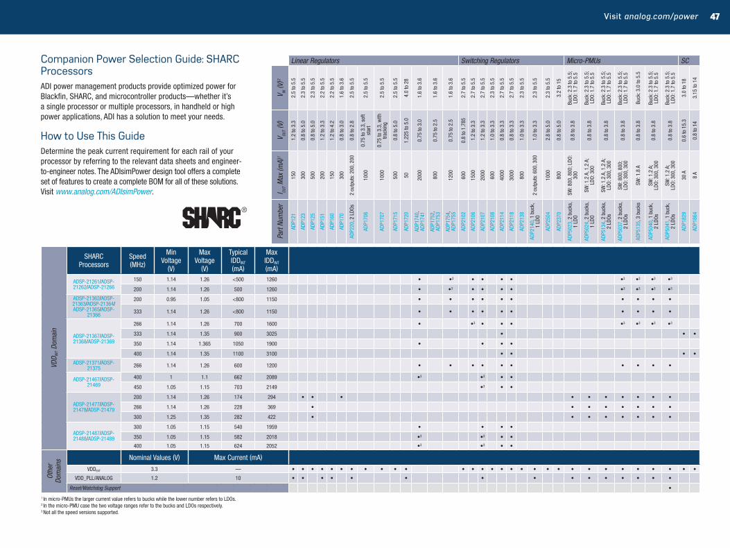
46 High Performance Power Management Products Visit analog.com/power 47
Companion Power Selection Guide: SHARC Processors
Linear Regulators Switching Regulators Micro-PMUs SC
V IN ( V
)2
2.5
to 5
.5
2.3
to 5
.5
2.3
to 5
.5
2.2
to 5
.5
2.2
to 5
.5
1.6
to 3
.6
2.5
to 5
.5
2.5
to 5
.5
2.5
to 5
.5
2.5
to 5
.5
4.0
to 2
8
1.6
to 3
.6
1.6
to 3
.6
1.6
to 3
.6
2.7
to 5
.5
2.7
to 5
.5
2.7
to 5
.5
2.3
to 5
.5
2.7
to 5
.5
2.7
to 5
.5
2.3
to 5
.5
2.3
to 5
.5
2.3
to 5
.5
3.2
to 1
5
Buck
: 2.3
to 5
.5;
LDO:
1.7
to 5
.5
Buck
: 2.3
to 5
.5;
LDO:
1.7
to 5
.5
Buck
: 2.3
to 5
.5;
LDO:
1.7
to 5
.5
Buck
: 2.3
to 5
.5;
LDO:
1.7
to 5
.5
Buck
: 3.0
to 5
.5
Buck
: 2.3
to 5
.5;
LDO:
1.7
to 5
.5
Buck
: 2.3
to 5
.5;
LDO:
1.7
to 5
.5
3.0
to 1
8
3.15
to 1
4
V OUT ( V
)
1.2
to 3
.3
0.8
to 5
.0
0.8
to 5
.0
1.2
to 3
.3
1.2
to 4
.2
0.8
to 3
.0
0.8
to 2
.8
0.75
to 3
.3, s
oft
star
t
0.75
to 3
.3, w
ith
track
ing
0.8
to 5
.0
1.22
5 to
5.0
0.75
to 3
.0
0.75
to 2
.5
0.75
to 2
.5
0.8
to 1
.785
1.2
to 3
.3
1.2
to 3
.3
1.0
to 3
.3
0.8
to 3
.3
0.8
to 3
.3
1.0
to 3
.3
1.0
to 3
.3
2.8
to 5
.0
0.8
to 5
.0
0.8
to 3
.8
0.8
to 3
.8
0.8
to 3
.8
0.8
to 3
.8
0.8
to 3
.8
0.8
to 3
.8
0.8
to 3
.8
0.6
to 1
5.3
0.8
to 1
4
I OUT M
ax ( m
A)1
150
300
500
200
150
300
2 ou
tput
s: 2
00, 2
00
1000
1000
500
50 2000
800
1200
600
1500
2000
600
4000
3000
800
2 ou
tput
s: 6
00, 3
00
1000
800
SW: 8
00, 8
00; L
DO:
300
SW: 1
.2 A
, 1.2
A;
LDO:
300
SW: 1
.2 A
, 1.2
A;
LDO:
300
, 300
SW: 8
00, 8
00;
LDO:
300
, 300
SW: 1
.8 A
SW: 1
.2 A
; LD
O: 3
00, 3
00
SW: 1
.2 A
; LD
O: 3
00, 3
00
30 A
8 A
Part
Num
ber
ADP1
21
ADP1
23
ADP1
25
ADP1
51
ADP1
60
ADP1
70
ADP2
20, 2
LDO
s
ADP1
706
ADP1
707
ADP1
715
ADP1
720
ADP1
740,
AD
P174
1
ADP1
752,
AD
P175
3
ADP1
754,
AD
P175
5
ADP2
102
ADP2
106
ADP2
107
ADP2
108
ADP2
114
ADP2
118
ADP2
138
ADP2
140,
1 b
uck,
1
LDO
ADP2
504
ADP2
370
ADP5
023,
2 b
ucks
, 1
LDO
ADP5
024,
2 b
ucks
, 1
LDO
ADP5
134,
2 b
ucks
, 2
LDOs
ADP5
037,
2 b
ucks
, 2
LDOs
ADP5
135,
3 b
ucks
ADP5
040,
1 b
uck,
2
LDOs
ADP5
041,
1 b
uck,
2
LDOs
ADP1
829
ADP1
864
VDD I
NT D
omai
n
SHARC Processors
Speed (MHz)
Min Voltage
(V)
Max Voltage
(V)
Typical IDDINT (mA)
Max IDDINT (mA)
ADSP-21261/ADSP-21262/ADSP-21266
150 1.14 1.26 <500 1260 • •3 • • • • •3 •3 •3 •3
200 1.14 1.26 500 1260 • •3 • • • • •3 •3 •3 •3
ADSP-21362/ADSP-21363/ADSP-21364/ADSP-21365/ADSP-
21366
200 0.95 1.05 <800 1150 • • • • • • • • • •
333 1.14 1.26 <800 1150 • • • • • • • • • •
ADSP-21367/ADSP-21368/ADSP-21369
266 1.14 1.26 700 1600 • •3 • • • •3 •3 •3 •3
333 1.14 1.35 900 3025 • • •
350 1.14 1.365 1050 1900 • • • •
400 1.14 1.35 1100 3100 • • • •
ADSP-21371/ADSP-21375 266 1.14 1.26 600 1200 • • • • • • • • • •
ADSP-21467/ADSP-21469
400 1 1.1 662 2089 •3 •3 • •
450 1.05 1.15 703 2149 •3 • •
ADSP-21477/ADSP-21478/ADSP-21479
200 1.14 1.26 174 294 • • • • • • • • • •
266 1.14 1.26 228 369 • • • • • • • •
300 1.25 1.35 282 422 • • • • • • • •
ADSP-21487/ADSP-21488/ADSP-21489
300 1.05 1.15 540 1959 • • • •
350 1.05 1.15 582 2018 •3 •3 • •
400 1.05 1.15 624 2052 •3 •3 • •
Othe
r Do
mai
ns
Nominal Values (V) Max Current (mA)
VDDEXT 3.3 — • • • • • • • • • • • • • • • • • • • • • • • • • • • • • •
VDD_PLL/ANALOG 1.2 10 • • • • • • • • • • • • • • •
Reset/Watchdog Support •
1 In micro-PMUs the larger current value refers to bucks while the lower number refers to LDOs. 2 In the micro-PMU case the two voltage ranges refer to the bucks and LDOs respectively. 3 Not all the speed versions supported.
Companion Power Selection Guide: SHARC Processors ADI power management products provide optimized power for Blackfin, SHARC, and microcontroller products—whether it’s a single processor or multiple processors, in handheld or high power applications, ADI has a solution to meet your needs.
How to Use This GuideDetermine the peak current requirement for each rail of your processor by referring to the relevant data sheets and engineer-to-engineer notes. The ADIsimPower design tool offers a complete set of features to create a complete BOM for all of these solutions. Visit www.analog.com/ADIsimPower.

Analog Devices, Inc. Worldwide Headquarters
Analog Devices, Inc. One Technology Way P.O. Box 9106 Norwood, MA 02062-9106 U.S.A. Tel: 781.329.4700 (800.262.5643, U.S.A. only) Fax: 781.461.3113
Analog Devices, Inc. Europe Headquarters
Analog Devices, Inc. Wilhelm-Wagenfeld-Str. 6 80807 Munich Germany Tel: 49.89.76903.0 Fax: 49.89.76903.157
Analog Devices, Inc. Japan Headquarters
Analog Devices, KK New Pier Takeshiba South Tower Building 1-16-1 Kaigan, Minato-ku, Tokyo, 105-6891 Japan Tel: 813.5402.8200 Fax: 813.5402.1064
Analog Devices, Inc. Asia Pacific Headquarters
Analog Devices 5F, Sandhill Plaza 2290 Zuchongzhi Road Zhangjiang Hi-Tech Park Pudong New District Shanghai, China 201203 Tel: 86.21.2320.8000 Fax: 86.21.2320.8222
©2016 Analog Devices, Inc. All rights reserved. Trademarks and registered trademarks are the property of their respective owners.Ahead of What’s Possible is a trademark of Analog Devices.Printed in the U.S.A. BR06616-.1-3/16(I)
analog.com/power
Online Tools and Resources
In addition to providing world-class products and technical support, ADI takes great pride in offering design engineers the very best in online design tools. These tools have been specifically designed to provide power designers and nonpower designers alike the tools needed to design, optimize, and implement the very best power circuits available.
Tools like the recently released ADIsimPower tool provide users with an easy four-step process using an intuitive graphical user interface via your Web browser. This particular tool allows the designer to preselect their key goals, whether they be cost, size, or performance, and optimizes the solution to meet those goals. Additional tools are available online (as Excel-based downloadable versions) that make product selection and design a snap. ADI puts the power back in your hands.
Available Online Tools X ADIsimPE: linear and mixed-signal circuit simulator
X ADIsimPower: part selection and design tool
X Parametric search tools for linear regulators, supervisors, and others
X Design and control tools for hot swap, digital power, and sequencers
Other Power Brochures Available: X High Performance LDOs
X Hot Swap and Power Monitoring
X Integrated Power Management Solutions
X Integrated Power Solutions for Xilinx FPGAs
X Integrated Power Solutions for Altera FPGAs
X Voltage Monitoring and Sequencing
X Digital Isolator Product Selection and Resource Guide
EngineerZone Online Support CommunityFind answers to your power management questions. Join our power management community at ez.analog.com.
External Trigger
FMC Connector
ADC Inputs ADC
Inputs
DAC Outputs DAC
Outputs
ADN4661 Buffer
ADP1503 1.2 A LDO
ADP1753 Ultralow Noise 150 MA LDO
ADP2384 4 A Switcher
ADN4661 Buffer
AD7291 8-CH ADC
ADP1740-1.2 2 A LDO
AD9144 DAC 16-Bit
25 GSPS
AD9680 ADC 14-Bit
1 GSPS125 MHz Crystal
AD9523-1 Low Jitter Clock
Generator
ADP7104-3.3 High Accuracy 500 mA LDO
Proven reference design.


