High-performance transimpedance formulation for MESFET- and HBT-based monolithic microwave integrated circuits B. Wilson J.D. Drew Indexing terms: Trunsimpeclance, MESFET, H B T , Microwave integrated circuits Abstract: Analysis of amplifier and feedback combinations leads to the conclusion that the transimpedance configuration offers the opportunity of constant-bandwidth operation. As an example, a transimpedance amplifier based on shunt feedback around a current-gain amplifying element is described, which achieves gain-bandwidth independence at microwave frequencies. Full foundry layout simulation for circuits based on both MESFETs and HBTs indicates that an optical receiver front-end amplifier designed on these principles will exhibit gain-bandwidth independence through the GHz region, with very low sensitivity to photodiode capacitance. 1 introduction Definition of amplifier gain without compromising bandwidth is a highly desirable design aim. Recently, this has been achieved for voltage amplification at lower frequencies through the use of a buffered current amplifier within an overall feedback arrangement, known as ‘current-feedback’ [14]. In this paper we show that the benefit of constant-bandwidth operation can be extended to a much wider range of amplifier configurations. In particular, a transimpedance ampli- fier formulated by applying shunt feedback around a current amplifier is found to display gain-bandwidth independence at frequencies through to the microwave region, where it is directly applicable to monolithic microwave integrated circuits (MMICs). High-speed transimpedance formulations are of par- ticular interest to designers of direct-detection optical systems, since the major constraints on bandwidth and noise usually arise in the immediate post-detector elec- tronic processing stage and its interaction with the pho- todetector [5, 61. Transimpedance amplifiers, rather than high-impedance stages, are preferred in this role 0 IEE, 1998 IEE Proceedings online no. 19982392 Paper first received 19 December 1997 and in revised form 7 July 1998 B. Wilson is with the Department of Electrical Engineering and Electron- ics, University of Manchester Institute of Science & Technology (UMIST), PO Box 88, Manchester M60 lQD, UK J.D. Drew is with Cadence Design Systems, Spectrum Services, North Lake, Bracknell, Berks RG12 7WH, UK because they are intrinsically less sensitive to photodi- ode and parasitic capacitance as a result of their lower input impedance, as well as providing a wider and flat- ter gain profile [6]. To achieve the closest approach to an ideal transimpedance formulation, an amplifier design should already exhibit a low input impedance, even before the application of feedback, suggesting the use of common-base or common-gate input configura- tions [7]. Within this general low-input-impedance framework, a number of closely related transimpedance designs have been reported in recent years, each seek- ing to further optimise internal circuit conditions and configurations for lower noise and bandwidth exten- sion over a range of different semiconductor technolo- gies [7-151. However, none of the previously reported transim- pedance formulations or circuits have exhibited the ability to avoid the restriction of a constant gain-band- width product and define amplifier gain without com- promising bandwidth, as demonstrated by current feedback amplifiers (CFAs) and current conveyor based structures, exploiting a loop gain that is inde- pendent of the required closed-loop gain [14, 161. The approach developed in this paper exploits the fact that constant-bandwidth behaviour is potentially available whenever the overall feedback configuration and amplifying element are of a dissimilar type [17-201, in this case allowing a transimpedance amplifier using shunt feedback around a current amplifier to display constant-bandwidth behaviour into the microwave region. Results are presented from full-layout circuit simulation of two different amplifiers, based on detailed foundry models for MESFET and HBT devices, respectively. 2 Analysis The requirement of a particular stabilised response function for a system configuration determines the type of feedback arrangement, but does not restrict the choice of amplifying element type, which may be inde- pendently chosen. Analysis of the four possible differ- ent feedback arrangements and the four active amplifying element types provides a complete range of gain-defining equations [ 17-20], from which the behav- iour of the loop-gain term can be used to investigate bandwidth behaviour, as in Table 1 [17, 20, 211. Of the 16 combinations, the 4 cases for which the feedback arrangement and the amplifier are of the same type all generate a fixed gain-bandwidth product, since the 429 1EE Proc.-Circuits Devices Syst , Vol. 145, No. 6. December I998
Transcript
High-performance transimpedance formulation for MESFET- and HBT-based monolithic microwave integrated circuits
Abstract: Analysis of amplifier and feedback combinations leads to the conclusion that the transimpedance configuration offers the opportunity of constant-bandwidth operation. As an example, a transimpedance amplifier based on shunt feedback around a current-gain amplifying element is described, which achieves gain-bandwidth independence at microwave frequencies. Full foundry layout simulation for circuits based on both MESFETs and HBTs indicates that an optical receiver front-end amplifier designed on these principles will exhibit gain-bandwidth independence through the GHz region, with very low sensitivity to photodiode capacitance.
1 introduction
Definition of amplifier gain without compromising bandwidth is a highly desirable design aim. Recently, this has been achieved for voltage amplification at lower frequencies through the use of a buffered current amplifier within an overall feedback arrangement, known as ‘current-feedback’ [14]. In this paper we show that the benefit of constant-bandwidth operation can be extended to a much wider range of amplifier configurations. In particular, a transimpedance ampli- fier formulated by applying shunt feedback around a current amplifier is found to display gain-bandwidth independence at frequencies through to the microwave region, where it is directly applicable to monolithic microwave integrated circuits (MMICs).
High-speed transimpedance formulations are of par- ticular interest to designers of direct-detection optical systems, since the major constraints on bandwidth and noise usually arise in the immediate post-detector elec- tronic processing stage and its interaction with the pho- todetector [5 , 61. Transimpedance amplifiers, rather than high-impedance stages, are preferred in this role
0 IEE, 1998 IEE Proceedings online no. 19982392 Paper first received 19 December 1997 and in revised form 7 July 1998 B. Wilson is with the Department of Electrical Engineering and Electron- ics, University of Manchester Institute of Science & Technology (UMIST), PO Box 88, Manchester M60 lQD, UK J.D. Drew is with Cadence Design Systems, Spectrum Services, North Lake, Bracknell, Berks RG12 7WH, UK
because they are intrinsically less sensitive to photodi- ode and parasitic capacitance as a result of their lower input impedance, as well as providing a wider and flat- ter gain profile [6]. To achieve the closest approach to an ideal transimpedance formulation, an amplifier design should already exhibit a low input impedance, even before the application of feedback, suggesting the use of common-base or common-gate input configura- tions [7]. Within this general low-input-impedance framework, a number of closely related transimpedance designs have been reported in recent years, each seek- ing to further optimise internal circuit conditions and configurations for lower noise and bandwidth exten- sion over a range of different semiconductor technolo- gies [7-151.
However, none of the previously reported transim- pedance formulations or circuits have exhibited the ability to avoid the restriction of a constant gain-band- width product and define amplifier gain without com- promising bandwidth, as demonstrated by current feedback amplifiers (CFAs) and current conveyor based structures, exploiting a loop gain that is inde- pendent of the required closed-loop gain [ 1 4 , 161. The approach developed in this paper exploits the fact that constant-bandwidth behaviour is potentially available whenever the overall feedback configuration and amplifying element are of a dissimilar type [17-201, in this case allowing a transimpedance amplifier using shunt feedback around a current amplifier to display constant-bandwidth behaviour into the microwave region. Results are presented from full-layout circuit simulation of two different amplifiers, based on detailed foundry models for MESFET and HBT devices, respectively.
2 Analysis
The requirement of a particular stabilised response function for a system configuration determines the type of feedback arrangement, but does not restrict the choice of amplifying element type, which may be inde- pendently chosen. Analysis of the four possible differ- ent feedback arrangements and the four active amplifying element types provides a complete range of gain-defining equations [ 17-20], from which the behav- iour of the loop-gain term can be used to investigate bandwidth behaviour, as in Table 1 [17, 20, 211. Of the 16 combinations, the 4 cases for which the feedback arrangement and the amplifier are of the same type all generate a fixed gain-bandwidth product, since the
loop gain is inversely dependent on the closed-loop demanded gain, resulting in reduced bandwidth at higher gain. For the other 12 combinations, only those involving VCVS (voltage) and CCCS (current) amplify- ing elements provide true gain-bandwidth independ- ence, whereas the combinations involving CCVS (transimpedance) and VCCS (transconductance) ele- ments will exhibit this feature only under certain condi- tions of gain-defining components [20, 211. In general, source or load buffering will be required to obtain con- stant-bandwidth operation, because of the unusual matching conditions. Of particular interest are the underlined cases, in which the amplifying element itself naturally provides an optimised input parameter for the overall configuration, leaving only the output stage to be buffered, since in this way noise performance degradation is avoided. However, of the 4 combina- tions underlined in Table 1 which display this feature, only the transimpedance and transconductance config- urations (shown both bold and underlined) will exhibit true constant-bandwidth behaviour with no direct dependence on feedback component values, and so provide the widest range of new design opportunities.
The description of constant loop-gain feedback cir- cuits may be applied to this general class of constant- bandwidth circuits to distinguish them from the poten- tially ambiguous category of ‘current-mode’ circuits. The term ‘current-mode’ was originally used to describe circuits that deliberately set out to use current rather than voltage for signal representation, but has been applied rather indiscriminately of late to circuits that perhaps should be more accurately termed ‘mixed- mode’ circuits, in that they rely on both current and voltage signal representation for their operation.
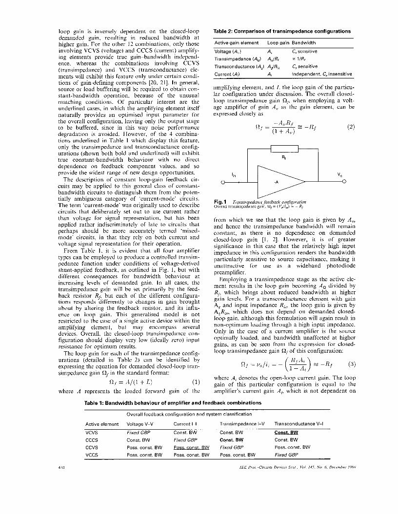
From Table 1, it is evident that all four amplifier types can be employed to produce a controlled transim- pedance function under conditions of voltage-derived shunt-applied feedback, as outlined in Fig. 1, but with different consequences for bandwidth behaviour at increasing levels of demanded gain. In all cases, the transimpedance gain will be set primarily by the feed- back resistor Rf, but each of the different configura- tions responds differently to changes in gain brought about by altering the feedback resistor, and its influ- ence on loop gain. This generalised model is not restricted to the case of a single active device within the amplifying element, but may encompass several devices. Overall, the closed-loop transimpedance con- figuration should display very low (ideally zero) input resistance for optimum results.
The loop gain for each of the transimpedance config- urations (detailed in Table 2) can be identified by expressing the equation for demanded closed-loop tran- simpedance gain Qf in the standard format:
where A represents the loaded forward gain of the Rf = A / ( 1 + L ) (1)
’in
Table 2: Comparison of transimpedance configurations
b
“0
Active gain element Loop gain Bandwidth
Voltage (A,) A” C, sensitive
Transimpedance (A,) A$Rf l/Rf
Transconductance (A,) AJR,, C, sensitive
Current (A,) A, Independent, C, insensitive
amplifying element, and L the loop gain of the particu- lar configuration under discussion. The overall closed- loop transimpedance gain Qzf. when employing a volt- age amplifier of gain A,, as the gain element, can be expressed closely as
from which we see that the loop gain is given by AV, and hence the transimpedance bandwidth will remain constant, as there is no dependence on demanded closed-loop gain [ I , 21. However, it is of greater significance in this case that the relatively high input impedance in this configuration renders the bandwidth particularly sensitive to source capacitance, making it unattractive for use as a wideband photodiode preamplifier.
Employing a transimpedance stage as the active ele- ment results in the loop gain becoming A, divided by RP which brings about reduced bandwidth at higher gain levels. For a transconductance element with gain A, and input impedance Ri,, the loop gain is given by A,R,,, which does not depend on demanded closed- loop gain, although this formulation will again result in non-optimum loading through a high input impedance. Only in the case of a current amplifier is the source optimally loaded, and bandwidth unaffected at higher gains, as can be seen from the expression for closed- loop transimpedance gain Qf of this configuration:
where Ai denotes the open-loop current gain. The loop gain of this particular configuration is equal to the amplifier’s current gain A , which is not dependent on
Table 1: Bandwidth behaviour of amplifier and feedback combinations
Overall feedback configuration and system classification
Active element Voltage V-V Current 1-1 Transimpedance I-V Transconductance V-l
the demanded closed-loop transimpedance gain of the system through Rr; the circuit will therefore exhibit a constant bandwidth irrespective of demanded closed- loop gain. (The forward gain of the configuration, in this case A;Rf, will increase in direct proportion to the demanded closed-loop gain, in contrast to constant- gain-bandwidth configurations, where it would remain constant and be determined only by the amplifying ele- ment itself). In addition, because of the very low input resistance, enhanced through the particular combina- tion of current amplifier and shunt feedback, the band- width will display very low sensitivity to source and parasitic input capacitance.
To achieve gain-bandwidth independence for a tran- simpedance amplifier, it is therefore advisable to for- mulate it from a current gain element, as summarised in Table 2. Taking the amplifier's (low) input resistance RI,, into account results in a reduced loaded forward gain and modifies eqn. 3 to become [22]:
50
c: 45
%! 40 ._ r 35 5 30 2 25-
20- ._ 15- U) 5 10- -
0
M -Rf (4) R f Ai - Ri, ( 1+Ai
Rf = vo/& = - r F$ = 300R
180R lOOR 55R 30*
5- I I
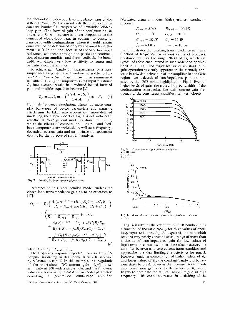
For high-frequency simulation, where the more com- plex behaviour of device parameters and parasitic effects must be taken into account with more detailed modelling, the simple model of Fig. 1 is not sufficiently realistic. A more general model is shown in Fig. 2, where the effects of complex input, output and feed- back components are included, as well as a frequency- dependent current gain and an intrinsic transportation delay z for the purpose of stability analysis.
intrinsic current amplifier Detailed feedback trcmsinipedance nzodel Fig. 2
Reference to this more detailed model enables the closed-loop transimpedance gain Qj to be expressed as [17]:
where CT = Cf f C,orrrl + CO,,. The frequency response expected from an amplifier
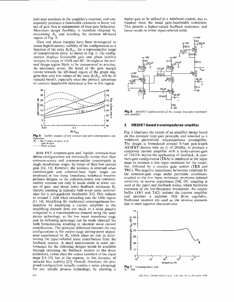
designed according to this approach may be assessed by reference to eqn. 5. In this example, the magnitude of the short-circuit DC current gain IAi(w)l is set arbitrarily at 200 with a single pole, and the following values are taken as representative for model parameters describing a generalised multi-stage amplifier,
IEE Proc.-Circuits Device., Syst., Vol. 145, No. 6, December 1998
35 r
N I U
o s m n m '?
G-
U
U
Fig.4 t = s p s
Fig
l o 5 1 I I
0.01 0.1 1
R,/ R0"t
Bunditidtli as U function of noriria1isedfeedbut.k resistcince
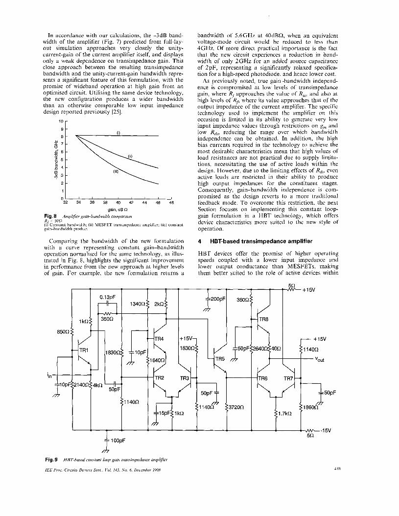
4 illustrates the variation in -3dB bandwidth as a function of the ratio RrlRo,,, for three values of open- loop input resistance R,,,. As expected, the bandwidth remains very nearly constant over a range of more than a decade of transimpedance gain for low values of input resistance, because under these circumstances, the amplifier behaves as a true current-input amplifier and approaches the ideal limiting characteristics for eqn. 3. However, under a combination of higher values of RI,, and lower values of RP the constant-bandwidth behav- iour starts to break down as the increased transimped- ance conversion gain due to the action of R, alone begins to dominate the reduced amplifier gain at high frequency. This condition results in a shifting of the
43 I
pole-zero positions in the amplifier's response, and con- sequently produces a bandwidth extension at lower val- ues of gain that is independent of loop-gain behaviour. Maximum design flexibility is therefore obtained by minimising R, and avoiding the extreme left-hand region of Fig. 4.
Gain and phase margins have been investigated to assess high-frequency stability of the configuration as a function of the ratio RjIRout, for a representative range of transportation delay, as shown in Fig. 5. The config- uration displays favourable gain and phase stability margins in excess of lOdB and 60°, throughout the nor- mal design region likely to be encountered in practice. As previously noted, the trend of the gain margin curves towards the left-hand region of the graph sug- gests that very low values of the ratio Rj/RoUl will be of reduced benefit, especially since the primary advantage of constant bandwidth behaviour is lost in this region.
Stability margins of' new constant loop gain transimpedance con-
values are given in ps
Both FET common-gate and bipolar common-base device configurations are intrinsically noisier than their common-source and common-emitter counterparts in single stand-alone stages, by virtue of their low current gain [14, 151. However, the position is reversed when common-gate and common-base input stages are employed in low input impedance wideband transim- pedance designs, as the common-source and common- emitter versions can only be made stable at lower val- ues of gain, and hence lower feedback resistance Rf, thereby resulting in typically 4dB worse noise perform- ance for a sub-gigahertz bandwidth [15]. This reduces to around 2-3dB when extending into the GHz region [ 1 1-14]. Modifying the traditional transimpedance for- mulation by employing a current amplifier as the amplifying element does not result in a noise penalty compared to a transimpedance element using the same device technology, as the low input impedance stage and its following gain-stage can be made identical for both formulations, resulting in identical noise current contributions. The principal difference between the two configurations is the output-stage driving-point imped- ance experienced by Rf, which plays no role in deter- mining the input-referred noise contribution from the feedback resistor. A small improvement in noise per- formance for the following designs would be available through returning the feedback resistor to the drain (collector), rather than the source (emitter) of the input stage [ll-131, but at the expense, in this instance, of reduced bias stability [23]. Overall, therefore, the pro- posed configuration actually confers a noise advantage for any specific process technology, by allowing a
432
higher gain to be utilised in a wideband context, due to freedom from the usual gain-bandwidth restriction. This permits a higher-valued feedback resistance, and hence results in lower input-referred noise.
7 1 5 V
TRI
20 pF
Fig. 6 ance amplij?er
MESFET implementation of the constant loop gain transiniped-
3 MESFET-based transimpedance amplifier
Fig. 6 illustrates the circuit of an amplifier design based on this constant loop gain principle, and intended as a wideband photodiode transimpedance preamplifier. The design is formulated around 0 . 5 ~ gate-length MESFET devices with an fr of 20GHz, to produce a composite current amplifier with a unity-current-gain of 7.6GHz before the application of feedback. A com- mon-gate configuration (TRA) is employed at the input stage to produce a low input resistance for the ampli- fier, followed by a cascode gain section (TRB and TRC). The negative capacitance behaviour exhibited by the common-gate stage under particular conditions, coupled to the low input resistance, promotes reduced sensitivity to source capacitance [24]. DC coupling is used at the input and feedback nodes, which facilitates extension of the low-frequency breakpoint. An output buffer (TR1 and TR2) isolates the current amplifier and provides a matched 5052 drive capability. Nichrome resistors are used as the resistive elements due to their superior characteristics.
70 r
._ 20 f b 301 10 \ 10
10 10 10 10 O 6 10
frequency, Hz Fig. 7 Transimpedance gain R, = 5052
In accordance with our calculations, the -3dB band- width of the amplifier (Fig. 7) predicted from full-lay- out simulation approaches very closely the unity- current-gain of the current amplifier itself, and displays only a weak dependence on transimpedance gain. This close approach between the resulting transimpedance bandwidth and the unity-current-gain bandwidth repre- sents a significant feature of this formulation, with the promise of wideband operation at high gain from an optimised circuit. Utilising the same device technology, the new configuration produces a wider bandwidth than an otherwise comparable low input impedance design reported previously [25].
10
9 F
a 2 7 t \\ g-1 C \\ 2 4
(iii) \
2 1 \
0 32 34 36 38 40 42 44 46 48
gain, dB R Fig. 8 Amplljkr gain-bandwidth compurison R = 5 0 R (ifconstant bandwidth; (ii) MESFET transimpedance amplifier; (iii) constant gain-bandwidth product
Comparing the bandwidth of the new formulation with a curve representing constant gain-bandwidth operation normalised for the same technology, as illus- trated in Fig. 8, highlights the significant improvement in performance from the new approach at higher levels of gain. For example, the new formulation returns a
bandwidth of 5.6GHz at 40dBS2, when an equivalent voltage-mode circuit would be reduced to less than 4GHz. Of more direct practical importance is the fact that the new circuit experiences a reduction in band- width of only 2GHz for an added source capacitance of 2pF, representing a significantly relaxed specifica- tion for a high-speed photodiode, and hence lower cost.
As previously noted, true gain-bandwidth independ- ence is compromised at low levels of transimpedance gain, where Rf approaches the value of Ri,, and also at high levels of Rf, where its value approaches that of the output impedance of the current amplifier. The specific technology used to implement the amplifier on this occasion is limited in its ability to generate very low input impedance values through restrictions on g , and low R,, reducing the range over which bandwidth independence can be obtained. In addition, the high bias currents required in the technology to achieve the most desirable characteristics mean that high values of load resistances are not practical due to supply limita- tions, necessitating the use of active loads within the design. However, due to the limiting effects of Rds, even active loads are restricted in their ability to produce high output impedances for the constituent stages. Consequently, gain-bandwidth independence is com- promised as the design reverts to a more traditional feedback mode. To overcome this restriction, the next Section focuses on implementing this constant loop- gain formulation in a HBT technology, which offers device characteristics more suited to the new style of operation.
4 HBT-based transimpedance amplifier
HBT devices offer the promise of higher operating speeds coupled with a lower input impedance and lower output conductance than MESFETs, making them better suited to the role of active devices within
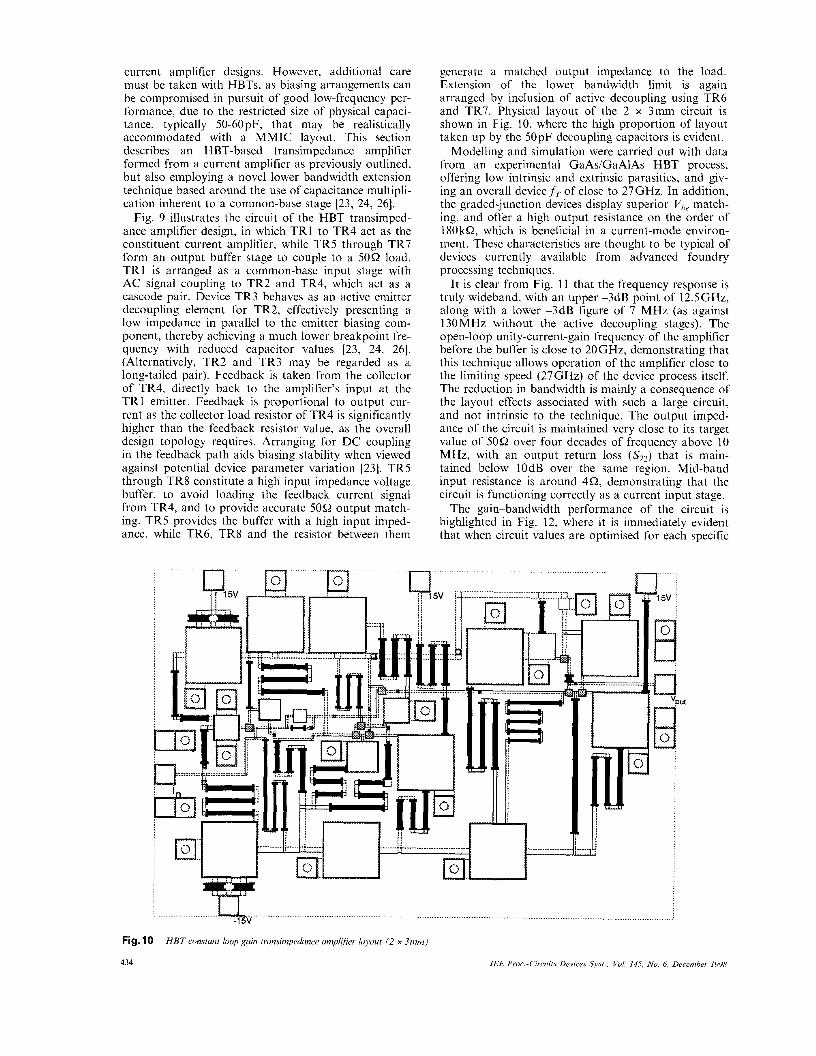
current amplifier designs. However, additional care must be taken with HBTs, as biasing arrangements can be compromised in pursuit of good low-frequency per- formance, due to the restricted size of physical capaci- tance, typically 50-60pF, that may be realistically accommodated with a MMIC layout. This section describes an HBT-based transimpedance amplifier formed from a current amplifier as previously outlined, but also employing a novel lower bandwidth extension technique based around the use of capacitance multipli- cation inherent to a common-base stage [23, 24, 261.
Fig. 9 illustrates the circuit of the HBT transimped- ance amplifier design, in which TRl to TR4 act as the constituent current amplifier, while TR5 through TR7 form an output buffer stage to couple to a 50Q load. TRl is arranged as a common-base input stage with AC signal coupling to TR2 and TR4, which act as a cascode pair. Device TR3 behaves as an active emitter decoupling element for TR2, effectively presenting a low impedance in parallel to the emitter biasing com- ponent, thereby achieving a much lower breakpoint fre- quency with reduced capacitor values [23, 24, 261. (Alternatively, TR2 and TR3 may be regarded as a long-tailed pair). Feedback is taken from the collector of TR4, directly back to the amplifier's input at the TRI emitter. Feedback is proportional to output cur- rent as the collector load resistor of TR4 is significantly higher than the feedback resistor value, as the overall design topology requires. Arranging for DC coupling in the feedback path aids biasing stability when viewed against potential device parameter variation [23]. TR5 through TR8 constitute a high input impedance voltage buffer, to avoid loading the feedback current signal from TR4, and to provide accurate 5052 output match- ing. TR5 provides the buffer with a high input imped- ance, while TR6, TR8 and the resistor between them
Fig.
434
generate a matched output impedance to the load. Extension of the lower bandwidth limit is again arranged by inclusion of active decoupling using TR6 and TR7. Physical layout of the 2 x 3mm circuit is shown in Fig. IO, where the high proportion of layout taken up by the 50pF decoupling capacitors is evident.
Modelling and simulation were carried out with data from an experimental GaAsiGaAlAs HBT process, offering low intrinsic and extrinsic parasitics, and giv- ing an overall device f r of close to 27GHz. In addition, the graded-junction devices display superior V,, match- ing, and offer a high output resistance on the order of 180k52, which is beneficial in a current-mode environ- ment. These characteristics are thought to be typical of devices currently available from advanced foundry processing techniques.
It is clear from Fig. 11 that the frequency response is truly wideband, with an upper -3dB point of 12.5GHz, along with a lower -3dB figure of 7 MHz (as against 130MHz without the active decoupling stages). The open-loop unity-current-gain frequency of the amplifier before the buffer is close to 20GHz, demonstrating that this technique allows operation of the amplifier close to the limiting speed (27GHz) of the device process itself. The reduction in bandwidth is mainly a consequence of the layout effects associated with such a large circuit, and not intrinsic to the technique. The output imped- ance of the circuit is maintained very close to its target value of 5052 over four decades of frequency above I O MHz, with an output return loss (S22) that is main- tained below lOdB over the same region. Mid-band input resistance is around 452, demonstrating that the circuit is functioning correctly as a current input stage.
The gain-bandwidth performance of the circuit is highlighted in Fig. 12, where it is immediately evident that when circuit values are optimised for each specific
1 15L
t
1. .............................. U - ......................................................................................................................................................................................................... -1 5v
10 HBT constant loop p i n trunsimpedunce cNnpliJier luyout ( 2 x 3")
frequency, Hz Trunsitnpedunce response of HBT unplijier Fig. 11
R,. = 5052
20
16
2 14- 0
n E- 12-
-!? 2 8 -
10-
6 - rz
gain, dB C2 Fig. 12 R, = 5052 (i) Constant bandwidth; (ii) HBT transimpedance amplifier; (iii) constant gain- bandwidth product
Vuriution of bandwidth us ufiinction qf guin level
20
16 l8 t
:: 0 0 0.2 0.4 0.6 0.8 1 1.2 1.4 1.6 1.8 2
source capacitance, pF Fig. 13 R,- = 508
Bundtcidth us u function of source cupucitunce
gain level, then the new topology displays complete gain-bandwidth independence over the region illus- trated. The minor variation when moving into the higher gain region can be attributed to the change in dominance between the compensation capacitor and other circuit parasitics. Fig. 13 illustrates that the upper -3dB frequency of the amplifier is only reduced to 5.9GHz when the source capacitance is increased to 2pF, a value that may be considered high at these operating speeds. Such freedom from source capaci- tance limitations is a significant feature of this particu- lar configuration, and promises near-optimum behaviour from lower-cost photodiodes fabricated to
less demanding physical arrangements. In addition, the amplifier’s gain levels are very close to their theoretical values, as shown by the low gain error values in Fig. 14. Even at a gain of 54dBS2, the amplifier exhib- its only a small gain error of 0.5dB, demonstrating both the suitability of HBT devices to this mode of operation, and the fact that constant loop-gain circuits of this nature can achieve close to theoretical perform- ance with practical gain-independent bandwidth in the microwave region.
-. 56r G
U m 54- e 52- ._
50- 0
U 5 48-
46- -E 44 - m +- 42-
2 40- U
._ E 0 38-
1 2 1.8
1.6
I .4 m
1.2 T- 1 :
0.8 ,z D
0.6
0.4
0.2
0 36 38 40 42 44 46 48 50 52 54 56
ideal transimpedance gain, dB !2 Fig. 14 R, = 5052
Guin clejkirion and error
5 Conclusions
This paper has examined the feedback mechanism responsible for restricting operating bandwidths at high gains for wideband transimpedance amplifiers, and has shown how this can be overcome by exploiting the ben- efits of constant loop-gain feedback around a current amplifying element, in the design of an optical receiver front-end transimpedance stage, to achieve gain-band- width independence. A generalised model has been pre- sented for the new topology, with simulation results indicating that bandwidths in the GHz region, approaching the unity-current-gain frequency of the amplifier itself, may be expected for amplifiers fabri- cated from existing semiconductor technologies. The model described also serves as a benchmark for assess- ing the suitability of any particular technology to exploit the desired theoretical response. Full layout foundry simulation of two different amplifier designs based on MESFET and HBT technology, respectively, has shown that the approach is indeed capable of achieving a -3dB bandwidth close to that of the con- stituent current amplifier’s f T , and exhibiting a band- width extending well into the microwave region, by avoiding the most significant bandwidth restriction imposed on previous configurations in this frequency region.
6 Acknowledgments
The authors wish to acknowledge the valuable contri- bution of I. Darwazeh to aspects of MMIC layout and performance simulation. In addition, suggestions by the anonymous reviewers have resulted in improvements to particular aspects of the paper’s coverage.
7 References
1 ALLEN, P.E., and TERRY, M.B.: ‘The use of current amplifiers for high-performance voltage applications’, ZEEE J . Solid-Srute Circuits, 1980, SC-17, pp. 155-162
435
WILSON, B.: ‘Performance analysis of current conveyors’, Elec- tron. Lett., 1989, 25, pp. 1596-1598 WILSON, B.: ‘Recent developments in current conveyors and current-mode circuits’, IEE Proc. G, 1990, 137, pp. 63-77 BOWERS, D.F., ALEXANDER, M., and BUXTON, J.: ‘A comprehensive simulation macromodel for current feedback oper- ational amplifiers’, IEE Proc. G, 1990, 137, pp. 137-145 MOI, T.V.: ‘Receiver design for high-speed optical fiber systems’, J . Lightwave Technol.. 1984, LT-3, pp. 243-267 OGAWA, K.: ‘Considerations for optical receiver design’, IEEE J. Sel. Areas Commurl., 1983, 3, pp. 524-532 WILSON, B., and DARWAZEH, I.: ‘Transimpedance optical preamplifier with a very low input resistance’, Electron. Lett.,
DARWAZEH, I., MOREIRA, P.M.R.S., LANE, P.M., and O’REILLY, J.J.: ‘A low input impedance multi-gigabit GaAs ootical receiver tolerant to ohotodiode Darasitics’. Presented at
1987, 23, pp. 88-89
IBEE international sqmposiim on MMI& in optical conimunica- tions, King’s College, London, Sept. 1992 VANISRI, T., and TOUMAZOU, C.: ‘On the design of low- noise optimisation of current-mode transimpedance optical preamplifiers’, Analog Integr. Circuits Signal Process., 1992, 2, pp. 179-1 95
I O HARROLD, S.J., JUDD, N.P., and WILSON, B.: ‘Integrated 4.8 Gb/s current-mode transimpedance optical preamplifier’. Paper 10, IEE Colloquium on Optical detectors and receivers, London, October 1993, Vol. Digest 1993/173
11 VANISRI, T., and TOUMAZOU, C.: ‘Integrated high-frequency low-noise current-mode optical transimpedance preamplifiers: theory and practice’, IEEE J . Solid-State Circuits, 1995, 30, pp.
12 TOUMAZOU, C., and PARK, S.M.: ‘Wideband low noise CMOS transimpedance amplifier for gigahertz operation’, Elec- tron. Lett., 1996, 32, pp. 11941 196
13 PARK, S.M., and TOUMAZOU, C.: ‘Gigahertz low-noise CMOS transimpedance amplifier’. Proceedings of IEEE interna- tional symposium on Circuits and systems, Hong Kong, 1997, Vol. 1, pp. 209-212
14 VANISRI, T., and TOUMAZOU, C.: ‘Low-noise optimisation of current-mode transimpedance optical preamplifiers’. Proceedings of IEEE international symposium on Circuits und systems, Chi- cago, 1993, Vol. 2, pp. 966969
15 VANISRI, T., and TOUMAZOU, C.: ‘Low-noise current-mode optical preamplifier’. Proceedings of IEEE international sympo- sium on Circuits and systems, San Diego, 1992, Vol. 3, pp. 2860- 2863
677-685
16 WILSON, B.: ‘Current-mode circuits: analysis and CAD model- ling’. Proceedings of IEEE international symposium on Circuits and systems, New Orleans, 1990, USA, Vol. 4, pp. 3242-3245
17 WILSON, B., and DREW, J.D.: ‘New current-mode transimped- ance amplifier for gain-independent bandwidth’. Paper 9, IEE Colloquium on Wideband circuits, modelling arid techniques, Lon- don, May 1996, Vol. Digest 199611 11
18 BRUUN, E.: ‘Bandwidth limitations in current-mode and volt- age-mode integrated feedback amplifiers’. Proceedings of IEEE international symposium on Circuits and systems, Seattle, USA, 1995, Vol. 1, pp. 303-306
19 PAYNE, A., and TOUMAZOU, C . : ‘Analog amplifiers: classifi- cation and generalisation’, IEEE Trans. Circuits Syst. I , Fundam. Theory Appl., 1996, 43, pp. 43-50
20 WILSON, B., and DREW, J.D.: ‘Transimpedance formulation exhibits gain-bandwidth independence at microwave frequencies’, Electron. Lett., 1997, 33, pp. 410411
21 WILSON, B., and DREW, J.D.: ‘Novel transimpedance amplifier formulation exhibiting gain-bandwidth independence’. Proceed- ings of IEEE international symposium on Circuits and systems, Hong Kong, 1997, Vol. 1, pp. 169-172
22 CHERRY, E.M.: ‘Input impedance and output impedance of feedback amplifiers’, IEE Proc. Circuits, Devices Syst., 1996, 143, pp. 195-201
23 DREW, J.D.: ‘Wideband current-mode amplifier structures’. PhD thesis, University of Manchester Institute of Science and Technol- ogy (UMIST), Manchester, UK, October 1996
24 DREW, J.D., DARWAZEH, I.Z., and WILSON, B.: ‘Genera- tion of negative capacitance in a common-gate MESFET stage and its application to optical receiver design at microwave fre- quencies’. Paper 2, IEE Colloquium on Wideband circuits. model- ling und techiizques, London, May 1996, Vol. Digest 1996/11 I ,
25 DARWAZEH, I.Z., MOREIRA, P.M.R.S., LANE, P.M., and O’REILLY, J.J.: ‘5 Gbit/s optical receiver MMIC’. Proceedings of 5th Bangor symposium on Communications, June 1993, Uni- versity of Wales, Bangor, UK, pp. 163-166
26 DREW, J.D., WILSON, B., and DARWAZEH, I.Z.: ‘New active decoupling technique extends lower bandwidth limit for HBT-based MMIC amplifiers’. Proceedings of 5th IEEE interna- tional workshop on High performance devices for microwave and optoelectronic upplicutions (EDMO 97), King’s College London, 24-25 November 1997, pp. 181-186