Page 1 of 6 High Power RF/Microwave Transistors, Pallets and Amplifiers from Integra Technologies, Inc. By Apet Bersegyan ABSTRACT Integra Technologies, Inc. is engaged in design and manufacturing of High Power RF/Microwave transistors, 50-ohm matched pallet amplifiers, miniaturized power amplifiers (MPA) and High Power Amplifiers (HPA) based on silicon Bipolar and FET technologies, including LDMOS, operating from VHF to S-band frequencies. Currently, extensive development work is being done on Gallium Nitride technology, which will enable operations for X-band and higher frequencies. Incorporated in the state of California in 1997, Integra has become a leading supplier of RF transmitter modules for Radar and Avionics equipment and system manufacturers. Today Integra is a multi-million dollar, ISO9001 certified company with a broad customer base spanning the globe including Armenia. The purpose of this paper is to familiarize the audience with the company and how its products can be used in Armenia. The 50 Ohm pallets are essentially building blocks combined in parallel to achieve any required system level power for a conventional high power transmitter or can be used individually as radiating elements for a Phased Array Radar ( PAR) system. Institutions in Armenia have been utilizing such products to build RF transmitters. This knowledge base which appears to be growing over the years can be extended to cover other types of RF transmitters used in Avionics, Broadcast, Cell phone infrastructure, SATCOM and miscellaneous wireless communication systems. The photo below illustrates an S-band 3.1-3.5GHz, 2-stage, 650 Watt HPA, where Integra transistors and pallets are employed on both stages of amplification. The unit also includes digital circuitry to monitor output Voltage Standing Wave Ratio (VSWR) and flange temperature of transistors. Systems designers use several such HPA’s combined in parallel to achieve desired system level power.
Transcript
Page 1 of 6
High Power RF/Microwave Transistors, Pallets and Amplifiers from Integra Technologies, Inc.
By Apet Bersegyan ABSTRACT Integra Technologies, Inc. is engaged in design and manufacturing of High Power RF/Microwave transistors, 50-ohm matched pallet amplifiers, miniaturized power amplifiers (MPA) and High Power Amplifiers (HPA) based on silicon Bipolar and FET technologies, including LDMOS, operating from VHF to S-band frequencies. Currently, extensive development work is being done on Gallium Nitride technology, which will enable operations for X-band and higher frequencies. Incorporated in the state of California in 1997, Integra has become a leading supplier of RF transmitter modules for Radar and Avionics equipment and system manufacturers. Today Integra is a multi-million dollar, ISO9001 certified company with a broad customer base spanning the globe including Armenia. The purpose of this paper is to familiarize the audience with the company and how its products can be used in Armenia. The 50 Ohm pallets are essentially building blocks combined in parallel to achieve any required system level power for a conventional high power transmitter or can be used individually as radiating elements for a Phased Array Radar ( PAR) system. Institutions in Armenia have been utilizing such products to build RF transmitters. This knowledge base which appears to be growing over the years can be extended to cover other types of RF transmitters used in Avionics, Broadcast, Cell phone infrastructure, SATCOM and miscellaneous wireless communication systems. The photo below illustrates an S-band 3.1-3.5GHz, 2-stage, 650 Watt HPA, where Integra transistors and pallets are employed on both stages of amplification. The unit also includes digital circuitry to monitor output Voltage Standing Wave Ratio (VSWR) and flange temperature of transistors. Systems designers use several such HPA’s combined in parallel to achieve desired system level power.
Page 2 of 6
Figure 1. 3.1-3.5GHz, 2-stage, 650 Watt Pulsed Power Amplifier
Page 3 of 6
1.1 IBA3135M650 Amplifier
The IBA3135M650 is a solid state, base plate cooled, pulsed RF amplifier operating in the 3.1-3.5GHz frequency range. Its operating voltage is 36.0 ± 0.2VDC and operating temperature is -25 to +65ºC. The amplifier has an optional internal circuitry to monitor temperature and operating power levels (input, output, and reflected). RF input to the amplifier is through a female SMA connector and output is via a female N connector. This amplifier is intended for use in military radar systems and is capable of a wide variety of pulse formats and duty cycles. Its output is protected against high VSWR by an internal circulator. The nominal output power at 25ºC is 650W with 25W input power.
1. Specifications @ 25 degree Celsius • Operating frequency range – 3.1 to 3.5GHz • Instantaneous Bandwidth – 400MHz • Output Power - > 650W peak • Input Power – 25W peak • Input Return Loss - > 10dB • Pulse Width – up to 150us • Duty Cycle – 10% max • Pulse Amplitude Droop – 1dB max • Insertion Phase – 0 ± 20º • Peak DC Current – 80A max • RF Envelope Rise time – 130ns max • RF Envelope Fall time – 110ns max • Spurious Outputs – 50dBc min • Harmonics (2nd through 4th) – 30dBc • Note: Amplifier can operate at higher duty cycles with reduced power output
1.2 Amplifier Architecture
The IBA3135M650 is a solid state two-stage pulsed power amplifier. The RF amplifier assembly consists of a hybrid coupled first stage driver module followed by a 4-way hybrid power splitter. The four outputs from the power splitter are fed to 4 identical hybrid coupled power modules whose outputs are combined and routed to the internal output circulator, protecting the module from high VSWR load conditions.
Page 4 of 6
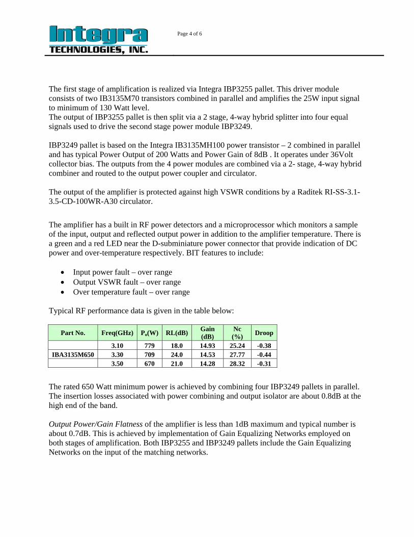
The first stage of amplification is realized via Integra IBP3255 pallet. This driver module consists of two IB3135M70 transistors combined in parallel and amplifies the 25W input signal to minimum of 130 Watt level. The output of IBP3255 pallet is then split via a 2 stage, 4-way hybrid splitter into four equal signals used to drive the second stage power module IBP3249. IBP3249 pallet is based on the Integra IB3135MH100 power transistor – 2 combined in parallel and has typical Power Output of 200 Watts and Power Gain of 8dB . It operates under 36Volt collector bias. The outputs from the 4 power modules are combined via a 2- stage, 4-way hybrid combiner and routed to the output power coupler and circulator. The output of the amplifier is protected against high VSWR conditions by a Raditek RI-SS-3.1-3.5-CD-100WR-A30 circulator.
The amplifier has a built in RF power detectors and a microprocessor which monitors a sample of the input, output and reflected output power in addition to the amplifier temperature. There is a green and a red LED near the D-subminiature power connector that provide indication of DC power and over-temperature respectively. BIT features to include:
• Input power fault – over range • Output VSWR fault – over range • Over temperature fault – over range
Typical RF performance data is given in the table below:
The rated 650 Watt minimum power is achieved by combining four IBP3249 pallets in parallel. The insertion losses associated with power combining and output isolator are about 0.8dB at the high end of the band. Output Power/Gain Flatness of the amplifier is less than 1dB maximum and typical number is about 0.7dB. This is achieved by implementation of Gain Equalizing Networks employed on both stages of amplification. Both IBP3255 and IBP3249 pallets include the Gain Equalizing Networks on the input of the matching networks.
Page 5 of 6
1.3 IBP3249 and IBP3255 pallet amplifiers
As we mentioned above, IBP3255 pallet consists of two IB3135M70 transistors combined in parallel. It operates under 36Volt collector bias and has typical Power Gain of 7.5dB. Typical RF data is given in the table below:
3.50 143 14.0 7.57 40.35 -0.19 IBP3249 pallet is based on the Integra IB3135MH100 power transistor, operates under 36Volt collector bias and has typical Power Output of 200 Watts and Power Gain of 8dB. Typical RF data is given in the table below:
The primary building block of a reliable High Power RF amplifier is the RF circuit and the High Power RF transistor itself. It is in the design of this transistor that reliability related factors, such as metallization and ballasting, must be taken into account. Integra’s transistors utilize high ft process, interdigitated geometry and gold metallization for the highest possible functional performance and reliability. Emitter ballast resistors assure devices are less susceptible to thermal runaway and prevent hot spotting across the transistor chip. Integra’s IB3135M70 transistor is used for the 1st stage of the amplifier. The second stage of amplification is realized via IB3135MH100 transistor. Both transistors are Common Base, Class C, hybrid bipolar junction transistors, are gold metallized and use gold bonding wires for electrical connections to enhance device reliability. IB3135MH100 device is specified at 100 Watt minimum output power over the given frequency with 7.90 dB minimal gain. The device has internal input and output matching networks and operates from a single 36V power supply. It is rated at 2:1 VSWR for survivability. IB3135M70 device is specified at 70 Watt minimum output power over the given frequency with 7.65 dB minimal gain. The device has internally matched input and output networks and operates from a single 36V power supply. The device is also rated at 2:1 VSWR for survivability.
Page 6 of 6
Conclusion
Integra Technologies, Inc is a vertically integrated company with unique ability to provide high
power RF solutions from basic transistors to pallet and amplifier levels, covering operations from
VHF to S-band frequencies. Over the past several years Integra has proven many times its ability
to design and mass produce state of the art transistors, pallets and amplifiers in very short time
intervals. Integra products are used in critical systems such as Air Traffic Control, Phased Array,
Shipboard and other military and civilian use radars. Therefore, regardless of your needs in RF
High Power industry – transistors, pallets or amplifiers, Integra Technologies, Inc is able and
willing to help you to find and produce solutions. If you have a system level requirement, for
example, transmitter box or complete radar system, Integra team can help you to select right
component from the existing reach portfolio or if necessary, will develop one that will work for
you. We will work with you to create component specifications based on the given system level
requirement and support your needs through production cycle.
1kW GaN S Band Radar Transistor
John Walker, Gabriele Formicone, Fouad Boueri, Brian Battaglia
Abstract—This paper describes a GaN transistor with 1kW
output power for S band radar and other applications. This is
believed to be the highest power ever reported from a single-
ended transistor at this frequency and is a threefold
improvement on the previous best.
Keywords—GaN; transistor; S band; radar
I. INTRODUCTION
Silicon bipolar transistors for S band radar have been available for many years and will continue to be available for many years to come. This technology is proven, highly reliable, and offers high efficiency due to the use of class C bias, typically around 50%. Furthermore, bipolar transistors have the simplest form of DC bias networks of any transistor technology at this frequency range and use the least number of additional components on the RF circuit board. However, the technology has three distinct disadvantages, namely low RF gain (typically around 9dB for the highest power parts), high output capacitance per Watt which imposes a power/bandwidth limit on the technology, and the need for an insulating material in the package, typically BeO but sometimes AlN. The low RF gain is a result of using emitter ballast resistors. These are required to prevent thermal run-away but they also provide negative feedback which lowers the intrinsic gain of the transistor. An example of a typical state of the art product is IB2729M170 [1] which delivers typically a minimum pulsed output power of 190W over 2.7-2.9GHz with 45% power-added efficiency and >9dB gain.
More recently, LDMOS has been developed for S band radar applications. The main advantage of LDMOS is that it uses a non-insulating package which doesn’t require an environmentally unfriendly material such as BeO. It also offers slightly higher gain, typically 2dB more for the same output power as a bipolar equivalent, but the maximum output power is about the same for the two technologies. LDMOS devices are typically designed for Class A/B operation which has worse efficiency than Class C (typically 5% less), and the MOSFET device requires additional DC bias circuitry to suppress the low frequency oscillations coming from the bias networks. In order to design a RF test circuit that is free from spurious oscillations both the gate and the drain terminals need many external components such as ferrite beads and an array of decoupling capacitors on the DC bias feeds from the DC power supplies.
In summary, LDMOS hasn’t provided the radar designer with a huge leap forward in performance. Due to the frequency limitations of silicon technology there is little prospect of any future significant improvement in either bipolar or LDMOS performance at S band. An example of a typical state of the art LDMOS transistor is ILD2731M140 [2] which delivers typically a minimum pulsed output power of 180W over 2.7-3.1GHz with 40.5% power-added efficiency and >10dB gain.
GaN transistors, on the other hand, offer a quantum leap forward in performance. GaN is a wide band-gap semiconductor and this enables the use of a much higher supply voltage (50V versus 32V for LDMOS) which, in turn, results in much higher power density. The high power density provides lower capacitance per Watt which enables higher power parts to be produced for the same bandwidth. The higher supply voltage also means that the load resistance is higher for the same output power which results in higher efficiency and easier circuit design. However, the higher power density creates heat dissipation problems which are a serious issue for CW parts but which makes GaN an ideal technology for high power pulsed applications. Table 1 summarizes the typical performance of 2.7-2.9GHz transistors designed for 10% duty
cycle 300µs pulse lengths with broadly similar output power. The GaN device in this case is operated at a similar supply voltage rather than one to maximize power, efficiency and gain.
TABLE I. TRANSISTOR COMPARISON
Device
Parameter
Technology Power
(W)
Power-Added
Efficiency
%
Gain
(dB)
Voltage
(V)
IB2729M170 Si Bipolar 190 45 9.5 36
ILD2731M140 LDMOS 180 40.5 10.5 32
IGN2729M250
[3] GaN 260 51 9.5 36
In 2011 Kwack et al [4] reported a 1kW amplifier for 2.9-3.3GHz radar applications that combined 8 approximately 150W GaN transistors to achieve the 1kW output power. The
output stage occupies an area of around 160 cm2 after
subtracting the area occupied by the 4 isolators. In this paper a single GaN transistor is reported that delivers 1kW peak at center frequency of 2.8GHz with a minimum of 56% power-added efficiency and 10dB gain. This removes the need to use a total of 10 Wilkinson power combiners, and the total circuit area is 32 cm
2 - less than 1/5
th of that required by Kwack et al.
To the best of the authors’ knowledge this represents the highest power achieved from a transistor at this frequency and sets a new bench-mark for solid-state in terms of the overall combination of power, gain and efficiency.
II. TRANSISTOR DESIGN AND PERFORMANCE
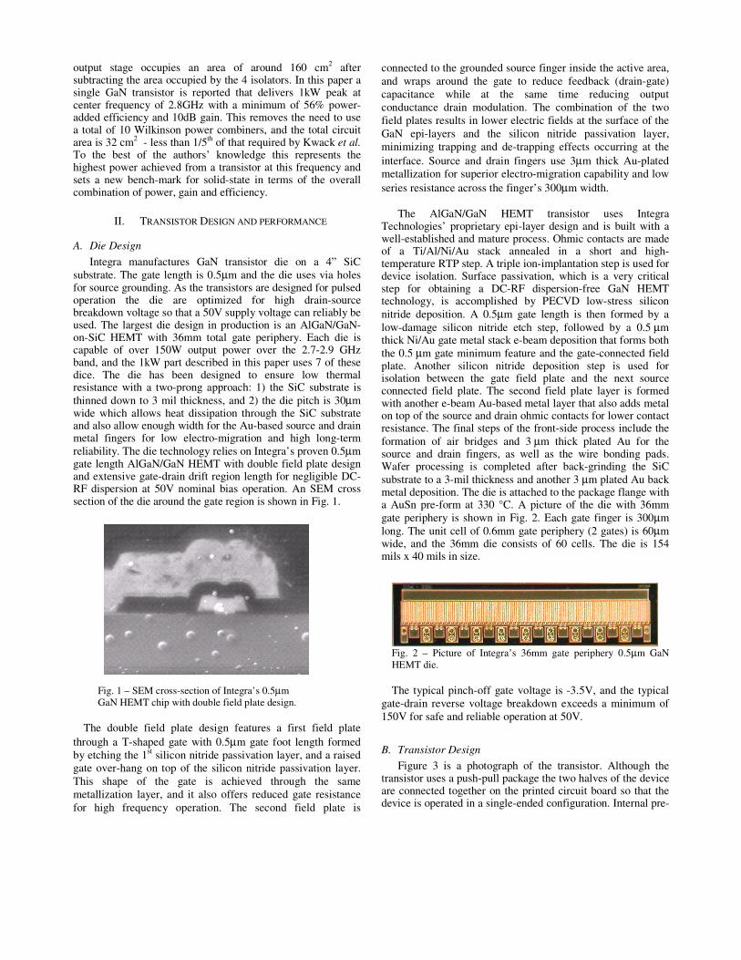
A. Die Design
Integra manufactures GaN transistor die on a 4” SiC
substrate. The gate length is 0.5µm and the die uses via holes for source grounding. As the transistors are designed for pulsed operation the die are optimized for high drain-source breakdown voltage so that a 50V supply voltage can reliably be used. The largest die design in production is an AlGaN/GaN-on-SiC HEMT with 36mm total gate periphery. Each die is capable of over 150W output power over the 2.7-2.9 GHz band, and the 1kW part described in this paper uses 7 of these dice. The die has been designed to ensure low thermal resistance with a two-prong approach: 1) the SiC substrate is
thinned down to 3 mil thickness, and 2) the die pitch is 30µm wide which allows heat dissipation through the SiC substrate and also allow enough width for the Au-based source and drain metal fingers for low electro-migration and high long-term
reliability. The die technology relies on Integra’s proven 0.5µm gate length AlGaN/GaN HEMT with double field plate design and extensive gate-drain drift region length for negligible DC-RF dispersion at 50V nominal bias operation. An SEM cross section of the die around the gate region is shown in Fig. 1.
Fig. 1 – SEM cross-section of Integra’s 0.5µm
GaN HEMT chip with double field plate design.
The double field plate design features a first field plate
through a Τ-shaped gate with 0.5µm gate foot length formed
by etching the 1st silicon nitride passivation layer, and a raised
gate over-hang on top of the silicon nitride passivation layer.
This shape of the gate is achieved through the same
metallization layer, and it also offers reduced gate resistance
for high frequency operation. The second field plate is
connected to the grounded source finger inside the active area,
and wraps around the gate to reduce feedback (drain-gate)
capacitance while at the same time reducing output
conductance drain modulation. The combination of the two
field plates results in lower electric fields at the surface of the
GaN epi-layers and the silicon nitride passivation layer,
minimizing trapping and de-trapping effects occurring at the
interface. Source and drain fingers use 3µm thick Au-plated
metallization for superior electro-migration capability and low
series resistance across the finger’s 300µm width.
The AlGaN/GaN HEMT transistor uses Integra
Technologies’ proprietary epi-layer design and is built with a well-established and mature process. Ohmic contacts are made of a Ti/Al/Ni/Au stack annealed in a short and high-temperature RTP step. A triple ion-implantation step is used for device isolation. Surface passivation, which is a very critical step for obtaining a DC-RF dispersion-free GaN HEMT technology, is accomplished by PECVD low-stress silicon
nitride deposition. A 0.5µm gate length is then formed by a
low-damage silicon nitride etch step, followed by a 0.5 µm thick Ni/Au gate metal stack e-beam deposition that forms both
the 0.5 µm gate minimum feature and the gate-connected field plate. Another silicon nitride deposition step is used for isolation between the gate field plate and the next source connected field plate. The second field plate layer is formed with another e-beam Au-based metal layer that also adds metal on top of the source and drain ohmic contacts for lower contact resistance. The final steps of the front-side process include the
formation of air bridges and 3 µm thick plated Au for the source and drain fingers, as well as the wire bonding pads. Wafer processing is completed after back-grinding the SiC
substrate to a 3-mil thickness and another 3 µm plated Au back metal deposition. The die is attached to the package flange with a AuSn pre-form at 330 °C. A picture of the die with 36mm
gate periphery is shown in Fig. 2. Each gate finger is 300µm
long. The unit cell of 0.6mm gate periphery (2 gates) is 60µm wide, and the 36mm die consists of 60 cells. The die is 154 mils x 40 mils in size.
Fig. 2 – Picture of Integra’s 36mm gate periphery 0.5µm GaN
HEMT die.
The typical pinch-off gate voltage is -3.5V, and the typical
gate-drain reverse voltage breakdown exceeds a minimum of
150V for safe and reliable operation at 50V.
B. Transistor Design
Figure 3 is a photograph of the transistor. Although the transistor uses a push-pull package the two halves of the device are connected together on the printed circuit board so that the device is operated in a single-ended configuration. Internal pre-
matching is used within the package and Table 2 shows how effective this is in raising the impedance to a manageable level even though this is a 1kW transistor. The corresponding impedance values for a 1kW 1030MHz spot frequency LDMOS transistor are also shown as well to demonstrate how beneficial the lower capacitance per Watt of GaN is in keeping the impedance higher and this equates to less loss in the output matching network and hence higher efficiency.
Fig. 3 – Picture of 1kW pulsed transistor
TABLE II. TRANSISTOR OPTIMUM SOURCE AND LOAD IMPEDANCES
Device
Parameter
Frequency
(GHz)
ZSopt
(ΩΩΩΩ)
ZLopt
(ΩΩΩΩ)
IGN2729M800
2.7 1.6 + j2.2 1.4 – j3.1
2.8 1.6 + j2.4 1.5 + j3.9
2.9 1.8 + j2.7 2.8 + j6.2
ILD1011M1000HV 1.03 0.86 + j0.34 0.30 + j0.40
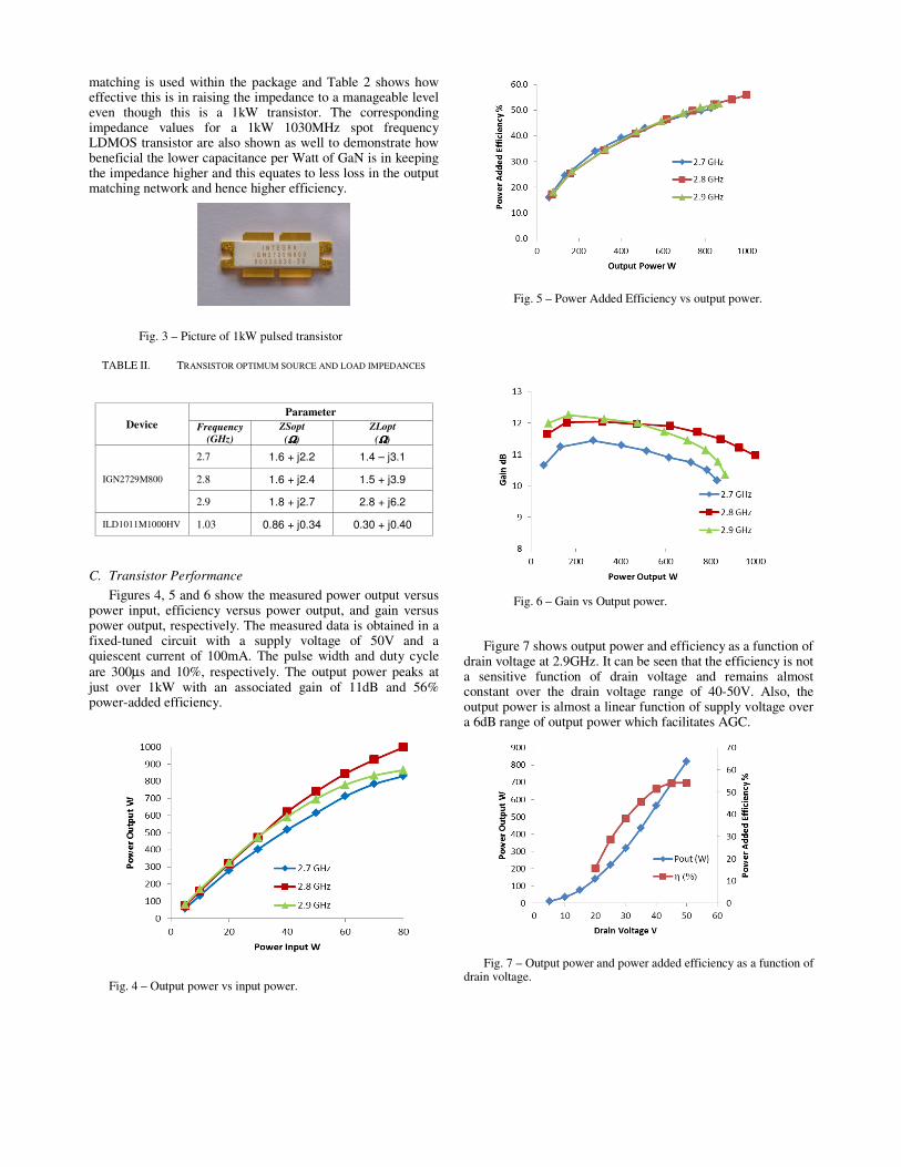
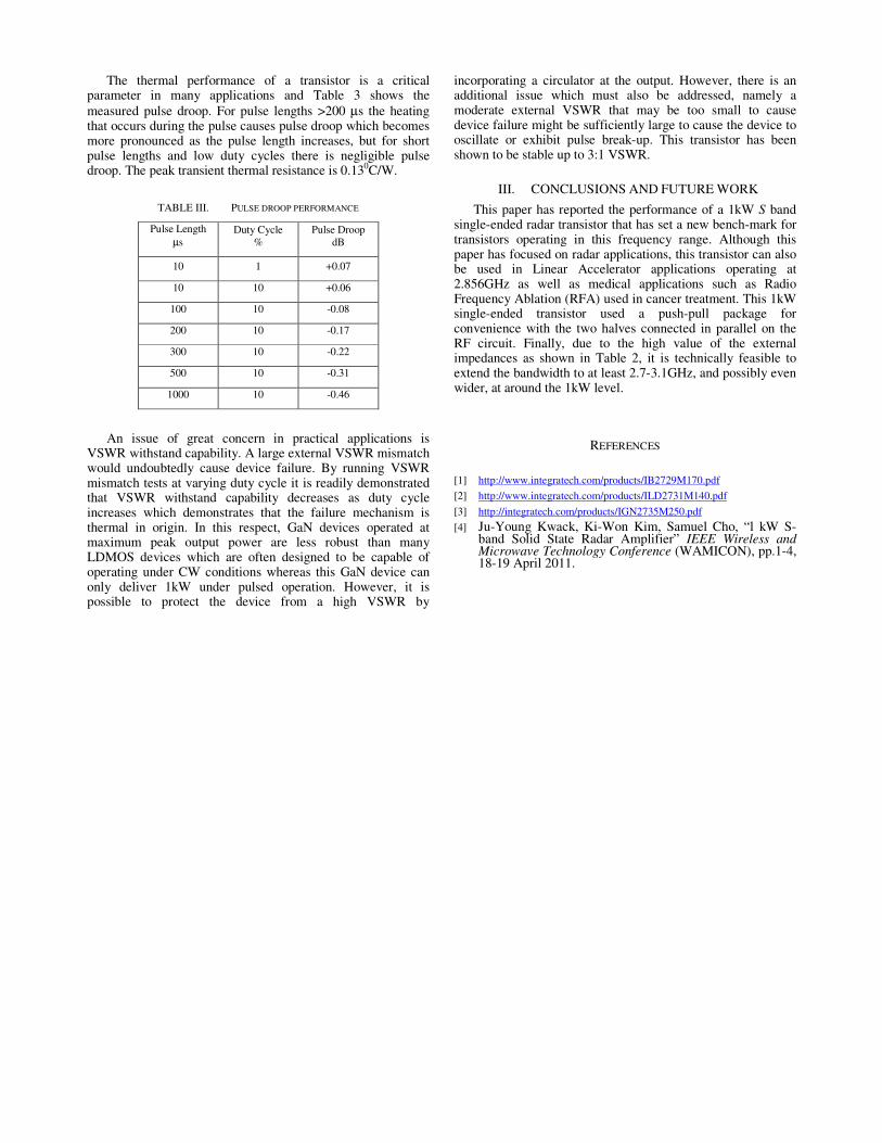
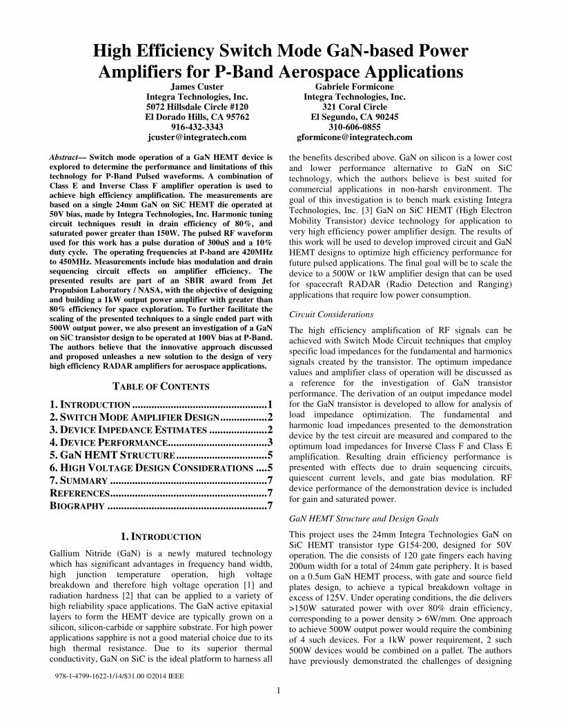
C. Transistor Performance
Figures 4, 5 and 6 show the measured power output versus power input, efficiency versus power output, and gain versus power output, respectively. The measured data is obtained in a fixed-tuned circuit with a supply voltage of 50V and a quiescent current of 100mA. The pulse width and duty cycle
are 300µs and 10%, respectively. The output power peaks at just over 1kW with an associated gain of 11dB and 56% power-added efficiency.
Fig. 4 – Output power vs input power.
Fig. 5 – Power Added Efficiency vs output power.
Fig. 6 – Gain vs Output power.
Figure 7 shows output power and efficiency as a function of drain voltage at 2.9GHz. It can be seen that the efficiency is not a sensitive function of drain voltage and remains almost constant over the drain voltage range of 40-50V. Also, the output power is almost a linear function of supply voltage over a 6dB range of output power which facilitates AGC.
Fig. 7 – Output power and power added efficiency as a function of drain voltage.
The thermal performance of a transistor is a critical parameter in many applications and Table 3 shows the
measured pulse droop. For pulse lengths >200 µs the heating that occurs during the pulse causes pulse droop which becomes more pronounced as the pulse length increases, but for short pulse lengths and low duty cycles there is negligible pulse droop. The peak transient thermal resistance is 0.130C/W.
TABLE III. PULSE DROOP PERFORMANCE
Pulse Length
µs
Duty Cycle
%
Pulse Droop
dB
10 1 +0.07
10 10 +0.06
100 10 -0.08
200 10 -0.17
300 10 -0.22
500 10 -0.31
1000 10 -0.46
An issue of great concern in practical applications is VSWR withstand capability. A large external VSWR mismatch would undoubtedly cause device failure. By running VSWR mismatch tests at varying duty cycle it is readily demonstrated that VSWR withstand capability decreases as duty cycle increases which demonstrates that the failure mechanism is thermal in origin. In this respect, GaN devices operated at maximum peak output power are less robust than many LDMOS devices which are often designed to be capable of operating under CW conditions whereas this GaN device can only deliver 1kW under pulsed operation. However, it is possible to protect the device from a high VSWR by
incorporating a circulator at the output. However, there is an additional issue which must also be addressed, namely a moderate external VSWR that may be too small to cause device failure might be sufficiently large to cause the device to oscillate or exhibit pulse break-up. This transistor has been shown to be stable up to 3:1 VSWR.
III. CONCLUSIONS AND FUTURE WORK
This paper has reported the performance of a 1kW S band single-ended radar transistor that has set a new bench-mark for transistors operating in this frequency range. Although this paper has focused on radar applications, this transistor can also be used in Linear Accelerator applications operating at 2.856GHz as well as medical applications such as Radio Frequency Ablation (RFA) used in cancer treatment. This 1kW single-ended transistor used a push-pull package for convenience with the two halves connected in parallel on the RF circuit. Finally, due to the high value of the external impedances as shown in Table 2, it is technically feasible to extend the bandwidth to at least 2.7-3.1GHz, and possibly even wider, at around the 1kW level.
[4] Ju-Young Kwack, Ki-Won Kim, Samuel Cho, “l kW S-band Solid State Radar Amplifier” IEEE Wireless and Microwave Technology Conference (WAMICON), pp.1-4, 18-19 April 2011.
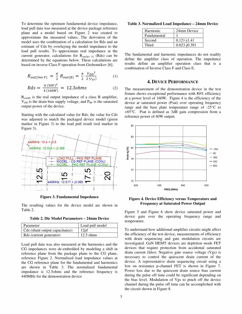
12.7 GHz). High cutoff frequency Ft is a requirement for
being able to implement harmonic tuning techniques and
achieve high efficiency power amplification. The maximum
current (IMAX) at Vgs = +1V is around ~0.8A/mm. At 50V
bias (VDD), with a ~10V saturated voltage (VSAT), the
maximum power density (PDMAX) is:
$%&' = (()*+),*-
(3)
PD012,4 = 54-47.81/::
= 8W/mm (4)
Figure 11. TCAD generated Ids-Vds curves showing
BVDSS in excess of 125V. The data are for a transistor
cell of 1mm in gate periphery. I-V curves are for VGS =
+1V (top), 0V, -1V -2V, -3V and -4V (bottom).
To understand thermal stress on the 24mm transistor die at
this power density, channel temperature can be considered.
Several techniques to compute the die thermal resistance
have been summarized by H. F. Cooke in Chapter 5 of
reference [7]. The thermal resistance (>?@) for the 24mm die
is calculated to be ~1.0°C/W, which accounts for the bare
GaN on SiC die, AuSn solder, and package flange. The
approximate peak channel temperature (Tchannel) can be
calculated by:
A@BCDE = ACFDGECD + >?@(IJ − L) (5)
IJ = MNOP
(6)
PDC is the input DC power to the device, PRF is the RF
power presented to the load, and η is the drain efficiency of
the amplifier. With 160W RF output power and 80% drain
efficiency the DC power is 200W. Therefore the dissipated
power PDC – PRF is 40W. For a base plate temperature of
85°C, the calculated peak junction temperature is 125°C.
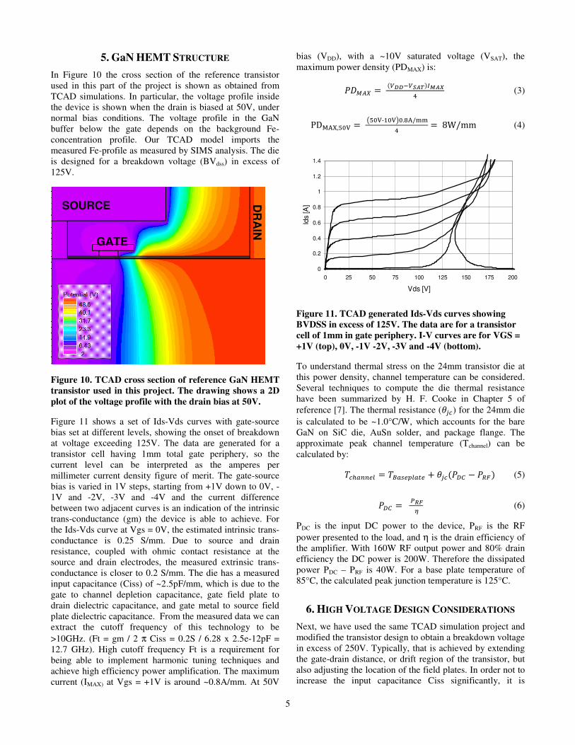
6. HIGH VOLTAGE DESIGN CONSIDERATIONS
Next, we have used the same TCAD simulation project and
modified the transistor design to obtain a breakdown voltage
in excess of 250V. Typically, that is achieved by extending
the gate-drain distance, or drift region of the transistor, but
also adjusting the location of the field plates. In order not to
increase the input capacitance Ciss significantly, it is
SOURCE
DR
AIN
GATE
SOURCE
DR
AIN
GATE
0
0.2
0.4
0.6
0.8
1
1.2
1.4
0 25 50 75 100 125 150 175 200
Vds [V]
Ids [A
]
6
important to keep the gate electrode structure unchanged as
much as possible; hence most of the field plates re-design is
focused around the source connected field plate. Further
improvements to the transistor design address the epi
design, which translate into a slightly increased epi
resistivity. A process split implemented when ordering the
modified epi and when manufacturing the new device may
result in further improvements to the data predicted with the
TCAD simulator. In Figure 12 the cross section of the
proposed transistor for a future phase of the project is shown
as obtained from TCAD simulations. The die is designed for
a breakdown voltage in excess of 250V. In particular, the
voltage profile inside the device is shown when the drain is
biased at 100V, under normal bias conditions.
Figure 12. TCAD cross section of high voltage proposed
GaN transistor design for next phase in this project. The
drawing shows a 2D plot of the voltage profile with the
drain bias at 100V.
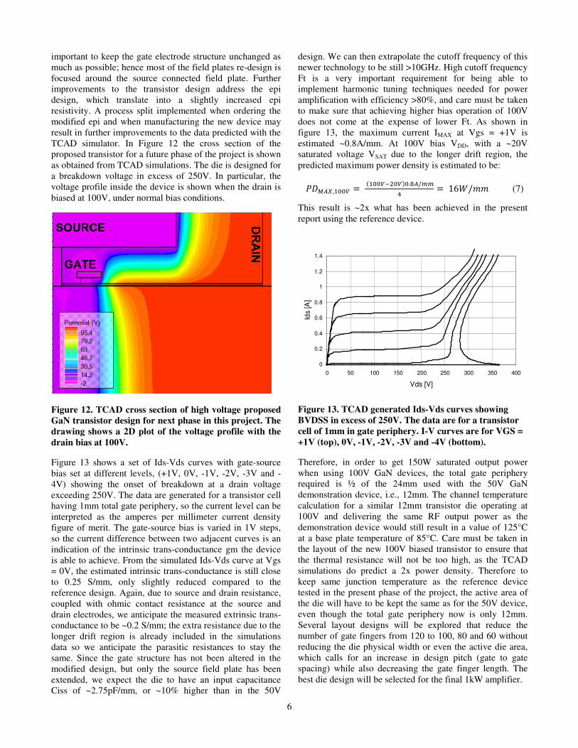
Figure 13 shows a set of Ids-Vds curves with gate-source
bias set at different levels, (+1V, 0V, -1V, -2V, -3V and -
4V) showing the onset of breakdown at a drain voltage
exceeding 250V. The data are generated for a transistor cell
having 1mm total gate periphery, so the current level can be
interpreted as the amperes per millimeter current density
figure of merit. The gate-source bias is varied in 1V steps,
so the current difference between two adjacent curves is an
indication of the intrinsic trans-conductance gm the device
is able to achieve. From the simulated Ids-Vds curve at Vgs
= 0V, the estimated intrinsic trans-conductance is still close
to 0.25 S/mm, only slightly reduced compared to the
reference design. Again, due to source and drain resistance,
coupled with ohmic contact resistance at the source and
drain electrodes, we anticipate the measured extrinsic trans-
conductance to be ~0.2 S/mm; the extra resistance due to the
longer drift region is already included in the simulations
data so we anticipate the parasitic resistances to stay the
same. Since the gate structure has not been altered in the
modified design, but only the source field plate has been
extended, we expect the die to have an input capacitance
Ciss of ~2.75pF/mm, or ~10% higher than in the 50V
design. We can then extrapolate the cutoff frequency of this
newer technology to be still >10GHz. High cutoff frequency
Ft is a very important requirement for being able to
implement harmonic tuning techniques needed for power
amplification with efficiency >80%, and care must be taken
to make sure that achieving higher bias operation of 100V
does not come at the expense of lower Ft. As shown in
figure 13, the maximum current IMAX at Vgs = +1V is
estimated ~0.8A/mm. At 100V bias VDD, with a ~20V
saturated voltage VSAT due to the longer drift region, the
predicted maximum power density is estimated to be:
$%&', = (().8&/QQ
= 16S/## (7)
This result is ~2x what has been achieved in the present
report using the reference device.
Figure 13. TCAD generated Ids-Vds curves showing
BVDSS in excess of 250V. The data are for a transistor
cell of 1mm in gate periphery. I-V curves are for VGS =
+1V (top), 0V, -1V, -2V, -3V and -4V (bottom).
Therefore, in order to get 150W saturated output power
when using 100V GaN devices, the total gate periphery
required is ½ of the 24mm used with the 50V GaN
demonstration device, i.e., 12mm. The channel temperature
calculation for a similar 12mm transistor die operating at
100V and delivering the same RF output power as the
demonstration device would still result in a value of 125°C
at a base plate temperature of 85°C. Care must be taken in
the layout of the new 100V biased transistor to ensure that
the thermal resistance will not be too high, as the TCAD
simulations do predict a 2x power density. Therefore to
keep same junction temperature as the reference device
tested in the present phase of the project, the active area of
the die will have to be kept the same as for the 50V device,
even though the total gate periphery now is only 12mm.
Several layout designs will be explored that reduce the
number of gate fingers from 120 to 100, 80 and 60 without
reducing the die physical width or even the active die area,
which calls for an increase in design pitch (gate to gate
spacing) while also decreasing the gate finger length. The
best die design will be selected for the final 1kW amplifier.
0
0.2
0.4
0.6
0.8
1
1.2
1.4
0 50 100 150 200 250 300 350 400
Vds [V]
Ids [A
]
7
A comparison of the key parameters for the existing 50V
and the proposed 100V GaN on SiC HEMT device is
summarized in Table 4.
Table 4. Comparison of key parameters for the 50V and
100V GaN on SiC HEMT Device
Parameter 50V Design 100V Design
BVdss [V] 125 250
VDD [V] 50 100
VSAT [V] 10 20
IMAX [A/mm] 0.8 0.8
PDMAX [W/mm] 8 16
Ciss [pF/mm] 2.5 2.75
gm [S/mm] 0.2 0.2
Ft [GHz] 12.7 11.6
7. SUMMARY
It has been shown that very high efficiency power
amplification at P-band is achievable with existing GaN on
SiC HEMT device technology from Integra Technologies,
Inc. The ultimate goal of this research is to enable very high
power and highly efficient amplifiers for P-Band, in excess
of 500W and greater than 80% efficiency. Scaling existing
50V technology to achieve greater than 500W will create
lower device impedances that will be more difficult to
match for high efficiency operation. Increasing the drain
voltage from 50V to 100V is an attractive option. The power
density (Watt/mm) increases by a factor of 2. For the same
RF output power the Cds decreases by a factor of 2 and the
Rds increases by a factor of 4. The reduction in Cds will
enable a larger range of harmonic tuning solutions for best
efficiency. TCAD simulations have shown that such a new
GaN device, operating at 100V bias, is indeed achievable.
REFERENCES
[1] Allen Katz, Marc Franco, ‘GaN Comes of Age,’ IEEE
Microwave Magazine, Vol.11, Issue 7, December 2011,
pp. S24-S34.
[2] R.D. Harris, L.Z. Scheick, J.P. Hoffman, T.
Thrivikraman, M. Jenabi, T. Miyahira, ‘Radiation
Characterization of Commercial GaN Devices,’ IEEE
Radiation Effects Data Workshop, July 2011, pp. 1-5.
[3] www.integratech.com
[4] J. Walker, G. Formicone, F. Boueri, B. Battaglia, ‘1kW
S band Radar Transistor,’ IEEE COMCAS 2013.
[5] Fredrick Raab, ‘Class-E, Class-C, and Class-F Power
Amplifiers Based upon a Finite Number of Harmonics,’
IEEE Transactions MTT, Vol. 49, no. 8, August 2001,
pp. 1462-1468.
[6] Andrei Grebennikov, Nathan Social, ‘Switch Mode RF
Power Amplifiers,’ Elsevier, Burlington, MA USA,
2007, pg. 164
[7] John L.B. Walker, “High Power Gas FET Amplifiers”,
Bartech House, USA, 1993.
BIOGRAPHY
James Custer received a B.S. in
Electrical and Electronic Engineering
from California State University,
Sacramento in 1980. He received an
M.S. in Electrical and Electronic
Engineering from California State
University, Sacramento in 1992. He has
worked as a design engineer, systems engineer and project
engineer in the high power amplifier field for over 25 years.
In September of 2011 he joined Integra Technologies, Inc.
to work on high power microwave GaN devices and
modules for radar and defense applications. Prior to
working at Integra, he worked at Avantek, Inc., Hewlett
Packard’s Wireless Infrastructure Division, and Powerwave
Technologies, Inc.
Dr. Gabriele F. Formicone received
his Ph. D. in Electrical Engineering
from Arizona State University. He has
over 15 years of hands-on industry
experience in the design of
RF/Microwave power transistors for
commercial linear applications in the
wireless infrastructure market and for military / defense
pulse applications in radar and avionics systems. His
industrial expertise covers Silicon Bipolar, Vertical and
Lateral DMOS transistors, and GaN HEMT RF power
technologies, spanning from TCAD simulations for
transistor design and process optimization, to transistor
layout, and project management with wafer fab and
foundry operations management.
Mixed-Mode Class E-F-1 High Efficiency GaN Power Amplifier for P-Band Space Applications
Gabriele Formicone and James Custer
Integra Technologies, Inc. 321 Coral Circle, El Segundo, CA 90245, USA
Abstract — A GaN based high efficiency, high power
amplifier in P-band for space borne radar applications is demonstrated. It uses a single chip transistor that achieves 250W output power with greater than 80% drain efficiency from 420MHz to 450MHz, using a pulsed waveform with 10% duty cycle. The circuit topology is based on a combination of class E and inverse class F harmonic tuning.
Index Terms — amplifier, class E, GaN, inverse class F, P-band, space, switch-mode, radar.
I. INTRODUCTION
Several space amplifier applications are adopting GaN technology due to the superior physical properties that this material offers. In reference [1] a 120W GaN amplifier module is reported with 60% efficiency for L-band SweepSAR radar systems. In reference [2] a comparison is made of class E, F and inverse F amplifiers in L-band (2 GHz) to determine the best performance achievable with a 10W GaN transistor targeted for satellite radio navigation (Galileo). In reference [3] the typical performance goals of output power, bandwidth and overall efficiency are outlined for a T/R module in L-band for future space needs.
Besides L-band, several space applications exist in P-band requiring high power and efficiency capabilities which have attracted significant development using GaN against other technologies: VDMOS/LDMOS are not radiation-hardened; GaAs uses low voltage, which adds high losses in power supply; bipolar has low gain; so that opens the door to GaN. Also, GaN has lowest output pF/W figure of merit which is an essential requirement for high efficiency switched amplifiers. For instance, Synthetic Aperture Radar (SAR) imaging of subsurface features for Mars, as suggested in reference [4], or other non-terrestrial objects, or the terrestrial surface itself, all benefit from power amplifiers based on GaN technology. Here, a high power amplifier in P-band would allow deeper ground penetration and subsurface imaging. Future interplanetary missions using Multi-Mission Subsurface Imaging Radar (MMSIR) technology would also benefit from a GaN based amplifier. An airborne test bed system for Biomass estimation (Airmoss) is in operation using P-Band SAR, which is the precursor to future space instruments [5]. With space operated radar instrumentation, it becomes mandatory matching the high output power requirements of an amplifier with high efficiency to keep power supply requirements and weight manageable, while at the same time
improving packaging and printed circuit board materials and techniques [6].
The purpose of the research work presented in this paper is to demonstrate a 250W GaN single transistor building block aimed at high power amplifier for P-Band radar applications such as space exploration and earth remote sensing, with efficiency targets above 80%. The power amplifier utilizes GaN HEMT device technology; we show results with GaN chips optimized to operate at 75V and 100V supply voltage, with impedance matching circuits that include harmonic tuning to optimize efficiency. The ultimate goal is to create an amplifier module with greater than 80% efficiency from 420MHz to 450MHz, using a pulsed waveform with 10% duty cycle. The objective has been achieved by implementing an impedance matching scheme that results in a combination of class E and inverse class F topology.
II. HIGH VOLTAGE GAN HEMT TECHNOLOGY
Our research work uses a GaN transistor built with a single chip to achieve a target of 250W minimum output power and 80% drain efficiency. Two different die configurations have been developed, with the following characteristics:
1) a 21mm die operating at 75V with 250W output power,
22dB gain and drain efficiency in excess of 80%; 2) a 15mm die operating at 100V with 250W output power,
25dB gain and drain efficiency in excess of 75%. The chip operating at 75V has a breakdown voltage in
excess of 200V, whereas the die designed to operate at 100V has a breakdown voltage exceeding 300V. Both chips versions are available with 0.5μm and 1μm gate length, whereas the main difference between the 75V and the 100V GaN HEMT devices is the length of the gate-drain extension (drift region) and the relative source connected field plate. The two different layout topologies were selected to address not only potential differences in thermal resistance and junction temperature, but also F/2 or harmonic spurious signals under mismatch and stability. The different die architectures also translate into different combining properties when building a transistor with two or more chips inside one package, targeting a 500W or higher output power level.
The test device uses an input LC resonance to increase the input gate impedance, and the drain is bonded directly to the transistor output lead to allow for fundamental and harmonic
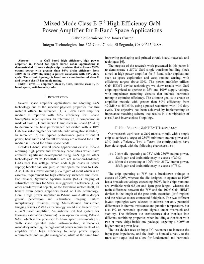
tuning outside the transistor package. The test environment used test fixtures with fixed tuned load impedances for all measurement frequencies with no external tuners. Separate test fixtures were created for each operating voltage and corresponding load line impedance. A picture of the package and internal device assembly is shown in Fig. 1.
Fig. 1. Package and internal assembly of GaN transistor.
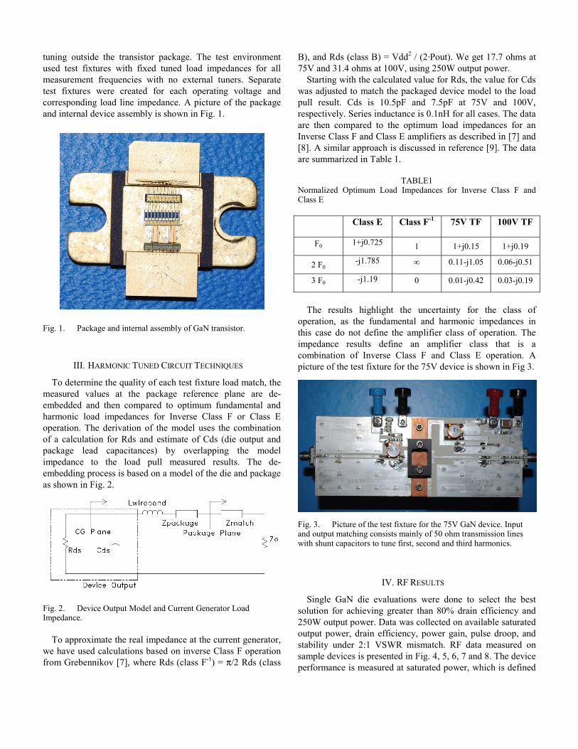
III. HARMONIC TUNED CIRCUIT TECHNIQUES
To determine the quality of each test fixture load match, the measured values at the package reference plane are de-embedded and then compared to optimum fundamental and harmonic load impedances for Inverse Class F or Class E operation. The derivation of the model uses the combination of a calculation for Rds and estimate of Cds (die output and package lead capacitances) by overlapping the model impedance to the load pull measured results. The de-embedding process is based on a model of the die and package as shown in Fig. 2. Fig. 2. Device Output Model and Current Generator Load Impedance.
To approximate the real impedance at the current generator,
we have used calculations based on inverse Class F operation from Grebennikov [7], where Rds (class F-1) = π/2 Rds (class
B), and Rds (class B) = Vdd2 / (2·Pout). We get 17.7 ohms at 75V and 31.4 ohms at 100V, using 250W output power.
Starting with the calculated value for Rds, the value for Cds was adjusted to match the packaged device model to the load pull result. Cds is 10.5pF and 7.5pF at 75V and 100V, respectively. Series inductance is 0.1nH for all cases. The data are then compared to the optimum load impedances for an Inverse Class F and Class E amplifiers as described in [7] and [8]. A similar approach is discussed in reference [9]. The data are summarized in Table 1.
TABLE1
Normalized Optimum Load Impedances for Inverse Class F and Class E
Class E Class F-1 75V TF 100V TF
F0 1+j0.725 1 1+j0.15 1+j0.19
2 F0 -j1.785 ∞ 0.11-j1.05 0.06-j0.51
3 F0 -j1.19 0 0.01-j0.42 0.03-j0.19
The results highlight the uncertainty for the class of
operation, as the fundamental and harmonic impedances in this case do not define the amplifier class of operation. The impedance results define an amplifier class that is a combination of Inverse Class F and Class E operation. A picture of the test fixture for the 75V device is shown in Fig 3. Fig. 3. Picture of the test fixture for the 75V GaN device. Input and output matching consists mainly of 50 ohm transmission lines with shunt capacitors to tune first, second and third harmonics.
IV. RF RESULTS
Single GaN die evaluations were done to select the best solution for achieving greater than 80% drain efficiency and 250W output power. Data was collected on available saturated output power, drain efficiency, power gain, pulse droop, and stability under 2:1 VSWR mismatch. RF data measured on sample devices is presented in Fig. 4, 5, 6, 7 and 8. The device performance is measured at saturated power, which is defined
at the point where the die is gain compressed enough to cause gate current to flow. This saturated power level is approximately 4dB to 5dB gain compression from a low output power reference, typically >10dB drive power below the saturation point.
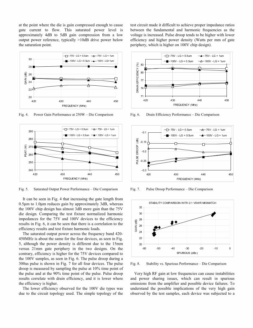
Fig. 4. Power Gain Performance at 250W – Die Comparison
Fig. 5. Saturated Output Power Performance – Die Comparison
It can be seen in Fig. 4 that increasing the gate length from
0.5μm to 1.0μm reduces gain by approximately 3dB, whereas the 100V chip design has almost 3dB more gain than the 75V die design. Comparing the test fixture normalized harmonic impedances for the 75V and 100V devices to the efficiency results in Fig. 6, it can be seen that there is a correlation to the efficiency results and test fixture harmonic loads.
The saturated output power across the frequency band 420-450MHz is about the same for the four devices, as seen in Fig. 5, although the power density is different due to the 15mm versus 21mm gate periphery in the two designs. On the contrary, efficiency is higher for the 75V devices compared to the 100V samples, as seen in Fig. 6. The pulse droop during a 300us pulse is shown in Fig. 7 for all four devices. The pulse droop is measured by sampling the pulse at 10% time point of the pulse and at the 90% time point of the pulse. Pulse droop results correlate with drain efficiency, and it is lower where the efficiency is higher.
The lower efficiency observed for the 100V die types was due to the circuit topology used. The simple topology of the
test circuit made it difficult to achieve proper impedance ratios between the fundamental and harmonic frequencies as the voltage is increased. Pulse droop tends to be higher with lower efficiency and higher power density (Watts per mm of gate periphery, which is higher on 100V chip design).
Fig. 6. Drain Efficiency Performance – Die Comparison
Fig. 7. Pulse Droop Performance – Die Comparison
Fig. 8. Stability vs. Spurious Performance – Die Comparison
Very high RF gain at low frequencies can cause instabilities and power sharing issues, which can result in spurious emissions from the amplifier and possible device failures. To understand the possible implications of the very high gain observed by the test samples, each device was subjected to a
20
22
24
26
28
30
420 430 440 450
FREQUENCY (MHz)
GA
IN (
dB)
75V - LG = 0.5um 75V - LG = 1um
100V - LG = 0.5um 100V - LG=1um
240
250
260
270
280
290
420 430 440 450FREQUENCY (MHz)
PSAT
(W
)
75V - LG = 0.5um 75V - LG = 1um
100V - LG = 0.5um 100V - LG = 1um
-0.3
-0.25
-0.2
-0.15
-0.1
420 430 440 450
FREQUENCY (MHz)
PULS
E D
RO
OP
(dB
)
75V - LG = 0.5um 75V - LG = 1um
100V - LG = 0.5um 100V - LG = 1um
71
74
77
80
83
420 430 440 450
FREQUENCY (MHz)
DR
AIN
EFF
ICIE
NC
Y (%
)
75V - LG = 0.5um 75V - LG = 1um
100V - LG = 0.5um 100V - LG = 1um
STABILITY COMPARISON WITH 2:1 VSWR MISMATCH
20
22
24
26
28
30
32
-60 -50 -40 -30 -20 -10 0
SPURIOUS (dBc)
GA
IN (d
B)
2:1 VSWR mismatch at the output with all phase angles. Fig. 8 shows a correlation between observed spurious under a 2:1 mismatch and the gain of the device at rated power. Although all chip types show the capability to achieve 250W and high efficiency, our results indicate that the best die selection moving forward for a multi-chip device design will be the 75V, 1μm gate length, 21mm gate periphery die. This device has the required saturated output power capability and the lowest gain to help mitigate low frequency instability issues.
The thermal resistance of the 15mm 100V devices has been calculated, as described in reference [10], to be 0.36 °C/W for the bare die, whereas for the 21mm 75V devices it is 0.31 °C/W. We have used a value of 300 W/m-°K for the thermal conductivity of the SiC substrate. The thermal resistance component for the package CPC flange is ~0.1 °C/W in both cases. Therefore the total thermal resistance of the 100V devices tested is 0.46 °C/W, and for the 75V devices it is 0.41 °C/W. At 420MHz, the 100V sample with 0.5μm gate length has 270W output power and 75% drain efficiency; therefore the DC power is 360W, and the dissipated power is 360W-270W=90W. For a base-plate temperature of 35 °C under forced air cooling, the calculated peak channel temperature is 76.4 °C which is very good from a reliability standpoint. A similar calculation at 420MHz for the 75V 1.0μm gate length device has 270W saturated output power and 81% drain efficiency; therefore the DC power is 333W, and the dissipated power is 333W-270W=63W. For a base-plate temperature of 35 °C under forced air cooling, the calculated peak channel temperature is now 60.8 °C which is also very good from a reliability standpoint. A more accurate analysis of the junction temperature has to account for the 300us pulse length with a 10% duty cycle. Time-domain simulations of the junction temperature under the specified pulse conditions have been carried out and the results are shown in Fig. 9.
Fig. 9. Junction temperature versus time for the 75V and 100V samples with 63W and 90W dissipated power, respectively. The data for the 100V chip are shifted by 1.5ms to facilitate the viewing of the junction temperature peaks.
Junction temperature on the 75V device barely reaches 60
°C, whereas on the 100V device it approaches 75°C, in good agreement with the projections made above. Gate length has
only minor effect on the junction temperature. Notice how the more efficient 75V devices operate at lower peak junction temperatures compared to the 100V devices, which translates into better reliability.
V. CONCLUSION
Several single GaN chip transistors have been evaluated for a 250W output power, 80% efficiency amplifier at P-band for radar applications in space exploration and earth remote sensing. The results are obtained with a circuit topology where the measured impedances are typical of a combination between class E and inverse class F power amplification. It has been demonstrated stable operation at 75V and 100V bias of a 250W power amplifier with greater than 80% efficiency and estimated junction temperature well below the 150 °C level needed for high reliability operation.
ACKNOWLEDGEMENT
The authors would like to thank Dr. John Walker, Lyle Leverich, Richard Keshishian, Jeff Burger and Brian Battaglia for reviewing and help improve the quality of the manuscript. In particular, the authors would like to thank Lyle Leverich for running the thermal simulations reported in Fig. 9.
REFERENCES
[1] T. Thrivikraman, S. Horst, D. Price, J. Hoffman and L. Veilleux, “A Compact Two-stage 120W GaN High Power Amplifier for SweepSAR Radar Systems,” 2014 IEEE Aerospace Conference, March 2014.
[2] A. Ramadan, A. Martin, D. Sardin, T. Reveyrand, J-M. Nebus, P. Bouyesse, L. Lapierre, J. F. Villemazet and S. Forestier, “Study and Design of High Efficiency Switch Mode GaN Power Amplifiers at L-band Frequency,” Advances in Computational Tools for Engineering Applications, 2009. ACTEA '09.
[3] W. N. Edelstein, C. Andricos, S. Madsen, F. Wang and D. B. Rutledge, “Current Status of the High-Efficiency L-band Transmit/Receive Module Development for SAR System”, Earth Science Technology Conference, June 2003.
[4] K. K. Williams and R. Greely, “Radar Imaging of Subsurface Geology through Sand: Analysis of Penetration Depth Variables With Implications For MARS Exploration”, Lunar and Planetary Science XXXI, p. 1023
[5] http://airmoss.jpl.nasa.gov [6] J. P. Hoffman, L. D. Castillo, J. Miller, M. Jenabi and G. Birur,
“Advanced packaging materials and techniques for high power T/R module”, Earth Science Technology Forum, 2011.
[7] Andrei Grebennikov, Nathan Sokal, “Switch Mode RF Power Amplifiers,” Elsevier, Burlington MA USA, pg. 160, 2007.
[8] F. Raab, “Class-E. Class-C, and Class F Power Amplifiers Based upon a Finite Number of Harmonics,” IEEE Transactions on Microwave Theory and Techniques, Vol. 49, No. 9, August 2001, pp 1462-1468.
[9] James Custer, Gabriele Formicone, ‘High Efficiency Switch Mode GaN-based Power Amplifiers for P-Band Aerospace Applications,’ 2014 IEEE Aerospace Conference, March 2014.
[10] John L. B. Walker, “High-Power GaAs FET Amplifiers,” Arthech House., 1993, p.234.
3035404550556065707580
0 0.005 0.01 0.015 0.02Time [sec.]
Junc
tion
Tem
pera
ture
[deg
C]
75V sample 100V sample
FOR RELEASE MAY 19, 2015
Integra Announces New High-Voltage GaN Transistors
Phoenix, AZ (USA) – May 19, 2015 – Integra Technologies, Inc. (ITI), a leading
manufacturer of high-power pulsed RF transistors, pallets and amplifiers, today
announces the development of a range of High-Voltage GaN on SiC transistors for sub-
1GHz applications.
Taking advantage of the intrinsically high power-density advantage of GaN on SiC,
Integra has developed a range of GaN on SiC devices that can operate from drain supply
voltages of 75V or more. Characterized in the P-band over 420-450MHz these devices
achieve efficiencies in excess of 80% with stable gain upwards of 27dB and more than
250W output power in a switched-mode circuit. This technology is ideally suited for
foliage penetration and ground penetration terrestrial or space-based radar systems. Paul
Akian, President of Integra Technologies, commenting on this development notes: “This
innovative development opens up new market opportunities for GaN in areas such as
Space-born radar, linear accelerators and other ISM applications”. Integra has published
performance data with breakdown voltages exceeding 600V enabling operating voltages
of 150V as we continue to push the performance of the technology.
Samples and Availability
For samples or to discuss your requirements for high-voltage GaN transistors please
1 Background Integra devices with the IGNxxxx part number nomenclature are discrete high power devices which utilize GaN on SiC HEMT technology. A GaN transistor is a depletion mode device, hence it requires a negative Gate voltage and a positive Drain supply voltage. The negative Gate voltage is required in order to pinch-off the Drain. An external Gate bias supply must be provided to apply the negative voltage to the Gate for setting IDQ. Integra E-K’s (evaluation kits) typically include two transistors and one RF test fixture. One of the transistors is shipped in place in the RF test fixture and supplied with RF test data in order to allow high power RF correlation testing. Drain supply charge storage is typically supplied by a 4700uF, 50V electrolytic capacitor.
2 Transistor Biasing and Turn-on Sequence The following sequence should be followed when turning on the transistor.
1. The transistor is sensitive to ESD, and should be handled and tested in an ESD protected environment.
2. Make sure that the RF is turned off before installing the test fixture. Make sure that the proper pulse width and duty cycle has been properly set on the RF source prior to turning on the transistor. The transistor may be damaged if the RF source is not putting out the correct pulse format.
3. Hookup the test fixture to a test bench with a good 50 ohm load on both the input and the output side RF connectors. The output must have a high power load capable of handling ~3dB more than both the rated peak output power and the average output power. The test set Return Loss at the RF test fixture connectors (input and output) should be at least 26dB for testing purposes. For accurate correlation the test set Return Loss is recommend to be 30dB minimum.
REFERENCE NUMBER Type IGNxxxx App Note 3/5/2013
AUTHOR IInntteeggrraa TECHNOLOGIES, INC. Jeff Burger Page 2 of 6
4. Check the screw torque on the transistor clamp to ensure that the clamp
has not loosened during shipment. The screws should be torqued sequentially to between 6-8 in/lbs.
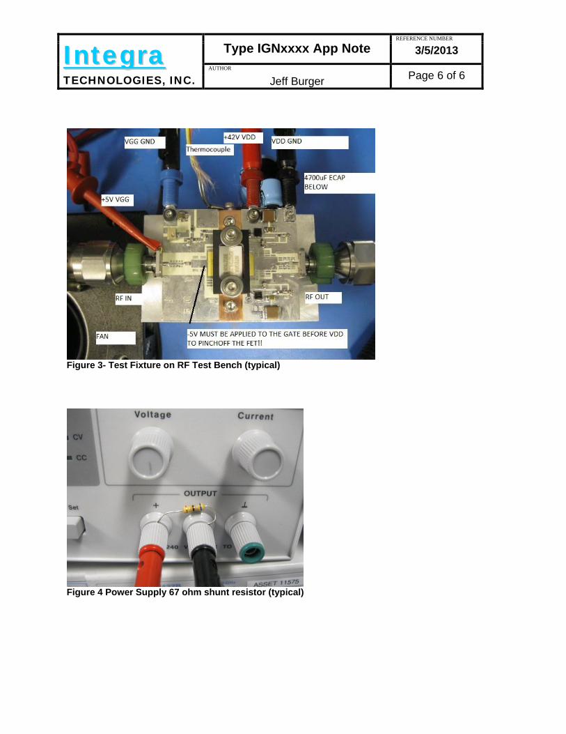
5. The gate side bias supply voltage should be adjustable to apply from at least -2 to -5V to the fixture gate. This is done by hooking up the positive gate supply voltage to the fixture ground, and the negative supply to the blue bias lead as shown. Set the current limit on the Gate supply to 100mA. Applying positive voltage to the Gate will damage the device. The Gate supply must be able to source and sink current into the Gate. At low RF power, the negative supply applied to the Gate (BLUE) will sink current. At high input RF power, the Gate supply will need to source current. Most bench power supplies cannot source and sink current. This problem can be solved by putting a shunt resistor across the terminals of the Gate supply (See Rshunt in Figure 4). The resistor value should be Rshunt < VGS, max/IGS,max. With VGS, max = 4.5 V, IGS, max = 10mA. Rshunt < 450 Ohms. Rshunt = 67 Ohms in Figure 4. The resistor power rating should be Pshunt > VGS, max^2 / Rshunt. In Figure 3, Pshunt > (5*5)/82 Ohms = 0.3W. Hookup the Gate supply as shown in Figure 4, with the positive supply terminal +5VGG on GND, and the negative supply terminal VGG GND on the Gate Bias (BLUE) jack. Adjust the VGG supply voltage to 5V. Verify that the voltage on the transistor Gate is -5V relative to the heat sink. Measure the resistance between VDD (RED) and ground (BLACK). You should measure greater than 10K Ohms through the device Drain if the Gate supply voltage is properly applied. This value may change slightly depending on the drain leakage current, but you should measure a high impedance from drain to source since the channel is turned off.
6. Next connect the Drain supply VDD as shown in Figure 3 with the supply turned OFF. Set the power supply current limit such that it, in conjunction with the charge storage capacitance, can handle the maximum peak current expected for the device. Make sure that the charge storage (4700uF) filter cap (Figure 2) is connected between the VDD (RED) and VDD GND (BLACK) terminals of the test fixture as shown in Figure 3. Next attach the power supply voltage sense leads to the VDD and VDD GND terminals, if available from the supply. Make sure that the power supply is in remote current sense mode. Otherwise, make sure to measure the Drain voltage at the terminals of the test fixture (RED to BLACK), and compensate for the voltage drop to the test fixture by adjusting the Drain supply voltage while testing the transistor. Hook up the main VDD supply lines to the VDD and VDD GND terminals. Size the supply wires appropriately.
7. Turn on the +VDD Drain power supply. There should be less than 10 mA of current drawn by the transistor Drain from the Drain supply, since the Gate bias is at -5V to keep the device in pinch off.
REFERENCE NUMBER Type IGNxxxx App Note 3/5/2013
AUTHOR IInntteeggrraa TECHNOLOGIES, INC. Jeff Burger Page 3 of 6
8. Adjust IDQ (drain quiescent current) using the VGS supply. Very slowly turn
the VGS supply voltage down in magnitude (10-50mV increments), to increase the Drain current to the desired IDQ. A fine resolution power supply adjustment knob is highly desirable to prevent overdriving the gate voltage, inducing excessive ID and potentially burning out the device. An Agilent E3610A power supply or equivalent is suitable. The Gate voltage should be around VGS = -2.7V to get the rated IDQ value.
9. Turn on the input RF power starting at low power (< 0.1W peak), and then increase until the desired output power is achieved. Correlation data is supplied with the clamped device. Please verify correlation before device removal per Section 6.
10. After testing is complete turn off the +VDD Drain supply voltage first. Leave the RF applied for about 5 seconds to discharge large charge storage Drain filter capacitor. Next, turn off the RF power. Lastly, turn off the Gate supply voltage.
11. The transistor should be handled in an ESD safe environment, with the operator properly grounded to prevent static discharge to the transistor, when removing and installing the transistor.
12. When inserting a new transistor, the device should be drain justified in the transistor slot. This means that the transistor should be pushed towards the drain side of the transistor slot before torqueing the clamp screws. The screws should be torqued sequentially to between 6-8 in/lbs. Before starting the turn on sequence of a new transistor please turn the Gate supply voltage back to 5V. Turn on the Gate supply, and measure the voltage on the Gate to GND. If you measure VGS = -5V, proceed to step 7 above.
13. IDQ SLOW TIME CONSTANT- If the RF is turned off from full power abruptly, the IDQ will require several minutes to recover to the original bias setting. This is due to trapping effects. Please do not readjust the IDQ as this will cause improper bias level adjustments. A better way to verify that the IDQ is still correct would be to reduce the RF input power with a variable attenuator until the RF is off. The IDQ in this case will be correct without waiting for time constant recovery.
REFERENCE NUMBER Type IGNxxxx App Note 3/5/2013
AUTHOR IInntteeggrraa TECHNOLOGIES, INC. Jeff Burger Page 4 of 6
3 Cooling The transistor will dissipate power and requires adequate cooling. At a minimum a biscuit fan model BT2A1 or equivalent should be provided. The fan can provide 22CFM of airflow over the fins of the heat sink. A #4-40 threaded screw hole is located on the copper transistor carrier to monitor the flange temperature. The typical TF (flange temperature) for RF testing is 30°C±5°C.
4 Thermal Grease Application (if required) Thermal grease was used for testing this part. Assuming that the transistor channel is clean, only a small dot of grease of 0.03-0.04” diameter is applied in the center of the slot. Do not use an excessive amount of grease. The grease pattern after transistor removal should not extend more than 0.25”. The correct amount of grease is required to obtain a thin coat that will not degrade electrical contact. Use Wakefield 120 or equivalent thermal grease. Make sure that the clamp is properly seated on the top of the flange, and that the screws are torqued sequentially to between 6-8 in/lbs.
5 Temperature Compensation The test fixture does not incorporate thermal compensation of the quiescent Drain current. The Gate bias voltage may need to be readjusted to maintain a constant IDQ, if testing with large variations in operating temperature.
6 Device Correlation The evaluation kit includes the test fixture, electrolytic cap, two transistors and RF test data. One of the devices is already clamped into the test fixture. The device has been tested at Integra as installed, and should be used for correlation purposes. Please compare data measured with Integra’s RF data for the serial number installed in the test fixture. Please also consult with the datasheet for additional information.
REFERENCE NUMBER Type IGNxxxx App Note 3/5/2013
AUTHOR IInntteeggrraa TECHNOLOGIES, INC. Jeff Burger Page 5 of 6
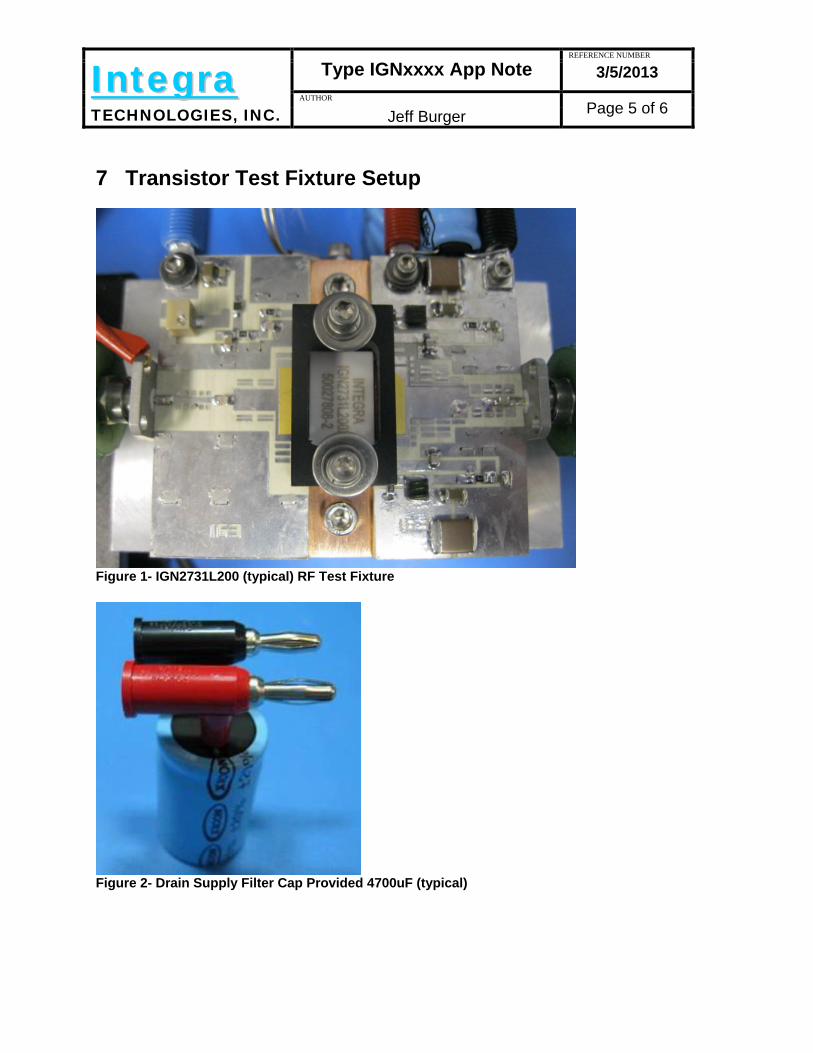
7 Transistor Test Fixture Setup
Figure 1- IGN2731L200 (typical) RF Test Fixture
Figure 2- Drain Supply Filter Cap Provided 4700uF (typical)
REFERENCE NUMBER Type IGNxxxx App Note 3/5/2013
AUTHOR IInntteeggrraa TECHNOLOGIES, INC. Jeff Burger Page 6 of 6
Figure 3- Test Fixture on RF Test Bench (typical)
Figure 4 Power Supply 67 ohm shunt resistor (typical)