High sensitivity MR sensors incorporated in silicon needles for magnetic neuronal response detection Marília Dias Silva Thesis to obtain the Master of Science Degree in Biomedical Engineering Supervisor: Prof. Susana Isabel Pinheiro Cardoso de Freitas Co-Supervisor: Prof. Ana Maria Ferreira de Sousa Sebastião Examination Committee: Chairperson: Prof. João Pedro Rodrigues Estrela Conde Supervisor: Prof. Susana Isabel Pinheiro Cardoso de Freitas Members of the Committee: Prof. Luís Humberto Viseu Melo December 2014
Transcript
High sensitivity MR sensors incorporated in silicon needles
for magnetic neuronal response detection
Marília Dias Silva
Thesis to obtain the Master of Science Degree in
Biomedical Engineering
Supervisor: Prof. Susana Isabel Pinheiro Cardoso de Freitas
Co-Supervisor: Prof. Ana Maria Ferreira de Sousa Sebastião
Examination Committee:
Chairperson: Prof. João Pedro Rodrigues Estrela Conde
Supervisor: Prof. Susana Isabel Pinheiro Cardoso de Freitas
Members of the Committee: Prof. Luís Humberto Viseu Melo
December 2014
ii
iii
Agradecimentos
Em primeiro lugar, gostaria de agradecer à minha orientadora, Prof. Susana Freitas pela
oportunidade de trabalhar no INESC-MN assim como pelo seu apoio e ajuda durante este projecto.
Agradeço ao José Amaral, por ter sido meu “co-orientador”. Todo o conhecimento que me
transmitiu, por todos os conselhos e explicações que me deu quando eu precisava e por toda a ajuda
no trabalho experimental e laboratorial. Sem esta ajuda tudo teria sido mais complicado.
Um obrigado a todos os colegas do INESC-MN que sempre se mostraram disponíveis para
me ajudar e tornaram o INESC um bom local de trabalho.
Agradeço também aos técnicos da sala limpa que me ajudaram nos processos de
microfabricação.
Finalmente agradecer a toda a minha família por todo o apoio que me tem dado. Em especial
aos meus pais, Paula e Mário, e ao meu irmão Rafael pela constante motivação, pela paciência, por
estarem presentes em todos os momentos. Um muito obrigado!
iv
v
Resumo
O trabalho efectuado nesta tese foca-se na medição de campos magnéticos originados no
cérebro. Compreender como o cérebro funciona é ainda um desafio para os neurocientistas por isso é
importante desenvolver uma ferramenta capaz de detectar campos magnéticos pequenos na ordem
do picoTesla gerados no cérebro.
Um equipamento de medida do potencial de campo local (LFP) localizado no Instituto de
Medicina Molecular (IMM) foi usado para desenvolver experiências com dispositivos planares ou
agulhas com sensores magnetoresisitivos (MR) funcionando como elemento de medida. Nas
experiências foram usadas fatias de cérebro de rato para medir o campo magnético criado pela
actividade neuronal.
Esta tese descreve todos os passos desenvolvidos para a fabrico e optimização de uma
ferramenta experimental em neurociências. Os sensores MR (válvulas de spin e junções de efeito de
túnel) são usados como ferramenta que permite medir sinais magnéticos pequenos em experiências
in vivo ou in vitro à temperatura ambiente. Foram fabricados diferentes sensores para conseguir
elevadas detectividades e um baixo nível de ruído. Os melhores sensores com maior sensibilidade e
uma componente do ruído 1/f reduzida são capazes de atingir detectividades abaixo de 1 nT a 30 Hz
e centenas de pT a 1 kHz.
Palavras-chave: Neurociência, Hipocampo, Actividade neuronal, Campo magnético,
Sensores Magnetoresistivos, Microfabricação.
vi
vii
Abstract
The work conducted in this thesis focused on the recording of magnetic signal from the brain.
Understanding how the brain works is still a challenge for neuroscientists so it is important to develop
tools capable to detect weak magnetic fields on the pT range generated in the brain.
A Local Field Potential (LFP) setup at Instituto Medicina Molecular (IMM) was used in order to
perform the experiments with a magnetoresitive (MR) planar array chip or a probe as measuring
element. In the experiments a rat brain slices were used to measure the magnetic field created by the
ionic currents.
This thesis describes all steps carried out towards the development and optimization of an
experimental tool in neurosciences. The magnetoresistive sensors (spin valve and magnetic tunnel
junction) are used as a tool which allows measuring weak magnetic signals at room temperatures in in
vitro and in vivo experiments. Different designs were made in order to achieve high detectivities and
low noise level. The best sensors with high sensitivities and reduced 1/f noise component were able to
reach detectivities down to 1 nT at 30 Hz and hundreds of pT at 1 kHz.
Keywords: Neuroscience, Hippocampus, Neuronal activity, Magnetic field, Magnetoresistive
sensors, Microfabrication.
viii
ix
Contents
Contents ................................................................................................................................................ ix
List of Figures ........................................................................................................................................ xi
List of Tables ........................................................................................................................................ xv
List of Abbreviations ............................................................................................................................ xvii
I. Introduction..................................................................................................................................... 1
1. Goals of the thesis ...................................................................................................................... 2
2. State of the art ............................................................................................................................ 3
II. Background theory ......................................................................................................................... 7
6.1. In vitro experiments .......................................................................................................... 49
6.2. In vivo experiments ........................................................................................................... 54
VI. Conclusions .............................................................................................................................. 55
Appendix I ............................................................................................................................................ 57
Appendix II ........................................................................................................................................... 67
Figure III-16: Magnetic tunnel unction structure sc ematic comprising layer composition and t ickness
in . ...................................................................................................................................................... 31
Figure III-17: MTJ bottom electrode definition: a) bottom electrode scheme b) single MTJ c) Array of
Figure III-20: MTJ top electrode definition scheme. ............................................................................. 33
Figure III-21: MTJ final passivation scheme. ........................................................................................ 33
Figure III-22: Wirebonding: a) 3 MTJ sensors which contacts are connected to flexible cable and
protected with silicone gel b) Planar MR sensor wire bonded to a flex cable and protected with
silicone gel ............................................................................................................................................ 34
Figure III-23 : Schematic representationof 4 contacts measurement in a) MTJ b) SV. ......................... 34
Figure III-24: Noise setup: a) spectrum analyser and main box b) main box: amplifier (SRS), testing
box and power supply c) testing box. ................................................................................................... 35
Figure III-25: Circuit of the noise measurement setup showing the different components. .................. 35
Figure III-26: Manual measurement setup composed of current source, voltmeter, Helmholtz coils and
micropositioners and a magnetotransport curve obtained for one of the fabricated MTJ sensors. ....... 36
Figure III-28: Signal acquisition setup MR chip connected to PCB which is connected to ADC that
sends the data to Matlab software. ....................................................................................................... 38
Figure III-29: Circuit of the signal acquisition setup showing the different components. ...................... 38
Figure III-30: Electronic setup: a) recording chamber and electronics b) PCB with a needle, CMOS
circuit and flex cable. ............................................................................................................................ 39
Figure III-31: LFP system and recording chamber at IMM. .................................................................. 39
Figure III-32: Stimulus and recording electrode position in the on hippocampus slice. ........................ 40
Figure IV-1: Autocad mask design and device with 15 sensors with one MTJ. .................................... 41
Figure IV-2: Transfer curves of sensors in one die and transfer curve of MTJ sensor with best MR. ... 42
Figure IV-3: Noise values of one MTJ sensor for different bias voltage and respectively detectivities. 42
Figure IV-4: Chip design with 15 arrays of MTJ sensors, 8 arrays with 84 sensors in series and 7
arrays with 140 sensors in series. ........................................................................................................ 43
Figure IV-5: Transfer curves of all sensors in the planar device and transfer curve of the sensor 6 with
140 MTJ sensors in series. ................................................................................................................... 43
Figure IV-6: Voltage noise density (nV/√Hz) obtained from t e noise measurement setup and
detectivity (nT/√Hz) calculated from t e values of noise and sensitivity. .............................................. 43
Figure IV-7: Autocad mask for large device (7100x6500µm2) and small device (3550x3250µm
2). ...... 44
Figure IV-8: Final devices: large and small device. .............................................................................. 44
Figure IV-9: Transfer curve of all sensors with 952 MTJ in series and transfer curve of sensor with
small area and the highest value of MR. .............................................................................................. 45
Figure IV-10: Noise values for 952 MTJ in series and detectivities for bias voltage of 4.76 V, 1.11 V
and 476 mV. ......................................................................................................................................... 45
Figure IV-11: Autocad mask for small and large area arrays of SV and scheme of parallel of series SV.
Figure IV-12: Transfer curves of 6 sensors with 6200 SV in series and transfer curve of the sensor
with the best MR. .................................................................................................................................. 47
xiii
Figure IV-13: Noise measurement of 6200 SV in series and detectivity. .............................................. 47
Figure IV-14: SV needles: a) 175 µm width with two individual sensors b) 1mm width with two arrays of
992 elements c) 320 µm with two individual SV with flux guides. ......................................................... 48
Figure IV-15: Transfer curve of a single SV and the array of 992 SV. .................................................. 48
Figure IV-16: Transfer curve of a single SV with a flux guide. .............................................................. 49
Figure IV-17: Hippocampus brain slice on top of the sensor the green zones are plasticine used to
immobilize the cable during the experiment. ........................................................................................ 50
Figure IV-18: Noise measurement of the sensor with air, water and krebs solution at IMM. ................ 50
Figure IV-19: Electrical signal recorded by recording electrode. .......................................................... 51
Figure IV-20: Output signal measured in a rat hippocampal slice with a single MTJ sensor. ............... 52
Figure IV-21: Output signal measured in a stimulated rat hippocampal slice with a single MTJ sensor
with averages a) after 10 minutes b) after 15 minutes. ......................................................................... 52
Figure IV-22: Corrosion and damage in the sensors after experiments. .............................................. 53
Figure IV-23: Experiment with hippocampus slice and a SV needle. ................................................... 53
Figure IV-24: Device for in vivo experiments. ....................................................................................... 54
xiv
xv
List of Tables
Table III-1: Etching conditions in N3600. .............................................................................................. 24
Table III-2: Conditions for different modules present in N7000. ........................................................... 25
Table III-3: UHV I deposition conditions for CoZrNb. ........................................................................... 25
Table III-4: Deposition conditions for the Al2O3 target on UHV II. ......................................................... 26
Table III-5: List of SV stacks used in microfabrication process. ........................................................... 27
Table III-6: MTJ stack used in microfabrication process. ..................................................................... 31
Table IV-1: Summary of the fabricated MR sensors. ............................................................................ 46
Table IV-2: Summary of SV arrays characterization. ........................................................................... 46
The recording of brain signals provides valuable information for physiologists and neuroscientists
to understand the brain. Measurements associated with the neural currents in the brain can be used to
diagnose epilepsy, stroke, mental illness and how the brain works [1].
One way to observe the electrical currents is to measure the magnetic fields they produce outside
the skull, through a technique called magnetoencephalography (MEG). However, MEG has been
demonstrated to be a useful, noninvasive clinical tool for the localization of synchronized (e.g.
epileptic) neuronal activity within the human brain, particularly when combined with simultaneous
electrical measurements. These types of measurements reflect only the activity of a macroscopic
neuron population. The traditional way to monitor the brain’s electrical activity is with
electroencephalography (EEG).
The strongest electrophysiological signals are generated by heart and by skeletal muscles. The
amplitude corresponding to contraction of the cardiac muscle is several tens of picotesla. From the
normal awake brain, the largest field intensity is due to spontaneous activity. T e α-rhythm observed
over the posterior parts of the head is 1-2 pT in amplitude. Abnormal conditions, such as epileptic
disorders, may elicit spontaneous spikes of even larger amplitudes. Evoked fields following sensory
stimulations are weaker than pT by an order of magnitude or more [2].
Since the magnetic field decreases with the square of the distance, the signal can be measured
directly from the neuron to obtain the information with a minimum signal loss
To measure such small signals, the sensors should have the high sensitivity, low intrinsic noise
and enhanced resistance to corrosion in the presence of biological tissue and media. These
parameters will be studied during this work.
This thesis target is the measurement of magnetic field generated by ionic currents from rat
hippocampal slice with MR sensors.
First, a state of the art is given followed by the framing of this work within the ongoing studies in
the group, finishing by the specific goals set for this thesis.
The origins and mechanisms of neuronal signal propagation are introduced, followed by the
fundaments of magnetoresistance and noise crucial for the used sensors and given their importance
for intensity of signals being measured.
The third chapter describes the deposition systems and microfabrication techniques and depicts
two different microfabrication processes step by step. On a second part, the equipment and setups
used to characterize the devices will be described.
In the fourth chapter, the transfer curves and noise characterization of the sensors and the results
of the experiments on hippocampal brain slice from rat performed at IMM will be explained and
discussed.
The fifth chapter is a conclusion of this thesis and shows the future perspectives of this work.
A run-sheet will be provided in Appendix I, as well as examples of the masks used along the process.
A list with steps of microfabrication SV sensors with flux guides will be given in Appendix II.
2
1. Goals of the thesis
T e magnetic field intensity generated by living tissues range from ≈ 1 fT (nerves) to tens of pT
(human heart) [3], thus the signal is not strong enough to be measured by the magnetic sensors
located outside the skin.
Nowadays the technique used to record the brain magnetic fields on the scalp is the MEG.
However, the recorded information arises from a population of neurons. Thus to understand all
processes that occur in the brain a study in the individual signals is necessary.
Since magnetic fields are weak, the task of measuring them is challenging in terms of required
sensor sensitivity and also the ability to suppress interference of several orders of magnitude stronger
than the signals of interest.
In this work, the first challenge is to develop sensors with a high sensitivity (nT to pT) and low
noise. In order to achieve this, the design and fabrication of different devices with magnetoresistive
sensors, spin valve and magnetic tunnel junction, will be performed. The devices will be planar and
probes with single sensors and arrays. The flux guides will be also introduced to allow the
concentration of magnetic flux at the sensor.
The other challenge is measure magnetic field in a rat hippocampal slice. These studies are
advantageous since the brain slices can sustain certain electrophysiological characteristics typical of
the intact brain consequently opening a wide range of possibilities for studying cerebral tissue in vitro.
The rat hippocampal slice preparation is the most studied. Many studies demonstrate that neurons in
brain slices are in a healthy state because they maintain their synaptic potential and exhibit synaptic
plasticity. The hippocampus is a part of the brain and has pyramidal cells. Pyramidal cells are a
population of neurons spatially organized which neurons are parallel to each other creating a Local
Field Potential (LFP). These potentials create a magnetic field that can be recorded by the sensor.
The magnetic field at 10 μm distance for a single neuron is ~ pT to few nT.
MR planar devices and probes are designed with size and materials compatible with the biological
tissue and the solution used in vitro experiments and also fabricated to be compatible with the system
at IMM (Instituto Medicina Molecular) where the experiments in vitro are done. The experiments are
performed in a LFP electrophysiology system where the slice is in contact with the sensors.
The electronic acquisition setup that provides MR sensors biasing, signal amplification and filtering
and the software (Matlab) allows signal visualization, storing and digital filtering for the measured
signal are developed by INESC-ID. The system is adapted to the LFP system at IMM and to the
conditions of the experiments. Due to the weakness of the signal some methods (averaging and
filtering) are developed in order to reduce the noise levels increasing the possibility to measure the
magnetic field.
3
2. State of the art
Brain waves carry important and highly pertinent information relatively to the control of the human
body. The challenge of neuroscientists has been to record the brain waves from neurons directly or
from the whole brain, that is, from the scalp.
At the microsopic level, the signals are produced by neurons, specifically the action potentials
(also commonly termed as 'spikes'). Microelectrodes inserted into the brain and in the vicinity of
neurons serve to record the spikes. At a macroscopic level there are different options: to record the
electrocorticographic (ECoG) signal or the Electroencephalogram (EEG). The ECoG signal is
recorded by placing an array of electrodes directly onto the brain surface (requiring brain surgery),
while the EEG signals are recorded by placing an array of electrodes on the scalp. This technique is
noninvasive but signals are small and can be noisy. Functional magnetic resonance imaging (fMRI) or
magnetoencephalogram (MEG) are used for functional neuroimaging.
Electroencephalography (EEG) is the measurement of the brain’s electrical activity obtained from
recording electrodes placed on the scalp [4]. The currents are generated by synchronized synaptic
currents arising on cortical neurons. High frequencies such as those produced by action potentials, are
subject to a severe attenuation, and therefore are only visible for electrodes immediately adjacent to
the recorded cell. On the other hand, low-frequency events, such as synaptic attenuate less with
distance. The resulting traces represent an electrical signal from a large number of neurons. The EEG
is capable of detecting changes in electrical activity in the brain on a millisecond-level. It is one of the
few techniques available that has such high temporal resolution [5].
Magnetoencephalography (MEG) is a non-invasive functional brain imaging technology. This
extremely sensitive technology measures the magnetic fields produced by electrical neuronal activity
at numerous different positions around the head. Electrical currents in the cortex produce a magnetic
field around fentoTesla.
In 1967, David Cohen built a magnetic shielded room to record weak magnetic signals emmited
from the heart. Shortly after, he pioneered in measuring the magnetic field of the brain in a multilayer
magnetically shielded chamber and introduced the MEG [6]. Later on, James Zimmerman invented a
highly sensitive magnetometer, called Superconducting Quantum Interference Device (SQUID) which
is based on superconducting loops containing Josephson junctions. By adapting SQUIDs,
magnetoencephalography became much more sensitive to weak magnetic fields. David Cohen
measured the alpha rhythm in a healthy human and also recorded the abnormal activity of an epileptic
patient [7]. SQUID-sensor units operate at low temperature and are typically housed in a thermos like
container filled with liquid helium. Moreover, some efforts have been made to measure the magnetic
field at higher temperatures such as a magnetic field sensor that combines a superconducting flux-to-
field transformer with a low-noise giant magnetoresistive sensor. This type of sensor can reliably
operate at temperatures up to 77K and a prototype of this design has shown the ability to successfully
measure 32 fT/√Hz [8]. Biomagnetic recordings (magnetic signatures of the electric activity of the
human heart) at 4 K with hybrid sensors based on Giant MagnetoResistance (GMR) were reported
and detectivities around 3pT/√Hz were ac ieved [9].
4
In addition functional magnetic resonance imaging (fMRI) works by detecting the changes in blood
oxygenation and flow that occur in response to neural activity (when a brain area is more active it
consumes more oxygen and, as such, to meet this increased demand the blood flow increases
towards the active area). fMRI can be used to produce activation maps showing which parts of the
brain are involved in a particular mental process. The increased use of the technique is due to its
availability, high spatial resolution, relatively high temporal resolution, and lack of ionizing radiation or
need for external contrast agents[10].
A variety of in vitro preparations have been used in experimental neuroscience research. They
range from isolated single neurons to cell cultures, brain slices, and sometimes whole brain
preparations. All these techniques have high resolution. Brain slice preparations are becoming
increasingly popular among neurobiologists for the study of the mammalian central nervous system
(CNS) in general and synaptic phenomena in particular.
There are two types of measurements that can be electrical and magnetic.
Any excitable membrane (dendrite, soma, axon or axon terminal) and any type of transmembrane
current contribute to the extracellular field. The field is the summation of all ionic processes, from fast
action potentials to the slowest fluctuations in glia. Electric current contributions from all active cellular
processes within a volume of brain tissue generate a potential with respect to a reference. The
difference in potential between two locations gives rise to an electric field. Electric fields can be
monitored by electrodes placed extracellular with millisecond time resolution and can be used to
interpret many issues of neuronal. A major advantage of extracellular field recording techniques is
that, in contrast to several other methods used for the investigation of network activity, the biophysics
related to these measurements are well understood [11].
These electrical currents produced a magnetic field which can be measured. The magnetic
measurements have advantages in relation to the electric measurements. Since magnetic field is a
vector quantity providing more information than a scalar value (single potential), does not require
contact with neurons and does not need a reference point to perform the measurements.
Early studies using in vitro preparations allowed the measurement of magnetic field generated by
neuronal activity. A calculation of the magnetic field around an axon was performed by Swinney and
Wikswo (1980) using a preparation whereby an isolated axon from frog sciatic nerves was kept in a
bath saline, in vitro, and was stimulated electrically. They found that the resulting magnetic field is ~
60 pT at 1.3 mm [12].
Yoshio Okada and colleagues applied some models to a section of a guinea pig hippocampal slice
kept in an in vitro bath, while measuring simultaneously the intracellular electric potentials of CA3
pyramidal cells, the extracellular field potentials and the magnetic fields, four detection coils connected
to µ-SQUIDs. They measured magnetic fields around 10 pT where the distance between the slice and
the detectors was 2000 µm [13].
Tesche and colleagues made measurements in slice of hippocampal tissue from male guinea pig.
The magnetic measurements were obtained by a low noise DC SQUID and the slice was located
approximately 17000 µm below the bottom set of coils. A magnetic field of 300-400 fT was observed
[14].
5
A high-transition-temperature superconducting quantum interference device (HTC SQUID) system
was used in magnetic measurements of evoked fields from in vitro hippocampal slices from rat. The
evoked neuronal activity produced magnetic fields of ~5 pT [15].
The ability of magnetoresistive sensors to detect very weak magnetic fields (nT) at room
temperature is being used in a growing number of new applications other than magnetic recording. At
INESC-MN, research on systems capable to measure action potentials at room temperature is
currently ongoing. Silicon probes with giant magnetoresistance (GMR) and tunneling
magnetoresistance (TMR) technologies integrated have achieved detectivities down to 30 nT/√Hz at
room temperature [16][17]. These silicon probes have been explored in the European project
MAGNETRODES (Electromagnetic detection of neural activity at cellular resolution). The goal of this
project is to develop a tool for magnetic imaging at neuron scale in order to model the electromagnetic
response of a neuron. Detectivities of 90 pT/√Hz ave already been reported [18] and for large areas
and low aspect ratio devices detectivities of 46 pT/√Hz were reac ed [19].
6
7
II. Background theory
1. Brain
In the 18th century Galvani demonstrated that most of the physiological processes were
accompanied with electrical changes. The muscles and the heart are two well-known and strong
sources of electrophysiological currents. The brain also sustains ionic current flows within and across
cell assemblies, with neurons acting as the strongest generators [20].
1.1. The nervous system
The nervous system consists of the brain, spinal cord and peripheral nerves and is composed of
nerve cells called neurons. The brain consists of the brain stem and the cerebral hemispheres [21].
There are three types of neurons: sensory neurons, motor neurons and interneurons. The sensory
neurons are specialized to detect and respond to different aspects of the internal and external
situations. Motor neurons are responsible for the control of the activity of muscles whereas
interneurons mediate simple reflexes and are responsible for the highest functions of the brain.
Neuron’s architecture consists of a cell body, axons and dendrites (Figure II-1). The cell body forms
the central part of the neuron and contains the nucleus of the cell. Axons transmit information from
one neuron on to other to which it is connected and dendrites receive the information being
transmitted by the axons of other neurons. The two principal groups of cortical neurons are the
pyramidal and the stellate cells. Pyramidal cells are the most populous cell type. They have long,
parallel to each other, thick apical dendrites that can generate strong dipoles along the
somatodendritic axis. Such dipoles give rise to an open field, as there is considerable spatial
separation of the source from the return currents. This induces substantial ionic flow in the
extracellular medium.
Two distinct types of axons occur in the peripheral and central nervous system (PNS and CNS):
unmyelinated and myelinated axons. Myelinated axons can be considered as three compartments: an
initial segment where somatic inputs summate and initiate an action potential; a myelinated axon of
variable length, which must reliably transmit the information as trains of action potentials; and a final
segment, the preterminal axon, beyond which the synaptic terminal expands [22][23]. The small gaps
between sucessive segments of the myelin sheath are called nodes of Ranvier. The nerve impulse in
a myelinated fiber jumps from node to node, thus speeding passage and reducing energy
requirements.
8
Figure II-1: Neuronal cell structure: dendrites, cell body and axon [23].
The brain and spinal cord are connected to both sensory receptors and muscles through long
axons that make up the peripheral nerves.
The cell membrane of neurons is a very thin (7 to 15 nm) lipoprotein complex that is essentially
impermeable to intracellular protein and other organic anions (A-). In the resting state the membrane is
only slightly permeable to Na+ and rather freely permeable to potassium (K
+) and chloride (Cl
-). The
permeability of the resting membrane to the potassium ion (PK) is approximately 50 to 100 times larger
than its permeability to sodium (PNa). When the ion channels are closed, the concentrations of K+ and
Cl- ions inside the cell are high in relation to the cell’s outside, w ereas the concentration of sodium
(Na+) is high outside the cell in relation to the cell’s inside. The difference in concentration creates a
diffusion gradient that is directed outwards across the membrane. Due to this ions movement a
transmembrane potential is created, the interior of the cell is more negative than the external medium.
The electric field of the membrane at rest is directed from the outside to the inside and from
positive to negative across the membrane. With this the positively charged ions do not flow to the
outside and the negatively charged ions remain inside the membrane. Thus the diffusional and
electrical forces acting across the membrane are opposite and a balance is ultimately achieved.
The membrane potential when equilibrium occurs is called equilibrium potential. This equilibrium
is calculated from the Nernst equation at 37°C (body temperature):
II.1
Here n is the valence of the K+, [K]i and [K]o are the intracellular and extracellular concentrations of K
+
in moles per liter, respectively, R is the universal gas constant, T is absolute temperature in K, and F
is the Faraday constant. Equation II.1 provides a reasonably good approximation to the potential of the
resting membrane, which indicates that the resting membrane is effectively a potassium membrane.
Goldman (1943) and later Hodgkin and Katz (1949) developed an equation for the membrane
equilibrium potential (E) which accounts for the influence of other species in the internal and external
media called the Goldman-Hodgkin-Katz Formulation:
.log0615.0ln 10
i
O
i
O
KK
K
K
K
nF
RTE
9
,ln 00
oCliNaiK
iClNaK
ClPNaPKP
ClPNaPKP
F
RTE
II.2
where E is the equilibrium transmembrane (resting) potential when the net current through the
membrane is zero and PM is the permeability coefficient of the membrane for a particular ionic species
M.
Maintaining the steady state ionic imbalance between the internal and external media of the cell is
necessary through continuous active transport of ionic species against their electrochemical gradients.
This transport mechanism is done throughout the membrane and is called the sodium potassium
pump. It actively transports Na+ out of the cell and K
+ into the cell. Furthermore, this mechanism needs
energy produced by mitochondria - adenosine triphosphate (ATP).
At rest, the cell membrane potential defined with respect to the inside of the cell is about -70 mV,
due to the steady resting potential the cell membrane is said to be polarized. An excitable cell has
another property, which is the ability to conduct an action potential when adequately stimulated. This
stimulus should bring about the depolarization of a cell membrane that is sufficient to exceed its
threshold potential and in that way cause an all-or-none action potential, which travels at a constant
conduction velocity along the membrane. The origin of the action potential lies in the voltage and time
dependent nature of membrane permeabilities to specific ions, notably Na+ and K
+. As the
transmembrane potential is depolarized, the membrane permeability to sodium PNa is increased.
Consequently, Na+ rushes into to the cell along the concentration gradient. This influx of Na
+ causes
the membrane to become even more depolarize, thus, causing the activation of more Na+. This influx
of Na+, into the cell, results on the rising phase of the action potential. Once the cell reaches a peak
depolarization the Na+ channels close and the K
+ channels open. Now, K
+ ions flow out of the cell
along the concentration gradient, and the cell membrane begins to hyperpolarize. This efflux of K+
results in the falling phase of the action potential and hyperpolarization continues until the cell has
returned to its resting potential (Figure II-2 a)).
Figure II-2: a) Action potential b) Magnetic field generated by a neuron’s action potential. Taken from [24].
When an excitable membrane produces an action potential the ability of the membrane to respond to
a second stimulus of any sort is markedly altered. During the initial portion of the action potential, the
a) b)
10
membrane cannot respond to any stimulus, no matter how intense. This interval is referred to as the
absolute refractory period. It is followed by the relative refractory period, wherein an action potential
can be elicited by an intense superthreshold stimulus. The existence of the refractory period produces
an upper limit to the frequency at which an excitable cell may be repetitively discharged [25][26].
Actions potentials are transmitted along axons to regions called synapses, where the axons
contact the dendrites of other neurons. These consist of a presynaptic nerve ending separated by a
small gap from the postsynaptic component, which is often located on a dendritic spine. Synapses
provide an unidirectional flow of information, from the sending (presynaptic) to the receiving
(postsynaptic) neuron, but not in a reverse direction. At most synapses the cause of change in
potential of the postsynaptic membrane is chemical. The transmission across this gap is done by
chemical messengers called neurotransmitters [23].
The post synaptic potentials (PSP) looks like a current dipole oriented along the dendrite. The
strength of the current source decreases with the distance of the synapse, however about a million
synapses must be simultaneously active during a typical evoked response. The strength is around
20 fAm for a single PSP. Since there are approximately 103 pyramidal cells per mm
2 of cortex and
thousands of synapses per neuron, the simultaneous activation of a few synapses in a thousand over
an area of one square milimeter would suffice to produce a detectable signal. pAm corresponds to
currents of few to several tens of nA. At approximately 10 μm, a 100 nA current creates a magnetic
field in the order of nT. The PSP are the main source of MEG.
The action potential can be approximated by two oppositely oriented dipoles and the magnitude
of each dipole is about 100 fAm. A dipolar field, produced by synaptic current flow, decrease with the
distance as 1/r2 [2].
A propagating action potential produces a magnetic field, which is calculated from the
transmembrane action potential (Figure II-2 b)).
1.2. Hippocampus
The hippocampal region is the part of the cerebral cortex. The ventromedial area of the human
temporal lobe contains the amygdala, the hippocampal region, and superficial cortical areas that cover
the hippocampal region thus forming parahippocampal gyrus. The hippocampal region can be
subdivided into three subregions: the dentate gyrus, the cornu Ammonis (CA) sectors, and the
subiculum [27]. The hippocampal formation play a central role in memory function in humans [28].
The Figure II-3 shows the pathway of hippocampus signal transmission. The main input to the
hippocampus (perforant pathway (pp)) arises from the entorhinal cortex and passes through to the
dentate gyrus. From the granule cells of dentate gyrus connections are made to area CA3 of the
hippocampus proper via mossy fibers (mf). CA3 sends connections to CA1 pyramidal cells via the
Schaeffer collateral (Sch) as well as commissural fibers (comm) from the contralateral
hippocampus. The major neurotransmitter in these three pathways is glutamate. The final output
from the two CA fields passes through the subiculum entering the alveus, fimbria, and fornix and then
to other areas of the brain [29].
11
In the rat hippocampus, the most characteristic collective patterns are oscillations in the theta (6–
10 Hz), gamma (40–100 Hz) and ultra-fast (140–200 Hz) bands. Theta waves depend on ongoing
behavior and are most consistently present during rapid eye movement (REM) sleep [30].
Figure II-3:Pathway of hippocampus signal transmission [31].
1.3. Local field potential
Different cellular mechanisms are responsible for different frequency components of the recorded
signals.
Coherent membrane currents brought about by synaptic activity and intrinsic properties of
neurons, pass through the extracellular space and can be measured by electrodes placed outside the
neurons as local field potentials (LFP).
The high-frequency content about 600–6K Hz is referred to as unit activity, while the low-
frequency signal content below about 600 Hz is referred to as local field potential.
LFPs come from several sources; the most significant of these is the synaptic activity. Because the
capacitive lipid membranes of cells in the brain act as a low pass filter, the high-frequency
components of neuronal signals are greatly attenuated as they travel through the extracellular
medium. Equivalently, slow signals are able to propagate much farther than are high frequency
signals. As a result, the low-frequency component of the signal recorded at any given point within the
brain is a linear sum of the activity from large populations of cells. Thus, LFP can be interpreted as an
indication of the cooperative actions of neurons[32][33][34][35].
One of the simplest and widely used model of LFP activity considers currents’ sources embedded
in a homogenous extracellular media, however this model does not account for the frequency-
dependent attenuation and therefore is inadequate for modeling extracellular fields potentials. A new
model was described taking into account the nonhomogeneous media [5] and the calculations of the
extracellular LFP were made through the usage of this model. This was used to calculate the field
potentials at different radial distances assuming the neuron was a spherical source. The extracellular
potential is indicated for 5, 100, 500 and 1000 µm away from the source. The Figure II-4 shows the
results of the calculation.
12
Figure II-4: Membrane potential of a single compartment model, total membrane current and extracellular potential calculated at various distance from source [5].
The electric properties of media can influence the electric field and also the magnetic field. The
generalized cable formalism is an important tool to calculate the extracellular electric and magnetic
fields generated by neurons. The nature of the medium influence both types of fields [36]. However,
the electric signal suffers distortion and attenuation due to properties of the soft and hard tissues
between the current source and the recording electrode. Magnetic signals are much less dependent
on the conductivity of the extracellular space but they are dependent of the distance from the source
current. The magnetic field decays 1/d2. An estimation of the magnetic field at 10 μm distance for a
single neuron which has current amplitude of 10 to 100 nA, yields a magnetic field of about pT to few
nT.
2. Magnetoresistance
Magnetoresistance (MR) is a phenomenon that reflects the resistance change of a material when
an external magnetic field is applied to it. The major application of MR sensors is for read heads in
hard disk drives for the data storage market.
The MR effect can be categorized into five distinct types including ordinary magnetoresistance
magnetoresistance (TMR) and colossal magnetoresistance (CMR).
This effect is measured by applying a variable magnetic field which cause the variation of the
electrical resistance between a minimum value (Rmin) and a maximum one (Rmax) and it is expressed
as a ratio found in equation II.3:
II.3 100
min
minmax
R
RRMR
13
2.1. Giant magnetoresistance (GMR)
Giant magnetoresistance was first observed in a multi-layered thin-film structural material
composed of two ferromagnetic (FM) Fe layers separated by a non-magnetic Cr layer in 1988 by Fert
(at low temperatures) [37] and by Grunberg at room temperature [38].
One of the applications of GMR is the Spin Valve (SV) first proposed in 1991 by Dieny [39].
Spin valve consists of two FM layers (alloys of Fe, Co and Ni) separated by a non-magnetic metal
spacer layer (Cu, Ag and Au). One of the two FM layers is called the pinned layer, in which the
magnetization is relatively insensitive to the moderate magnetic field. The other FM layer is called the
free layer, in which applying a relatively small magnetic field could change the magnetization. The
pinned magnetic layer is often connected to an antiferromagnetic layer (FeMn, NiO, MnIr, MnRh) or an
antiferromagnetically coupled multilayer (Co/ Ru (or Re)/ Co). The relative orientation of the free layer
with respect to the pinned layer will give different resistance states and when controlled can originate
a square response, which can be used as a memory, or a linear response, used as a sensor. o e
and Ni e are usual c oices for t e ferromagnets and t eir t ickness is 1 -30 , t e spacer t ickness
is 2 and t e material is u and Mn r is t e metal c osen as antiferromagnetic.
The GMR effect arises from the asymmetry in the spin-dependent scattering at the non-
magnetic/magnetic interfaces for spin-up and spin-down electrons. When the magnetic layers are
aligned in parallel, the current is mostly carried by spin-up electrons, which can easily pass through
the entire material while experiencing a weak scattering process and leading to a lower resistance
state. However, when the magnetic layers are anti-parallel, both spin-up and spin-down electrons
scatter strong at different parts of the materials and the scattering probability is equal for both classes
of electrons, leading to an overall higher resistance [40][41].
The values of MR for standard spin valves can reach up to 9% at room temperature and can reach
20% with the introduction of additional nano-oxide-layers next to the ferromagnets [42].
Since their discovery, GMR materials have been widely used in many areas including rotation
speed sensing in automotive systems, angular position sensing, magnetic recording and writing heads
(hard disc drivers), magnetocardiography sensors, drug delivery, biosensors and biochips for
biological detection, magnetic field sensors and MRAM.
Figure II-5: Structure of a spin valve: CoFe and NiFe are choices for the ferromagnets (FM), Cu is usually chosen as the metal (spacer) and MnIr for the antiferromagnetic layer (AFM).
14
2.2. Tunneling magnetoresistance (TMR)
In 1975, Julliere was the first who reported the tunneling magnetoresistance effect between two
ferromagnetic films [43].
The tunneling magnetoresistance (TMR) takes place in a magnetic tunnel junction (MTJ), which is
composed of two ferromagnets separated by a thin insulating tunnel barrier. The resistance depends
on the relative magnetization of the two magnetic layers and is different for the parallel and antiparallel
magnetic configurations of these two electrodes. T e electrode t ickness is 30- 0 and t e material
can be NiFe, CoFe and CoFeB alloys, MgO is the choice for the barrier and MnIr for the
antiferromagnet. The current flows perpendicular to the film plane.
The electrons travel from one ferromagnetic layer to another layer by the tunnel effect, a process in
which the spin has been conserved. Each electron that leaves a ferromagnetic layer will occupy the
state corresponding to its spin in the other ferromagnetic layer, meaning that the tunnelling of spin-up
and spin-down electrons are two independent processes. If both ferromagnetic layers have parallel
magnetizations, the majority states tunnel to fill the majority states and minority spins tunnel to fill
minority states. However, if both ferromagnetic layers have antiparallel magnetizations, the majority of
spins is tunneling to fill minority states while the minority of spins is tunneling to fill the majority states.
The TMR is defined as the current density difference between parallel and antiparallel and it is
given by:
II.4
where RP and RAP are the resistances with magnetizations of the electrodes parallel and antiparallel,
respectively.
A TMR value of around 14% was obtained at low voltage and 4.2 K [43]. Later, a room
temperature TMR value of 18% was obtained in the Fe/ Al2O3/ Fe junction system [44] and of 11.8%
was obtained in the CoFe/ Al2O3/ Co thin film tunnel junction system [45]. These values are a great
progress in the development of the room temperature TMR effect. The TMR effect is also observed in
the MgO barrier in the Fe/ MgO/ Fe is up to 180% [46] and in the CoFeB/ MgO/ CoFeB is 604% at
300K [47]. The tunneling resistance depends exponentially on the tunnel barrier thickness and is
characterized by the resistance-area (RA) product [45][48].
2.3. Sensor linearization
In this thesis the objective is to use the SVs and MTJs as sensors for magnetic field detection. As
such, the ideal GMR and TMR response should be linear with no hysteresis and symmetric (centered
at H=0 T). To achieve this response it is necessary that the rotation of the free layer magnetization
between the parallel and anti-parallel states with respect to the pinned layer magnetization is
,)(
AP
PAP
R
RRTMR
15
coherent. This means that, the free and pinned layer magnetization have orthogonal directions when
there is no external field applied.
There are two main processes for inducing a linear response. The first is to deposit the MR films
applying orthogonal magnetic fields defining the crossed magnetic anisotropy and the second is to
control the shape of the sensor (the created demagnetizing field sets the free layer magnetization
perperdicular to the pinned layer).
MR films with crossed magnetic anisotropies refer to the orientation of the pinned and free layers
magnetization. The pinned layer anisotropy is fixed by exchange coupling with the antiferromagnetic
layer while the magnetic anisotropy of the free layer is defined in the perpendicular direction with
respect to the pinned one.
Figure II-6: Schematic of the crossed anisotropy in MR sensor. In crosses anisotropies, the free layer magnetization is set perpendicular to the pinned one, leading to a coherent rotation of the free layer.
Anisotropy directions can be set during deposition, by applying a magnetic field in the desired
direction. When an external field is applied along the pinned layer direction, the free layer rotates
coherently leading to a linear response of the MR sensor in the small field interval.
On the other hand, the dimensions of the MR sensor cause shape anisotropy in such a way that
the created demagnetizing field changes the free layer's magnetization leading to orthogonality
between the magnetization directions of the pinned and free layers.
For magnetic field sensing applications, the magnetization of the free layer is set perpendicular to
the pinned layer. To obtain such configuration other approach is used in this work for the MTJ. The
strategy is the deposition of a multilayer stack including two antiferromagnetic (AFM) thin films.
The latter consists in a multilayer stack with two AFM films: one near the pinned layer and the other
adjacent to the free layer. Both AFM layers set the magnetization of the ferromagnetic (FM) layers in a
fixed direction due to exchange interactions. The free layer is weakly pinned by an antiferromagnet
which has a lower exchange field in relation to the pinned layer one. To accomplish such configuration
the two exchange coupled interfaces (free and pinned layers) require different temperature stabilities.
Through two successive annealing steps at different temperatures with crossed applied fields the
required configuration is obtained. The first annealing at high temperature initializes both AFM pinned
layers in the same direction and a second annealing step at a lower temperature sets the weakly
pinned free layer at a magnetization perpendicular to the pinned layer.
16
3. Noise influence
Noise can be originated from different sources such as defect motion, magnetic domain or spin
fluctuations, charge carriers crossing an energy barrier, electronic traps and current redistribution
within inhomogeneous materials. Since they are presented they acts like fluctuators, i.e. they coupled
to the charge carriers constituting the current and induce specific resistance or current fluctuations
giving rise to noise [49]. Noise corresponds to random fluctuations in the current flowing through a
material or in the voltage measured across the terminals of the sample. It imposes practical limits on
the performance of an electronic circuit or a measuring device. Noise is defined by its power spectral
density (SV) in units of V2/Hz or V/Hz
1/2. However the noise level is usually defined in nV/Hz
1/2 which
corresponds to the magnitude of the fluctuating quantity, normalized to a 1 Hz-frequency bandwidth.
3.1. Field Detection Limit
The detectivity is the minimum magnetic field magnitude that can be detected for a sensor. Its
units are T/Hz1/2
and it is expressed by the following equation:
II.5
where SV (V/√Hz) is the output noise of the sensor and ΔV/ΔH (V/T) is t e sensor sensitivity. T e
sensitivity is obtained by the slope of the linear part of the transfer curve, dividing the change in
resistance over the change in magnetic field between two points at the linear region. With this the
sensitivity is obtained in %/T, after it is necessary to multiply the sensitivity by the bias voltage in order
to obtain the sensitivity in V/T.
To improve the sensitivity and the ability to detect small magnetic fields, the highest Signal-to-
Noise ratio (SNR) sensors are required. As such, a sensor with the highest sensitivity and the lowest
noise is necessary. Magnetic flux guides (FG) were used to improve the sensitivity of the MR sensors
by increasing the magnetic flux through the free layer without additional noise contribution. The
inclusion of the flux guides have already been used in magnetic sensors, such as SVs [50] and MTJs.
The flux guides are made of soft ferromagnetic material with high relative magnetic permeability,
low coercivity and a linear relation between B and H given by:
II.6
where B is the magnetic field in a ferromagnetic material when an external field H is applied and µ is
the magnetic permeability of the material.
The material used is the CrZrNb amorphous alloy due to its high relative permeability (µr>>1).
These materials tend to attract the magnetic flux lines, although they are dependent of the geometry
,/ HV
SD V
,HB
17
and dimensions of FG can guide and concentrate the magnetic field on the sensor. The increase of
the magnetic field detection limit is given by a gain factor of G (equation II.7), the ratio of the magnetic
field that reaches the sensor region, Hsensor, and the external applied field, Hexternal:
II.7
Usually two flux guides are used and the gain is dependent on the geometry, length, gap between
concentrators and area difference of the two lateral sections.
3.2. Noise characterization in MTJ
Noise in MTJ sensors arises from different mechanisms including amplifier noise, thermal
electronic noise, shot noise, electronic 1/f noise, thermal magnetic noise, magnetic 1/f noise, and
random telegraph noise (RTN) [51]. However there are three main sources for noise in MTJ, which
cause a transition in the sensor resistance thus affecting the signal: charge trapping in the oxide
barrier or in metal-oxide interfaces, the displacement of weakly bonded oxygen ions in the MgO barrier
and finally the thermal activation of unstable magnetic domains in both pinned and free layers. From a
certain frequency called the 1/f knee, the 1/f noise is no longer dominant and the white noise
background (WNB) starts to be the dominant noise. White noise is frequency independent. Thus it has
a constant spectral density power with phase and amplitudes equally distributed across the entire
spectrum. The noise spectral density of the WNB, which includes the thermal and shot noise, is given
by:
II.8
where q is the electron charge (q=1.6x10⁻¹⁹
C), I is the current passing through the MTJ (A), R is the
differential MTJ resistance (Ω), KB is Boltzmann’s constant (KB=1.38x10⁻²³
J/K) and T is the absolute
temperature (K) and SV is measured in V2/Hz. Shot noise is associated to the passage of current
across an energy barrier. This type of noise is only present in MTJ due to the insulator barrier acting
like a discontinuity.
In the flicker noise, also known as 1/f noise, the spectrum density increases with decreasing
frequency and is much larger than the thermal electronic noise and shot noise at low frequency.
By combining the WNB (equation II.8) with the Flicker noise [52] the final noise equation is given by:
II.9
.external
sensor
H
HG
,2
coth2 2
TK
qVqIRS
B
WNB
,2
coth2 222
TK
qVqIR
fA
IRS
B
H
MTJ
V
18
where αH is t e p enomenological Hooge’s constant, A is the area of the MTJ (m2) and f is the
operating frequency (Hz). Figure II-7 demonstrates the influence of flicker noise at low frequencies
(since its contribution is inversely proportional to the frequency) and the presence of WNB, shown as a
baseline and evident at high frequency, where it dominates over flicker noise. The 1/f knee can be
also observed in the intersection of the 1/f component and the WNB baseline.
10 100 1000 10000 100000
10
100
Nois
e(n
V/s
qrt
(Hz))
Frequency (Hz)
Figure II-7: Typical noise voltage obtained in noise measurements, with contribution from 1/f noise, thermal and shot noise.
The noise level in series of N junctions with the average resistance of each junction r and a
current I creating a voltage Vtot =NrI is given by [53]:
II.10
With this formula, the 1/f noise can be reduced by a factor 1/√N, the area A increases N times
and the thermal noise increases √N because it is proportional to the resistance. However, with this
approach is necessary to have thousands of MTJ to reduce significantly the low frequency noise and
the resistance becomes too large for practical use.
A new approach uses series of junctions in parallel to reduce the noise level. Considering M
parallel of N series of junctions, the noise level is given by [53]:
II.11
The 1/f noise is reduced by a MN factor. With this parallel/series of MTJ the resistance can be
controlled in order to have an effective detecting surface large enough, while maintaining a low
thermal noise.
.2
coth2 2
2
2
TNK
qVqIr
fAN
VNS
B
tottot
H
SeriesMTJ
V
.2
coth2
2
TNK
qVr
M
Vq
NMfA
VS
B
tottottot
H
MTJ
V
1/f noise
Thermal noise
1/f knee
19
3.1. Noise characterization in SV
In an SV, the sources of noise are thermal noise, 1/f noise and in some cases RTN [54]. The
general equation that describes the noise in an SV is given by:
II.12
where KB is the Boltzmann constant (KB=1.38x10⁻²³
J/K), T the absolute temperature (K), R the
resistance (Ω), I is the current passing through the MTJ (A), γ is a dimensionless constant which is
called Hooge’s constant, f is the operating frequency (Hz) and NC is the number of charge carriers in
the noisy volume and can be calculated using the equation NC=VC. C is taken as the metallic spacer
atomic concentration (Cu=8.45x10²²
cm-3
), V is the volume of the spin valve (m3) and SV is measured
in V2/Hz. The first term represents thermal noise and the other 1/f noise. The thermal noise has no
magnetic origin and cannot be suppressed or modified but it is independent of the sensitivity of the
sensor and depends only of its total resistance and 1/f noise is inversely proportional to the volume of
the sample [55].
Considering the SV array has the same characteristics of the single SV, Rtot=NR and
NCtot=NNC, the total noise (V2/Hz) is found in equation II.13:
II.13
Comparing the noise level (V2/Hz) of an individual SV with a SV array in series, the result is:
II.14
As consequence, the detectivity of an array of SV is higher than detectivity of a single SV. The
detectivity increases by a factor of √N (equation II.15):
II.15
,422
fN
IRTRKS
C
B
Single
V
NSS SingleSV
V
NSV
V
fNN
IRNTNRK
fN
IRTRKS
C
B
Ctot
tot
totB
series
V
22222
44
NDD SVNSV
20
21
III. Materials and methods
1. Microfabrication techniques
In this chapter the clean room techniques used in microfabrication process (photolithography,
deposition techniques, lift off, etch) are described. The core experimental work and methods
undertaken for this thesis are described throughout this chapter.
1.1. Clean room
A clean room is an environment with controlled temperature, air pressure, humidity, vibration,
lighting and particles to avoid sample contamination.
INESC-MN is equipped with a cleanroom with different areas. A white area class 100, a yellow
area class 10 and grey area class 10 000. These class values are the number of dust particles larger
than 1 µm per cubic feet of air.
1.2. Photolithography
Direct write lithography (DWL) system by Heidelberg is used to design the patterns into a sample.
A diode laser with a 405 wavelength is capable to design critical dimensions down to 0.8 µm. This
system works with mask designs made in AutoCad software.
This process is composed of three stages: coating, exposure and development. Before coating the
sample is submitted to a Vapour Prime oven to improve the surface adhesion of the photoresist. An
organic compound HDMS (Hexamethyldisilane, C6H18Si2) is sprayed in the oven under a temperature
of 130°C and in vacuum. Then, for the photoresist (PR) coating a Silicon Valley Group track systems
is used that coats the substrate of the sample with a PR solution. Positive photo resist is used to coat
the samples with a 1.5 µm thick layer. The thickness of PR is defined by the rotational speed and time
at which the spinning plates moves. After this, the sample is heated in order to evapore the solvents
and improve the PR uniformity.
Figure III-1 b) shows the SVG system used at INESC-MN. A laser with a specific wavelength does
the exposure (Figure III-1 a)) and when light exposes the photoresist, the chemical composition is
altered. The exposed material gains a different property it can reduce (negative resist) or enhance
solubility (positive resist). The laser passes through the sample and turn on or off depending the mask
previously done in AutoCad. If photoresist is positive the areas where laser is turned on, the polymeric
chains are weaker. When developed the PR in these areas dissolves.
The development involves three steps, first heating the sample for one minute at 110°C in order to
stop incomplete photoresist reactions, then the sample cools down for 30 seconds. Finally the
samples are placed on the developing tracks and development liquid is poured onto the sample
developing it for 60 seconds. Afterwards, it is sprayed with water to stop development process and it is
22
spin dried. In the end the structures can be observed at the microscope, with an appropriate filter to
make sure the development is complete.
Figure III-1: a) DWL 2.0 system used for photolithography; b) SVG track system for sample coating with PR and development
1.3. Lift off
Lift off is an important process in microfabrication because it removes material. After the definition
of a mask by photolithography, a deposition step of the material is done. After the deposition, the
sample is placed in a resist strip solution that will remove the PR and the material place on top of it. In
the areas without PR the material is not removed and the sample remains the defined pattern. The
resist strip solution can be Microstrip or Acetone. The time needed to remove all the material depends
on the deposited layer thickness, on the areas being removed and on how much time the sample is
placed in an ultrasonic bath. Figure III-2 illustrates the steps for the lift off process.
Figure III-2: Lift off process: a) sample covered with PR b) patterning of the PR by photolithography c) deposition of a thin film layer d) removal of the PR and all material on top of it and remaining the final structure.
1.4. Etch
There are different methods of etching such as physical (ion milling), chemical (wet etch) or
reactive ion etch (RIE). The physical method is less selective than the chemical and as such, the stop
point is more easily achieved. In this work, it is used the physical (ion milling) etch. This technique is
non-selective because etch occurs uniformly on the whole the sample. The substrate already has the
material, which will be patterned, and after photolithography the material has the mask design, which
is protected with PR. The PR has a higher thickness (1.5 µm) than the multilayer thin films to be
etched. After etching the photoresist will be removed and the micro fabrication process continues.
Figure III-3 illustrates a schematic of an ion milling process.
a) b)
Coating track
Developing track
DWL 2.0 system
23
Figure III-3: Etching by ion milling process: a) patterning of the PR by photolithography b) etch c) removal of the PR d) final structure.
1.5. Ion milling
Ion Milling is applied in order to remove material from the sample as an etching technique. Due to
a voltage difference at the beam exit grids the Ar ions are accelerated towards the sample, removing
from it the desired material. The material is removed with a controlled etch rate and a well defined
incident angle to control the profile of the etched material. In systems such as the Nordiko 3600 an
assist gun serves as an ion source for ion milling.
The equipment employed in this thesis is briefly described below.
1.5.1. Nordiko 3600
Nordiko 3600 is an ion beam system and it is used for ion beam deposition (IBD) of metals
and ion milling. In this machine can be used 12 wafers with 8 inch diameter each. The base pressure
is approximately 5x10⁻⁸
Torr and it is created by the cryo pumpIt has a load lock chamber, which has
the ability to have 8 slots for 6-inch diameter wafers. The loadlock is separated from the main chamber
by a valve and the pressure in the main chamber reaches base pressures of 10-7
Torr. In the main
chamber there are two ion guns, a substrate table and six targets which rotate in order to align
themselves with the deposition gun. To improve the uniformity of the deposition and ion milling, the
substrate table can rotate between 0° and 80° regarding the assist beam in order to change the angle
between the substrate and the ion beams. Table III-1 summarizes the etching conditions for the
N3600 system.
Figure III-4: Nordiko 3600 image. Front view (left) and back view (right) of the machine.
24
Assist
Gun
RF Power
(W) V+ (V) I+ (mA) V- (V) I- (mA)
Ar flow
(sccm)
60° 170 W 735 V 105 mA 350 V 2.5mA 10sccm
1.05
30° 1.15
Table III-1: Etching conditions in N3600.
1.6. Sputering
Sputtering is the act of physically depositing atoms onto a surface via a momentum transfer
between high-energy ions in plasma and the atoms of the target (metal to be deposited).
Sputtering occurs in a vacuum chamber because at atmospheric pressure the amount of atoms
present would reduce the mean free path of the metallic atoms and greatly enhance the contamination
of the sample. In this chamber there is an inert gas - argon (Ar) - and the plasma is created by
applying voltage to the target. The target is held at a negative bias voltage while the shielding
surrounding it is at ground potential. The Ar ions are accelerated by the negative voltage and bombard
the target. The material on the target is removed by physical impact, and then it is sputtered to a
substrate table with a controlled deposition rate.
Sputtering can be DC ou AC, in DC sputtering there are permanent magnets placed behind the
target that create a magnetic field that confines the electron trajectories in the target region. This
process is valid only for conductive targets. For the case of non-conductive target (insulators) a RF
voltage source is needed. The RF voltage while negative accelerates the ions towards the target and
when it is positive restores the charge neutrality by repelling the positive ions from the surface.
1.6.1. Nordiko 7000
Nordiko 7000 is installed in a class 100 cleanroom. It is able to handle 6 inch diameter wafers
that can be moved between modules by a robot arm. It has four modules, a central dealer and a
loadlock chamber. Each module can reach a high-vacuum base pressure of 5x10⁻⁹
Torr with a
Cryogenic pump. Identically, in the dealer, a 2 × 10⁻⁸
Torr pressure can be obtained. The modules
have different functions: flash annealing, sputter etching, TiW(N) deposition and Al98.5Si1.0Cu0.5
deposition. In the module 2, etc is performed wit an etc ing rate around 1 /sec in order to remove
the natural oxide on top of the sample. In module 3, the deposition of TiW (N) is used on top of the
stack to protect the structure during the process and the module 4 was used for t e deposition of t e
contact leads (3000 ) as also for t e deposition of Aluminium Nitride (AlNx) in passivation layer. Table
III-2 shows the parameters used in each module.
25
Figure III-5: Front view of the Nordiko 7000 machine.
4 Al98.5Si1.0Cu0.5 dep. 2000 W 3 mTorr 50 Ar sccm 3 . /sec
4 AlN dep. 300 W 2 mTorr 10 Ar +10 N2 sccm 1.2 /sec
Table III-2: Conditions for different modules present in N7000.
1.6.2. Ultra High Vacuum I (UHV I)
UHVI is manual DC sputtering system built in INESC-MN dedicated to the deposition of Cobalt
Zirconium Niobium (CrZrNb) used in flux guides. It has one chamber at a base pressure of
approximately 5 x 10⁻⁷
Torr in order to achieve this pressure it is necessary to wait approximately 8
hours. This system has a group of permanent magnets included in the substrate holder which create a
magnetic field around of 12 mT. This field will define the magnetic easy axis of the film thus it is
important the direction in which the sample is placed inside the deposition chamber. Figure III-6 shows
UHV I system and a typical magnetic curve for the CoZrNb target and Table III-3 describes the
deposition conditions.
-50 -40 -30 -20 -10 0 10 20 30 40 50
-1.0
-0.5
0.0
0.5
1.0
Hard Axis:
Hc ~ 1 Oe
Hk = 12 Oe
Msat
= 1144 emu/cm3
m = 1139
r = 1140
Easy Axis
Hard Axis
M /
Ms
at
Magnetic field (Oe)
Easy Axis:
Hc < 1 Oe
Msat
= 1067 emu/cm3
Figure III-6: UHV I system for CoZrNb deposition and a typical curve for the CoZrNb.
Target Power (W) Voltage (V) Pressure
(mTorr)
Ar flow
(sccm)
Deposition
)
CoZrNb 32 W 374 V 3.8 mTorr 5.0 sccm 1.4 /min
Table III-3: UHV I deposition conditions for CoZrNb.
26
1.6.3. Ultra High Vacuum II (UHV II)
UHVII is RF sputtering system built in INESC-MN and installed in a class 10000 clean room
and it is used to deposit oxides, typically Al2O3. This oxide is used as insulator between two metal
layers during the tunnel junction fabrication or in passivation. This system has only one chamber
shown in Figure III-7 without loadlock which means that the deposition chamber must be vented to
unload/ load samples. The turbo pump promotes the vacuum and needs 12 hours to achieve the base
pressure 10-7
Torr for deposition. The target is a six inch diameter placed on the top part of the
chamber near a 6 inch diameter magnetron this allows a confined and uniform deposition.
Figure III-7: UHV II system for Al2O3 deposition
Target Power (W) Pressure
(mTorr)
Ar flow
(sccm)
)
Al2O3 200W 1.7mTorr 45sccm 10.9 /min
Table III-4: Deposition conditions for the Al2O3 target on UHV II.
1.7. Thermal annealing
Thermal annealing is a heat treatment performed to improve the properties of selected materials.
The annealing setup is composed by a furnace, a quartz tube, a quartz rod inside the tube and a
permanent magnet. The samples are placed in a metal holder that is connected to the quartz rod
which is pulled into the furnace. The system is closed and pumped to reach pressures around 1x10⁻⁶
Torr. Then it is necessary to define a slope (°C/min) in order to achieve a set temperature which is
maintained for a determined period of time. This temperature is the blocking temperature of the
material responsible for pinning one of the ferromagnetic layers in a MR sensor. When the
temperature is achieved, the samples are pushed to the interior of the permanent magnet (1 Tesla)
and the cool down is done inside of the permanent magnet too.
There is another setup and the difference between them is that the magnetic field is applied during
the heating with electromagnetic coils and the applied field is only 0.5 Tesla.
In this work annealing was performed for all the samples once for the bottom pinned SV and twice
for the MTJ stack in order to obtain the magnetization of the magnetic layers. In MTJ, in the first
annealing, performed at higher temperature, both AF pinned layers are set in the same direction. The
27
second annealing, at lower temperature, sets the the weakly pinned free layer magnetization at a
perpendicular direction to the pinned layer.
In SV the annealing step is performed to define the magnetization of the pinned layer since the
free layer magnetization direction is achieved through shape anisotropy.
\
Figure III-8: One of the annealing setup available at INESC-MN.
2. Sensor design
2.1. Spin valve Design
Spin valves are fabricated on top of a Si substrate and the SV stack was deposited by ion beam
deposition on Nordiko 3000 with the structures represent in Figure III-9. This figure shows the SV
structure, t e composition and t e t ickness of eac layer in . The SV stacks used in this thesis are
described in the Table III-5. The process describes the microfabrication of probes. MR probes with
probe tip angle ≈18°, thickness of 400 µm and width in the order of 100-1000 µm. In the tip there are
two sensors in order to perform differential measurements and a gold electrode to do electric and
magnetic measurements at the same time.
Stack Composition
SV1377 Ta 20/ NiFe 28/ CoFe 23/ Cu 23/ CoFe 23/ MnIr 110/ Ta 100
SV1806 Ta 20/ NiFe 30/ MnIr 85/ CoFe 33/ Ru 8/ CoFe 37/ Cu 25/ CoFe 33/ NiFe 36/ Ta 100
SV1807 Ta 20/ NiFe 35/ CoFe 33/ Cu 25/ CoFe 33/ MnIr 85/ Ta 100
Table III-5: List of SV stacks used in microfabrication process.
Magnet
Furnace
28
Figure III-9: Spin valve structure sc ematic comprising layer composition and t ickness in : a) top pinned (SV1377) b) bottom pinned (SV 1806).
Spin valve definition
The 1st photolithography is to define the spin valve. SV is defined into a rectangular s ape
(sensing area of 40x3µm2). The sample is covered with photoresist, exposed with the laser and
developed in the end only the area of spin valve is covered with photoresist. Afterwards it is done etch
with an angle of 70° by ion milling at N3600 all the way to the Si substrate only the spin valve
structures remain on top of the substrate. Finally, the PR is removed from the sample using Microstrip
solution and ultrasound bath. When PR is completely removed the sample is washed with isopropanol
(IPA), rinsed with deionized water (DI) and blow-dried with a compressed air gun. Figure III-10 shows
a schematic representation and a two microscope images of the sample after resist strip.
Figure III-10: SV definition a) SV scheme b) single SV c) array of SV.
Flux Guides Definition
Flux guides were introduced in one of the designs. The flux guides are used to focus the
magnetic field captured to the magnetic sensor. The typical configuration is to use two FG separated
by a gap where the sensor is placed. They are defined in the 2nd
photolithography, then a 5000 of
CrZrNb (CZN) is deposited in HV. Before t e deposition of N, a 100 of Tantalum (Ta) is
deposited in order to improve the adhesion and avoid the peeling of CZN. Afterwards the lift-off is
done. A scheme and microscope images are shown in Figure III-11.
b) a) c)
Spacer
Spacer
Free Layer (FM)
Pinned layer (FM)
Free layer (FM)
Pinning layer (AFM)
Pinned layer (FM)
a) b)
SV
Substrate
Substrate
SV
80 µm 50 µm
29
Figure III-11: SV flux guides definition: a) FG scheme b) FG microscopic image c) SV with two FG microscope image.
Vias definition
The deposition of 4000 of Al2O3 is necessary to avoid a short circuit between the top contact
and the FG material. So after liftoff, vias are opened that allow an access between SV and bottom
contact.
Figure III-12: SV vias definition: a) vias definition scheme b) vias definition microscope picture.
Spin Valve Contacts Definition
Contacts leads are fabricated by laser lithography (4th photolithography or 2
th if flux guides and
vias have been used). After t is 3000 aluminium (Al) is deposited at N7000 and finally the PR and
the excess metal is remove in a bath with microstrip in ultrasounds. The
Figure III-13 b) shows the tip of a probe with two SV sensors. Each SV has two FG and four
contacts and there is one contact for the gold electrode.
Figure III-13: SV contacts definition: a) SV scheme with 2 contacts b) Two SV sensors each one with FG and 4 contacts and 1 contact for gold electrode.
a) b) c)
b) a)
b) a)
SV
FG
FG
FG FG
FG FG
SV SV
100 µm 45 µm
47 µm
FG FG
SV
FG
FG
SV
Vias
Vias
FG
FG
SV
Contact leads
FG
FG
Contact leads
FG
FG
SV
Al2O3
140 µm
30
Gold electrode definition
This step is only done in the probes. The gold electrode is used to perform electric
measurements in the experiments. In the photolithography a square (30x30 µm2) is designed in the tip
of the probe and the sample is covered with gold (1000 ). After this a step of lift off is done to remove
the PR and the gold. The gold remains only in the square.
Figure III-14: Gold electrode definition.
Passivation layer
The final step is to protect the sensor to avoid corrosion. After the photolithography, t e
remains only on t e area w ere contacts are being done and t e ot er area is covered wit a layer
composed by 2000 Al2O3 (at HV ) 2000 AlNX (at N7000). This composition was chosen after
different tests with Krebs (solution used in experimental work in order to maintain the tissues alive
during experiments) [56].
Figure III-15: SV passivation layer scheme.
2.2. Magnetic tunnel junction design
MTJ Stack Deposition
The deposition of the MTJ stack is performed on a 8-inch wafer. MTJ stack was deposited at INL
with the structure shown in Figure III-16.
FG FG
Contact leads
FG FG
SV Au Pad
FG
FG
SV
Contact leads
Al2O3 /AlNX
145 µm
31
This figure shows the MTJ structure, the composition and the thickness of each layer in . The
stacks used in this thesis are described in the Table III-6. A runsheet for one of the designs (MTJ
Array) is provided in Appendix I as well as the masks for it.
Stack )
TJ1141/TJ1578
NO ETCH / Delay 10 min / [50 Ta / 250 CuN]x6 / 50 Ta / 50 Ru / 200 IrMn /
Table III-6: MTJ stack used in microfabrication process.
One of the stacks used was TJ1141 annealed at 330°C for 2 hours with applied field of 1T
field. On the top of the stack is deposited 150Å TiWN layer in order to avoid oxidation and corrosion in
the MTJ stack.
Figure III-16: Magnetic tunnel unction structure sc ematic comprising layer composition and t ickness in .
Bottom electrode definition
The bottom electrode is patterned via photolithography, then it is necessary to do an ion
milling etch with an angle of 60°. This etch is done at N3600 in order to remove the unprotected
material until the end of the stack. The PR is removed in acetone being then washed with isopropanol
(IPA), rinsed with deionized water (DI) and blow-dried with a compressed air gun. A schematic
representation and a microscopic image of the sample after the sensor definition are presented in
Figure III-17.
Free layer (FM)
Pinning layer (AFM)
Pinned layer (FM)
Barrier
Weakly Pinning layer (AFM)
[ ] 6 x
32
Figure III-17: MTJ bottom electrode definition: a) bottom electrode scheme b) single MTJ c) Array of MTJ.
Tunnel junction definition
The junction pillar is defined into a square s ape (in t is work were performed sensors wit
different area). The junctions are defined in the same way as the bottom electrode. It is performed the
2nd
photolithography and the 2nd
ion milling etch. This etch is different because it is done in two
different angles in order to remove the material down to a about half the MnIr layer. An etch at 60°
removes the material until the MgO barrier and etch at 30° defines the MgO barrier down to IrMn and
avoid the material re-deposition.
Figure III-18: MTJ pillar definition: a) pillar scheme b) single MTJ c) array of MTJ.
Insulating layer of Al2O3
T e insulating layer consists of 2000 of Al2O3 that acts as insulator of the bottom electrode
to the top electrode to prevent a short circuit between the metallization layers. This oxide is deposited
at UHV II over the same PR mask done in the previous step. Finally, the lift off is done in order to
remove PR.
b) c) a)
b) a) c)
Bottom electrode
Substrate
Bottom electrode
Pillar
Pillar
Bottom
electrode
130 µm
Bottom electrode
Bottom electrode
50 µm
200 µm 50 µm
33
Figure III-19: MTJ insulating layer scheme.
Top electrode definition
The top electrode is designed in the 3rd
photolithography (or 5th if the flux guides and vias
have been used) followed by the deposition of 3000 of aluminum at N7000. The excess metal is
removed with a liftoff process.
Figure III-20: MTJ top electrode definition scheme.
Passivation Layer
The final step is to protect the sensor. After the photolithography a layer of 2000 Al2O3 (at
HV ) 2000 AlNX (at N7000) is deposited and the excess is removed with a liftoff step using
acetone. Only the contacts pads where the wirebonding will be performed have to be free of
passivation.
Figure III-21: MTJ final passivation scheme.
Bottom electrode
Pillar
Al2O3
Bottom electrode
Top electrode
Al2O3
Bottom electrode
Top electrode
Al2O3 /AlNX
Al2O3
34
Dicing and packaging
The samples have usually more than one die it is necessary cut them in individual pieces, do
the annealing and finally wire bond the sample to a flexible cable. To avoid the corrosion and the
damage of connections they are protected with a silicone gel. The final chip is shown in the Figure
III-22 and the experiments can be done using the sensors.
Figure III-22: Wirebonding: a) 3 MTJ sensors which contacts are connected to flexible cable and protected with silicone gel b) Planar MR sensor wire bonded to a flex cable and protected with silicone gel
3. Characterization techniques
3.1. Noise setup
The noise characterization setup used throughout the noise measurements was developed at
INESC-MN [57] [58].
The principle of this setup is applying current to the device under test (DUT) and measure the
fluctuation of the voltage. The noise was measured in devices with SV and MTJ. The Figure III-23 is a
schematic representation of 4 contacts measurement. In this work the noise measurement was done
with 2 probes.
Figure III-23 : Schematic representationof 4 contacts measurement in a) MTJ b) SV.
Flex cable
Silicone gel
MTJ sensors
0.7 cm
Contacts MTJ sensors
Contacts
a) b)
I+
V-
I-
V+
V+
I-
V-
I+
a) b)
35
Figure III-24 shows the noise measurement setup. The setup can be divided in three principal
components: spectrum analyser, digital multimeter and a main box. Inside the main box are placed the
testing box and the amplifier. This box is covered with a 0.1 mm thick mu-metal foil that acts as a
magnetostatic shield. The testing box has a chip carrier connected to a printed circuit board (PCB) that
allows choosing the sensor to measure if the sample has more than one.
Figure III-24: Noise setup: a) spectrum analyser and main box b) main box: amplifier (SRS), testing box and power supply c)
testing box.
Besides t is, t e circuit includes a 9 V battery connected to 110 kΩ potentiometer used to
regulate the current bias to the sensor. The multimeter is used to read the current bias and the sensor
output. The signal of the DUT is amplified by a commercial amplifier from Stanford Research System
(SRS). It is a low noise amplifier with an input resistance Rai=100 MΩ in parallel to a 3 p capacitor
(Cai) and a maximum gain of 100. The amplifier is powered by a set of batteries (±15V) to avoid the
interference of the noise coming from the electrical network (50 Hz component). Finally, the spectrum
analyser which is a Tektronix RSA3308A real time device and as a noise level of 90 nV/√Hz,
acquired the sensors noise spectrum. The Figure III-25 shows the circuit of the noise measurement.
Figure III-25: Circuit of the noise measurement setup showing the different components.
a)
b) c)
Spectrum analyser
Main box
Main box
Amplifier
Testing box PCB
Potentiometers
36
3.2. Transport measurement
The characterization of the transport behavior of a magnetoresistive sensor as function of the
external field is done using a setup developed at INESC-MN. The setup is used to characterize the
electrical transfer curve of unpatterned and processed spin valves and magnetic tunnel junctions
sensors. In this setup can be measured chips encapsulated or processed samples though the use of
micro-positioner probes (resolution around 10µm for positioning) with tungsten needles. The
measurement can be done using 2 or 4 probes. It is applied a bias current to the sensor though a
current source and the voltage is measured by a voltmeter. The variable magnetic field (-140 to
+140 Oe range) is created by two Helmholtz coils and supplied by a current source. All the setup
components are connected to a computer through a GPIB and software developed at INESC-MN
controls the measurements automatically. In order to prevent any damage to the sensors by charge
accumulation at the probes two shunt switches are connected in parallel to the current source and the
voltmeter. Figure III-26 shows the manual measurement setup and an example of a magnetotransport
curve obtained for one MTJ sensor.
Figure III-26: Manual measurement setup composed of current source, voltmeter, Helmholtz coils and micropositioners and a magnetotransport curve obtained for one of the fabricated MTJ sensors.
3.3. Profilometer
A profilometer system allows the analysis of samples topographies. The system has in the tip a
piezo-resistive sensor which sweeps the sample area for a defined range and detects any changes in
topography, usually steps at the edges of patterned structures. It is used after deposition any material
or etch by ion milling to determine the film thickness and thus obtain information about deposition and
etch rates.T is device presents a vertical resolution of and can be used to measure films with
thicknesses higher than ~200-300 . Figure III-27 shows an image of the profilometer device.
Software
Current source
Voltmeter
Micro positioner
Helmholtz coils
Microscope
-200 -100 0 100 200
0
50
100
150
T
MR
(%)
Magnetic field (Oe)
Magnetotransport curve
TMR=150 %
Rmin=418
S=1.6 %/Oe
37
Figure III-27: Profilometer device.
4. Experiments
4.1. Signal Acquisition Setup
The signal acquisition setup used in the experiments was developed by T. Costa and J. Amaral
[59].
The setup shown in Figure III-28 has a hardware and a software part, the hardware provides MR
sensors biasing, signal amplification and filtering; and the software (MatLab) allows signal
visualization, storing and digital filtering for the measured signal.
The hardware consists of a signal amplifying system which is a PCB (print circuit board) designed
to connect the magnetic sensors and the electrical interface. The sensors are mounted on the flat
axon cable which is connected by wire bonding to the MR sensors. The circuit has a current source to
bias the MR sensor this current is 1mA, followed by an ultra-low noise instrumentation amplifier in
order to amplify the weak MR sensor resistance variation due to neuronal activity. Then, there is a
variable gain amplifier and two filters, one is a 2nd
order high pass filter and another 5th order low-pass
filter that provide amplification and have a limit bandwidth in order to remove the frequencies which
introduces noise in the signal to measure, mainly the flicker noise and high frequency noise. A
schematic of the circuit is shown in the Figure III-29.
The PCB is into a shield box in order to minimize external interferences. During the experiments,
the analog to digital convert (ADC) receives the sensor voltage output and the stimulus applied to the
tissue. The software part implemented in Matlab uses the Data acquisition Toolbox to process the
digital data obtained from the ADC. The software allows real time visualization of the signals, in the
time and frequency domain. It includes calculation of the noise in real time, a 50 Hz notch filter to
remove the power grid interference, the averaging mode that removes some noise because the
sensor responds after a precise interval of the stimulus so attenuates occurrences deviations from the
expected responses and finally, it stores the time and frequency domain measurements.
The instrumentation system noise was characterized [59] and the noise measured in the MR
sensors terminals is 775 nVRMS and the total noise with the acquisition setup is 814 nVRMS, thus the
acquisition setup increase the noise approximately 5%.
38
Figure III-28: Signal acquisition setup MR chip connected to PCB which is connected to ADC that sends the data to Matlab software.
Figure III-29: Circuit of the signal acquisition setup showing the different components.
A new electronic setup was developed by Tiago Costa at INESC-ID. The setup is composed
by two PCBs (Figure III-30) that are connected with ADC and the Matlab software. The PCB shown in
Figure III-30 b) has a needle, CMOS circuit and a flex cable. The needle is connected to CMOS circuit.
It occupies an area of 3.3 x 2.4 mm2 and is powered by 3.3 V. The CMOS circuit has a pre amplifier
with a gain of 80 and a bandwidth of 100 KHz, which permits the measurement of higher frequency
neuronal signals, such as spikes. It includes a DC current source and the current is configurable
through an external resistance. It is possible to connect 256 MR sensors simultaneously and choose
one of them to perform the measurements. Then the CMOS circuit is connected to a flex cable. This
cable connects with the PCB which provides MR sensors biasing, signal amplification and filtering and
finally the signal is sent to the ADC.
Software Matlab Electronics
Recording Chamber
ADC
39
Figure III-30: Electronic setup: a) recording chamber and electronics b) PCB with a needle, CMOS circuit and flex cable.
4.2. In vitro experiments
Following work done by J. Amaral [16], we have perform experiments on hippocampal slice
(300µm) taken from rats or mice in LFP electrophysiological system at IMM (Figure III-31). MR
sensors can be located at tens of micrometers from the action/synaptic potential sources. The mice
hippocampus brain slice was placed on top of the planar array of sensors which is in the recording
chamber. It was perfused with Krebs solution that is an artificial cerebrospinal fluid solution designed
to keep the brain slice alive during the experiments with the composition in mM 3KCl, 1.25NaH2PO4,
26 NaHCO3, 1MgSO4, 2 CaCl2, 124 NaCl and 10 mM glucose previously gassed with 95% O2 / 5%
CO2 at pH 7.4. Usually a pump is used in order to maintain the continuous perfusion the slice however
a gravitational system was developed to avoid the interference of 50Hz.
Figure III-31: LFP system and recording chamber at IMM.
The slice and more specifically CA1 region is placed over the sensor previously chosen and
the stimulus electrode were insert in the CA3 region (Figure III-32). The stimulus electrode is placed in
stratum radiatum in the CA3 region of the hippocampus to activate CA1 pyramidal cell axons.
The stimulus electrode emits a series of pulses with the objective to detect post synaptic
potentials generated by the stimuli. A recording electrode is placed in CA1 region in order to measure
the electric activity. The sensor array is connected to the acquisition setup mentioned in section 4.1.
a) b)
Needle
Needle
Electronics
Recording chamber
CMOS circuit
Flex cable
1 cm
Recording chamber
MR sensor
Recording chamber
Electronics
Microscope
Gravitational system
2 cm
40
In the CA1 region is possible to measure different output signals. One of them is population
excitatory postsynaptic potentials (pEPSP) which represents depolarization at the postsynaptic
membrane, demonstrating a transmission in the CA3-CA1 synapse. In the cells bodies region, the
population spikes (PS) can be detect if the magnitude of the depolarization is sufficient to bring the
CA1 pyramidal cell to threshold, it will fire one or more action potentials.
Figure III-32: Stimulus and recording electrode position in the on hippocampus slice.
1.5 mm
41
IV. Results and discussion
During this work two types of magnetoresistive sensors Spin Valve (SV) and Magnetic Tunnel
Junction (MTJ) were designed and optimized of for neuronal measurements. The integration of these
sensors with electronics and detection of magnetic fields were performed.
The design of magnetoresistive devices has been optimized not only to fit with the fabrication and
detection limits but also in order to meet the requirements of biological experiments. Neurons
magnetic activity produces signals with frequencies of the order of few Hz and low amplitudes. At low
frequencies the MR sensor noise is dominated by 1/f noise. To improve the detection level at low
frequencies, the sensor sensitivity must be the highest possible, the sensor area must be increased
taking into account the spatial resolution, the MR must be as high as possible in order to maximize the
output signal of the sensor.
The experiments combine an LFP electrophysiological system at IMM with a MR sensor to
measure the magnetic field created by the ionic currents in hippocampal brain slice from rat. In the first
approach the MR sensor is implemented in a planar chip. Different devices were designed for this
approach such as arrays of MTJ, single MTJ and arrays of SV. In the second approach the MR sensor
is placed on the tip of a SV probe in order to be inserted within the brain slice.
1. Planar MTJ
The first approach is to use planar magnetoresistive devices. These devices were microfabricated
from the TJ1140 stack. The design was 3 dies with 15 sensors with one junction. The dimension of
junction was 7.5x7.5µm2 or 10x10 µm
2. The design is shown in Figure IV-1. The sensors with one
junction were designed in order to have lower noise and higher spatial resolution.
Figure IV-1: Autocad mask design and device with 15 sensors with one MTJ.
After microfabrication the annealing steps were performed one 120 minutes at 270°C in 1T and
the second is 60 minutes at 150°C in 250 Oe. The characterization of 3 samples resulted in MR ratios
of values ≈130% with a maximum of 170%. The transfer curves of all sensors from one die and a
transfer curve of the sensor with the best MR is in the Figure IV-2:
0.7 cm
MTJ sensor
Pillar Top electrode
Pad
0.3 cm
Contact leads
Bottom electrode
Si/SiO2
42
-150 -100 -50 0 50 100 150
0
20
40
60
80
100
120
140
TM
R(%
)
Magnetic field (Oe)
1MTJ
Ibias= 10A
Area=7.5x7.5m2
TJ1140
Sensor 1
Sensor 2
Sensor 7
Sensor 9
Sensor 11
Sensor 13
Sensor 15
-150 -100 -50 0 50 100 150
0
20
40
60
80
100
120
140 Single MTJ
Ibias=10 A
TMR=148 %
Rmin=418
S=0.67 V/T
Area=7.5x7.5m2
TJ1140
TM
R (
%)
Magnetic field (Oe)
Figure IV-2: Transfer curves of sensors in one die and transfer curve of MTJ sensor with best MR.
Noise measurements were carried out in the noise characterization setup, leading to noise values
of 1823 nV/√Hz at 30 Hz and 326 nV/√Hz at 1 KHz for a bias voltage of 250 mV as well as
2724 nV/√Hz and 484 nV/√Hz for the same frequencies with a bias voltage of 508 mV. Since the noise
is inversely proportional to the area (equation II.9) and in this device the area of sensor is small it
results in a high level of noise.
The detectivity was between 65 and 80 nT/√Hz at 30 Hz and between 10 and 15 nT/√Hz at
1 KHz. These values are shown in Figure IV-3:
10 100 1000 10000 100000
1
10
100
1000
10000
30Hz
S(508mV)=2724 nV/sqrt(Hz)
S(50.8mV)=442 nV/sqrt(Hz)
S(250mV)=1823 nV/sqrt(Hz)
No
ise
(nV
/sq
rt(H
z))
Frequency (Hz)
Vbias=508mV(I=1mA)
Vbias=50.8mV(I=0.1mA)
Vbias=250mV
Thermal noise
S(508mV)=0.04 V/mT
S(250mV)=0.02 V/mT
S(50,8mV)=0.01 V/mT
10 100 1000 10000 100000
1
10
100
30Hz
D(508mV)= 64 nT/sqrt(Hz)
D(50.8mV)=77 nT/sqrt(Hz)
D(250mV)= 80 nT/sqrt(Hz)De
tectivity(n
T/s
qrt
(Hz))
Frequency (Hz)
Vbias=508mV (I=1mA)
Vbias=50.8mV (I=0.1mA)
Vbias=250mV
Figure IV-3: Noise values of one MTJ sensor for different bias voltage and respectively detectivities.
2. Planar array MTJ
The TJ1140 stack was used for this design, consisting of 9 dies with junctions. The junctions have
different dimensions which can be 50x50 µm2, 40x40 µm
2 and 30x30µm
2. Each die
(18000x16000 µm2) comprised 15 sensors. Each sensor is composed by an array which can have 84
or 140 junctions in series. The sensors with 140 junctions in series have an area of 1mm2 and the
other has 0.5mm2. This device was design in order to have higher detectivity and higher sensing area
because it is easier to detect weak magnetic fields, although it results in a lower spatial resolution.
Single MTJ exhibit a high 1/ f noise, the strategy proposed to reduce the 1/ f is using several junctions
connected in series. In MTJ in series, two pillars share the same bottom electrode and the top
electrode is shared also for two pillars. The currents flows perpendicular to the plane (CPP) as shown
in Figure IV-4. This figure shows the final autocad mask and the final device.
43
Figure IV-4: Chip design with 15 arrays of MTJ sensors, 8 arrays with 84 sensors in series and 7 arrays with 140 sensors in series.
After the microfabrication and two annealing steps (one 120 minutes at 270°C in 1T and the
second is 60 minutes at 150°C in 250 Oe) all the sensors were characterized accordingly to their
transfer curves (Figure IV-5) and their noise. By taking into account all sensors of one die, sensor 6
was chosen to measure noise and to do the experiments at IMM due to its position in the middle of the
device it is easier to place the slice on top of the sensor in vitro experiments.
-150 -100 -50 0 50 100 150
0
20
40
60
80
100
TM
R (
%)
Magnetic field (Oe)
Arrays of 140 MTJ
Ibias=1mA
A=40x40 m2
sensor 1
sensor 2
sensor 3
sensor4
sensor 5
sensor 6
sensor 7
sensor 8
sensor 10
sensor 12
sensor 13
-150 -100 -50 0 50 100 150
0
20
40
60
80
100
senosr 6
140 MTJ in series
Ibias=1mA
TMR=72 %
S=0.11V/mT
Rmin=605
Area=40x40m2
TJ1140TM
R (
%)
Magnetic field (Oe) Figure IV-5: Transfer curves of all sensors in the planar device and transfer curve of the sensor 6 with 140 MTJ sensors in
series.
The noise measurements were done in the noise characterization setup previously described
in section 3.1. During the measure the sensor is magnetically isolated from external interference so
the obtained signal is only the intrinsic noise of the sensor. The noise analysis was done with different
bias voltage as shown in Figure IV-6:
10 100 1000 10000 100000
10
100
30Hz
S(74.9mV)= 33 nV/sqrt(Hz)
S(250mV) = 110 nV/sqrt(Hz)
No
ise
(nV
/sq
rt(H
z))
Frequency (Hz)
Vbias=74,9mV (I=0.1mA)
Vbias=250mV (I=0.337mA)
Thermal noise
S(74,9mV)=0.01128 V/mT
S(250mV)= 0.03854 V/mT
10 100 1000 10000 100000
0.1
1
10
30Hz
D(74.9mV)=3 nT/sqrt(Hz)
D(250mV)= 3 nT/sqrt(Hz)De
tectivity(n
T/s
qrt
(Hz))
Frequency (Hz)
Vbias=74.9mV
Vbias=250mV
Figure IV-6: Voltage noise density (nV/√Hz) obtained from the noise measurement setup and detectivity (nT/√Hz) calculated from the values of noise and sensitivity.
Contact leads
Array of sensors
Pillar
Top electrode
Bottom electrode 0.8 cm 0.5 cm
44
The noise values obtained were 33 nV/√Hz at 30 Hz and 6 nV/√Hz at 1 kHz for a bias voltage of
74.9 mV as well as 110 nV/√Hz and 18 nV/√Hz for the same frequencies with a bias voltage of
250 mV. The detectivity of this sensor, taking into account the sensitivity, was around 3 nT/√Hz at
30 Hz for both bias voltage.
Although the area of the individual MTJ sensor in the previous design is not the same as each
MTJ in the series, it can be observe that for the same applied voltage (250 mV) the 1/f noise of
sensors in series is lower than a single one.
3. Small/Large array MTJ
The fabrication of planar devices was also carried out to use in in vivo experiments. The final
purpose of these devices was to place the sensor on top of the brain. The frequency of the neurons
magnetic activity is the order of few Hz. A MR sensor is dominated by 1/f noise at low frequencies.
Thus, devices were design in order to have a high sensitivity and a lower 1/f noise component. It is
known t at for N MTJ in series, t e sensitivity increases wit N and t e detectivity wit √N. The
fabricated devices have 952 MTJ sensors (50x50 µm2 each) in series (area = 5mm
2) and they are
shown in Figure IV-7 and Figure IV-8. The difference between devices is the final area of the device.
Figure IV-7: Autocad mask for large device (7100x6500µm2) and small device (3550x3250µm
2).
Figure IV-8: Final devices: large and small device.
All the devices fabricated were characterized by magneto transport and noise in order to
select the best performance for in vivo experiments where a highly sensitive sensor is required. The
sensor 5 was chosen because it was the sensor with small area with the highest value of MR and their
1.7 mm 0.6 mm
Contact pad
Array of sensors
Array of sensors
5 mm 5 mm
Contact pad
45
transfer curve and noise measurements are found in Figure IV-9. The characterization of 11 sensors
resulted in MR ratios of values ≈130% with a maximum of 142%.
-150 -100 -50 0 50 100 150
-20
0
20
40
60
80
100
120
140
160
180
952 MTJ
Ibias=0.1 mA
A=50x50m2
TM
R (
%)
Magnetic field (Oe)
Sensor 1
Sensor 2
Sensor 3
Sensor 4
Sensor 5
Sensor 6
Sensor 7
Sensor 8
Sensor 9
Sensor 10
Sensor 11
-150 -100 -50 0 50 100 150
0
20
40
60
80
100
120
140
160
senosr 5
952 MTJ in series
Ibias=1 mA
TMR=124 %
Rmin=6315
S=2.22 V/mT
Area=50x50m2
TJ1140TM
R (
%)
Magnetic field (Oe)
Figure IV-9: Transfer curve of all sensors with 952 MTJ in series and transfer curve of sensor with small area and the highest value of MR.
Noise characterization of the sensor led to values of 83 nV/√Hz at 30 Hz and 18 nV/√Hz at
1 kHz for a bias voltage of 476 mV as well as 814 nV/√Hz and 128 nV/√Hz for t e same frequencies
with a bias voltage of 4.76 V (5mA per MTJ). The detectivity was ≈ 800 pT/√Hz at 30 Hz and between
120 and 180 pT/√Hz at 1 kHz. These values are shown in Figure IV-10:
30Hz
S(4.76V)= 814 nV/sqrt(Hz)
S(1.11V)= 198 nV/sqrt(Hz)
S(476mV)= 83 nV/sqrt(Hz)
10 100 1000 10000
10
100
1000
10000
No
ise
(nV
/sq
rt(H
z))
Frequency (Hz)
Vbias=4.76 V
Vbias=1.11V(I=0.1mA)
Vbias=476mV
Thermal noise
S(4,76V)=1.03 V/mT
S(1.11V)=0.24 V/mT
S(476mV)=0.10 V/mT
10 100 1000 10000 100000
0.01
0.1
1
10
Vbias=4.76V (5mA per MTJ)
Vbias=1.11V (I=0.1mA)
Vbias=476mV
30Hz
D(4.76V)= 0.8 nT/sqrt(Hz)
D(1.11V)= 0.8 nT/sqrt(Hz)
D(476mV)= 0.8 nT/sqrt(Hz)
De
tectivity (
nT
/sq
rt(H
z))
Frequency (Hz)
Figure IV-10: Noise values for 952 MTJ in series and detectivities for bias voltage of 4.76 V, 1.11 V and 476 mV.
The Table IV-1: shows the values of sensitivity, noise and detectivity for different designs of
MTJ sensors. For series of N sensors, and although the total noise level of the device increases by a
factor N, the detectivity increases with √N compared to a single sensor with equal sensing area to
each element of the array. However in this case, the area of a single sensor is smaller than the
sensing area of each element of the array.
The adoption of a single MTJ sensor with a small area leads a higher spatial resolution. Since
the area of sensor is small the noise level increased and the limit of detection of 80 nT at 30 Hz is not
small enough to record the magnetic fields.
For the sensors with 140 and 952 elements in series with higher sensing area, the noise level
decreases with increasing the number of sensor. According to equation II.10 the noise level increases
with increasing the number of sensors and with decreasing the sensor area. In 952 elements in series
the noise level is lower than the 140 elements because the number of sensors is higher but the area of
sensors is also higher so the resulting noise is lower. Because of that the limit of detection increases
46
and reaches values up to 1 nT at 30 Hz. The devices with MTJ sensors in series scheme show the
expected low 1/f noise component and better detectivities than the isolated sensors.
Sensor type
Dimensions (µm)
MR (%) Bias
Voltage Sensitivity
(V/mT) Noise (nV/√Hz)
Detectivity (nT/√Hz)
MTJ 1element
7.5 x7.5 µm
2 148 250mV 0.022
1823@30 Hz 326 @1KHz
80 @30 Hz 14 @1KHz
MTJ 140
elements 40x40 µm
2 72 250mV 0.038
110 @30 Hz 18 @1KHz
2.86 @30Hz 0.49 @1KHz
MTJ 952
elements 50x50µm
2 124 500mV 0.1
83 @30 Hz 18 @1KHz
0.83 @30Hz 0.18 @1KHz
Table IV-1: Summary of the fabricated MR sensors.
4. Small/Large array SV
The SV arrays were made from the SV1377 stack in 8 dies, each die with 6200 sensors (124
parallel of 50 sensors in series). Eac sensor as an active sensor area of 40 x 3 μm2. The use of
parallel of series sensor is to reduce the total resistance of the sensor in order to have a low thermal
noise level. The scheme of parallel of series is shown in Figure IV-11. The current in the SV flows in
the plane called current in plane configuration (CIP). The mask in Autocad is found in Figure IV-11
and the final devices are shown in Figure IV-8.
Figure IV-11: Autocad mask for small and large area arrays of SV and scheme of parallel of series SV.
After the microfabrication, the SV arrays were characterized in terms of their transfer curves and a
summary of the characterization can be found in Table IV-2.
Sensor MR (%) Resistance min (Ω) Bias Current (mA) Sensitivity(V/T)
1 6.3 % 131 1 mA 1.6
2 6.2 % 126 1 mA 2.3
3 6.3 % 131 1 mA 1.7
4 6.2 % 237 1 mA 3.0
5 6.6 % 123 1 mA 2.3
6 6.7 % 124 1 mA 2.1
Table IV-2: Summary of SV arrays characterization.
1.5 mm 0.8 mm
Array of sensors
Contact pad
SV
Contact lead
47
Figure IV-12 shows the transfer curve of sensor 1 which was chosen to perform noise
measurements.
-150 -100 -50 0 50 100 150
-1
0
1
2
3
4
5
6
7
GM
R (
%)
Magnetic field (Oe)
6200 SV
Ibias=1mA
A=40x3m2
Sensor 1
Sensor 2
Sensor 3
Sensor 4
Sensor 5
Sensor 6
-150 -100 -50 0 50 100 150
-1
0
1
2
3
4
5
6
7 6200 SVs in series
Ibias=1mA
GMR=6.3%
Rmin=131
S=1.6 V/T
A=40x3m2
GM
R (
%)
Magnetic field (Oe)
Figure IV-12: Transfer curves of 6 sensors with 6200 SV in series and transfer curve of the sensor with the best MR.
The noise measurements were done and the obtained values were 2 nV/√Hz and 6 nV/√Hz at
30 Hz with a bias voltage of 134 mV and 500mV respectively, and 1 nV/√Hz at 1 kHz for both
voltages. The calculated detectivity was approximately 1 nT/√Hz at 30 Hz and 267 pT/√Hz at 1 kHz
with a bias voltage of 500 mV and with 134 mV was 927 pT/√Hz. With parallel of series the effective
detecting surface is large enough, while maintaining a low thermal noise and 1/f noise.
10 100 1000 10000 100000
1
10
30Hz
S(134mV)= 2 nV/sqrt(Hz)
S(500mV)= 6 nV/sqrt(Hz)
No
ise
(nV
/sq
rt(H
z))
Frequency (Hz)
Vbias=500mV
Vbias=134 mV(I=1mA)
Thermal noise
S(134mV)= 1.6 V/T
S(500mV)=6.2 V/T
10 100 1000 10000 100000
0.1
1
30Hz
D(134mV)= 1 nT/sqrt(Hz)
D(500mV)= 1 nT/sqrt(Hz)
Vbias=500mV
Vbias=134 mV (I=1mA)
De
tectivity (
nT
/sq
rt(H
z))
Frequency (Hz)
Figure IV-13: Noise measurement of 6200 SV in series and detectivity.
5. SV probes
The planar devices have some disadvantages. The disadvantages were the distance between the
signal sources and the sensing elements and the difficulty to understand what is the region measured.
These problems contribute to the development of a probe. This probe has a MR sensor in the tip that
could be inserted within the brain slice.
The SV needles were made from the SV1806 and SV1807 stacks (thickness 400 µm). Three
different probes were designed with different width and sensors design. There are probes with two
single sensors, two arrays with 992 sensors (parallel of 16 series of 62 elements) and two single
48
sensors with flux guides (Figure IV-14). The probes have 2 or 4 points of contact. The dimensions of
flux guides are 35 µm, 400 µm, 140 µm for the length and the gap between the FG and SV is 1.5 µm.
Figure IV-14: SV needles: a) 175 µm width with two individual sensors b) 1mm width with two arrays of 992 elements c) 320 µm with two individual SV with flux guides.
After the microfabrication, the SV needles were characterized by magneto transport and the
results are found in Figure IV-15:
-150 -100 -50 0 50 100 150
0.0
0.5
1.0
1.5
2.0
2.5
3.0
3.5
4.0
4.5
GM
R (
%)
Magnetic Field (Oe)
Single SV
GMR= 4%
Ibias= 1mA
Rmin= 343
A= 40x3m2
S= 3.4 V/T
SV1806
-150 -100 -50 0 50 100 150
0.0
0.5
1.0
1.5
2.0
2.5
3.0
3.5
GM
R (
%)
Magnetic Field (Oe)
Array 992 SV
GMR=3 %
Ibias=1mA
Rmin=97.9
S=2.5 V/T
SV1806
Figure IV-15: Transfer curve of a single SV and the array of 992 SV.
The sensitivity of a single SV is higher than the arrays of SV. For a single SV, the value of
sensitivity is 3.4 V/T and for the same current bias (1mA) sensitivity up to 2.5 V/T was obtained in
arrays. The value of MR is lower in the arrays than the single SV because in the arrays the MR is
calculated from averaging over each individual element response. Thus, local deviation in the
fabricating processes can affect the transfer curves of particular elements, inducing variations in the
magnetic response which can decrease the GMR observed in the sensor array when compared to a
single sensor.
The flux guides are used to increase the sensitivity of the SV by concentrating the field in the
sensitive part of the sensor. The flux guides reduces the linear range so increases the sensor
sensitivity. Thus, the SV with flux guide for the same bias current sensitivity up to 18.6 V/T was
achieved. The sensitivity was improved by a factor of 5 from the single sensor to the sensor with FG.
Figure IV-16 shows the transfer curve of a single SV with FG.
3 mm a) b) c) 4 mm 3 mm
49
-150 -100 -50 0 50 100 150
0.0
0.5
1.0
1.5
2.0
2.5
3.0
3.5
4.0
4.5
GM
R (
%)
Magnetic Field (Oe)
Single SV+FG
GMR= 4%
Ibias=1mA
Rmin=354
S=18.6 V/T
SV1806
Figure IV-16: Transfer curve of a single SV with a flux guide.
6. Experiments
After designing and fabrication the magnetoresistive devices, it is important to use them for what
they actually were designed for magnetic field detection. To accomplish this purpose the experiments
at IMM were carried out using planar devices of a single MTJ or arrays and SV needles.
6.1. In vitro experiments
In these experiments, hippocampus brain slice is used because in this region the pathways of the
synaptic are well organized. The study of neurons is link between complex behaviours controlled by
the brain and synaptic properties of individual neurons. Synaptic activity and intrinsic properties of
neurons generated from membrane currents pass through the extracellular medium and can be
measured by electrodes place outside the neurons as local field potentials.
In vitro experiments were carried out by using planar array MTJ, planar MTJ and SV needles. To
perform this experiments was used a 400 µm thick slice on top of the sensor and the stimulation
electrode on top of the slice (Figure IV-17). The small signals coming from the neurons were
measured by acquisition setup (Signal Acquisition Setup 4.1). Brain slices were used because they
offer some advantages over in vivo approaches to the study of the Central Nervous System (CNS).
The advantages are: relatively rapid preparation, using inexpensive animals (mouse, rat) where
anaesthetics are not necessary; mechanical stability of the preparation, due to nonexistence of heart
beat and respiration pulsation, the control of preparation's conditions is simple, direct visualization of
the slice structure, allowing the accurate placement of stimulus electrode and the recording device in
the preferred position.
50
Figure IV-17: Hippocampus brain slice on top of the sensor the green zones are plasticine used to immobilize the cable during the experiment.
Initially, it is necessary to measure the total noise present in the experiment. The noise is
measured with the signal acquisition setup. Measuring conditions are the same where the experiments
will be done. The noise level measured at IMM is higher than the noise of the sensor measured in the
noise setup. This occurs because the sensor is not isolated magnetically, the presence of interference
from the electrical grid (50Hz) and the electronic setup has its own noise.
In experiments, the krebs solution is used to maintain the brain slice alive. Since this solution
contains ions and there is a current bias in the sensor that passes through the solution it can introduce
noise. Different tests were done in order to understand if in the presence of Krebs solution the noise
changes. The first measurement was with the array of 140 MTJ sensors (the characterization of the
sensor is in section 2) and the electronics, then the sensor in contact with water and finally with the
Krebs solution. In fact, the noise is the same in any type of environment as it is shown in Figure IV-18.
Figure IV-18: Noise measurement of the sensor with air, water and krebs solution at IMM.
The recording electrode is used to confirm that the slice is alive and the type of signal recorded is
shown in Figure IV-19. Some results show that recording electrode introduces noise, thus it is used
only in the beginning of the experiments.
MR sensor
Hippocampus slice
Recording electrode
Stimulus electrode
0.8 cm
51
Figure IV-19: Electrical signal recorded by recording electrode.
In order to achieve low level of noise a new strategy is adopted which is to do averages.
Averaging is a simple and powerful way of improving the signal-to-noise ratio. This method can be
used only in conjunction with repeating phenomena such as stimulus.
The measured output is assumed to be the sum of a noiseless signal and independent random
Gaussian noise (equation IV.1):
IV.1
Since noise and external disturbance, including the background activity of the object, are normally
not time locked to the stimulus, they can be regarded as independent. Thus their influence may be
reduced by averaging with an improvement in the signal to noise ratio of √N, where N is the number of
averages responses. However, this is true only for ideal signals which can be described accurately by
equation IV.1. The non-ideal signals may be thought of as non-Gaussian extra noise that cannot be
reduced by averaging. A practical limit for N is thus reached when the contribution of random noise is
smaller than that of the extra non Gaussian noise generated by averaging process. This method is
simple solution to the general problem so extracting a signal from noisy data.
The output signal was measured by a single MTJ sensor (described in section 1) when the slice
was stimulated by an impulse in each 5 seconds. The sensor voltage amplitude was 100 µVpp,
approximately (Figure IV-20).
noiseGaussianSignalOutput
52
Figure IV-20: Output signal measured in a rat hippocampal slice with a single MTJ sensor.
The averages were done for 10 minutes this means that during this time occurs 120 impulses
thus their influence may be reduced by a factor of √120=11. In the Figure IV-21 a), the output
amplitude is ≈10 µVpp so the noise level was reduced by a factor √N. The same test was done for 15
minutes and the amplitude of the output signal was ≈7 µVpp (Figure IV-21 b)), the initial signal was
reduced by a factor of √180=13.4.
26.8 26.9 27.0 27.1 27.2
-12
-10
-8
-6
-4
-2
0
2
4
6
8
10
12
14
Sensor
voltage a
mplit
ude (V
)
Time(sec)
die1_sensor 1 and 8_Air_IMM_DC
average_10min
Figure IV-21: Output signal measured in a stimulated rat hippocampal slice with a single MTJ sensor with averages a) after 10 minutes b) after 15 minutes.
From the LFP measurements the magnetic field created by the ionic currents is in the order of
nanotesla thus with this noise level isn’t possible to detect any signal.
During the experiments the sensors suffered corrosion and damage as shown in Figure IV-22.
This corrosion is due to electrolysis which occurs because the passage of an electric current (bias
current in the sensor) through an ionic solution (Krebs solution) resulting in a chemical reaction. The
corrosion leading to an increase in noise and the sensors stop to work.
41.0 41.1 41.2 41.3 41.4 41.5
-200
-150
-100
-50
0
50
100
150
200
Se
nso
r vo
lta
ge
am
plit
ud
e (V
)
Time(sec)
die1_sensor 1 and 8_Air_IMM_DC
73.6 73.7 73.8 73.9 74.0
-12
-10
-8
-6
-4
-2
0
2
4
6
8
10
12
14
Se
nso
r vo
lta
ge
am
plit
ud
e (V
)
Time(sec)
die1_sensor 1 and 8_Air_IMM_DC
average_15min
a) b)
53
Figure IV-22: Corrosion and damage in the sensors after experiments.
A different experiment was done with SV needle and CMOS electronic. In the previous
experiment the distance between the biological source of the signal and the sensor is a limitative
parameter because the magnetic fields generated by neurons are weak and decrease with the
distance (1/d2). Besides this the top and bottom surfaces of the slice are damaged by the slicing action
itself.
Using the needle, the sensor is introduced on top of the slice which is submerged in Krebs
solution as shown in Figure IV-23. With this method the sensor is placed near the source of magnetic
fields and provide high sensitivity to detect the extremely small magnetic fields (nT range) induced by
the ionic currents flowing within electrically active neurons.
The integration of the probes in the LFP system at IMM was not easy because the size of the
PCB and the lack of space. It is necessary to find a method to insert the needle into the slice without
damage the tissue and the connections in the neurons. Besides this, the PCB where the needle is
connected cannot come into contact with Krebs solution because otherwise fails.
Figure IV-23: Experiment with hippocampus slice and a SV needle.
Hippocampus slice
Contacts of MR sensor
Stimulus electrode
0.9 cm
8 mm 2 mm
0.8 cm
1.7 mm
Hippocampus slice
SV probe
Stimulus electrode
Stimulus electrode
Hippocampus slice
SV probe
54
6.2. In vivo experiments
To solve some limitations of in vitro experiments, different devices were made in order to measure
magnetic fields in vivo. Some of the limitations became due to the slices have a lack of certain inputs
and outputs normally existing in the intact brain and the tissue gets older at a much faster rate than
the whole animal so the duration of a brain slice is limited.
One of devices was the array of SV or MTJ with small area shown in chapter IV section 3 and 4.
The limit of detection of arrays is 1 nT/√Hz at 30 Hz so weak signals can be detected.
This device was used in the European project Magnetrodes FP7. In vivo experiments in cats were
performed in the Ernst Strungmann Institute (ESI) in cooperation with laboratory of Dr. Pascal Fries.
The device is placed over a specific part of the animal brain. The cat is previously anesthetized
and the sensor is implanted in the visual cortex (area 17 and 18). Some visual stimulus were done in
order to stimulate the area where the sensor was place and to conclude if the sensor is capable to
detect the signals.
However in order to use this chip is necessary to protect the wires with silicone gel but it is very
difficult to protect only the contacts without put the gel on top of the sensor. Consequently, during the
experiments, the contacts suffer corrosion because of the brain’s liquids and the sensor failed.
Figure IV-24: Device for in vivo experiments.
4 mm
Array of sensors
Flex cable
55
VI. Conclusions
The human brain is the most complex organized structure known to exist, and it is also the most
important. There are at least 1010
neurons and when information is being processed small currents
flow in the neural system and produce a weak magnetic field which can be measured.
In order to achieve this goal the microfabrication of several devices was carried out to use for in
vivo and in vitro measurements.
The devices are based on GMR and TMR sensors. The sensors fabricated with MTJ have the
same sensibility for all designs but in terms of level of noise and detectivity, noise level decrease and
detectivity increase with the number of sensors in series. For an isolated sensor, the detectivity at
30 Hz is 80 nT/√Hz, for t e sensor wit 140 elements is t e 3 nT/√Hz and for t e sensor wit 9 2
sensors in series the detectivity is 833 pT/√Hz and 178 pT/√Hz at 1KHz.
The devices with SV sensors in a parallel of series show the expected low 1/f noise component
and better detectivities than the isolated sensors. For the best sensors, sensitivies corresponding to
resistance change of up to 3.03 V/T were obtained for a bias current of 1mA. At 30 Hz, where the 1/f
noise is dominant, the SV noise level was 2 nV/√Hz for 6200 sensors in a parallel of series scheme for
a bias voltage of 500 mV. The magnetic field detection limit was 1 nT/√Hz at 30 Hz and 260 pT/√Hz at
1KHz.
The experiments in hippocampal brain slice from rat were done with planar devices and probes.
This method consisted to use an electrophysiological system with a magnetoresistive sensor to
measure the magnetic field created by the synaptic currents. Extracellular recordings could be divided
into two components: a high-frequency component (usually >300 or 500 Hz) that contains the action
potentials (spikes) of neurons and a low-frequency component (up to 300 or 500 Hz), called Local
Field Potential, which reflects the activity of a population of neurons. The main advantages of using a
planar device are the high spatial resolution and the possibility of measuring brain activity in different
areas.
The planar device comprised 15 MTJ sensors (arrays or single elements) and it was integrated in
a recording chamber for submerged rat brain slices used for local field measurements. This approach
had some problems related to the distance between the signal sources and the sensor and what is the
region that has been measured. These two main problems contribute to the development of the MR
probe which has a sensor in the tip.
This probe could be inserted within the brain slice in the brain region that has interest. Different
probes were design and fabricated such as probes with single spin valve, with a SV and flux guides
and with arrays of SV. Probes with FG lead an increase in the sensitivity. The sensitivity was improved
by a factor of 5 from the single sensor to the sensor with FG.
In the tip there are two MR sensors in order to be possible to do differential measurements and a
gold electrode to perform an electric measurement at the same time of the magnetic.
A new signal acquisition setup with CMOS electronics was development by INESC-ID in order to
have low noise level. However this experiment with probes and CMOS electronics is not optimized
56
and experimental results were not obtained. Other improvement is the use of averages this method
can reduce t e noise level by a factor of √N where N is the number of averages.
Future work
Detectivity values of the order of fT are still a challenge and the maximum detectivity allowed by
the sensors developed during this work is of the order of hundreds of pT.
New approaches using arrays of sensors with FG should be studied because it is possible to
combine low 1/f noise of the arrays of sensors and improve the sensibility with flux guides in order to
achieve high values of detectivity.
Research must be done on a signal acquisition setup to improve the ability to measure very small
signals by minimizing the noise of the setup itself. Acquisition setup with CMOS electronics is
promising but needs to be optimized in order to do the experiments at IMM. The different parts of the
recording chamber need to be modified in order to integrate the MR probe and do stable and
reproducible measurements.
Others methods to noise reduction can be to do the experiments in shielded rooms. The most
direct way of reducing the effect of external magnetic disturbance is to perform the measurements in a
STEP 12: Al2O3 Å Deposition @ UHV2 + AlNx 2000 Å Deposition @ N7000
Date: Operator: Pre-Treatment: no
Conditions:
UHV2:
Deposition rate [Å/min]
Deposition time [min]
Al2O3
thickness [Å] Ar gas flow
[sccm] Pressure
[mT] Power
source [W]
12 2h30 min 2000 45 2,3 200
65
N7000:
Seq: Aluminium nitride
Mod4- f7: nitride 400 Å
P [W] P [mT] Ar [sccm] N2 [sccm]
Thickness [Å]
Time
Values 0.3K 2 10 10 400 420’’
Read values 0.28K 2 9.8 10.1
Observations:
Deposition of AlNX at N7000 is performed in several steps:
400 Å x 5 with 15 min of intervals between each other.
STEP 13: Lift off
Date: Operator: Pre-Treatment: no
Conditions:
Acetone no heating + ultrasounds
Cleaning
IPA rinse; DI water rinse; Dry with N2 gun
Observations:
Total time: 2 days
66
STEP 14: Dicing
Date: Operator: Conditions:
- Sample coating before dicing - Acetone after dicing Observations:
STEP 14: Annealing
Date: Operator:
Conditions:
2nd
annealing (new setup): 3
rd annealing (old setup):
Observations:
120 min @ 270 °C
6°C/min Cool down in 1T field
60 min @ 150 °C
6°C/min 200 Oe field
67
Appendix II
Steps of the probes microfabrication with SV sensors with flux guides.
Step 1 SV definition @ DWL
Step 2 SV etch @ N3600
Step 3 Resist strip
Step 4 Flux guides definition @ DWL
Step 5 100 Å Ta / 5000 Å CZN deposition @ UHVI
Step 6 CZN lift off
Step 7 Contact areas definition @ DWL
Step 8 4000 Å Al2O3 deposition @ UHV II
Step 9 Al2O3 lift off
Step 10 Top contact definition @ DWL
Step 11 3000 Å Al deposition @ N7000
Step 12 Al lift off
Step 13 Au pad definition @ DWL
Step 14 Au 1000 Å deposition
Step 15 Au lift off
Step 16 Passivation layer definition @ DWL
Step 17 2000 Å Al2O3 Deposition @ UHVII +2000 Å AlNx Deposition @ N7000
Step 18 Al2O3 / AlNx Lift off
68
69
Bibliography
[1] B. is bine, “SQ D Magnetometry,” Spring, 2003, pp. 4–11.
[2] M. Hamalainen, R. Hari, R. J. IImoniemi, J. Knuutila, and O. V. Lounasmaa, “Magnetoencep alograp y- theory, instrumentation, and apllications to noninvasive studies of t e working umam brain,” Rev. Mod. Phys., vol. 65, 1993.
[3] K. Sternickel and A. . Braginski, “Biomagnetism using SQ Ds: status and perspectives,” Supercond. Sci. Technol., vol. 19, no. 3, pp. S160–S171, Mar. 2006.
[4] I. Karanasiou, “ unctional Brain maging sing Towards Multimodal and Multiscale maging,” National Technical Univertsity of Athens, 2008.
[5] . Bédard, H. Kröger, and A. Destex e, “Modeling extracellular field potentials and t e frequency-filtering properties of extracellular space.,” Biophys. J., vol. 86, no. 3, pp. 1829–42, Mar. 2004.
[6] J. . Heirtzler, G. B. Dalrymple, and M. ysical, “Magnetoencep alograp y: Evidence of magnetic fields produced by alpha-r yt m currents,” Science (80-. )., vol. 161, pp. 784–786, 1968.
[7] D. o en, “Magnetoencep alograp y: Detection of t e brain’s electrical activity wit a Superconducting magnetometer,” Science (80-. )., vol. 175, pp. 664–666, 1972.
[8] M. annetier, . ermon, G. Le Goff, J. Simola, and E. Kerr, “ emtotesla magnetic field measurement wit magnetoresistive sensors.,” Science (80-. )., vol. 304, no. 5677, pp. 1648–50, Jun. 2004.
[9] M. Pannetier-Lecoeur, L. Parkkonen, N. Sergeeva-Chollet, H. Polovy, C. Fermon, and C. owley, “Magnetocardiograp y wit sensors based on giant magnetoresistance,” Appl. Phys. Lett., vol. 98, no. 15, p. 153705, 2011.
[10] E. Amaro and G. J. Barker, “Study design in fM : basic principles.,” Brain Cogn., vol. 60, no. 3, pp. 220–32, Apr. 2006.
[11] G. Buzsáki, . a Anastassiou, and . Koc , “T e origin of extracellular fields and currents--EEG, E oG, L and spikes.,” Nat. Rev. Neurosci., vol. 13, no. 6, pp. 407–20, Jun. 2012.
[12] K. . Swinney and J. . Wikswo, “A calculation of t e magnetic field of a nerve action potential.,” Biophys. J., vol. 32, no. 2, pp. 719–31, Nov. 1980.
[13] Y. . Okada, J. Wu, and S. Kyu ou, “Genesis of MEG signals in a mammalian NS structure,” Electroencephalogr. Clin. Neurophysiol., vol. 103, pp. 474–485, 1997.
[14] C. D. Tesche, L. Krusin-Elbaum, and W. D. Knowles, “Simultaneous measurement of magnetic and electric responses of in vitro ippocampal slices.,” Brain Res., vol. 462, no. 1, pp. 190–193, Oct. 1988.
[15] . Magnelind, D. Winkler, E. Hanse, and E. Tarte, “Magnetophysiology of Brain Slices Using an HTS SQ D Magnetometer System,” in Applications of Nonlinear Dynamics, 2009, pp. 323–330.
70
[16] J. Amaral, S. ardoso, . . reitas, and A. M. Sebasti o, “Towards a system to measure action potential on mice brain slice wit local magneto resistive probes,” J. Appl. Phys., vol. 109, pp. 1–9, 2011.
[17] J. Amaral, J. Gaspar, V. into, T. osta, N. Sousa, S. ardoso, and . reitas, “Measuring brain activity with magnetoresistive sensors integrated in micromachined probe needles,” Appl. Phys. A, vol. 111, no. 2, pp. 407–412, Feb. 2013.
[18] . . aves, . . reitas, B. Ocker, and W. Maass, “Low frequency picotesla field detection using ybrid MgO based tunnel sensors,” Appl. Phys. Lett., vol. 91, no. 10, p. 102504, 2007.
[19] S. Cardoso, D. C. Leitao, L. Gameiro, F. Cardoso, R. Ferreira, E. Paz, and P. P. Freitas, “Magnetic tunnel unction sensors wit pTesla sensitivity,” Microsyst. Technol., vol. 20, no. 4–5, pp. 793–802, Jan. 2014.
[20] J. Malmivuo and . lonsey, “T eory of biomagnetic measurements,” in Bioelectromagnetism, O. U. Press, Ed. 1995, pp. 227–247.
[21] M. Fillenz and R. Morris, Neuroscience: the Science of the Brain. British Neuroscience Association, 2003.
[22] D. Debanne, E. Campanac, A. Bialowas, and E. arlier, “Axon ysiology,” Physiol. Rev., vol. 91, pp. 555–602, 2011.
[23] M. A. Arbib, The Handbook of brain theory and neural networks. The MIT Press, 2002.
[24] B. J. ot and J. . Wikswo, “T e magnetic field of a single axon. A comparison of t eory and experiment.,” Biophys. J., vol. 48, no. 1, pp. 93–109, Jul. 1985.
[25] J. W. and . Jr., “T e origin of biopotentials,” in Medical Instrumentation Application and Design, 2008, pp. 126–188.
[26] M. essia, “ on c annels and electrical activity,” in Molecular Biology of the Neuron, Second edi., R. W. Davies and B. . Morris, Eds. Oxford University Press, 2004, pp. 103–138.
[27] S. Heckers, “Neuroimaging Studies of t e Hippocampus in Sc izop renia,” Hippocampus, vol. 11, pp. 520–528, 2001.
[28] L. Nadel, “T e Hippocampus and Space evisited,” Hippocampus, vol. 1, no. 3, pp. 221–229, 1991.
[29] G. Neves, S. . ooke, and T. V. . Bliss, “Synaptic plasticity, memory and the hippocampus: a neural network approac to causality.,” Nat. Rev. Neurosci., vol. 9, no. 1, pp. 65–75, Jan. 2008.
[30] G. Buzsáki, D. L. Bu l, K. D. Harris, J. sicsvari, B. zé , and a Morozov, “Hippocampal network patterns of activity in t e mouse.,” Neuroscience, vol. 116, no. 1, pp. 201–11, Jan. 2003.
[31] T. V. . Bliss and G. L. ollingridge, “A synaptic model of memory:long-term potentiation in the ippocampus,” Nature, vol. 361, pp. 31–39, 1993.
[32] Y. Ka ikawa and . E. Sc roeder, “How local is t e local field potential?,” Neuron, vol. 72, no. 5, pp. 847–58, Dec. 2011.
[33] S. Gibson, J. W. Judy, and D. Markovi, “T e first step in decoding t e brain,” IEEE Signal Process. Mag., no. January, pp. 124–143, 2012.
71
[34] J. Liu and W. T. Newsome, “Local ield otential in ortical Area MT : Stimulus Tuning and Be avioral orrelations,” J. Neurosci., vol. 26, no. 30, pp. 7779–7790, 2006.
[35] . . Harrison, G. Sant anam, and K. V S enoy, “Local field potential measurement wit low-power analog integrated circuit.,” Conf. Proc. ... Annu. Int. Conf. IEEE Eng. Med. Biol. Soc. IEEE Eng. Med. Biol. Soc. Annu. Conf., vol. 6, pp. 4067–70, Jan. 2004.
[36] . Bédard and A. Destex e, “Generalized cable t eory for neurons in complex and eterogeneous media,” Phys. Rev. E, vol. 88, no. 2, p. 022709, Aug. 2013.
[37] M. N. Baibic , J. M. Broto, A. ert, . Nguyen Van Dau, and . etroff, “Giant Magnetoresistance of (001) e/(001) r Magnetic Supeerlattices,” Phys. Rev. Lett., vol. 61, no. 21, pp. 2472–2475, 1988.
[38] . Grunberg, G. Binasc , . Saurenbac , and W. inn, “En anced magnetoresistance in layered magnetic structures,” Phys. Rev. B, vol. 39, no. 7, pp. 4828–4830, 1989.
[39] B. Dieny, V. S. Speriosu, S. S. P. Parkin, B. A. Gurney, D. R. Wilhoit, and D. Mauri, “Giant magnetoresisitive in soft ferromagnetic multilayers,” Phys. Rev. B, vol. 43, no. 1, 1991.
[40] . . reitas, . Silva, N. J. Oliveira, L. V Melo, L. osta, and N. Almeida, “Spin valve sensors,” Sensors and Actuators, vol. 81, pp. 2–8, 2000.
[41] B. Dieny, “Spin valves,” in Magnetoelectronics, M. Johnson, Ed. Elsevier, 2004, pp. 67–150.
[42] N. Hasegawa, F. Koike, K. Ikarashi, M. Ishizone, M. Kawamura, Y. Nakazawa, A. Takahashi, H. Tomita, H. wasaki, and M. Sa as i, “Nano-oxide-layer specular spin valve heads with synt etic pinned layer: Head performance and reliability,” J. Appl. Phys., vol. 91, no. 10, p. 8774, 2002.
[43] M. Julliere, “Tunneling between ferromagnetic films,” Phys. Lett., vol. 54, no. 3, pp. 225–226, 1975.
[44] T. Miyazaki and N. Tezuka, “Giant magnetic tunneling effect in e / Al2O3 / e unction,” J. Magn. Magn. Mater., vol. 139, pp. 94–97, 1995.
[45] J. S. Moodera, L. . Kinder, T. M. Wong, and . Meservey, “Large Magnetoresistance at room temperature in ferromagnetic thn film tunnel unctions,” Phys. Rev. Lett., vol. 74, no. 16, pp. 3273–3276, 1995.
[46] S. Yuasa, T. Naga ama, A. ukus ima, Y. Suzuki, and K. Ando, “Giant room-temperature magnetoresistance in single-crystal e/MgO/ e magnetic tunnel unctions.,” Nat. Mater., vol. 3, no. 12, pp. 868–71, Dec. 2004.
[47] S. Ikeda, J. Hayakawa, Y. Ashizawa, Y. M. Lee, K. Miura, H. Hasegawa, M. Tsunoda, F. Matsukura, and H. O no, “Tunnel magnetoresistance of 604% at 300 K by suppression of Ta diffusion in o eB∕MgO∕ o eB pseudo-spin-valves annealed at ig temperature,” Appl. Phys. Lett., vol. 93, no. 8, p. 082508, 2008.
[48] . . reitas, . erreira, S. ardoso, and . ardoso, “Magnetoresistive sensors,” J. Phys. Condens. Matter, vol. 19, pp. 1–21, 2007.
[49] B. aquet, “Electronic Noise in Magnetic Materials and Devices,” Physics (College. Park. Md)., vol. 569, pp. 232–273, 2001.
72
[50] A. G EDES, J. M. ALME DA, S. A DOSO, . E E A, and . . E TAS, “ mproving magnetic field detection limits of spin valve sensors using magnetic flux guide concentrators,” IEEE Trans. Magn., vol. 43, no. 6, pp. 2376–2378, 2007.
[51] Z. Q. Lei, G. J. Li, W. F. Egelhoff, P. T. Lai, P. W. T. Pong, A. M. Tunnel, J. Mtjs, and M. T. J. Sensors, “ eview of Noise Sources in Magnetic Tunnel Junction Sensors,” IEEE Trans. Instrum. Meas., vol. 47, no. 3, pp. 602–612, 2011.
[52] L. Jiang, E. Nowak, . Scott, J. Jo nson, J. Slaug ter, J. Sun, and . Dave, “Low-frequency magnetic and resistance noise in magnetic tunnel unctions,” Phys. Rev. B, vol. 69, p. 54407, Feb. 2004.
[53] R. Guerrero, M. Pannetier-Lecoeur, C. Fermon, S. Cardoso, R. Ferreira, and P. P. Freitas, “Low frequency noise in arrays of magnetic tunnel unctions connected in series and parallel,” J. Appl. Phys., vol. 105, no. 11, p. 113922, 2009.
[54] M. annetier, . ermon, G. Le Goff, J. Simola, E. Kerr, and J. M. D. oey, “Noise in small magnetic systems - Applications to very sensitive magnetoresistive sensors,” J. Magn. Magn. Mater., vol. 00, pp. 000–0001, 2004.
[55] . Diao, E. . Nowak, K. M. Haug ey, and J. M. D. oey, “Nanoscale dissipation and magnetoresistive 1/f noise in spin valves,” Phys. Rev. B, vol. 84, no. 9, p. 094412, Sep. 2011.
[56] J. Amaral, “Measuring Neuronal Activity wit Hig Sensitivity Magnetoresistive Sensors,” D Thesis, Universidade de Lisboa Instituto Superior Técnico, 2014.
[57] . erreira, “ on beam deposited magnetic spin tunnel junctions targeting HDD read heads, non-volatile memories and magnetic field sensor applications,” D T esis, nstituto Superior Técnico, 2008.
[58] J. M. ALME DA, “Tunnel Junction Sensors,” D T esis, nstituto Superior Técnico, 2009.
[59] T. osta, M. S. iedade, J. Amaral, and . . reitas, “An nstrumentation System based on Magnetoresistive Sensors or Neuronal Signal Detection,” Instrum. Meas. Technol. Conf. (I2MTC), 2013 IEEE Int. IEEE, pp. 1074–1077, 2013.


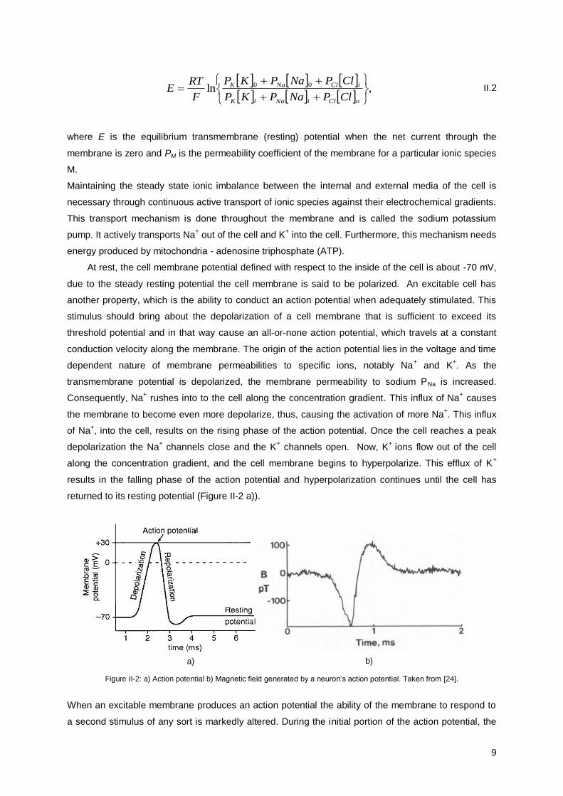


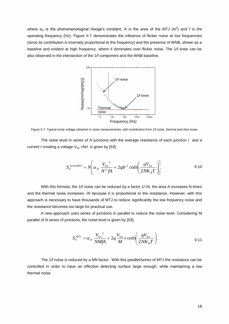


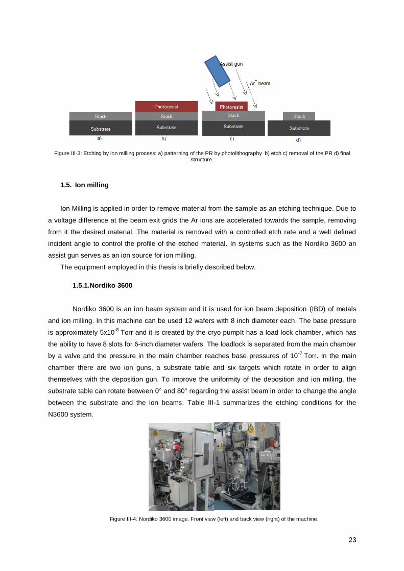

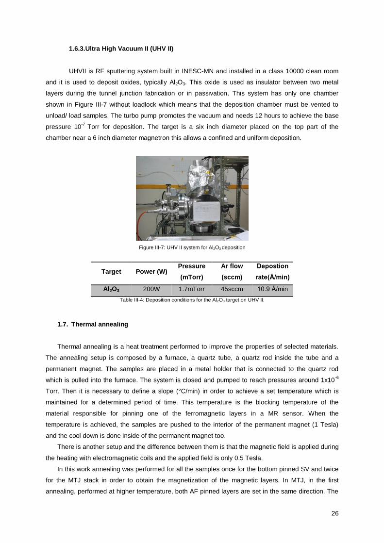

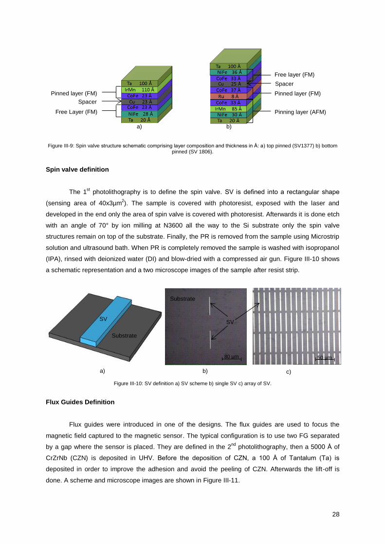
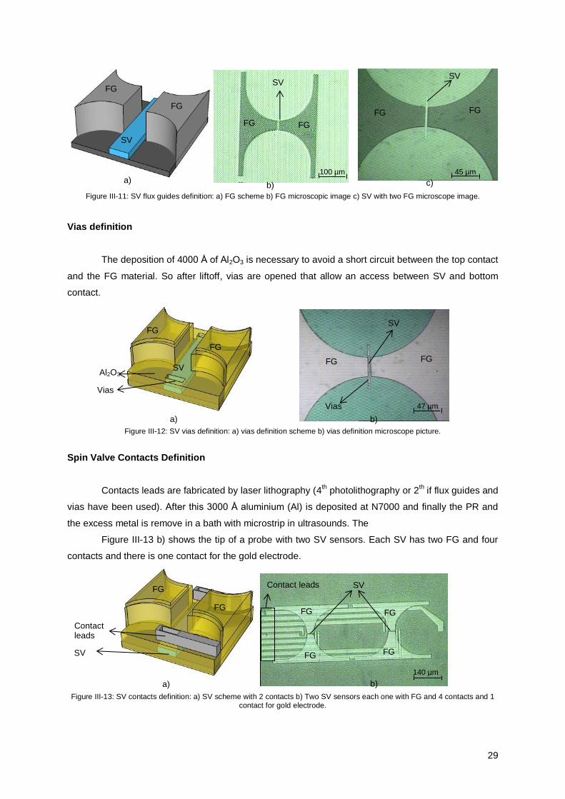
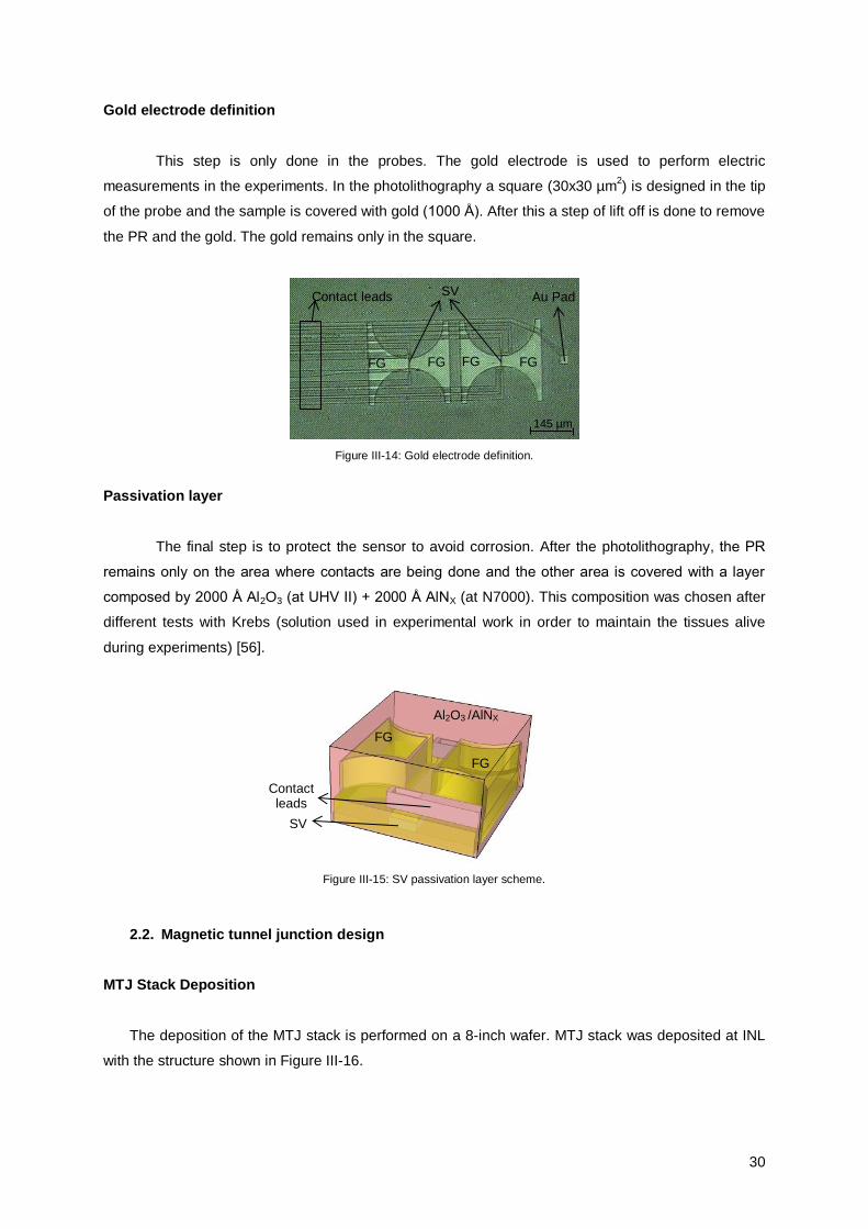

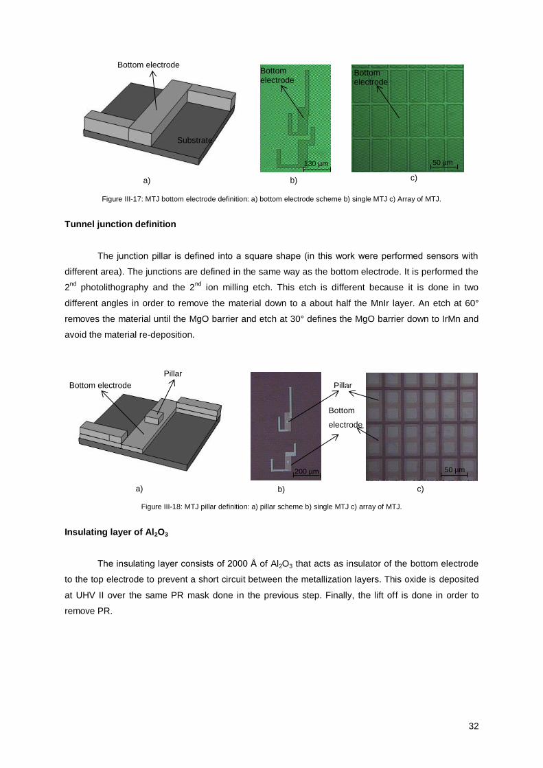


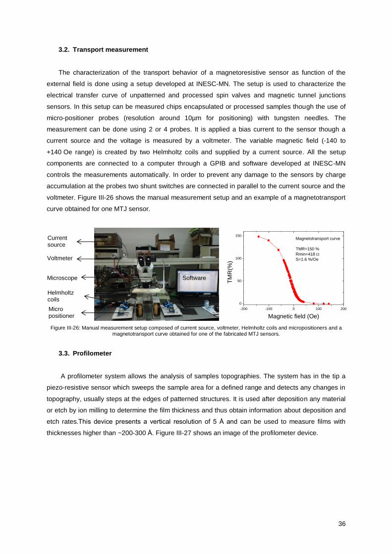
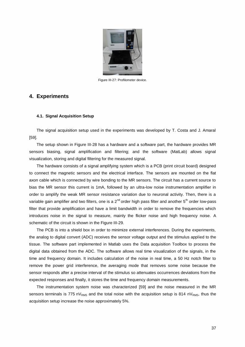
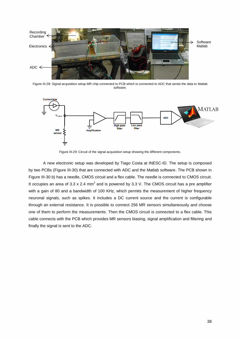
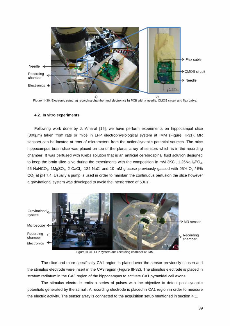


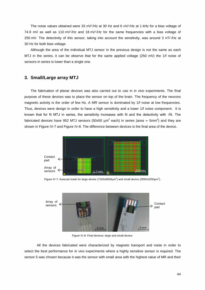
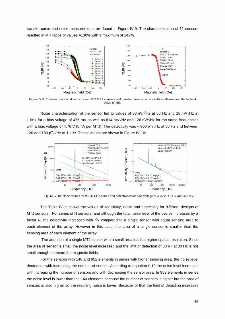
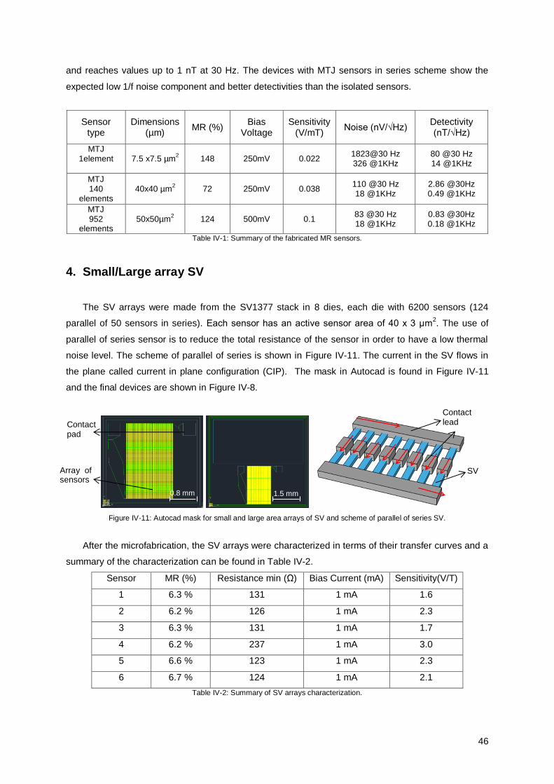

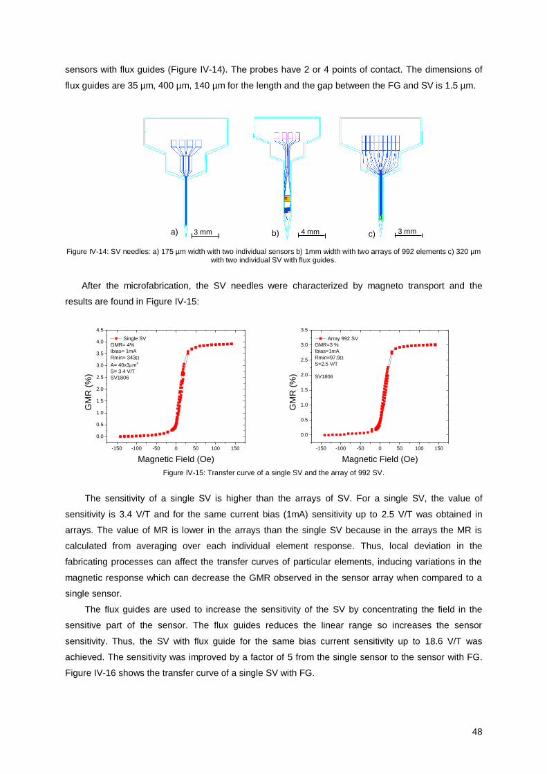
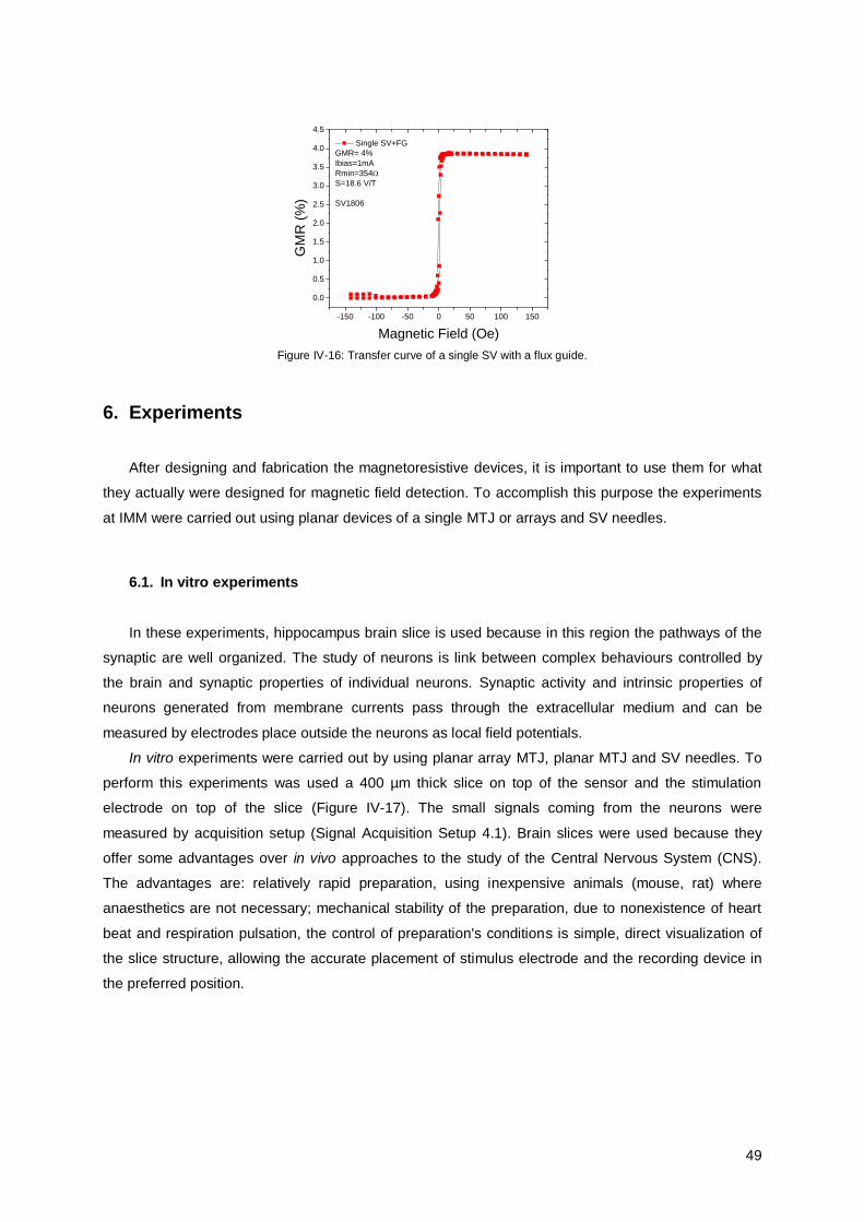
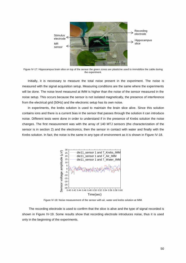

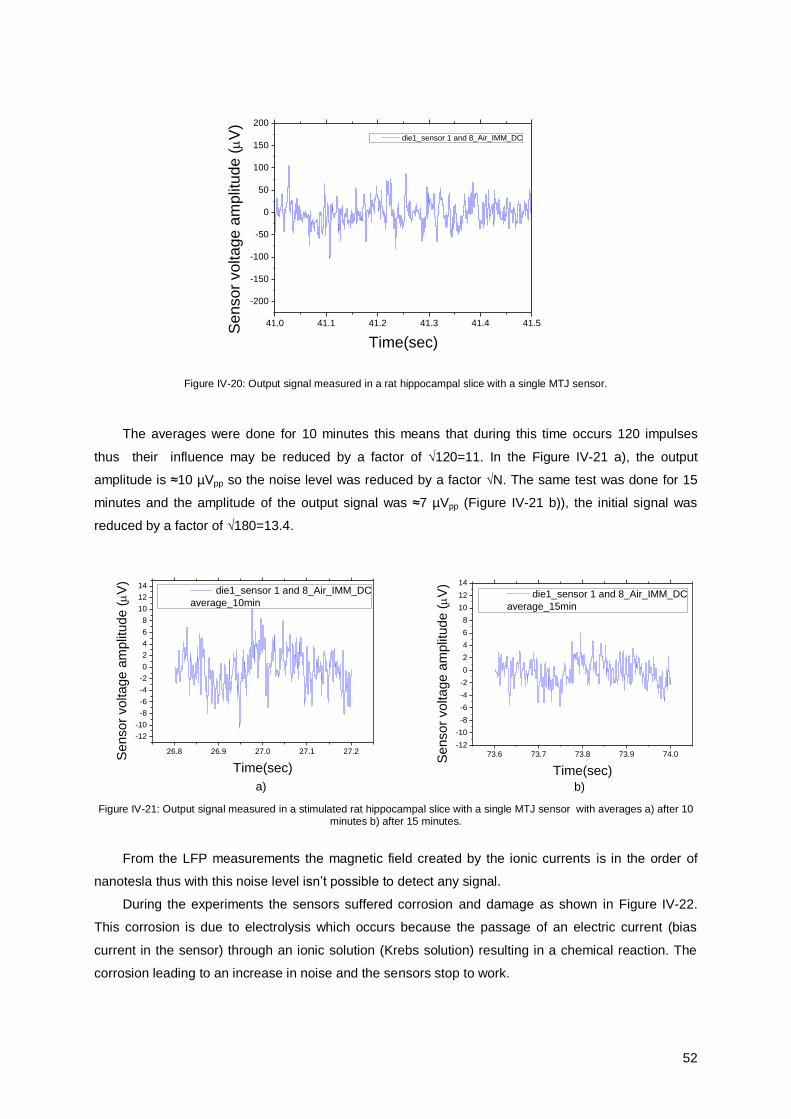
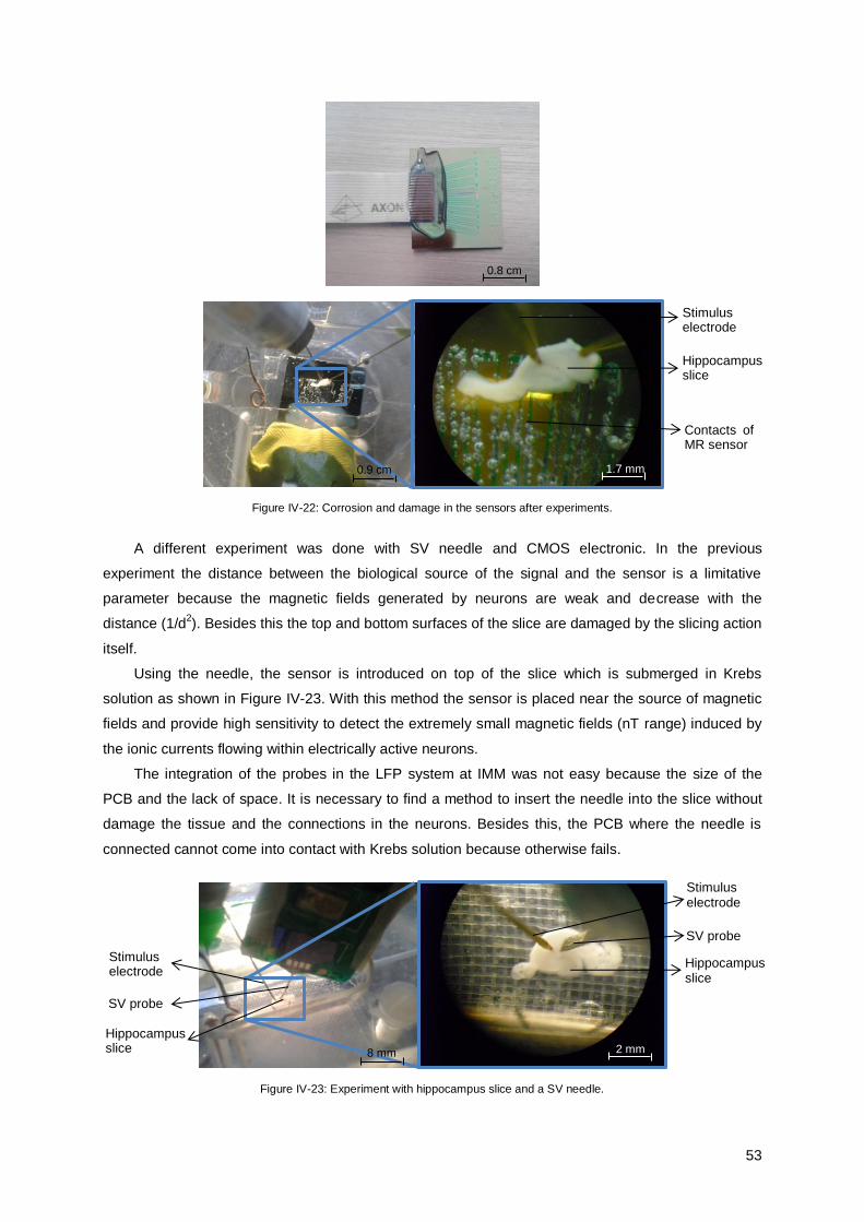


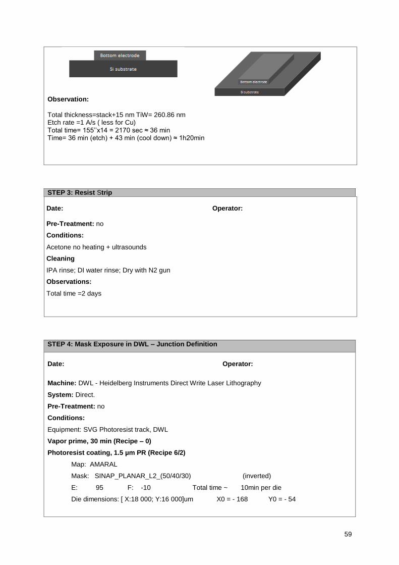
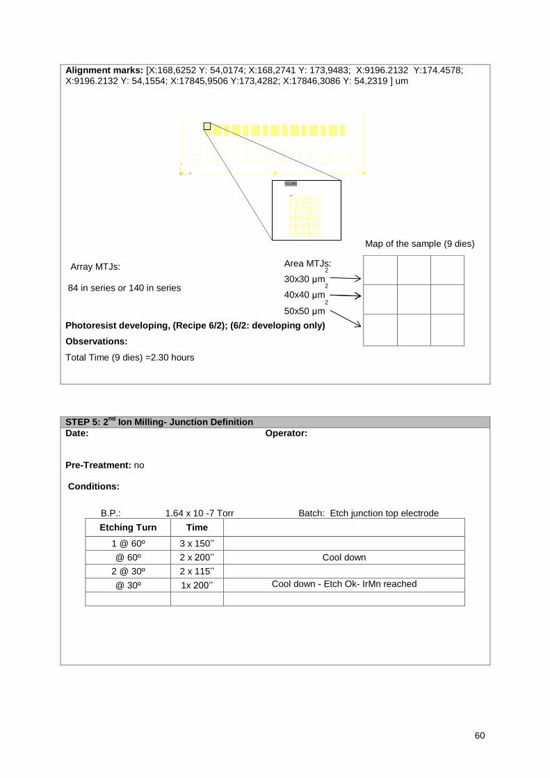
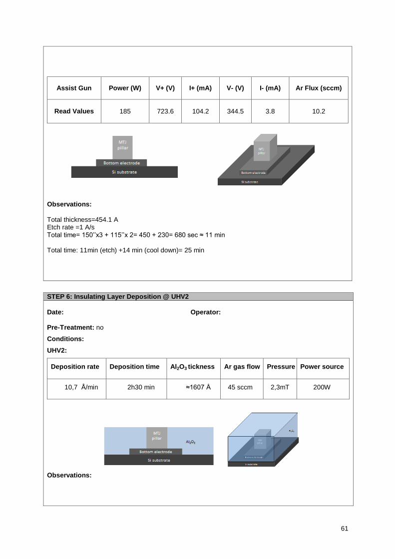
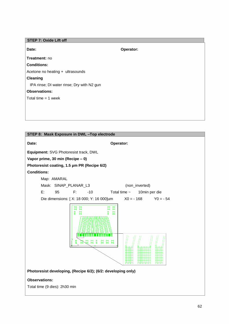

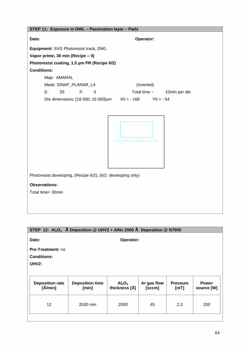

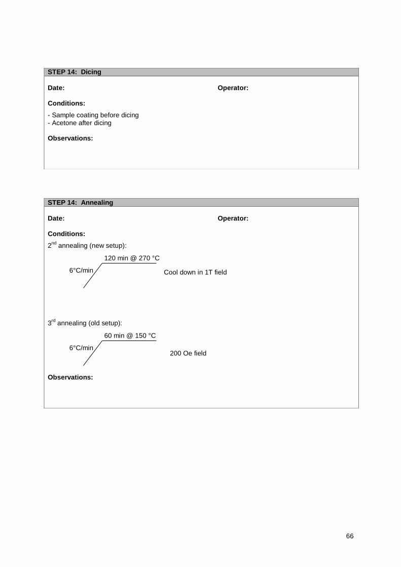
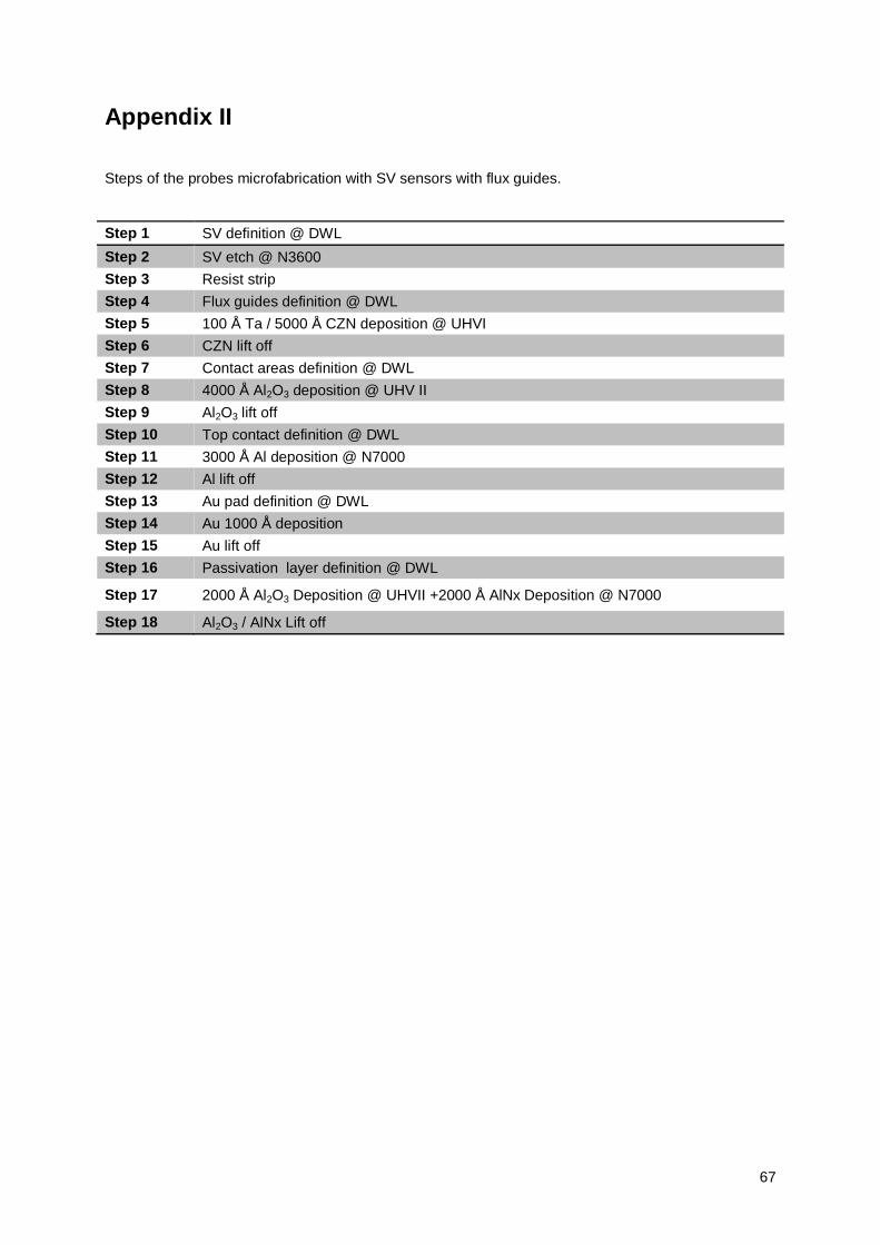


![Untitled-2 [agito-fotos.s3-website-us-east-1.amazonaws.com]agito-fotos.s3-website-us-east-1.amazonaws.com/agitoaraxa/... · 2 fatias de mussarela, bacon, alface, tomate e maionese](https://static.documents.pub/doc/80x56/5c08a38009d3f2603b8c4905/untitled-2-agito-fotoss3-website-us-east-1-agito-fotoss3-website-us-east-1.jpg)


