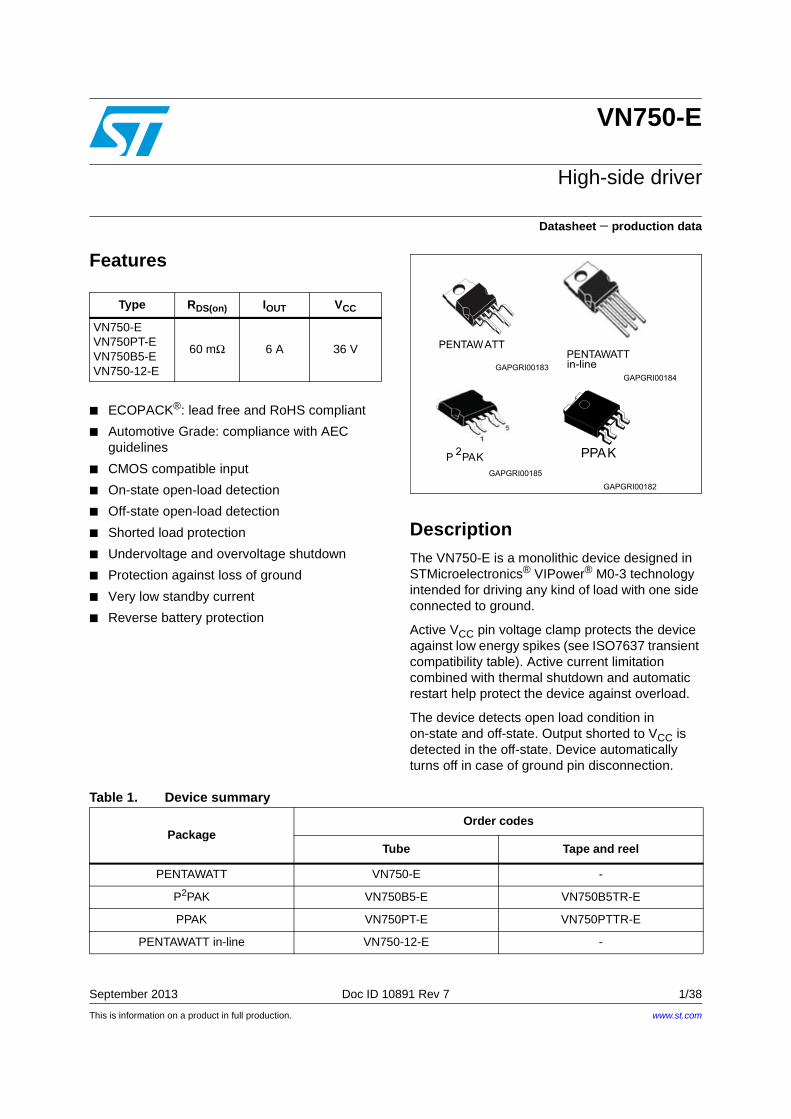
This is information on a product in full production. September 2013 Doc ID 10891 Rev 7 1/38 1 VN750-E High-side driver Datasheet − production data Features ■ ECOPACK ® : lead free and RoHS compliant ■ Automotive Grade: compliance with AEC guidelines ■ CMOS compatible input ■ On-state open-load detection ■ Off-state open-load detection ■ Shorted load protection ■ Undervoltage and overvoltage shutdown ■ Protection against loss of ground ■ Very low standby current ■ Reverse battery protection Description The VN750-E is a monolithic device designed in STMicroelectronics ® VIPower ® M0-3 technology intended for driving any kind of load with one side connected to ground. Active V CC pin voltage clamp protects the device against low energy spikes (see ISO7637 transient compatibility table). Active current limitation combined with thermal shutdown and automatic restart help protect the device against overload. The device detects open load condition in on-state and off-state. Output shorted to V CC is detected in the off-state. Device automatically turns off in case of ground pin disconnection. Type R DS(on) I OUT V CC VN750-E VN750PT-E VN750B5-E VN750-12-E 60 mΩ 6 A 36 V Table 1. Device summary Package Order codes Tube Tape and reel PENTAWATT VN750-E - P 2 PAK VN750B5-E VN750B5TR-E PPAK VN750PT-E VN750PTTR-E PENTAWATT in-line VN750-12-E - www.st.com
Transcript
This is information on a product in full production.
September 2013 Doc ID 10891 Rev 7 1/38
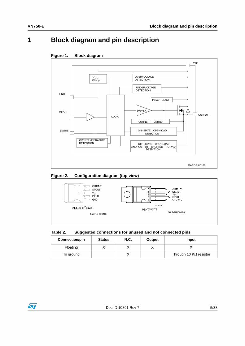
1
VN750-E
High-side driver
Datasheet − production data
Features
■ ECOPACK®: lead free and RoHS compliant
■ Automotive Grade: compliance with AEC guidelines
■ CMOS compatible input
■ On-state open-load detection
■ Off-state open-load detection
■ Shorted load protection
■ Undervoltage and overvoltage shutdown
■ Protection against loss of ground
■ Very low standby current
■ Reverse battery protection
DescriptionThe VN750-E is a monolithic device designed in STMicroelectronics® VIPower® M0-3 technology intended for driving any kind of load with one side connected to ground.
Active VCC pin voltage clamp protects the device against low energy spikes (see ISO7637 transient compatibility table). Active current limitation combined with thermal shutdown and automatic restart help protect the device against overload.
The device detects open load condition in on-state and off-state. Output shorted to VCC is detected in the off-state. Device automatically turns off in case of ground pin disconnection.
Table 2. Suggested connections for unused and not connected pins
Connection/pin Status N.C. Output Input
Floating X X X X
To ground X Through 10 KΩ resistor
Electrical specifications VN750-E
6/38 Doc ID 10891 Rev 7
2 Electrical specifications
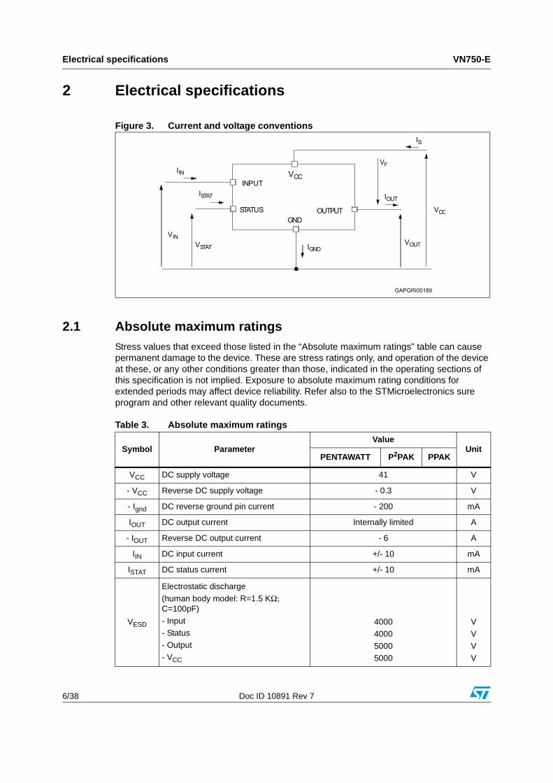
Figure 3. Current and voltage conventions
2.1 Absolute maximum ratingsStress values that exceed those listed in the “Absolute maximum ratings” table can cause permanent damage to the device. These are stress ratings only, and operation of the device at these, or any other conditions greater than those, indicated in the operating sections of this specification is not implied. Exposure to absolute maximum rating conditions for extended periods may affect device reliability. Refer also to the STMicroelectronics sure program and other relevant quality documents.
Table 3. Absolute maximum ratings
Symbol ParameterValue
UnitPENTAWATT P2PAK PPAK
VCC DC supply voltage 41 V
- VCC Reverse DC supply voltage - 0.3 V
- Ignd DC reverse ground pin current - 200 mA
IOUT DC output current Internally limited A
- IOUT Reverse DC output current - 6 A
IIN DC input current +/- 10 mA
ISTAT DC status current +/- 10 mA
VESD
Electrostatic discharge
(human body model: R=1.5 KΩ; C=100pF)
- Input- Status- Output
- VCC
40004000
50005000
VV
VV
VN750-E Electrical specifications
Doc ID 10891 Rev 7 7/38
2.2 Thermal data
2.3 Electrical characteristicsValues specified in this section are for 8 V<VCC<36 V; -40 °C< Tj <150 °C, unless otherwise stated.
EMAX
Maximum switching energy(L=2.46 mH; RL=0 Ω; Vbat=13.5 V; Tjstart=150 °C; IL=9 A)
138 138 mJ
Ptot Power dissipation TC=25°C 60 W
Tj Junction operating temperature Internally limited °C
IL(off1) Off-state output current VIN=VOUT=0 V 0 50 µA
IL(off2) Off-state output current VIN=0V; VOUT=3.5 V -75 0 µA
IL(off3) Off-state output current VIN=VOUT=0 V; Vcc=13 V; Tj =125 °C 5 µA
IL(off4) Off-state output current VIN=VOUT=0 V; Vcc=13 V; Tj =25 °C 3 µA
Switching (VCC=13 V)
td(on) Turn-on delay time RL=6.5 Ω from VIN rising edge to VOUT=1.3 V
40 µs
td(off) Turn-off delay time RL=6.5 Ω from VIN falling edge to VOUT=11.7 V
30 µs
dVOUT/dt(on) Turn-on voltage slopeRL=6.5 Ω from VOUT=1.3 V to VOUT=10.4 V
See Figure 21. V/µs
dVOUT/dt(off) Turn-off voltage slopeRL=6.5 Ω from VOUT=11.7 V to VOUT=1.3 V
See Figure 22. V/µs
Input pin
VIL Input low level 1.25 V
IIL Low level input current VIN=1.25 V 1 µA
VIH Input high level 3.25 V
IIH High level input current VIN=3.25 V 10 µA
Vhyst Input hysteresis voltage 0.5 V
VICL Input clamp voltageIIN=1 mA
IIN=-1 mA6
6.8
-0.7
8 V
V
VCC output diode
VF Forward on voltage -IOUT=1.3 A; Tj=150 °C 0.6 V
Status pin
VSTAT Status low output voltage ISTAT=1.6 mA 0.5 V
ILSTAT Status leakage current Normal operation; VSTAT=5 V 10 µA
CSTATStatus pin input capacitance
Normal operation; VSTAT=5 V 100 pF
VSCL Status clamp voltageISTAT=1mAISTAT=-1mA
6 6.8-0.7
8 VV
Protections(1)
TTSD Shutdown temperature 150 175 200 °C
Table 5. Electrical characteristics (continued)
Symbol Parameter Test conditions Min. Typ. Max. Unit
VN750-E Electrical specifications
Doc ID 10891 Rev 7 9/38
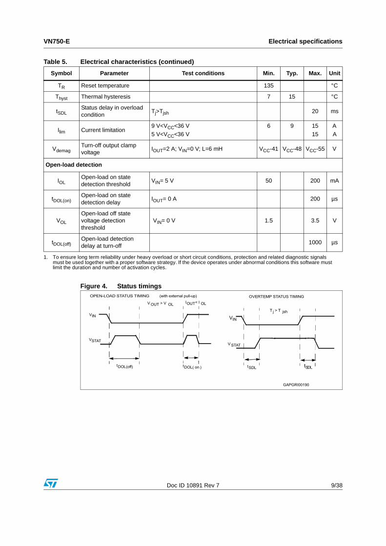
Figure 4. Status timings
TR Reset temperature 135 °C
Thyst Thermal hysteresis 7 15 °C
tSDLStatus delay in overload condition
Tj>Tjsh 20 ms
Ilim Current limitation9 V<VCC<36 V5 V<VCC<36 V
6 9 1515
AA
VdemagTurn-off output clamp voltage
IOUT=2 A; VIN=0 V; L=6 mH VCC-41 VCC-48 VCC-55 V
Open-load detection
IOLOpen-load on state detection threshold
VIN= 5 V 50 200 mA
tDOL(on)Open-load on state detection delay
IOUT= 0 A 200 µs
VOL
Open-load off state voltage detection threshold
VIN= 0 V 1.5 3.5 V
tDOL(off)Open-load detection delay at turn-off
1000 µs
1. To ensure long term reliability under heavy overload or short circuit conditions, protection and related diagnostic signals must be used together with a proper software strategy. If the device operates under abnormal conditions this software must limit the duration and number of activation cycles.
Table 5. Electrical characteristics (continued)
Symbol Parameter Test conditions Min. Typ. Max. Unit
Electrical specifications VN750-E
10/38 Doc ID 10891 Rev 7
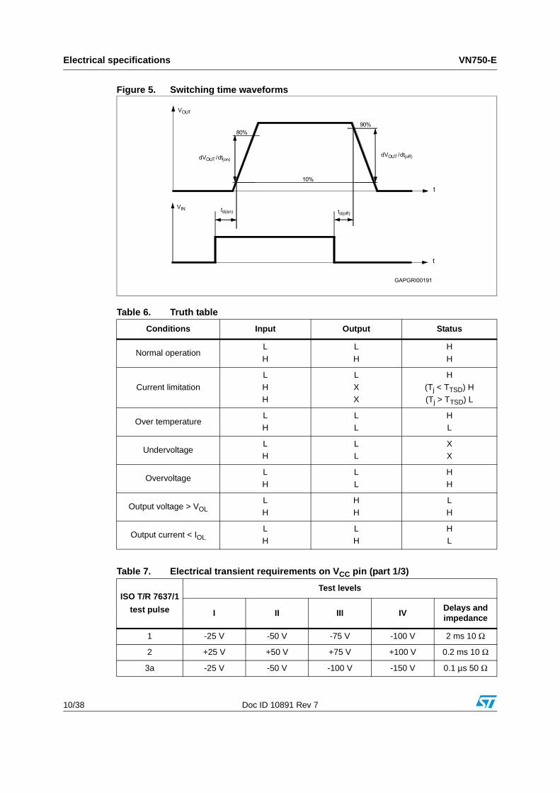
Figure 5. Switching time waveforms
Table 6. Truth table
Conditions Input Output Status
Normal operationL
H
L
H
H
H
Current limitation
L
HH
L
XX
H
(Tj < TTSD) H(Tj > TTSD) L
Over temperatureLH
LL
HL
UndervoltageLH
LL
XX
OvervoltageLH
LL
HH
Output voltage > VOLLH
HH
LH
Output current < IOLLH
LH
HL
Table 7. Electrical transient requirements on VCC pin (part 1/3)
ISO T/R 7637/1
test pulse
Test levels
I II III IVDelays andimpedance
1 -25 V -50 V -75 V -100 V 2 ms 10 Ω
2 +25 V +50 V +75 V +100 V 0.2 ms 10 Ω
3a -25 V -50 V -100 V -150 V 0.1 µs 50 Ω
VN750-E Electrical specifications
Doc ID 10891 Rev 7 11/38
3b +25 V +50 V +75 V +100 V 0.1 µs 50 Ω
4 -4 V -5 V -6 V -7 V 100 ms, 0.01 Ω
5 +26.5 V +46.5 V +66.5 V +86.5 V 400 ms, 2 Ω
Table 8. Electrical transient requirements on VCC pin (part 2/3)
ISO T/R 7637/1
test pulse
Test levels results
I II III IV
1 C C C C
2 C C C C
3a C C C C
3b C C C C
4 C C C C
5 C E E E
Table 9. Electrical transient requirements on VCC pin (part 3/3)
Class Contents
C All functions of the device are performed as designed after exposure to disturbance.
EOne or more functions of the device is not performed as designed after exposure to disturbance and cannot be returned to proper operation without replacing the device.
Figure 21. Turn-on voltage slope Figure 22. Turn-off voltage slope
Figure 23. Ilim Vs Tcase
-50 -25 0 25 50 75 100 125 150 175
Tc (°C)
30
32
34
36
38
40
42
44
46
48
50
Vov (V)
-50 -25 0 25 50 75 100 125 150 175
Tc (ºC)
1
1.5
2
2.5
3
3.5
4
4.5
5
Vol (V)
Vin=0V
-50 -25 0 25 50 75 100 125 150 175
Tc (ºC)
0
100
200
300
400
500
600
700
800
900
1000
dVout/dt/(on) (V/ms)
Vcc=13VRl=6.5Ohm
-50 -25 0 25 50 75 100 125 150 175
Tc (ºC)
0
50
100
150
200
250
300
350
400
450
500
dVout/dt(off) (V/ms)
Vcc=13V Rl=6.5Ohm
-50 -25 0 25 50 75 100 125 150 175
Tc (ºC)
0
2
4
6
8
10
12
14
16
18
20
Ilim (A)
Vcc=13V
Electrical specifications VN750-E
16/38 Doc ID 10891 Rev 7
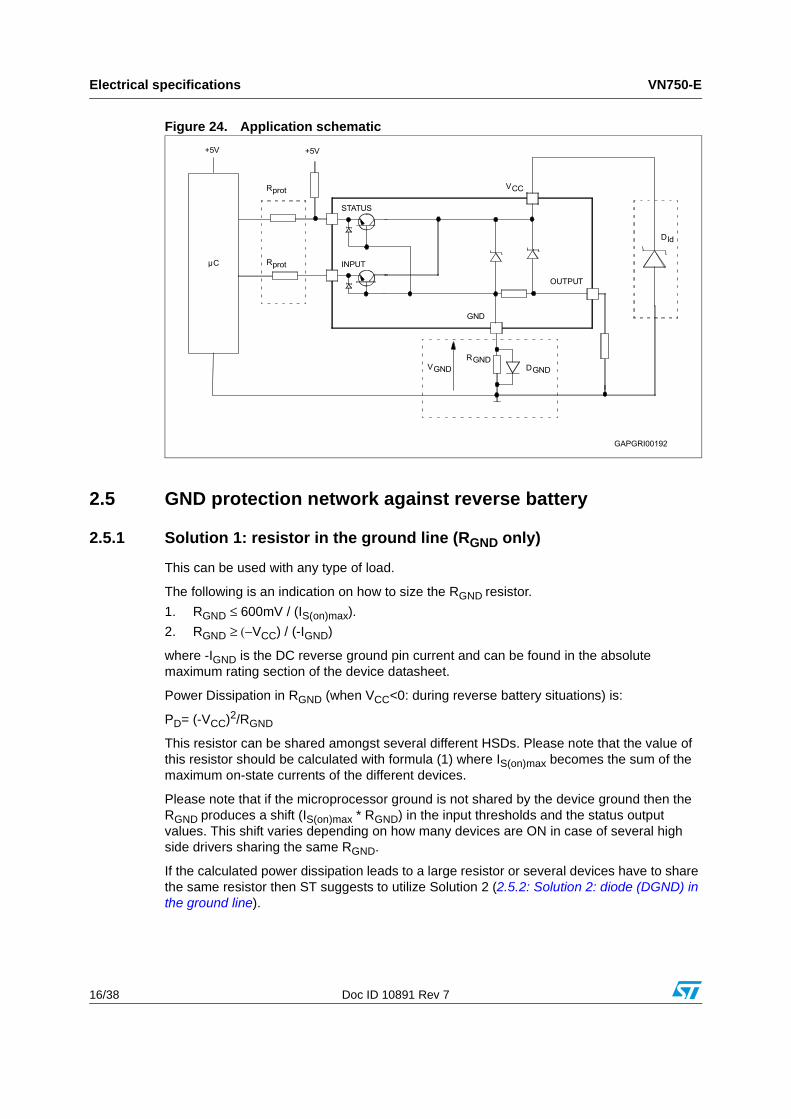
Figure 24. Application schematic
2.5 GND protection network against reverse battery
2.5.1 Solution 1: resistor in the ground line (RGND only)
This can be used with any type of load.
The following is an indication on how to size the RGND resistor.
1. RGND ≤ 600mV / (IS(on)max).
2. RGND ≥ (−VCC) / (-IGND)
where -IGND is the DC reverse ground pin current and can be found in the absolute maximum rating section of the device datasheet.
Power Dissipation in RGND (when VCC<0: during reverse battery situations) is:
PD= (-VCC)2/RGND
This resistor can be shared amongst several different HSDs. Please note that the value of this resistor should be calculated with formula (1) where IS(on)max becomes the sum of the maximum on-state currents of the different devices.
Please note that if the microprocessor ground is not shared by the device ground then the RGND produces a shift (IS(on)max * RGND) in the input thresholds and the status output values. This shift varies depending on how many devices are ON in case of several high side drivers sharing the same RGND.
If the calculated power dissipation leads to a large resistor or several devices have to share the same resistor then ST suggests to utilize Solution 2 (2.5.2: Solution 2: diode (DGND) in the ground line).
VN750-E Electrical specifications
Doc ID 10891 Rev 7 17/38
2.5.2 Solution 2: diode (DGND) in the ground line
A resistor (RGND=1 kΩ) should be inserted in parallel to DGND if the device drives an inductive load.
This small signal diode can be safely shared amongst several different HSDs. Also in this case, the presence of the ground network produces a shift (≈600mV) in the input threshold and in the status output values if the microprocessor ground is not common to the device ground. This shift does not vary if more than one HSD shares the same diode/resistor network.
Series resistor in input and status lines are also required to prevent that, during battery voltage transient, the current exceeds the absolute maximum rating.
The safest configuration for unused input and status pin is to leave them unconnected.
2.6 Load dump protection Dld is necessary (voltage transient suppressor) if the load dump peak voltage exceeds the VCC max DC rating. The same applies if the device is subject to transients on the VCC line that are greater than the ones shown in the ISO 7637-2: 2004(E) table.
2.7 Microcontroller I/Os protectionIf a ground protection network is used and negative transient are present on the VCC line, the control pins are pulled negative. ST suggests to insert a resistor (Rprot) in line to prevent the µC I/Os pins to latch-up.
The value of these resistors is a compromise between the leakage current of µC and the current required by the HSD I/Os (Input levels compatibility) with from latching-up limit of µC I/Os.
For VCCpeak= - 100 V and Ilatchup ≥ 20 mA; VOHµC ≥ 4.5 V
5 kΩ ≤ Rprot ≤ 65 kΩ.
Recommended values: Rprot =10 kΩ.
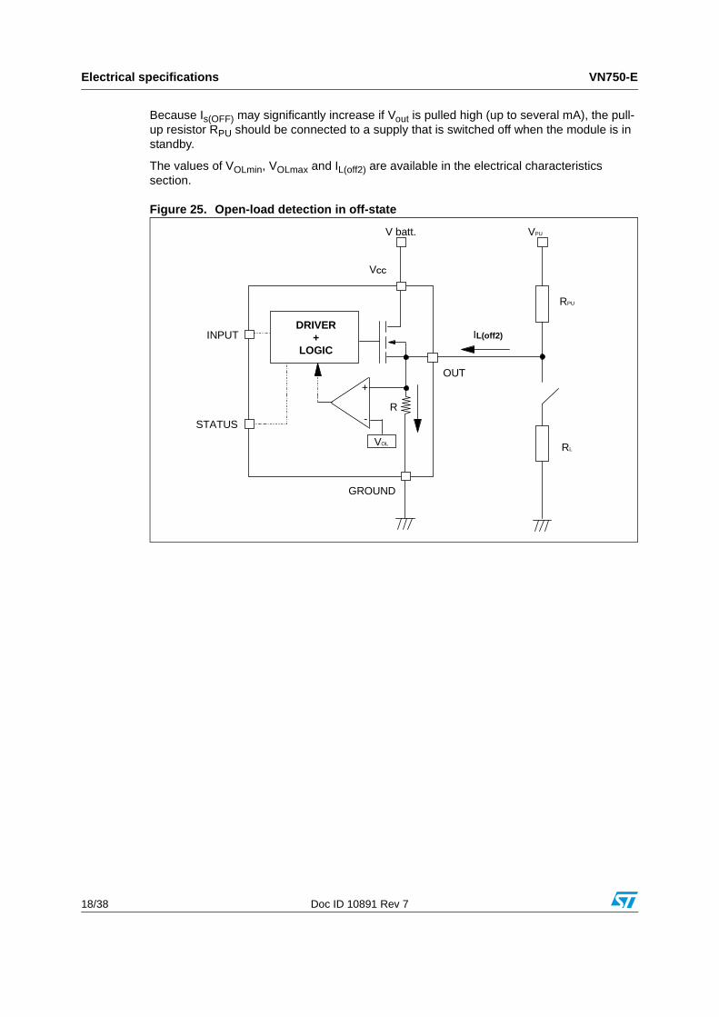
2.8 Open-load detection in off-stateOff-state open-load detection requires an external pull-up resistor (RPU) connected between output pin and a positive supply voltage (VPU) like the +5 V line used to supply the microprocessor.
The external resistor has to be selected according to the following requirements:
1. no false open-load indication when load is connected: in this case we have to avoid VOUT to be higher than VOlmin; this results in the following conditionVOUT=(VPU/(RL+RPU))RL<VOlmin.
2. no misdetection when load is disconnected: in this case the VOUT has to be higher than VOLmax; this results in the following condition RPU<(VPU–VOLmax)/IL(off2).
Electrical specifications VN750-E
18/38 Doc ID 10891 Rev 7
Because Is(OFF) may significantly increase if Vout is pulled high (up to several mA), the pull-up resistor RPU should be connected to a supply that is switched off when the module is in standby.
The values of VOLmin, VOLmax and IL(off2) are available in the electrical characteristics section.
Figure 25. Open-load detection in off-state
VOL
V batt. VPU
RPU
RL
R
DRIVER +
LOGIC
+
-
INPUT
STATUS
VCC
OUT
GROUND
IL(off2)
VN750-E Electrical specifications
Doc ID 10891 Rev 7 19/38
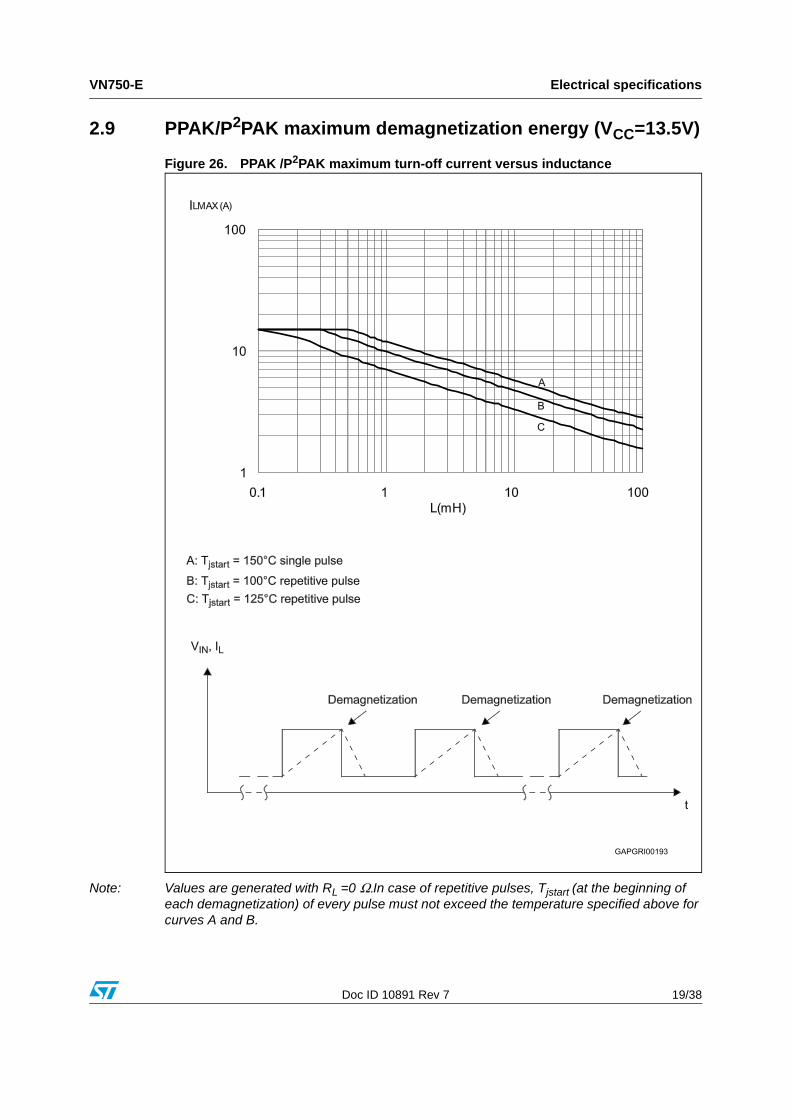
2.9 PPAK/P2PAK maximum demagnetization energy (VCC=13.5V)
Figure 26. PPAK /P2PAK maximum turn-off current versus inductance
Note: Values are generated with RL =0 Ω.In case of repetitive pulses, Tjstart (at the beginning of each demagnetization) of every pulse must not exceed the temperature specified above for curves A and B.
Package and PCB thermal data VN750-E
20/38 Doc ID 10891 Rev 7
3 Package and PCB thermal data
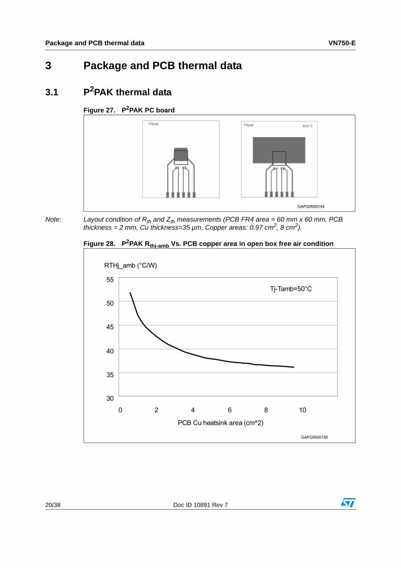
3.1 P2PAK thermal data
Figure 27. P2PAK PC board
Note: Layout condition of Rth and Zth measurements (PCB FR4 area = 60 mm x 60 mm, PCB thickness = 2 mm, Cu thickness=35 µm, Copper areas: 0.97 cm2, 8 cm2).
Figure 28. P2PAK Rthj-amb Vs. PCB copper area in open box free air condition
GAPGRI00194
VN750-E Package and PCB thermal data
Doc ID 10891 Rev 7 21/38
Figure 29. P2PAK thermal impedance junction ambient single pulse
Equation 1: pulse calculation formula
where δ = tP/T
Figure 30. P2PAK thermal fitting model of a single channel
ZTHδ RTH δ ZTHtp 1 δ–( )+⋅=
GAPGRI00197
Package and PCB thermal data VN750-E
22/38 Doc ID 10891 Rev 7
3.2 PPAK thermal data
Figure 31. PPAK PC board
Note: Layout condition of Rth and Zth measurements (PCB FR4 area = 60 mm x 60 mm, PCB thickness = 2 mm, Cu thickness=35 µm, Copper areas: 0.44 cm2, 8 cm2).
Table 10. P2PAK thermal parameter
Area/island (cm2) 0.5 6
R1 (°C/W) 0.15
R2 (°C/W) 0.7
R3 (°C/W) 0.7
R4 (°C/W) 4
R5 (°C/W) 9
R6 (°C/W) 37 22
C1 (W·s/°C) 0.0006
C2 (W·s/°C) 0.0025
C3 (W·s/°C) 0.055
C4 (W·s/°C) 0.4
C5 (W·s/°C) 2
C6 (W·s/°C) 3 5
GAPGRI00172
VN750-E Package and PCB thermal data
Doc ID 10891 Rev 7 23/38
Figure 32. PPAK Rthj-amb Vs. PCB copper area in open box free air condition
Figure 33. PPAK thermal impedance junction ambient single pulse
Package and PCB thermal data VN750-E
24/38 Doc ID 10891 Rev 7
Equation 2: pulse calculation formula
where δ = tP/T
Figure 34. PPAK thermal fitting model of a single channel
Table 11. PPAK thermal parameter
Area/island (cm2) 0.5 6
R1 (°C/W) 0.15
R2 (°C/W) 0.7
R3 (°C/W) 1.6
R4 (°C/W) 2
R5 (°C/W) 15
R6 (°C/W) 61 24
C1 (W·s/°C) 0.0006
C2 (W·s/°C) 0.0025
C3 (W·s/°C) 0.08
C4 (W·s/°C) 0.3
C5 (W·s/°C) 0.45
C6 (W·s/°C) 0.8 5
ZTHδ RTH δ ZTHtp 1 δ–( )+⋅=
GAPGRI00200
VN750-E Package and packing information
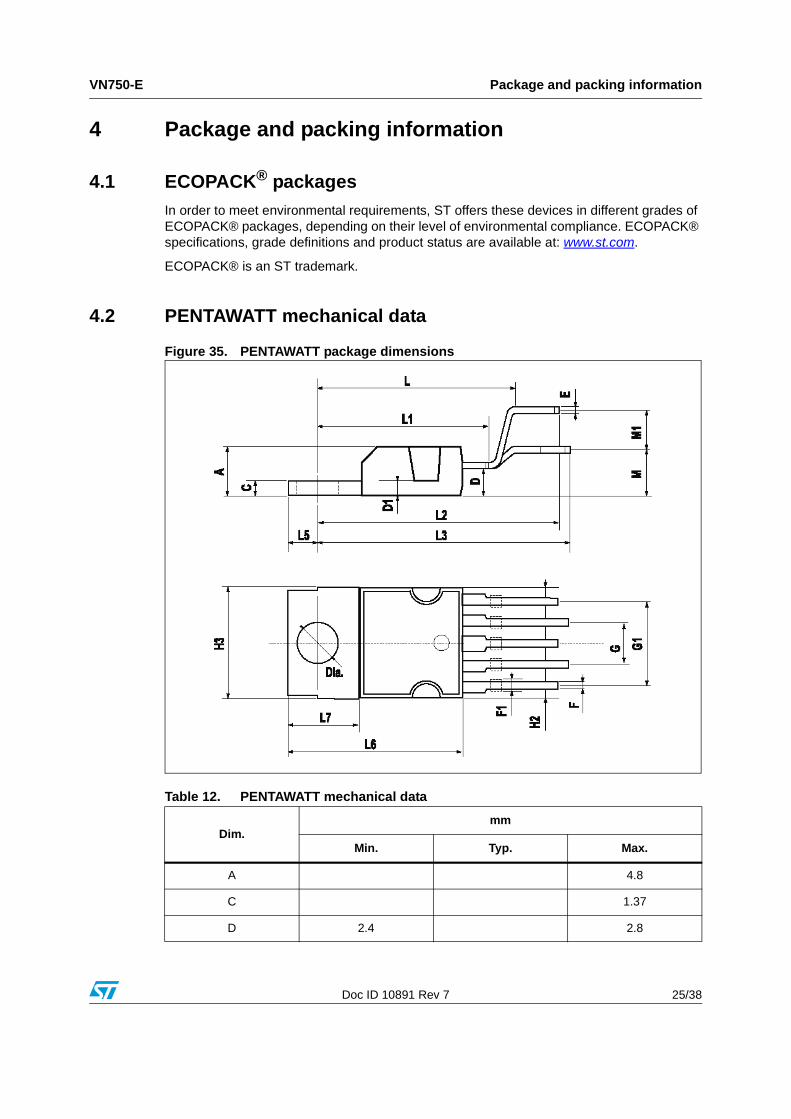
Doc ID 10891 Rev 7 25/38
4 Package and packing information
4.1 ECOPACK® packagesIn order to meet environmental requirements, ST offers these devices in different grades of ECOPACK® packages, depending on their level of environmental compliance. ECOPACK® specifications, grade definitions and product status are available at: www.st.com.
Table 13. PENTAWATT (in-line) mechanical data (continued)
Symbolmillimeters
Min Typ Max
VN750-E Package and packing information
Doc ID 10891 Rev 7 29/38
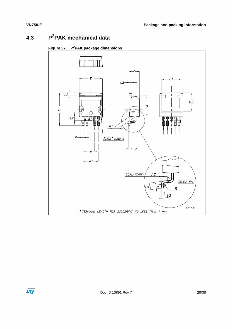
4.3 P2PAK mechanical data
Figure 37. P2PAK package dimensions
P010R
Package and packing information VN750-E
30/38 Doc ID 10891 Rev 7
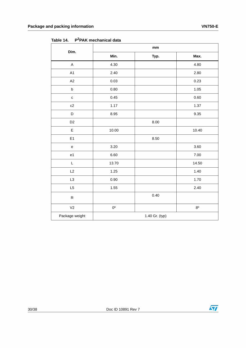
Table 14. P2PAK mechanical data
Dim.mm
Min. Typ. Max.
A 4.30 4.80
A1 2.40 2.80
A2 0.03 0.23
b 0.80 1.05
c 0.45 0.60
c2 1.17 1.37
D 8.95 9.35
D2 8.00
E 10.00 10.40
E1 8.50
e 3.20 3.60
e1 6.60 7.00
L 13.70 14.50
L2 1.25 1.40
L3 0.90 1.70
L5 1.55 2.40
R0.40
V2 0º 8º
Package weight 1.40 Gr. (typ)
VN750-E Package and packing information
Doc ID 10891 Rev 7 31/38
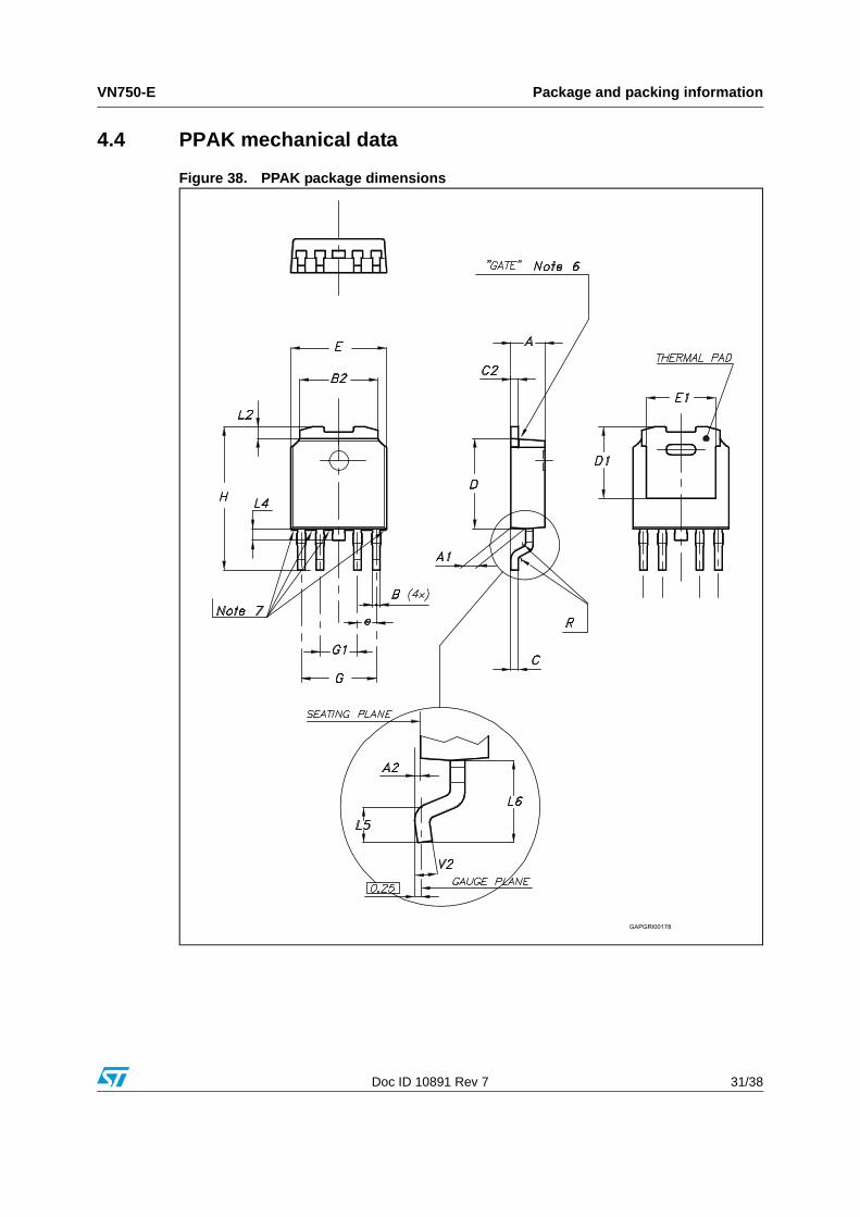
4.4 PPAK mechanical data
Figure 38. PPAK package dimensions
Package and packing information VN750-E
32/38 Doc ID 10891 Rev 7
Table 15. PPAK mechanical data
Dim.mm
Min. Typ. Max.
A 2.20 2.40
A1 0.90 1.10
A2 0.03 0.23
B 0.40 0.60
B2 5.20 5.40
C 0.45 0.60
C2 0.48 0.60
D1 5.1
D 6.00 6.20
E 6.40 6.60
E1 4.7
e 1.27
G 4.90 5.25
G1 2.38 2.70
H 9.35 10.10
L2 0.8 1.00
L4 0.60 1.00
L5 1
L6 2.80
R 0.2
V2 0º 8º
Package weight Gr. 0.3
VN750-E Package and packing information
Doc ID 10891 Rev 7 33/38
4.5 PENTAWATT packing informationThe devices can be packed in tube or tape and reel shipments (see the Device summary on page 1).
Figure 39. PENTAWATT tube shipment (no suffix)
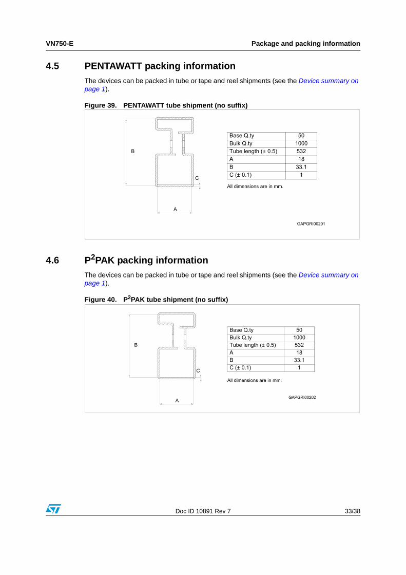
4.6 P2PAK packing informationThe devices can be packed in tube or tape and reel shipments (see the Device summary on page 1).
Figure 40. P2PAK tube shipment (no suffix)
Package and packing information VN750-E
34/38 Doc ID 10891 Rev 7
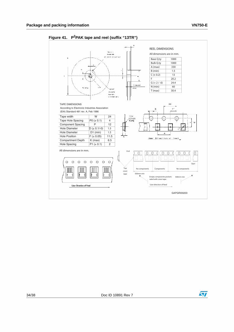
Figure 41. P2PAK tape and reel (suffix “13TR”)
TAPE DIMENSIONS
According to Electronic Industries Association
(EIA) Standard 481 rev. A, Feb 1986
All dimensions are in mm.
Tape width W 24Tape Hole Spacing P0 (± 0.1) 4Component Spacing P 12
Hole Diameter D (± 0.1/-0) 1.5
Hole Diameter D1 (min) 1.5
Hole Position F (± 0.05) 11.5Compartment Depth K (max) 6.5Hole Spacing P1 (± 0.1) 2
Top
cover
tape
End
Start
No componentsNo components Components
500mm min
500mm minEmpty components pockets
saled with cover tape.
User direction of feed
REEL DIMENSIONS
All dimensions are in mm.
Base Q.ty 1000
Bulk Q.ty 1000
A (max) 330
B (min) 1.5
C (± 0.2) 13
F 20.2
G (+ 2 / -0) 24.4
N (min) 60
T (max) 30.4
GAPGRI00203
VN750-E Package and packing information
Doc ID 10891 Rev 7 35/38
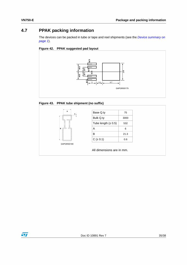
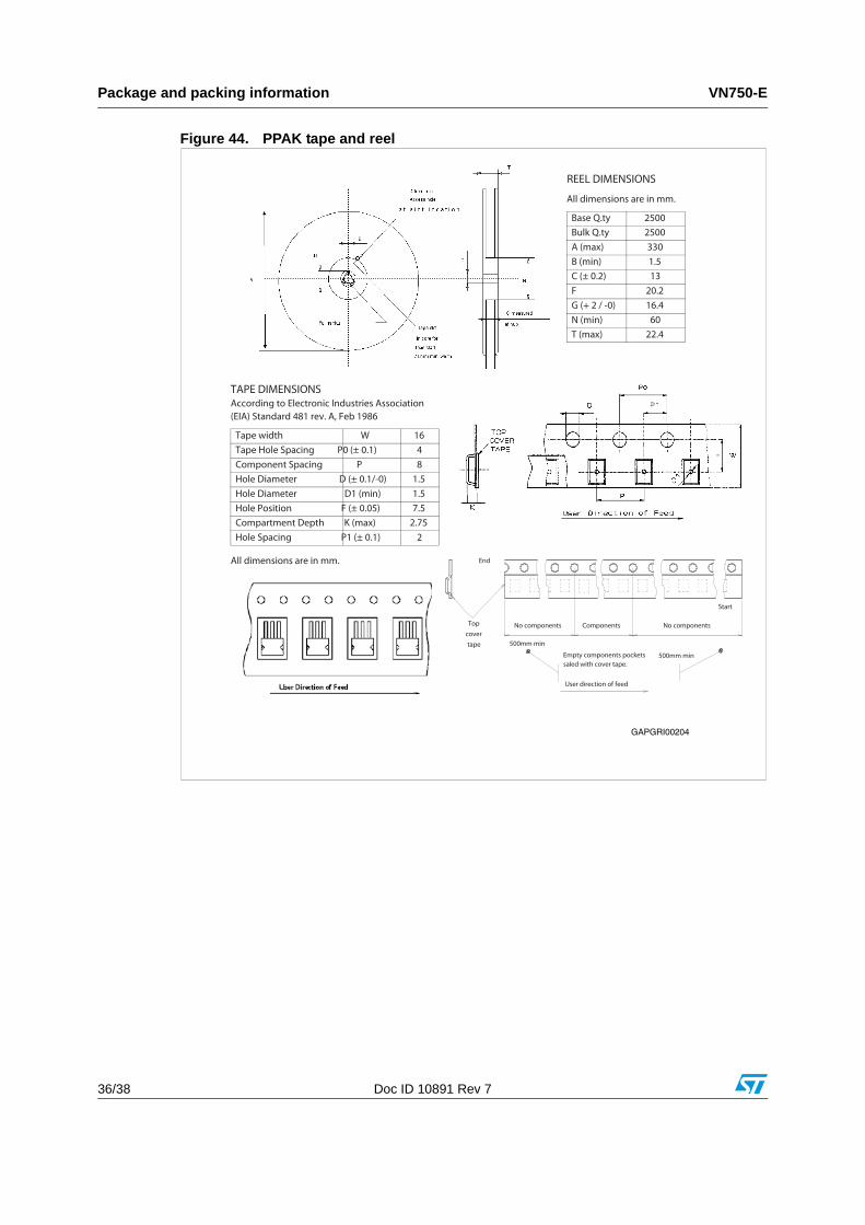
4.7 PPAK packing informationThe devices can be packed in tube or tape and reel shipments (see the Device summary on page 1).
Figure 42. PPAK suggested pad layout
Figure 43. PPAK tube shipment (no suffix)
All dimensions are in mm.
Base Q.ty 75
Bulk Q.ty 3000
Tube length (± 0.5) 532
A 6
B 21.3
C (± 0.1) 0.6
Package and packing information VN750-E
36/38 Doc ID 10891 Rev 7
Figure 44. PPAK tape and reel
All dimensions are in mm.
Base Q.ty 2500
Bulk Q.ty 2500
A (max) 330
B (min) 1.5
C (± 0.2) 13
F 20.2
G (+ 2 / -0) 16.4
N (min) 60
T (max) 22.4
TAPE DIMENSIONSAccording to Electronic Industries Association
(EIA) Standard 481 rev. A, Feb 1986
All dimensions are in mm.
Tape width W 16
Tape Hole Spacing P0 (± 0.1) 4
Component Spacing P 8
Hole Diameter D (± 0.1/-0) 1.5
Hole Diameter D1 (min) 1.5
Hole Position F (± 0.05) 7.5
Compartment Depth K (max) 2.75
Hole Spacing P1 (± 0.1) 2
Top
cover
tape
End
Start
No componentsNo components Components
500mm min
500mm minEmpty components pockets
saled with cover tape.
User direction of feed
REEL DIMENSIONS
GAPGRI00204
VN750-E Revision history
Doc ID 10891 Rev 7 37/38
5 Revision history
Table 16. Document revision history
Date Revision Changes
07-Oct-2004 1 Initial release.
24-Nov-2008 2
Document reformatted and restructured.Added content, list of figures and tables.Added ECOPACK® packages information.
Updated Figure 41: P2PAK tape and reel (suffix “13TR”):– changed component spacing (P) in tape dimensions table from 16
mm to 12 mm.
12-May-2009 3
Removed SO-8 package into the following tables:
Table 1, Table 3 and Table 4.Figure 2: Removed SO-8 package top view.Removed SO-8 package information in the following sections:
Section Note:: Values are generated with RL =0 W.In case of repetitive pulses, Tjstart (at the beginning of each demagnetization) of every pulse must not exceed the temperature specified above for curves A and B. andSection 4: Package and packing informationModified Section 2.1: Absolute maximum ratings and Section 4.1: ECOPACK® packages.
23-Nov-2009 4
Updated features list.
Added PENTAWATT in-line package into the document:– Updated Table 1: Device summary– Added Section 4.2.1: PENTAWATT (in-line) mechanical data.
17-Nov-2010 5Updated following tables:– Table 3: Absolute maximum ratings
– Table 4: Thermal data
11-May-2012 6– Update entire document following ST template.
– Update Table 15 and Figure 38.
19-Sep-2013 7 Updated Disclaimer.
VN750-E
38/38 Doc ID 10891 Rev 7
Please Read Carefully:
Information in this document is provided solely in connection with ST products. STMicroelectronics NV and its subsidiaries (“ST”) reserve theright to make changes, corrections, modifications or improvements, to this document, and the products and services described herein at anytime, without notice.
All ST products are sold pursuant to ST’s terms and conditions of sale.
Purchasers are solely responsible for the choice, selection and use of the ST products and services described herein, and ST assumes noliability whatsoever relating to the choice, selection or use of the ST products and services described herein.
No license, express or implied, by estoppel or otherwise, to any intellectual property rights is granted under this document. If any part of thisdocument refers to any third party products or services it shall not be deemed a license grant by ST for the use of such third party productsor services, or any intellectual property contained therein or considered as a warranty covering the use in any manner whatsoever of suchthird party products or services or any intellectual property contained therein.
UNLESS OTHERWISE SET FORTH IN ST’S TERMS AND CONDITIONS OF SALE ST DISCLAIMS ANY EXPRESS OR IMPLIED WARRANTY WITH RESPECT TO THE USE AND/OR SALE OF ST PRODUCTS INCLUDING WITHOUT LIMITATION IMPLIED WARRANTIES OF MERCHANTABILITY, FITNESS FOR A PARTICULAR PURPOSE (AND THEIR EQUIVALENTS UNDER THE LAWS OF ANY JURISDICTION), OR INFRINGEMENT OF ANY PATENT, COPYRIGHT OR OTHER INTELLECTUAL PROPERTY RIGHT.
ST PRODUCTS ARE NOT DESIGNED OR AUTHORIZED FOR USE IN: (A) SAFETY CRITICAL APPLICATIONS SUCH AS LIFE SUPPORTING, ACTIVE IMPLANTED DEVICES OR SYSTEMS WITH PRODUCT FUNCTIONAL SAFETY REQUIREMENTS; (B) AERONAUTIC APPLICATIONS; (C) AUTOMOTIVE APPLICATIONS OR ENVIRONMENTS, AND/OR (D) AEROSPACE APPLICATIONS OR ENVIRONMENTS. WHERE ST PRODUCTS ARE NOT DESIGNED FOR SUCH USE, THE PURCHASER SHALL USE PRODUCTS AT PURCHASER’S SOLE RISK, EVEN IF ST HAS BEEN INFORMED IN WRITING OF SUCH USAGE, UNLESS A PRODUCT IS EXPRESSLY DESIGNATED BY ST AS BEING INTENDED FOR “AUTOMOTIVE, AUTOMOTIVE SAFETY OR MEDICAL” INDUSTRY DOMAINS ACCORDING TO ST PRODUCT DESIGN SPECIFICATIONS. PRODUCTS FORMALLY ESCC, QML OR JAN QUALIFIED ARE DEEMED SUITABLE FOR USE IN AEROSPACE BY THE CORRESPONDING GOVERNMENTAL AGENCY.
Resale of ST products with provisions different from the statements and/or technical features set forth in this document shall immediately voidany warranty granted by ST for the ST product or service described herein and shall not create or extend in any manner whatsoever, anyliability of ST.
ST and the ST logo are trademarks or registered trademarks of ST in various countries.Information in this document supersedes and replaces all information previously supplied.
The ST logo is a registered trademark of STMicroelectronics. All other names are the property of their respective owners.
Australia - Belgium - Brazil - Canada - China - Czech Republic - Finland - France - Germany - Hong Kong - India - Israel - Italy - Japan - Malaysia - Malta - Morocco - Philippines - Singapore - Spain - Sweden - Switzerland - United Kingdom - United States of America