High-speed growth of TiO 2 nanotube arrays with gradient pore diameter and ultrathin tube wall under high-field anodization This article has been downloaded from IOPscience. Please scroll down to see the full text article. 2010 Nanotechnology 21 405302 (http://iopscience.iop.org/0957-4484/21/40/405302) Download details: IP Address: 202.120.52.96 The article was downloaded on 22/10/2010 at 09:13 Please note that terms and conditions apply. View the table of contents for this issue, or go to the journal homepage for more Home Search Collections Journals About Contact us My IOPscience
Transcript
High-speed growth of TiO2 nanotube arrays with gradient pore diameter and ultrathin tube
wall under high-field anodization
This article has been downloaded from IOPscience. Please scroll down to see the full text article.
High-speed growth of TiO2 nanotubearrays with gradient pore diameter andultrathin tube wall under high-fieldanodizationXiaoliang Yuan1,2, Maojun Zheng1,2,4, Li Ma3 andWenzhong Shen1,2
1 Key Laboratory of Artificial Structures and Quantum Control, Ministry of Education,Department of Physics, Shanghai Jiao Tong University, Shanghai 200240,People’s Republic of China2 Laboratory of Condensed Matter Spectroscopy and Opto-Electronic Physics, Department ofPhysics, Shanghai Jiao Tong University, Shanghai 200240, People’s Republic of China3 School of Chemistry and Chemical Technology, Shanghai Jiao Tong University,Shanghai 200240, People’s Republic of China
Received 19 June 2010, in final form 10 August 2010Published 10 September 2010Online at stacks.iop.org/Nano/21/405302
AbstractHighly ordered TiO2 nanotubular arrays have been prepared by two-step anodization under highfield. The high anodizing current densities lead to a high-speed film growth(0.40–1.00 µm min−1), which is nearly 16 times faster than traditional fabrication of TiO2 atlow field. It was found that an annealing process of Ti foil is an effective approach to get amonodisperse and double-pass TiO2 nanotubular layer with a gradient pore diameter andultrathin tube wall (nearly 10 nm). A higher anodic voltage and longer anodization time arebeneficial to the formation of ultrathin tube walls. This approach is simple and cost-effective infabricating high-quality ordered TiO2 nanotubular arrays for practical applications.
(Some figures in this article are in colour only in the electronic version)
1. Introduction
In recent years, nanotubular materials have attracted increasingattention due to their unique properties and potentialapplications [1–3]. The different chemical and physicalproperties of these novel materials have been ascribed totheir characteristic structural features, that is, high surface-to-volume ratios and size-dependent properties. In particular,much more recent studies have indicated that orderedTiO2 nanotube arrays possess outstanding charge transportproperties. So this outstanding properties had enabled avariety of advanced applications in gas sensing [4], dye-sensitized solar cells [5–10], catalysis [11–14], doping [15],biomedicine [16] and photovoltaics [17–19]. In recent years,there have been many reports on the synthesis strategies of
4 Author to whom any correspondence should be addressed.
nanotubular TiO2 film structures already, such as template-based methods [20, 21], hydrothermal processes [22, 23], sol–gel transcription using organo-gelators as templates [24, 25],electroless deposition methods [26] and anodic oxidation oftitanium [27–31]. However, of all these methods, anodicoxidation is considered as the most prominent one, in whichthe dimensions can be precisely controlled.
Fabrication of TiO2 nanotube arrays via anodic oxidationwas first reported in 2001 by Grimes et al [27] using titaniumfoil in a fluoride-based electrolyte. They had reported thatthe composition of the electrolyte determined both the rate ofnanotubular array formation, as well as the rate of the resultantoxides’ dissolution. In the electrolytes, fluoride ions play animportant role in the nanotubular array formation rather thanother components. And in recent years, precise control of thenanotube morphology [27] and parameters of dimensions, such
as length, pore size [28] and wall thickness [32], have beenstudied.
For the HF-based electrolyte (0.5 wt% HF aqueoussolution) [27, 33–35], foils were anodized at lower voltages,varying from 3 to 20 V at room temperature. It was foundthat at a lower voltage the porous film is similar to that ofporous Al2O3 [36]. As the voltage increased to 10 V oreven larger, the discrete, hollow, cylindrical tube-like featuresgradually appeared. However, these layers showed a limitedthickness that would not exceed 500–600 nm. Later, Macaket al [30, 37–39] carried out a series of experiments using abuffered neutral KF-based (or NaF-based) aqueous electrolytesystem with variable pH and got improved nanostructuredarrays. In this strongly acidic solutions (pH < 1), they gotnanotubular structures at anodization voltages larger than 25 V.As the conditions of this system are strongly determined bypH, that means longer nanotubes can be formed in lower pHsolutions. They had got nanotubes with layer thicknessesgreater than 2 µm. Meanwhile, another group chose anorganic electrolyte (nonaqueous solution) [40] and they had gottubes with extremely smooth walls and tube lengths exceeding7 µm. After that, Grimes and his co-workers reported in2006 the use of polar organic solvents such as dimethylsulfoxide (DMSO), ethylene glycol, formamide and N-methylformamide to achieve nanotube arrays with lengths of severalhundred microns [41]. Subsequently they prepared nanotubearrays up to 1005 µm in length [42]. Paulose et al [43]used an electrolyte composition of 0.3 wt% NH4F and 2 vol%H2O in ethylene glycol and the anodization voltage was 60 V.The inner diameter was about 90 nm, wall thickness wasabout 50 nm, the distance between holes could reach up to150–200 nm and the anodization time lasted for 72 h, whichwas considered to be much longer for the optimum anodizingconditions to achieve optimal arrays.
So far, many more studies on the fabricating technologyof TiO2 nanotube arrays via anodic oxidation were done atrelatively lower fields (5–60 V) [44, 45]. Precise control ofthe nanotubes’ wall thickness and the tube-to-tube spacing arestill huge challenges. Here, we report the fabrication of TiO2
nanotube arrays with gradient diameters and ultrathin tubewalls (∼10 nm) by two-step high-field anodization and thenthermal annealing approaches. The distance between holescould be controlled on a large scale and the growth rate of thelayer could also be enhanced greatly, which means a shortenedtime of anodization (4 h).
2. Experimental details
Prior to our anodization, the titanium foils (99.7% purity) orannealed titanium foils (at 800 ◦C in an argon atmosphere)with a radius of 1 cm and about 0.25 mm thickness should bepolished. First, the foils were degreased in acetone for 10 minand then ultrasonically cleaned in distilled water. Then thefoils were dried in air for about 3 h. Finally, a chemical polish(15 min) was finished in HF (4 vol%). This was the key stepin our pre-experiments, which determined the surface status ofthe titanium foils. The polished titanium foils were then putinto a tailor-made holder with a circular area of 2 cm2 exposedto the electrolyte.
Table 1. Parameters of the two-step anodization at different voltagesand times.
90 V 120 V 150 V 180 V 220 V
Anodizationtemperature (◦C)
20 20 0 0 −10
Anodizationtime (min)
240 120 120 120 20
Growth rate of thelayer (µm min−1)
0.42 0.97 0.80 0.93 0.94
A two-electrode (a Pb board as cathode, titaniumfoils as anode), temperature-controlled (20, 0 and −10 ◦C)electrochemical anodization bath was used. A stirringapparatus (800 rpm) was used to make sure that the reactionoccurred in a uniform electrolyte. A regulated DC powersupply (AgilentN5752A) was used to ensure a uniform localvoltage.
For the whole fabrication process, we used an electrolytecomposition of 0.3 wt% ammonium fluoride (NH4F) and4 vol% water in ethylene glycol (96 vol%). Anodization wascarried out at three temperatures (20, 0 and −10 ◦C), differentvoltages and times (shown in table 1).
After the anodization, we dried our resulting samples(the oxide layer adheres to the titanium foils) in air at roomtemperature for 24 h. Then the oxide layer would be isolatedfrom the titanium foils automatically. Next, we used theremaining titanium foils as a new anode. The followingoperation was the same as before. We called this method two-step oxidation. Highly ordered TiO2 nanotubular arrays werefabricated through this two-step anodizing electrochemicalprocedure.
The TiO2 nanotubular arrays were further annealed atdifferent temperatures (400 and 800 ◦C) to get differentcrystalline structures (anatase and rutile phases).
The morphologies of our samples made by two-stepoxidation were observed using a field-emission scanningelectron microscope (FESEM, Philips XL30FEG). Energy-dispersive x-ray (EDX) spectroscopy (INCA Oxford) wasrecorded at the surface of the pre-texture titanium foil (madeby removing the TiO2 layer of the first step of anodization).Crystal structures of two different titanium foils were examinedusing x-ray diffraction (Lab XRD-6000, Shimadzu).
3. Results and discussion
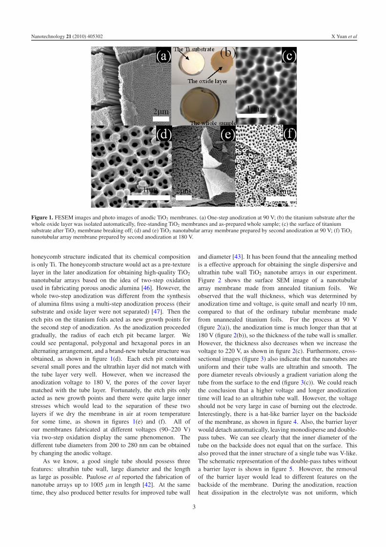
Figure 1(a) shows the SEM image of TiO2 nanotubular arraysthrough the one-step oxidation. However, there is a thinlayer with irregular holes on the tubular structure and theTiO2 nanotubes are not dispersed, while it is noticed thatthe whole oxide layer can be isolated from the titanium foilsautomatically when the anodization time is about 4 h afterdrying in air for some time, as shown in figure 1(b). Next weobserved the backside of the oxide layer. Unfortunately, in thisone-step oxidation, the barrier layers with a thickness of about0.5 µm were not separated from the tube layers completely.
In particular, it was observed that the surface of titaniumfoil without an oxide layer has a honeycomb structure(each cell is actually an etch pit, as shown in figure 1(c)).Furthermore, EDX spectroscopy of the surface of the
2
Nanotechnology 21 (2010) 405302 X Yuan et al
Figure 1. FESEM images and photo images of anodic TiO2 membranes. (a) One-step anodization at 90 V; (b) the titanium substrate after thewhole oxide layer was isolated automatically, free-standing TiO2 membranes and as-prepared whole sample; (c) the surface of titaniumsubstrate after TiO2 membrane breaking off; (d) and (e) TiO2 nanotubular array membrane prepared by second anodization at 90 V; (f) TiO2
nanotubular array membrane prepared by second anodization at 180 V.
honeycomb structure indicated that its chemical compositionis only Ti. The honeycomb structure would act as a pre-texturelayer in the later anodization for obtaining high-quality TiO2
nanotubular arrays based on the idea of two-step oxidationused in fabricating porous anodic alumina [46]. However, thewhole two-step anodization was different from the synthesisof alumina films using a multi-step anodization process (theirsubstrate and oxide layer were not separated) [47]. Then theetch pits on the titanium foils acted as new growth points forthe second step of anodization. As the anodization proceededgradually, the radius of each etch pit became larger. Wecould see pentagonal, polygonal and hexagonal pores in analternating arrangement, and a brand-new tubular structure wasobtained, as shown in figure 1(d). Each etch pit containedseveral small pores and the ultrathin layer did not match withthe tube layer very well. However, when we increased theanodization voltage to 180 V, the pores of the cover layermatched with the tube layer. Fortunately, the etch pits onlyacted as new growth points and there were quite large innerstresses which would lead to the separation of these twolayers if we dry the membrane in air at room temperaturefor some time, as shown in figures 1(e) and (f). All ofour membranes fabricated at different voltages (90–220 V)via two-step oxidation display the same phenomenon. Thedifferent tube diameters from 200 to 280 nm can be obtainedby changing the anodic voltage.
As we know, a good single tube should possess threefeatures: ultrathin tube wall, large diameter and the lengthas large as possible. Paulose et al reported the fabrication ofnanotube arrays up to 1005 µm in length [42]. At the sametime, they also produced better results for improved tube wall
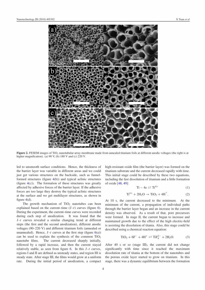
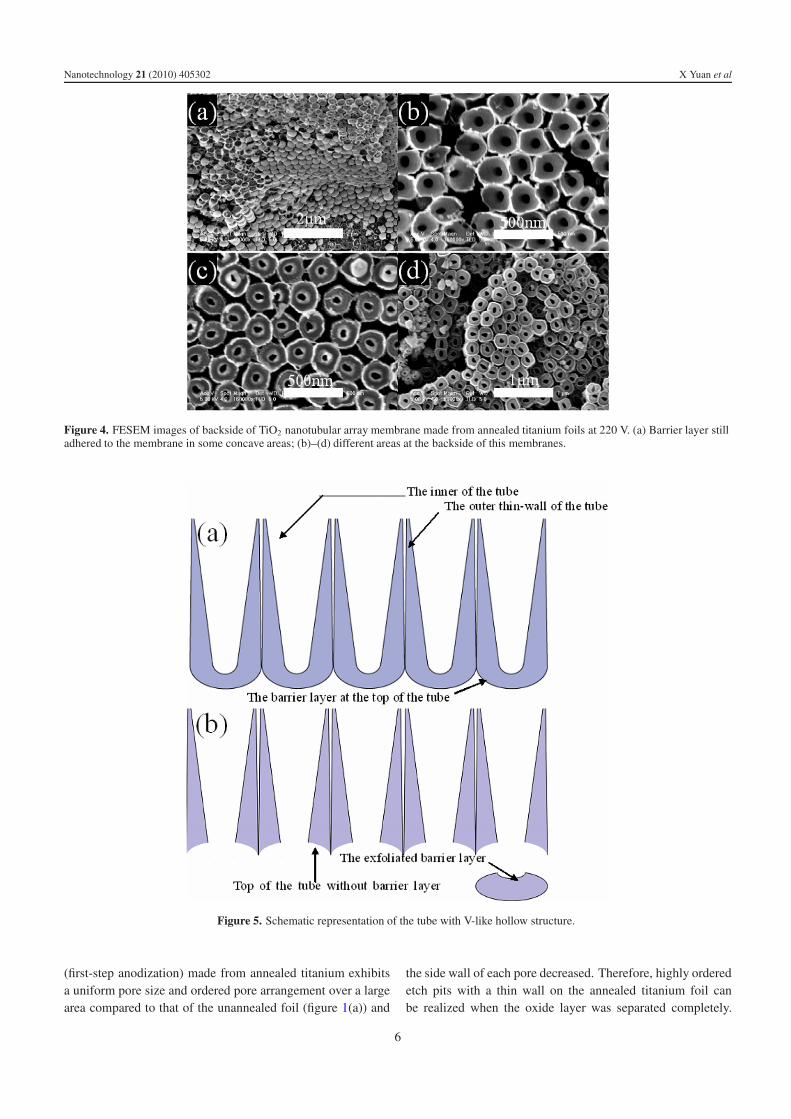
and diameter [43]. It has been found that the annealing methodis a effective approach for obtaining the single dispersive andultrathin tube wall TiO2 nanotube arrays in our experiment.Figure 2 shows the surface SEM image of a nanotubulararray membrane made from annealed titanium foils. Weobserved that the wall thickness, which was determined byanodization time and voltage, is quite small and nearly 10 nm,compared to that of the ordinary tubular membrane madefrom unannealed titanium foils. For the process at 90 V(figure 2(a)), the anodization time is much longer than that at180 V (figure 2(b)), so the thickness of the tube wall is smaller.However, the thickness also decreases when we increase thevoltage to 220 V, as shown in figure 2(c). Furthermore, cross-sectional images (figure 3) also indicate that the nanotubes areuniform and their tube walls are ultrathin and smooth. Thepore diameter reveals obviously a gradient variation along thetube from the surface to the end (figure 3(c)). We could reachthe conclusion that a higher voltage and longer anodizationtime will lead to an ultrathin tube wall. However, the voltageshould not be very large in case of burning out the electrode.Interestingly, there is a hat-like barrier layer on the backsideof the membrane, as shown in figure 4. Also, the barrier layerwould detach automatically, leaving monodisperse and double-pass tubes. We can see clearly that the inner diameter of thetube on the backside does not equal that on the surface. Thisalso proved that the inner structure of a single tube was V-like.The schematic representation of the double-pass tubes withouta barrier layer is shown in figure 5. However, the removalof the barrier layer would lead to different features on thebackside of the membrane. During the anodization, reactionheat dissipation in the electrolyte was not uniform, which
3
Nanotechnology 21 (2010) 405302 X Yuan et al
Figure 2. FESEM images of TiO2 nanotubular array membrane made from annealed titanium foils at different anodic voltages (the right is athigher magnification). (a) 90 V, (b) 180 V and (c) 220 V.
led to unsmooth surface conditions. Hence, the thickness ofthe barrier layer was variable in different areas and we couldjust get various structures on the backside, such as funnel-formed structures (figure 4(b)) and typical aclinic structures(figure 4(c)). The formation of these structures was greatlyaffected by adhesive forces of the barrier layer. If the adhesiveforces are too large they destroy the typical aclinic structuresat the surface and we get multilayer structures, as shown infigure 4(d).
The growth mechanism of TiO2 nanotubes can beenexplained based on the current–time (I –t) curves (figure 6).During the experiment, the current–time curves were recordedduring each step of anodization. It was found that theI –t curves revealed a similar changing trend at differentsteps (the first and the second anodization), different anodicvoltages (90–220 V) and different titanium foils (annealed orunannealed). Hence, I –t curves at the first step (figure 6(a))can be used to explain the synthesis of the common TiO2
nanotube films. The current decreased sharply initially,followed by a rapid increase, and then the current stayedrelatively stable, as seen from figure 6. In this I –t curves,regions I and II are defined as unsteady states, and region III issteady state. After stage III, the films would grow at a uniformrate. During the initial period of anodization, a compact
high-resistant oxide film (the barrier layer) was formed on thetitanium substrate and the current decreased rapidly with time.This initial stage could be described by these two equations,including the fast dissolution of titanium and a little formationof oxide [48, 49]:
Ti − 4e � Ti4+ (1)
Ti4+ + 2H2O → TiO2 + 4H+. (2)
At 10 s, the current decreased to the minimum. At theminimum of the current, a propagation of individual pathsthrough the barrier layer began and an increase in the currentdensity was observed. As a result of that, pore precursorswere formed. In stage II, the current began to increase andmaintained growth due to the effect of the high electric-fieldis assisting the dissolution of titania. Also, this stage could bedescribed using a chemical reaction equation:
TiO2 + 6F− + 4H+ � TiF2−6 + 2H2O. (3)
After 40 s or so (stage III), the current did not changesignificantly with time since it reached the maximumdissolution rate of titania at the bottom of the nanotubes andthe porous oxide layer started to grow on titanium. In thisstage, there was a dynamic equilibrium between the formation
4
Nanotechnology 21 (2010) 405302 X Yuan et al
Figure 3. Cross-sectional FESEM images of TiO2 nanotubular array membrane made from annealed titanium foils at different voltages:(a) 90 V; (b) 180 V; (c) 220 V; (d) the whole cross-sectional image of the film at 180 V; (e) surface FESEM images of TiO2 nanotubular arraymembrane made from annealed titanium foils at the first step of anodization; (f) the higher magnification of (e).
and dissolution of titania, that is the growth rate of the oxidelayer equals that of oxide dissolution. But the barrier layerstill adheres to the oxide layer and moves deeper into the metalwithout any change and made the pore also deeper at the sametime. A higher-field anodization will lead to a much thickeroxide layer. Interestingly, these processes were quite similar tothose of alumina [50, 51].
As the time of the unsteady states is too short (10 s)compared to the steady state (20 min or more), we only usethe time of the steady state as the growth time. The growthrate (R) can be calculated using the formula R = h/t . Hereh means the thickness of the film, which could be measuredfrom SEM morphology (figure 3(d)), and t is the growth time.The growth rates at each voltage were shown in table 1. In ourexperiments, growth rate of the membranes varied from 0.40to 1.00 µm min−1 when the anodization voltages varied from
90 to 220 V. The growth rate in our experiments has improvedgreatly and nearly 16 times as much as in traditional fabrication(0.0625 µm min−1, 360 µm for 96 h) of TiO2 at low field [42].
The formation of a V-like structure with ultrathin tube wallTiO2 nanotube arrays by using annealed titanium foils shouldbe due to the change in microstructure of the foil. We examinedtwo titanium foils by x-ray diffraction, shown in figure 7. Thepeak intensity of the annealed titanium is a bit weaker than thatof the unannealed one and there is very little amount of rutileTiO2 mixed with Ti. Hence, the granulation process occursin the whole titanium foils during the annealing, and titaniumatoms could be activated due to high surface area, which willbe beneficial to the fast dissolution of titanium (reaction (1)).This will result in the generation of a larger current duringanodization, which will lead to the formation of high-qualityordered pore films [46]. Figures 3(e) and (f) show that the film
5
Nanotechnology 21 (2010) 405302 X Yuan et al
Figure 4. FESEM images of backside of TiO2 nanotubular array membrane made from annealed titanium foils at 220 V. (a) Barrier layer stilladhered to the membrane in some concave areas; (b)–(d) different areas at the backside of this membranes.
Figure 5. Schematic representation of the tube with V-like hollow structure.
(first-step anodization) made from annealed titanium exhibitsa uniform pore size and ordered pore arrangement over a largearea compared to that of the unannealed foil (figure 1(a)) and
the side wall of each pore decreased. Therefore, highly orderedetch pits with a thin wall on the annealed titanium foil canbe realized when the oxide layer was separated completely.
6
Nanotechnology 21 (2010) 405302 X Yuan et al
(a) (b)
Figure 6. (a) Variation of etching current with time at different voltages at the first stage. Regions I and II are defined as unsteady states andregion III is steady state; (b) variation of etching current with time at the same voltage (220 V) at the second stage for different titanium foils(curve A: unannealed titanium foils, curve B: annealed titanium foils).
Figure 7. X-ray diffraction patterns of the two different titaniumfoils. A is annealed titanium foil and B is unannealed titanium foil.R and T represent rutile and titanium, respectively.
Hence, this titanium foil will be beneficial in fabricating theTiO2 nanotubular layer with ultrathin tube walls during thesecond step. On the other hand, the current–time (I –t) curves(figure 6(b), recorded for the second step) also show that thecurrent is larger when we used annealed titanium foils thanfor unannealed ones at the same voltage. This indicates thatthe dissolution rate of annealed foils is also larger than thatof unannealed ones in the second-step anodization. Generally,a high field will lead to non-uniform distribution of hydrogenions (reaction (2)) in each tube and these gradient-distributedelectrolytes result in the formation of gradient pore diameter.Then the V-like tube forms gradually. Interestingly, the V-like structure could be formed, no matter whether the foil isannealed or unannealed. However, the V-like structure withultrathin tube walls is not obvious enough due to its loweranodization current when the unannealed foil was used. Hence,a large current is important for fabricating this V-like structurelayer with ultrathin tube walls, and a annealing process oftitanium is necessary.
An annealing process of the TiO2 membranes was furthercarried out for changing the morphologies and microstructures
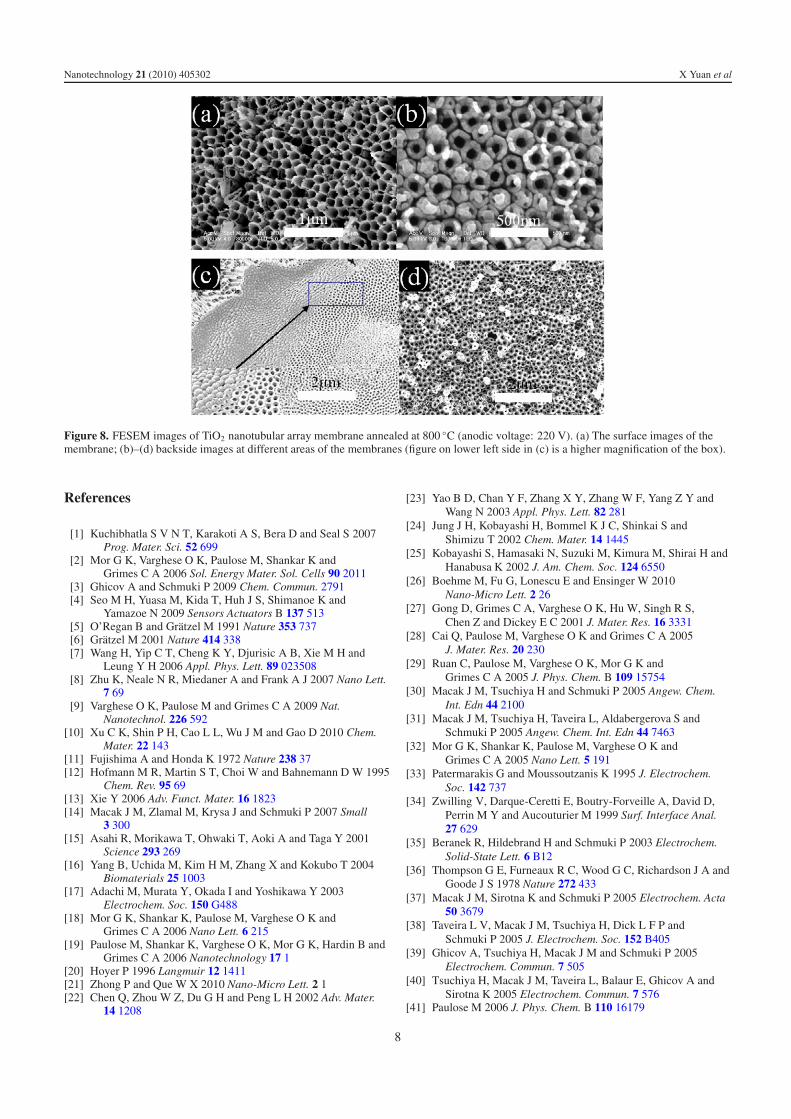
of the TiO2 membranes. The results indicate that at thehigher annealing temperature (above 800 ◦C) the structure ofthe tubes will be destroyed. Figure 8 shows the SEM upper sideand backside images of the annealed TiO2 nanotubular arraymembrane anodized at 220 V. It is noted that part of the barrierlayer can break off from the TiO2 membrane after annealingand the double-pass tube structures can be obtained, as shownin figures 8(a) and (d). However, membranes fabricatedat a lower anodization voltage (90 V) would not producedouble-pass tube structures after annealing. This indicates thatthe change in internal stress in the TiO2 nanotubular arraymembrane during annealing at a certain high temperature is thecrucial point for the formation of double-pass tube structures.This implies that an annealing process of the TiO2 nanotubulararray membranes fabricated by high-field anodization is alsoan effective approach to remove the barrier layer and obtaindouble-pass TiO2 nanotubes.
4. Conclusion
We have prepared highly ordered TiO2 porous membranes bytwo-step electrochemical oxidation under a stable high field,and the growth rate has improved greatly. A large currentis important for fabricating this V-like structure layer withultrathin tube walls. An annealing process will promote thebarrier layer removal from the surface of the TiO2 nanotubearray membranes automatically, and monodisperse tubes witha double-pass structure can be fabricated. This work providesan approach to improve the morphologies and microstructuresof TiO2 nanotube arrays.
Acknowledgments
This work was supported by the Natural Science Foundationof China (grant no. 10874115), the National MajorBasic Research Project of 2010CB933702, the ShanghaiNanotechnology Research Project of 0952nm01900, theShanghai Key Basic Research Project of 08JC1411000 and theResearch fund for the Doctoral Program of Higher Educationof China.
7
Nanotechnology 21 (2010) 405302 X Yuan et al
Figure 8. FESEM images of TiO2 nanotubular array membrane annealed at 800 ◦C (anodic voltage: 220 V). (a) The surface images of themembrane; (b)–(d) backside images at different areas of the membranes (figure on lower left side in (c) is a higher magnification of the box).
References
[1] Kuchibhatla S V N T, Karakoti A S, Bera D and Seal S 2007Prog. Mater. Sci. 52 699
[2] Mor G K, Varghese O K, Paulose M, Shankar K andGrimes C A 2006 Sol. Energy Mater. Sol. Cells 90 2011
[3] Ghicov A and Schmuki P 2009 Chem. Commun. 2791[4] Seo M H, Yuasa M, Kida T, Huh J S, Shimanoe K and
Yamazoe N 2009 Sensors Actuators B 137 513[5] O’Regan B and Gratzel M 1991 Nature 353 737[6] Gratzel M 2001 Nature 414 338[7] Wang H, Yip C T, Cheng K Y, Djurisic A B, Xie M H and
Leung Y H 2006 Appl. Phys. Lett. 89 023508[8] Zhu K, Neale N R, Miedaner A and Frank A J 2007 Nano Lett.
7 69[9] Varghese O K, Paulose M and Grimes C A 2009 Nat.
Nanotechnol. 226 592[10] Xu C K, Shin P H, Cao L L, Wu J M and Gao D 2010 Chem.
Mater. 22 143[11] Fujishima A and Honda K 1972 Nature 238 37[12] Hofmann M R, Martin S T, Choi W and Bahnemann D W 1995
Chem. Rev. 95 69[13] Xie Y 2006 Adv. Funct. Mater. 16 1823[14] Macak J M, Zlamal M, Krysa J and Schmuki P 2007 Small
3 300[15] Asahi R, Morikawa T, Ohwaki T, Aoki A and Taga Y 2001
Science 293 269[16] Yang B, Uchida M, Kim H M, Zhang X and Kokubo T 2004
Biomaterials 25 1003[17] Adachi M, Murata Y, Okada I and Yoshikawa Y 2003
Electrochem. Soc. 150 G488[18] Mor G K, Shankar K, Paulose M, Varghese O K and
Grimes C A 2006 Nano Lett. 6 215[19] Paulose M, Shankar K, Varghese O K, Mor G K, Hardin B and
Grimes C A 2006 Nanotechnology 17 1[20] Hoyer P 1996 Langmuir 12 1411[21] Zhong P and Que W X 2010 Nano-Micro Lett. 2 1[22] Chen Q, Zhou W Z, Du G H and Peng L H 2002 Adv. Mater.
14 1208
[23] Yao B D, Chan Y F, Zhang X Y, Zhang W F, Yang Z Y andWang N 2003 Appl. Phys. Lett. 82 281
[24] Jung J H, Kobayashi H, Bommel K J C, Shinkai S andShimizu T 2002 Chem. Mater. 14 1445
[25] Kobayashi S, Hamasaki N, Suzuki M, Kimura M, Shirai H andHanabusa K 2002 J. Am. Chem. Soc. 124 6550
[26] Boehme M, Fu G, Lonescu E and Ensinger W 2010Nano-Micro Lett. 2 26
[27] Gong D, Grimes C A, Varghese O K, Hu W, Singh R S,Chen Z and Dickey E C 2001 J. Mater. Res. 16 3331
[28] Cai Q, Paulose M, Varghese O K and Grimes C A 2005J. Mater. Res. 20 230
[29] Ruan C, Paulose M, Varghese O K, Mor G K andGrimes C A 2005 J. Phys. Chem. B 109 15754
[30] Macak J M, Tsuchiya H and Schmuki P 2005 Angew. Chem.Int. Edn 44 2100
[31] Macak J M, Tsuchiya H, Taveira L, Aldabergerova S andSchmuki P 2005 Angew. Chem. Int. Edn 44 7463
[32] Mor G K, Shankar K, Paulose M, Varghese O K andGrimes C A 2005 Nano Lett. 5 191
[33] Patermarakis G and Moussoutzanis K 1995 J. Electrochem.Soc. 142 737
[34] Zwilling V, Darque-Ceretti E, Boutry-Forveille A, David D,Perrin M Y and Aucouturier M 1999 Surf. Interface Anal.27 629
[35] Beranek R, Hildebrand H and Schmuki P 2003 Electrochem.Solid-State Lett. 6 B12
[36] Thompson G E, Furneaux R C, Wood G C, Richardson J A andGoode J S 1978 Nature 272 433
[37] Macak J M, Sirotna K and Schmuki P 2005 Electrochem. Acta50 3679
[38] Taveira L V, Macak J M, Tsuchiya H, Dick L F P andSchmuki P 2005 J. Electrochem. Soc. 152 B405
[39] Ghicov A, Tsuchiya H, Macak J M and Schmuki P 2005Electrochem. Commun. 7 505
[40] Tsuchiya H, Macak J M, Taveira L, Balaur E, Ghicov A andSirotna K 2005 Electrochem. Commun. 7 576


![Heterostructured ZnFe2O4/Fe2TiO5/TiO2 Composite Nanotube … · 2017-11-17 · hydrogen production via water splitting [8–10], photocat-alytic degradation of organic pollutants](https://static.documents.pub/doc/80x56/5e680e512e67a35e30098bf0/heterostructured-znfe2o4fe2tio5tio2-composite-nanotube-2017-11-17-hydrogen-production.jpg)


![Effect of Tantalum Doping on TiO2 Nanotube Arrays …A. Pozio 2 thium batteries [18] and also in different biological and medical reasearches, like the osteoblast growth [19]-[22]](https://static.documents.pub/doc/80x56/5f13a567587f4a74b061b363/effect-of-tantalum-doping-on-tio2-nanotube-arrays-a-pozio-2-thium-batteries-18.jpg)


