The ATLAS L1Calo collaborationArgonne, Birmingham, Cambridge, Heidelberg,
Mainz, MSU, QMUL, RAL, Stockholm
Uli Schäfer 14.02.2011 08:39:32
2
Outline
• Current Level-1 Calorimeter Trigger• Latency…• Upgrade for higher luminosity: Phase 1• Towards Phase 2• Mainz R&D activities
Uli Schäfer
3
ATLAS Trigger / current L1Calo
Uli Schäfer
Jet/Energy module
caloµ
CTP
L1
4
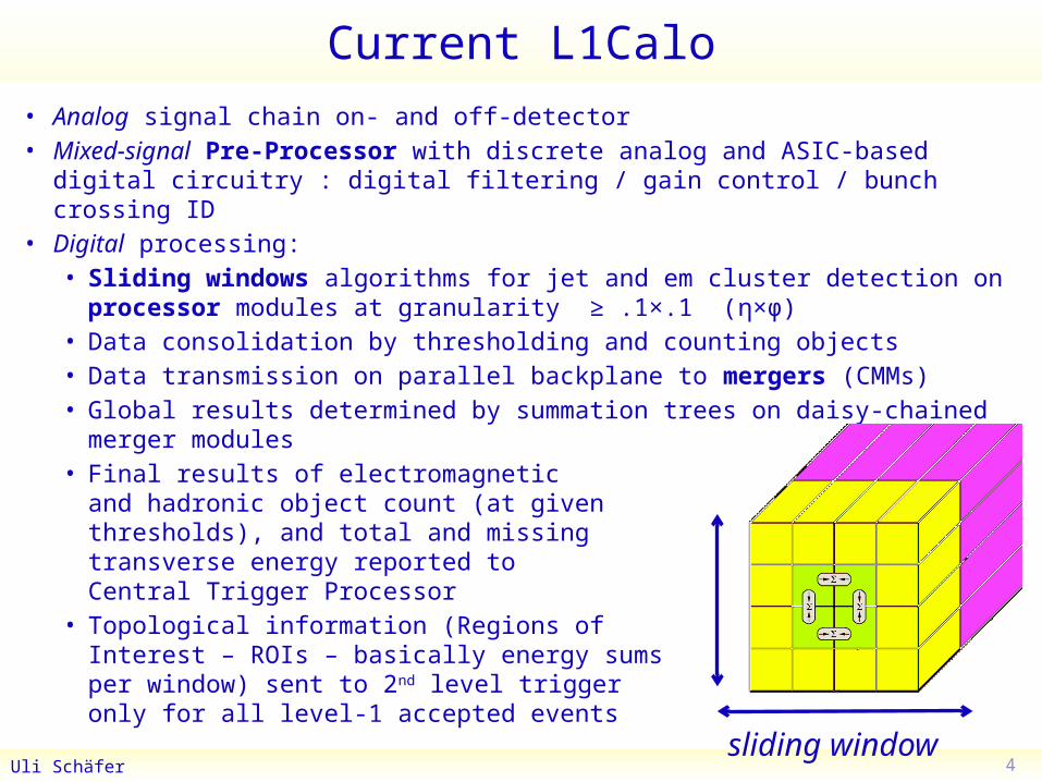
Current L1Calo• Analog signal chain on- and off-detector • Mixed-signal Pre-Processor with discrete analog and ASIC-based
digital circuitry : digital filtering / gain control / bunch crossing ID• Digital processing:
• Sliding windows algorithms for jet and em cluster detection on processor modules at granularity ≥ .1×.1 (η×φ)
• Data consolidation by thresholding and counting objects• Data transmission on parallel backplane to mergers (CMMs)• Global results determined by summation trees on daisy-chained
merger modules• Final results of electromagnetic
and hadronic object count (at given thresholds), and total and missing transverse energy reported to Central Trigger Processor
• Topological information (Regions of Interest – ROIs – basically energy sumsper window) sent to 2nd level triggeronly for all level-1 accepted events
Uli Schäfersliding window
5
Latency, algorithms, data paths …
Total latency limited to c. 2.5 microseconds (cables!)Sliding windows algorithms require duplication of data across processor module and crate boundaries All real-time data transmitted electrically• Analogue off the detector• 480 Mb/s differential into digital processors, data
replication at source• 80 / 160 Mb/s single ended data replicated over a custom
backplane• 40 Mb/s to, between & from merger modules (CMMs)
System works well, latency limits met. Complicated and expensive processor backplane (18 layers) and considerable cable plant
Uli Schäfer
6
The horror lurks behind…
Uli Schäfer
Jet/Energyprocessor
Pre-processor
Jet/En. processor
7
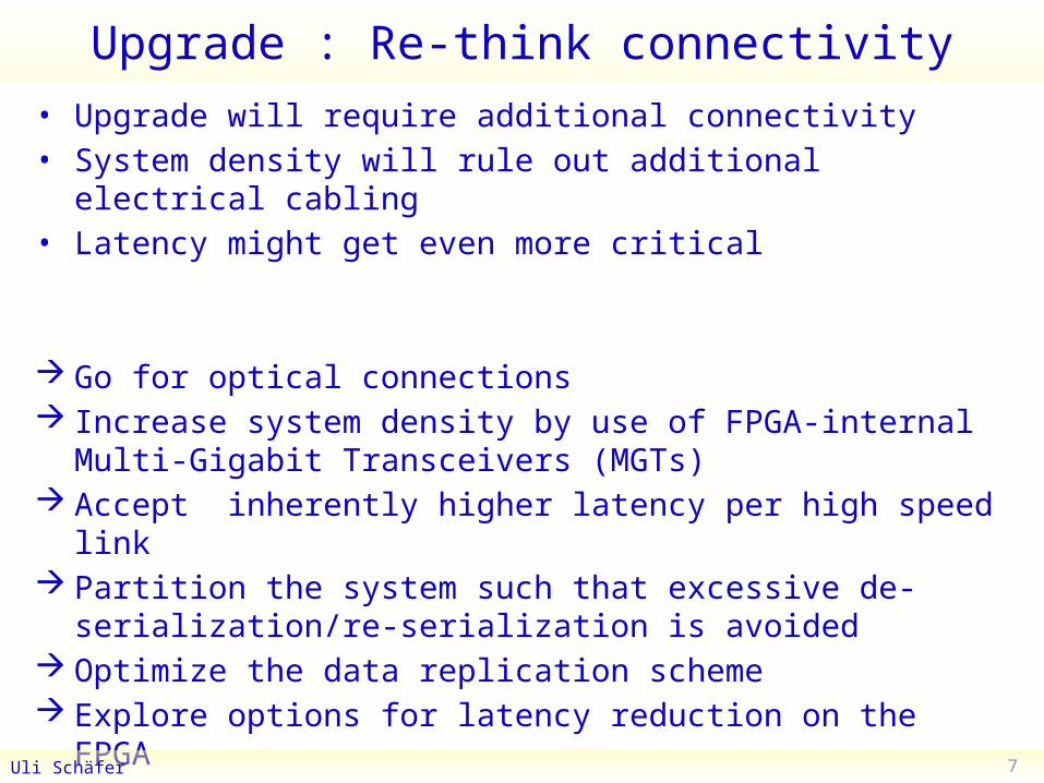
Upgrade : Re-think connectivity• Upgrade will require additional connectivity• System density will rule out additional electrical cabling• Latency might get even more critical
Go for optical connections Increase system density by use of FPGA-internal Multi-
Gigabit Transceivers (MGTs) Accept inherently higher latency per high speed link Partition the system such that excessive
de-serialization/re-serialization is avoided Optimize the data replication scheme Explore options for latency reduction on the FPGA
Uli Schäfer
8
Data replication
Forward data replication only:• Duplication at source
• Mirror a link• Assemble a different stream optimised for the
replication• Optical splitter (fibre coupler)
Uli Schäfer
Do not share any data between modules of same subsystem to avoid additional SerDes latency
source
sink
9
L1Calo upgrade stepsDue to expected increase in pile-up of events at rising luminosities, the current algorithms will be degraded. Improve L1Calo in distinct phases• Phase 0 :
• Some improvements on the FPGA based algorithms have been made and will be in use for 2011 running
• Further optimizations might follow• No hardware being added / replaced at this stage
• Phase 1 :• Improve digital signal processing on Pre-Processor ( ASIC FPGA )• Add topological processing with limited hardware changes
• Phase-2 : • Improve of granularity of L1Calo algorithms in η, φ, and depth • Replace Level-1 Calorimeter Trigger• Probably distinguish Level-0 and Level-1 trigger
NB :1. This is a snapshot of current thinking only. Level-1 technical proposal being written2. Stages are related to, but not strictly dependent on the LHC machine upgrade steps3. L1Calo will attempt to stage the installation of new hardware (sub-phases)4. Phase-1 is mainly internal to L1Calo, no strict need for mods of external interfaces5. Phase-2 is dependent on calorimeter readout electronics upgrade
Uli Schäfer
10
Phase 1: Topology• So far topology of identified objects not propagated through
1st level trigger real-time data path for bandwidth reason Increase RTDP bandwidth and send (almost) full ROI information to a
single processor stage where topology cuts are applied and double counting is suppressed by jet/electron/... matching :
• Increase backplane bandwidth of existent processor modules 4-fold (40Mb/s160Mb/s) with modification to FPGA code only
• Replace the CMM merger modules by “CMM++” modules• Single FPGA processor• 64Gb/s backplane input capability • Possibly up to ~400Gb/s optical I/O
• Star-couple all CMM++s into topological processor • Include Muon processing capability on topological processor
• Backward compatible to current scheme (for staged installation) : CMM++ daisy-chain (electrical / optical)
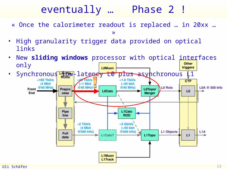
« Once the calorimeter readout is replaced … in 20xx … »• High granularity trigger data provided on optical links• New sliding windows processor with optical interfaces only• Synchronous low-latency L0 plus asynchronous L1
14
Upgrade activities in Mainz• Simulations of topological algorithms at high luminosities
(1034 cm-2s-1), high pile-up• Simulation and implementation of the algorithms in VHDL• Improvements on VHDL code for current processors• Design of demonstrator modules for phase 1 and phase 2
• Topological processor• Phase-2 Level-0 sliding windows processor
• Latency optimization • Data replication schemes • FPGA on-chip MGT operation modes and fabric
interfaces
Uli Schäfer
15
Demonstrators / Prototypes so far…
• Work on a CMM++ prototype has started recently at MSU. Currently at specifications stage. Will serve as data input for the topological processor
• “GOLD” demonstrator (not just) for a topological processor currently being developed in Mainz Latency data replication schemesDensity processing power, connectivityUli Schäfer
• Mainz-built “BLT” backplane and link tester, equipped with Avago opto-link interface (12-channel, 6.4Gb/s) and LHC bunch clock jitter cleaning hardware.Successfully verified backplane data reception (160Mb/s) and opto link operation.
16
GOLD – Generic Opto Link Demonstrator
«data concentrator» scheme:
many in – few out• Advanced TCA form factor• Limited connectivity on
front panel• Input links via optical
connectors in zone 3• 12-channel 10Gb/s opto
modules on daughter card
• Electrical connectivity up to 10Gb/s in zone 2
• Power budget ~400W
Uli Schäfer
RTMfront
ATCA
Z2
Z3back
17
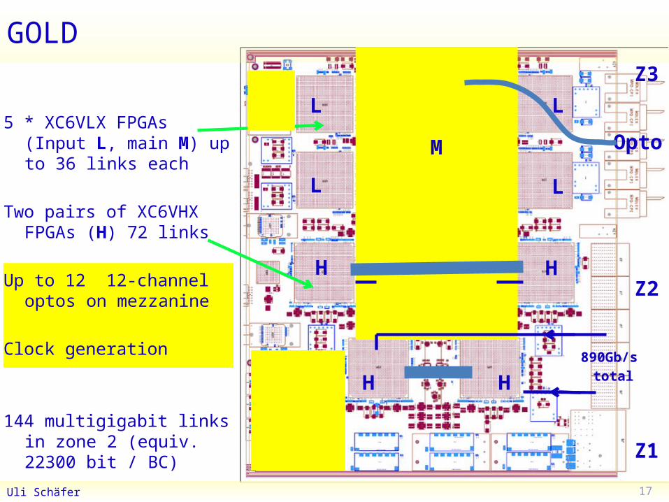
GOLD
Uli Schäfer
Z1
Z2
Z3
Opto
L
L L
L
H H
H H
5 * XC6VLX FPGAs(Input L, main M) up to 36 links each
Two pairs of XC6VHX FPGAs (H) 72 links
Up to 12 12-channel optos on mezzanine
Clock generation
144 multigigabit links in zone 2 (equiv. 22300 bit / BC)
M
890Gb/s total
18
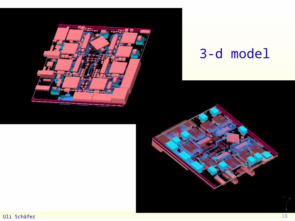
3-d model
Uli Schäfer
19
Module status
Uli Schäfer
• Main board finished• Carefully hand-
routed (~ 400 differential pairs per FPGA, line rates 1.0/6.5/10 Gbps)
• Daughter modules almost done
• Will have several incarnations of daughter modules
• L1Calo-internal review soon
• Components available …
20
Components…
Uli Schäfer
opto mezzanine
data replication atCML level
12 to 72 fibres per backplane connector (MPO/MTP)
10Gb/s Opto
clock mezzanine
21
Current activities: h/w, f/w• Main focus on GOLD hardware design / production• First module tests spring 2011, further hardware
development for phase1 Topo-processor and phase2 (Virtex-7, up to 28Gb/s)
• Characterize 6.5/10Gbps optical link chipsets (Avago)• Work on latency minimization for Xilinx MGTs operated
synchronous to LHC bunch clock, with phase alignment
Uli Schäfer
GTX receiverReceived clock | LHC clock
22
Some current activities• Default encoding (for phase 1 topo) 8b/10b,
80% payload• Successfully tested a variant for latency critical paths:
• Transmit raw data, alternating normal and inverted representation
• 50% payload, latency reduction by c. 1 LHC bunch tick• Suppression of elastic buffer
• Works out of the box with Xilinx IP core for small channel count
• Fails for large channel count due to insufficient global routing resources
• Will probably require to devise specific scheme for re-synchronisation to global LHC bunch clock
Uli Schäfer
23
Summary / outlook• Need for substantial improvement of trigger algorithms• Topological processor (phase-1) and new sliding windows