58 IEEE JOURNAL OF SELECTED TOPICS IN QUANTUM ELECTRONICS, VOL. 13, NO. 1, JANUARY/FEBRUARY 2007
High-Speed OTDM and WDM Networks UsingTraveling-Wave Electroabsorption Modulators
Hsu-Feng Chou, Member, IEEE, and John E. Bowers, Fellow, IEEE
(Invited Paper)
Abstract—We describe the design and performance of a numberof elements based on traveling-wave electroabsorption modulators(TW-EAMs) in optical time-division-multiplexing (OTDM) andwavelength-division-multiplexing (WDM) networks. The incorpo-ration of traveling-wave (TW) electrode design into electroabsorp-tion modulators (EAMs) relieves the resistance–capacitance (RC)bandwidth limitation common to lumped components, enablinghigher operation speed without shortening the device. As a result,high-speed operation can be combined with essential modulatorcharacteristics such as modulation efficiency and extinction ra-tio. While significant modulation bandwidth has been achieved, alesser known aspect is that the TW electrode also provides an ex-tra dimension for improving and enabling functionalities beyondbroadband modulation. This new dimension originates from thedistributed effect of the TW design and its interactions with dis-tinctive EAM properties. This paper reviews such developmentsin recent years with specific applications for optical signal pro-cessing in OTDM and WDM networks. The covered functionalitiesinclude various optical gating operations for OTDM, regenerativewavelength conversions for WDM, and clock recovery.
OVER the past few decades, fiber-optic communicationshave made significant progress in providing higher trans-
mission capacity with lower cost. The success of the Internet,which already changed human society globally, benefited fromthe developments in fiber-optics technology. Given the ∼100%per year growth observed in the past few years [1], Internettraffic is expected to increase by a thousand times in the nextten years, which poses a severe challenge to the present opticalnetwork. To scale for future traffic, the optical network needs tohandle higher data rates and larger capacity while offering moreflexibility. The most promising solution is an optical networkthat utilizes optical signal processing in the time, wavelength,and space domains. The specific technologies involved are,respectively, optical time-division multiplexing (OTDM) [2],wavelength, division multiplexing (WDM) [3], and large-scale
Manuscript received August 3, 2006; revised September 21, 2006. This workwas supported by the Defense Advanced Research Projects Agency (DARPA)CS-WDM program.
H.-F. Chou was with the Department of Electrical and Computer Engineering,University of California, Santa Barbara, CA 93106 USA. He is now with Lumi-nentOIC Inc., Chatsworth, CA 91311 USA (e-mail: [email protected]).
J. E. Bowers is with the Department of Electrical and Computer Engineer-ing, University of California, Santa Barbara, CA 93106 USA (e-mail: [email protected]).
Digital Object Identifier 10.1109/JSTQE.2006.887152
photonic cross connects (PXC) [4]. Even though impressivetransmission speed and capacity has been demonstrated usingOTDM [5] and WDM [6], many challenges remain ahead forboth technologies. For OTDM, it is crucial to develop compactcomponents and subsystems with reduced complexity for prac-tical deployment. On the other hand, the flexibility of WDMnetworks would be greatly improved if efficient and compactregenerative wavelength converters are available. This paperreviews the design and application of traveling-wave electroab-sorption modulators (TW-EAMs) that can provide novel solu-tions in response to the demands of the future optical networks.
II. TW EAMS AND THEIR UNIQUE PROPERTIES
The electroabsorption modulator (EAM) is a compact, effi-cient, and integrable component for fiber-optic communications.It utilizes either the Franz–Keldysh effect in bulk material, orthe quantum-confined Stark effect in a multiple-quantum-well(MQW) structure to change the absorption of light accordingto the applied electric field [7]. MQW structures are widelyused for their higher modulation efficiency, but the wavelengthdependence is generally higher than for bulk material. The gen-eral advantages of EAMs over other types of modulators in-clude: 1) a small device dimension, usually on the order of afew hundred micrometers or less; 2) a lower driving voltagedue to its highly efficient and nonlinear electro-optical (E-O)transfer function; and 3) the possibility of monolithic integra-tion with other semiconductor components. EAMs with lumpedelectrodes have been demonstrated to exhibit a small-signal3-dB bandwidth over 40 GHz [8].
A critical design issue of the EAM is the tradeoff betweenthe modulation bandwidth and efficiency. The bandwidth ofa lumped-electrode EAM is determined by the resistance–capacitance (RC) time constant. To enable high-speed broad-band modulation, the active waveguide length (and width) mustbe short in order to keep the capacitance low. For example,in [8], a 40-Gb/s device is only 63 µm long and extra-passiveoptical waveguides are necessary to extend the device size foreasier handling. The main concern of a short active length isthe reduced modulation efficiency (expressed in dB/V), whichcan result in a higher driving voltage. In addition, the total ex-tinction ratio is reduced. For broadband modulation, 10 dB ofdynamic extinction ratio may be adequate, but for applicationslike optical gating in OTDM, very high extinction ratios arerequired. Another issue for a short device is the reduced opti-cal power handling capability, which is particularly critical forradio frequency (RF) photonic links.
CHOU AND BOWERS: HIGH-SPEED OTDM AND WDM NETWORKS USING TRAVELING-WAVE ELECTROABSORPTION MODULATORS 59
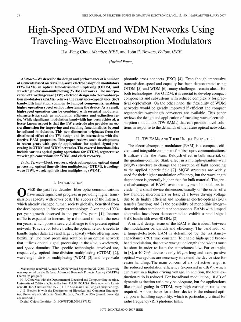
Fig. 1. Schematic diagram of a TW-EAM [13]. In our designs, the activewaveguide length can vary from 100 to 600 µm and the ground–signal–groundmicrowave coplanar waveguide feed lines are 500 µm long.
To overcome the tradeoff between bandwidth and devicelength, EAMs with traveling-wave (TW) electrodes were de-veloped [9]–[15], where the bandwidth is not limited by lumpedRC and the device length can be longer with a higher band-width. A typical implementation is illustrated schematically inFig. 1. In the TW design, the driving signal propagates throughthe active waveguide, which is in fact a microwave transmis-sion line. The junction capacitance of the EAM is no longermodeled as a lumped load but becomes distributed, particularlyat high frequencies. With a longer device length, the modu-lation efficiency can be kept high so that only a low drivingvoltage is required to reach a certain dynamic extinction ratio.For example, 30-dB/V peak modulation efficiency, 1-Vpp (Voltpeak-to-peak) driving voltage for error-free 10-Gb/s operation,and 14-dBm optical saturation power have been reported ona 300-µm-long InGaAsP-based TW-EAM [13]. Theoretically,the bandwidth and the useful device length of TW-EAM areonly limited by the microwave loss and the velocity mismatchbetween the lightwave and the microwave, and both determinehow long the lightwave can be effectively modulated by the mi-crowave driving signal [16], [17]. Another limiting factor is theincrease of optical scattering loss with device length, which candegrade the insertion loss of TW-EAM. Recently, an undercut-etching-active-region waveguide structure was reported to re-duce both the optical and the microwave losses by reducing thescattering loss and the cladding layer resistance [18].
A critical challenge for TW-EAM is a low characteristicimpedance of 25 Ω or below in the active waveguide, whichcauses reflections when driven by a 50-Ω source and limitsthe modulation bandwidth. The low impedance of the activewaveguide originates from the tradeoff between the junctioncapacitance with several critical device parameters such as op-tical and microwave losses as well as the driving voltage [16].Low impedance terminations in the range of 12 Ω to 35 Ω arerequired to optimize the bandwidth. For example, a bandwidthof 43 GHz was measured on a 450-µm-long device with a 13-Ωtermination [14]. One way to increase the device impedance isto use a segmented transmission line design to obtain a com-posite impedance of 50 Ω [19]. Flat response up to 50 GHz wasmeasured. Another practical solution is to use custom-made lowimpedance electronics to drive the TW-EAM. A recent devel-opment is a dual-depletion-region epilayer designed to reducethe junction capacitance, while keeping all the applied fielddrop across the MQW region to reduce driving voltage [20].The reduction of junction capacitance increases the character-
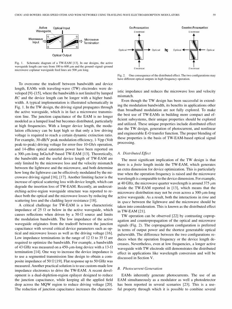
Fig. 2. One consequence of the distributed effect. The two configurations mayhave different optical outputs in high-frequency operation.
istic impedance and reduces the microwave loss and velocitymismatch.
Even though the TW design has been successful in extend-ing the modulation bandwidth, its benefits in applications otherthan broadband modulation are not fully explored. To makethe best use of TW-EAMs in building more compact and ef-ficient subsystems, their unique properties should be exploredand utilized. These unique properties include distributed effectdue the TW design, generation of photocurrent, and nonlinearand engineerable E-O transfer function. The proper blending ofthese properties is the basis of TW-EAM-based optical signalprocessing.
A. Distributed Effect
The most significant implication of the TW design is thatthere is a finite length inside the TW-EAM, which generatesan extra dimension for device optimization. This is particularlytrue when the operation frequency is raised and the microwavewavelength is comparable to the device dimension. For example,at 40 GHz, the microwave quarter wavelength is around 375 µminside the TW-EAM reported in [13], which means that themicrowave distribution may not be even across a 300-µm-longactive waveguide. As a result, both the interactions in time andin space between the lightwave and the microwave should betaken into consideration. This is known as the distributed effectin TW-EAM [21].
TW operation can be observed [22] by contrasting coprop-agation and counterpropagation of the optical and microwavesignals (Fig. 2). The copropagation configuration is preferredin terms of output power and the shortest generatable opticalpulsewidth. The difference between the two configurations re-duces when the operation frequency or the device length de-creases. Nevertheless, even at low frequencies, a longer activewaveguide with TW electrode still demonstrates the distributedeffect in applications like wavelength conversion and will bediscussed in Section V.
B. Photocurrent Generation
EAMs inherently generate photocurrents. The use of anEAM simultaneously as a modulator as well a photodetectorhas been reported in several scenarios [23]. This is a use-ful property through which it is possible to combine several
60 IEEE JOURNAL OF SELECTED TOPICS IN QUANTUM ELECTRONICS, VOL. 13, NO. 1, JANUARY/FEBRUARY 2007
Fig. 3. E-O transfer function of an EAM.
functionalities within a single TW-EAM. Note that for appli-cations in broadband modulation, a strong photocurrent insidethe active waveguide should be avoided, since it can lead to areduction of effective voltage supplied to the active region anddegrades the large signal dynamic extinction ratio, even beforethe active region is saturated by a high optical injection [24].
C. Nonlinear and Engineerable E-O Transformation
The E-O transfer function of an EAM is mainly determinedby the material design, and scaled by structural factors suchas device length, electrode design, and waveguide geometries.Many efforts have been focused on lowering the polarizationdependence by using strain-compensated MQW [10]. A typi-cal EAM E-O transfer function is shown in Fig. 3 on a linearscale, where three transmission regions can be identified: 1)high extinction (< 10%); 2) transition (10% to 90%); and 3) flattransmission (< 90%). In general, the transition voltage shouldbe small to achieve high modulation efficiency and low drivingvoltage. The slope of the transfer function varies point-to-pointdue to the nonlinear nature of electroabsorption. Nevertheless,it is possible to find certain points with minimized distortionfor high dynamic range RF photonic link [25]. Normally, thevoltage at which the transition begins (VH in Fig. 3) is designedclose to 0 V at the operating wavelength in order to reduceexcess heating. However, if VH can be shifted towards higherreverse voltage, more flat transmission region can be utilizedwithout forward biasing the TW-EAM, which is very useful forsignal reshaping [26].
III. GATING OPERATIONS IN OTDM NETWORKS
The most important form of optical signal processing inOTDM networks is optical gating. Specific functionalities in-clude optical pulse generation, demultiplexing, and add–dropmultiplexing. Numerous technologies based on fibers, semicon-ductor optical amplifiers (SOAs), and EAMs have been pro-posed and demonstrated. Brief reviews can be found in [2]. AnEAM is an ideal choice for optical gating, since even a sinu-soidal electrical driving signal is sufficient to generate a shortgating window due to the highly nonlinear E-O transfer func-tion of the EAM. This is a significant advantage in simplicityover all-optical gates, where an optical pulse source is requiredin addition to the gate itself. Other advantages include powerefficiency, small size, and the ability to monolithically integrate
Fig. 4. Schematic of microwave envelope in (a) traveling-wave mode; (b) and(c) standing-wave enhanced mode with different termination lengths.
with lasers, amplifiers, and photodetectors. However, to operateat high OTDM bit-rates of 160 Gb/s and beyond, the require-ments on gating window width and extinction ratio are stringentand the performance of electrically-driven EAM optical gatesneeds to be further improved.
There are four factors that determine the gating window shapeof an EAM: the modulation efficiency and the total extinctionratio of the device, and the waveform and the amplitude of thedriving signal. TW-EAMs can be longer than a lumped EAM andgain advantages in modulation efficiency and total extinctionratio. When a high base rate such as 40 Gb/s is adopted, theavailable electrical driving signal is most likely just a sinusoidalwave. Therefore, the remaining factor that can be improved isthe amplitude of the driving signal.
Since there is typically an impedance mismatch between thelow impedance of the TW-EAM and a 50-Ω source, the mi-crowave amplitude in the active waveguide can be smaller thandesired. One way to increase the microwave amplitude is to usetwo microwave amplifiers and drive the device from oppositeterminals [27]. For single-frequency operation, this is equivalentto forming a standing wave along the microwave transmissionline inside the TW-EAM, where the maximum swing can bedoubled in the ideal case. An alternative approach is to generatethe standing wave using an open termination instead of an extraamplifier, which is called the standing-wave enhanced mode ofTW-EAM [28].
As can be understood from Fig. 4, it is crucial to adjust thespatial phase of the standing wave so that the maximum swinghappens in the active waveguide. By fitting the measured re-sults with a theoretical model, it is found that getting an evenmicrowave distribution across the active waveguide is as impor-tant as increasing the maximum swing [28]. This indicates that athigh frequencies, the distributed effect is an important issue. On
CHOU AND BOWERS: HIGH-SPEED OTDM AND WDM NETWORKS USING TRAVELING-WAVE ELECTROABSORPTION MODULATORS 61
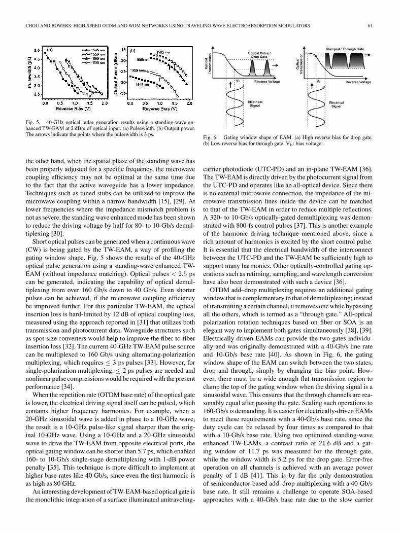
Fig. 5. 40-GHz optical pulse generation results using a standing-wave en-hanced TW-EAM at 2 dBm of optical input. (a) Pulsewidth. (b) Output power.The arrows indicate the points where the pulsewidth is 3 ps.
the other hand, when the spatial phase of the standing wave hasbeen properly adjusted for a specific frequency, the microwavecoupling efficiency may not be optimal at the same time dueto the fact that the active waveguide has a lower impedance.Techniques such as tuned stubs can be utilized to improve themicrowave coupling within a narrow bandwidth [15], [29]. Atlower frequencies where the impedance mismatch problem isnot as severe, the standing wave enhanced mode has been shownto reduce the driving voltage by half for 80- to 10-Gb/s demul-tiplexing [30].
Short optical pulses can be generated when a continuous wave(CW) is being gated by the TW-EAM, a way of profiling thegating window shape. Fig. 5 shows the results of the 40-GHzoptical pulse generation using a standing-wave enhanced TW-EAM (without impedance matching). Optical pulses < 2.5 pscan be generated, indicating the capability of optical demul-tiplexing from over 160 Gb/s down to 40 Gb/s. Even shorterpulses can be achieved, if the microwave coupling efficiencybe improved further. For this particular TW-EAM, the opticalinsertion loss is hard-limited by 12 dB of optical coupling loss,measured using the approach reported in [31] that utilizes bothtransmission and photocurrent data. Waveguide structures suchas spot-size converters would help to improve the fiber-to-fiberinsertion loss [32]. The current 40-GHz TW-EAM pulse sourcecan be multiplexed to 160 Gb/s using alternating-polarizationmultiplexing, which requires ≤ 3 ps pulses [33]. However, forsingle-polarization multiplexing, ≤ 2 ps pulses are needed andnonlinear pulse compressions would be required with the presentperformance [34].
When the repetition rate (OTDM base rate) of the optical gateis lower, the electrical driving signal itself can be pulsed, whichcontains higher frequency harmonics. For example, when a20-GHz sinusoidal wave is added in phase to a 10-GHz wave,the result is a 10-GHz pulse-like signal sharper than the orig-inal 10-GHz wave. Using a 10-GHz and a 20-GHz sinusoidalwave to drive the TW-EAM from opposite electrical ports, theoptical gating window can be shorter than 5.7 ps, which enabled160- to 10-Gb/s single-stage demultiplexing with 1-dB powerpenalty [35]. This technique is more difficult to implement athigher base rates like 40 Gb/s, since even the first harmonic isas high as 80 GHz.
An interesting development of TW-EAM-based optical gate isthe monolithic integration of a surface illuminated unitraveling-
Fig. 6. Gating window shape of EAM. (a) High reverse bias for drop gate.(b) Low reverse bias for through gate. Vb: bias voltage.
carrier photodiode (UTC-PD) and an in-plane TW-EAM [36].The TW-EAM is directly driven by the photocurrent signal fromthe UTC-PD and operates like an all-optical device. Since thereis no external microwave connection, the impedance of the mi-crowave transmission lines inside the device can be matchedto that of the TW-EAM in order to reduce multiple reflections.A 320- to 10-Gb/s optically-gated demultiplexing was demon-strated with 800-fs control pulses [37]. This is another exampleof the harmonic driving technique mentioned above, since arich amount of harmonics is excited by the short control pulse.It is essential that the electrical bandwidth of the interconnectbetween the UTC-PD and the TW-EAM be sufficiently high tosupport many harmonics. Other optically-controlled gating op-erations such as retiming, sampling, and wavelength conversionhave also been demonstrated with such a device [36].
OTDM add–drop multiplexing requires an additional gatingwindow that is complementary to that of demultiplexing; insteadof transmitting a certain channel, it removes one while bypassingall the others, which is termed as a “through gate.” All-opticalpolarization rotation techniques based on fiber or SOA is anelegant way to implement both gates simultaneously [38], [39].Electrically-driven EAMs can provide the two gates individu-ally and was originally demonstrated with a 40-Gb/s line rateand 10-Gb/s base rate [40]. As shown in Fig. 6, the gatingwindow shape of the EAM can switch between the two states,drop and through, simply by changing the bias point. How-ever, there must be a wide enough flat transmission region toclamp the top of the gating window when the driving signal is asinusoidal wave. This ensures that the through channels are rea-sonably equal after passing the gate. Scaling such operations to160-Gb/s is demanding. It is easier for electrically-driven EAMsto meet these requirements with a 40-Gb/s base rate, since theduty cycle can be relaxed by four times as compared to thatwith a 10-Gb/s base rate. Using two optimized standing-waveenhanced TW-EAMs, a contrast ratio of 21.6 dB and a gat-ing window of 11.7 ps was measured for the through gate,while the window width is 5.2 ps for the drop gate. Error-freeoperation on all channels is achieved with an average powerpenalty of 1 dB [41]. This is by far the only demonstrationof semiconductor-based add–drop multiplexing with a 40-Gb/sbase rate. It still remains a challenge to operate SOA-basedapproaches with a 40-Gb/s base rate due to the slow carrier
62 IEEE JOURNAL OF SELECTED TOPICS IN QUANTUM ELECTRONICS, VOL. 13, NO. 1, JANUARY/FEBRUARY 2007
Fig. 7. Concept of scaled OTDM clock recovery.
recovery dynamics. New developments in quantum-dot SOAmay provide possibilities of improved performance.
IV. CLOCK RECOVERY
In digital communication, clock recovery is essential to ac-quire synchronization at a network node or at the receiver end.Electronic phase-locked loop (PLL)-based clock recovery is amature and widely used technique to recover a low-jitter clock.However, there are two major challenges: 1) in an OTDM signal,the clock tone is at the line-rate frequency, which is inherentlyout of the reach of electronics and 2) the lock acquisition timemay not be fast enough for burst mode or packet signals, espe-cially at 40 Gb/s and above.
Many all-optical or optoelectronic techniques have been de-veloped in recent years to deal with these challenges. All-opticalinjection-locking techniques based on integrated semiconduc-tor devices are very attractive for their small dimension andhigh-speed potential [42], [43]. For instance, a mode-lockedlaser diode can be injection-locked by an optical 160-Gb/sreturn-to-zero (RZ) signal and generates 160-GHz optical clockpulses [42]. This type of clock recovery is ideal for high-speedall-optical amplitude, reshaping, and retiming (3-R) regener-ation at the line rate [44]. It is relatively difficult for theseall-optical injection-locked approaches to lock at the base rate,because subharmonic tones are either not present or very lowin an OTDM signal. Unfortunately, base-rate clocks are essen-tial for demultiplexing and add–drop multiplexing. Assistivetechniques can be used to improve the performance but at theexpense of increased complexity [45], [46].
In terms of subharmonic clock recovery, a more commonlyused approach is the combination of an optical demultiplexerand an electronic clock recovery that operates at the baserate [47], [48]. The concept of this scaled OTDM clock recoveryis depicted in Fig. 7. In this approach, the optical demultiplexerbrings the line-rate signal down to the base rate, at which theelectronic clock recovery is able to handle. However, the demul-tiplexer is driven by the clock recovered by the electronic clockrecovery. This extra feedback loop makes the locking acquisi-tion process more complicated than that of the original base-rateoperation. Assuming that the electronic clock recovery circuit isa standard PLL, a theoretical model can be developed to studythe phase-locking dynamics [49]. The results show that: 1) thereexists an optimal demultiplexing window width that optimizesthe lock-in range; 2) the optimal lock-in range is inversely pro-portional to the number of multiplexing; and 3) with an optimaldemultiplexing window width, the average lock-in time is in-dependent of the number of multiplexing, but dependent on theratio of frequency detuning to the lock-in range. In short, thebest possible performance can be achieved when the demulti-plexing window width is chosen properly. For example, if the
Fig. 8. Scaled simultaneous clock recovery and demultiplexing [53].
Fig. 9. TW-EAM ring oscillator clock recovery [54].
signal pulsewidth is 50% of the line-rate bit-slot, the optimaldemultiplxing window width is around 37%. To scale to a veryhigh line rate, the stability of the base-rate oscillator is critical,since the lock-in range is considerably reduced and very littledrift in frequency can be allowed. Variations of this approachusing balanced detection are also reported [50]–[52].
A reverse-biased EAM can be used as a photodetector toenable simultaneous functions. Fig. 8 shows an implementationof the scaled OTDM clock recovery [53] illustrated in Fig. 7.The PLL circuit takes the 40-Gb/s photocurrent signal detectedby TW-EAM 1 and recovers a synchronized clock at 10 GHz,which is then multiplied to 40 GHz to drive a 160- to 40-Gb/sdemultiplexer (TW-EAM 2, standing-wave enhanced). Therecovered 10-GHz clock has a low jitter (224 fs) close tothat of the transmitter clock (216 fs). The unique part of thissetup is that the recovered 10-GHz clock can be fed backinto TW-EAM 1 from another electrical port to drive it as anoptical gate for 40- to 10-Gb/s demultiplexing and 10-GHzoptical clock generation. The applied 10-GHz electrical clockis filtered out at the input of the PLL and does not interferewith clock recovery. As a result, three simultaneous functions,electrical and optical clock recovery, as well as demultiplexingare realized at the same time using a single TW-EAM. Thepower penalty for using the recovered clock is less then 0.5 dB,measured on the demultiplexed 10-Gb/s signal.
As illustrated in Fig. 9, a further evolution of TW-EAM-basedclock recovery is the construction of an electrical ring oscilla-tor using a TW-EAM as part of the ring [54], which requires
CHOU AND BOWERS: HIGH-SPEED OTDM AND WDM NETWORKS USING TRAVELING-WAVE ELECTROABSORPTION MODULATORS 63
fewer components than PLL-based clock recovery. The clocksynchronization is achieved by injection-locking the ring oscil-lator using the photocurrent signal generated by the TW-EAM.The oscillating electrical clock not only can be tapped for ex-ternal use but also drives the TW-EAM into a synchronizedoptical gate, capable of providing synchronous modulation [55]in a very compact fashion. Furthermore, a synchronized opticalclock can be obtained if a CW at another wavelength is coupledinto the TW-EAM at the same time. When followed by an am-plitude and reshaping (2-R) regenerative wavelength converter,this clock recovery subsystem can eliminate the need of an extraoptical pulse source and additional timing adjustment betweenthe clock and the signal for optical 3-R regeneration [56].
A theoretical model has been developed to describe this typeof injection-locked clock recovery [56], [57]. It is found that theclock acquisition time depends closely on the physical length ofthe ring. Therefore, hybrid integration of TW-EAM, microwaveamplifier, and high-Q filter is necessary for clock recovery inasynchronous 40-Gb/s packet switching [58]. A 40-GHz clockwith 643 fs of jitter can be recovered within less than 3 ns,showing two-orders-of-magnitude improvement from the pre-vious discrete version [57].
V. WAVELENGTH CONVERSION AND REGENERATION
FOR WDM NETWORKS
The need for wavelength converters has grown significantlyas the WDM network evolves. The trend of research in the pastdecade has been focused on the study of all-optical approachesbased on nonlinearities in fibers, crystals, SOAs, and EAMs.Conversion speeds up to 640 Gb/s have been demonstrated us-ing four-wave mixing in highly nonlinear fibers [59]. Neverthe-less, while fiber-based approaches have the advantage in speed,semiconductor-based ones are very attractive for their smallerdimension and integrability. Specifically, those with monolithi-cally integrated tunable lasers may provide the highest level ofcompactness [60], [61]. All-optical wavelength converters op-erating at 40 Gb/s are of particular interest in recent years, sincefield deployment of WDM networks with 40-Gb/s electricaltime-division multiplexing (ETDM) technologies is becoming areality, and conventional optical-electrical-optical (O-E-O) typeof wavelength converters are not yet fully matured at such bitrate, especially in terms of cost, size, and power consumption.
Both cross-absorption modulation (XAM) and cross-phasemodulation (XPM) of an EAM can be utilized to implement all-optical wavelength conversion. XPM-based approaches havebeen demonstrated up to 100 Gb/s but require an extra delayed-interferometer [62]. On the other hand, XAM-based approachesare simpler, but only demonstrated up to 40 Gb/s [63].
Conventionally, EAMs with lumped electrodes are used,where the mechanism behind XAM is the saturation of ab-sorption due to a large number of carriers generated by a stronginput signal, which causes field screening and band-filling ef-fects. In such a saturation mechanism, a considerable amount ofcarriers must be generated to produce an appropriate extinctionratio. This imposes a requirement for very high input power andRZ signal format with a short pulsewidth. On the other hand, to
Fig. 10. Photocurrent-assisted wavelength conversion (PAW-conversion) us-ing a TW-EAM. Insert: the first-order model; PD: photodetector; MOD:modulator.
enable high-speed operation, these carriers must be swept outof the active region to recover the absorption as fast as possible.Unfortunately, the sweep-out time increases with the numberof carriers, which limits the operation speed [64]. If the activematerial of the EAM is designed to saturate easily so that thecarriers required to reach saturation is lowered, the carrier es-cape time tends to be longer in such structures and the operationspeed is still limited. As a result, EAM-based XAM wavelengthconverters using the saturation mechanism have inherent trade-offs between speed, extinction ratio, and input power.
However, when a TW-EAM is used for XAM-based wave-length conversion, there is another mechanism available in ad-dition to absorption saturation. As shown in Fig. 10, since aTW-EAM is longer than a lumped EAM, the active waveguidecan be considered as consisting of a photodetector followed by amodulator to the first order of approximation. When a strong in-put signal is coupled into the TW-EAM, it gets absorbed quicklyby the first part of the active waveguide (the “photodetectorpart”) and generates photocurrent signals propagating along theTW electrodes in both directions. The counterpropagating sig-nal can be terminated or reflected, depending on the terminationimpedance. The copropagating signal passes through the sec-ond part of the active waveguide (the “modulator part”) andchanges the absorption of CW light at another wavelength. Asa result, the information can be transferred from λ1 to λ2 with-out the need to saturate the TW-EAM, and consequently, freefrom the tradeoffs in MQW design. The photocurrent signal cansubsequently be detected outside the device for signal moni-toring purposes, adding an extra functionality to this approach.Since this XAM mechanism is enabled by photocurrent, thistype of wavelength conversion is called photocurrent-assistedwavelength conversion (PAW-conversion).
The existence of the photocurrent-assisted mechanism canbe verified by switching the termination of the TW-EAM be-tween a 50-Ω oad and an open termination. It is observed thatthe extinction ratio of the converted optical signal is increasedwith an open termination. This is due to the fact that the pho-tocurrent signal that propagates through the “modulator part”is doubled by using an open termination [65]. In an ideal case,the counterpropagating photocurrent signal should be entirelyreflected and added in phase with the copropagating tributary
64 IEEE JOURNAL OF SELECTED TOPICS IN QUANTUM ELECTRONICS, VOL. 13, NO. 1, JANUARY/FEBRUARY 2007
so that the maximal conversion efficiency can be obtained. Thiscan be done by placing an open termination right at the opticalinput port.
In reality, the absorption and remodulation processes happengradually and simultaneously along the active waveguide. A fulldescription would require a continuously distributed model, asopposed to the first-order approximation illustrated in Fig. 10.However, if the input signal is absorbed within a short distance(typically > 90% within 100 µm), the first-order approximationis valid in general, and a numerical model that is based on itmatches well with the experimental results [49]. Note that thephotocurrent-assisted mechanism is another form of distributedeffect that exists even at low frequencies.
It is experimentally measured in [65] that the saturationmechanism may also exist in TW-EAM, which contributesto the extinction ratio but leads to a longer carrier sweep-outtime, and consequently, a reduced photodetection bandwidth.PAW-conversion was thus limited to 2.5-Gb/s nonreturn-to-zero(NRZ) operation in the original demonstration [65]. However,it is worth noting that EAM-based wavelength converters uti-lizing only the saturation mechanism require RZ signals with<10% duty-cycle pulses. This is due to the need of a high peakpower for saturating the absorption, and also to allow time forabsorption recovery between pulses. The operation speed ofPAW-conversion can be further improved in two parallel ways:one deals with the fundamentals that limit the speed, while theother uses assistive means to reduce the penalty for RZ sig-nals, which also adds extra regenerative capabilities. They aredescribed below individually.
A. Improvements for 10-Gb/s NRZ PAW-Conversion
The most critical bottleneck of speed is the carrier escapetime from the MQWs in the “photodetector part” of the activewaveguide. To reduce the carrier escape time, a new genera-tion of TW-EAM with shallower MQWs was fabricated. Thematerial structure is compatible with the integration platformreported in [61], which means that high-level integration with atunable laser and SOAs are technically feasible.
The 10-Gb/z NRZ eye diagrams detected by the two genera-tions of TW-EAM are shown in Fig. 11(a) and (b), where the biasvoltages are chosen to optimize the wavelength converted signal.Note that all the MQW barrier heights are reduced in the newgeneration and the detected eye is greatly improved comparedto that of the previous generation. The E-O transfer function ofthe new generation shown in Fig. 11(c) also possesses two fa-vorable properties: 1) the transition region is shifted so that thereverse bias can be set higher, which further shortens the carriersweep-out time and 2) there is a much wider flat transmissionregion to reshape the converted signal through the E-O transfor-mation, which is the same property required for generating thethrough gate for add–drop multiplexing [Fig. 6(b)].
The microwave terminations also need to be refined to speedup PAW-conversion. First, an open is located at the optical inputend of the active waveguide so that the photocurrent travels inthe copropagating direction with full strength. Secondly, a 50-Ωarallel resistor is added to the end of the active waveguide, which
Fig. 11. 10-Gb/s NRZ eye diagram detected by TW-EAM. (a) The 300-µm-long TW-EAM with deeper MQWs at − 0.7 V of bias. (b) The new generation350-µm-long TW-EAM with shallow MQWs at −2.1 V of bias. (c) Normalizedoptical transfer functions.
Fig. 12. Eye diagrams and bit-error-rate curves of 10-Gb/s NRZ PAW-conversion using a 350-µm-long, shallow-MQW TW-EAM, with and withouta 50-Ω parallel matching resistor. The bias voltages are chosen to optimize thepower penalty (20 ps/div).
helps to match the impedance of the external circuit (50 Ω) to thatof the active waveguide (< 25 Ω). These arrangements are verysimilar to the design of a high-speed photodetector. In addition,the device length of 350 µm is optimized to balance betweenthe E-O transfer function shape and the electrical bandwidth(limited by the multiple reflections due to residue impedancemismatch).
Fig. 12 shows the eye diagrams and the bit-error-rate (BER)curves of PAW-conversion using the 350-µm-long TW-EAMwith shallow MQWs. With a 50-Ω matching resistor, the powerpenalty is as low as 0.1 dB for 10-Gb/s NRZ conversion. Notethat the eye opening of the converted optical signal is betterthan that of the detected electrical signal due to the properlyengineered nonlinear E-O transformation.
B. RF-driven PAW-Conversion
If an RZ signal is to be converted, the speed of PAW-conversion not only can be increased by the improvements de-scribed above, but also by an assistive technique that involves
CHOU AND BOWERS: HIGH-SPEED OTDM AND WDM NETWORKS USING TRAVELING-WAVE ELECTROABSORPTION MODULATORS 65
Fig. 13. E-O transformation of RZ PAW-conversion. (a) Without RF-drive.(b) With RF-drive [68].
feeding back a synchronized electrical clock. This RF-driventechnique was originally proposed in [66] to reshape and retimethe RZ signal that is converted using a saturation-based EAMwavelength converter. However, the regeneration performancecan be even stronger when used with PAW-conversion [67].
The principle of RF-driven PAW-conversion can be explainedin Fig. 13. The challenge of converting an RZ signal is that theresponse of the TW-EAM as a photodetector may not be fastenough to resolve the pulse shape and causes distortions suchas a long falling tail in the photocurrent signal. As shown inFig. 13(a), the converted signal carries essentially the samedistortion, resulting in excess power penalty. An easy cure isto increase the reverse bias so that only the peak of the in-put signal is strong enough to open up the transmission. How-ever, this would require a stronger input power and/or a shorterpulsewidth, which can be inefficient and shorten the lifetimeof the device. The RF-driven approach works in a more dy-namic way. As shown in Fig. 13(b), the photocurrent signaladds in phase with an applied strong sinusoidal clock signal andthe long tails of the converted signal can be pulled down. Thenoise between bits is also suppressed. The shape and timing ofthe converted signal can be refined by the sinusoidal clock,while information is transferred from the input signal by thephotocurrent. As a result, retiming and lateral reshaping can beobtained. In addition, the bias voltage can be increased withoutthe need to increase the optical input power, which helps thecarrier sweep-out process.
Vertical reshaping can also be realized through utilizing thenonlinear E-O transfer function of the TW-EAM. Fig. 13(b)shows that the mark level can fall in the flat transmission regionof the transfer function so that noise and fluctuations in the markcan be compressed through the nonlinear E-O transformation.On the other hand, as long as the electrical eye opening ∆V islarge enough so that the extinction ratio of the converted signal∆T is better than that of the degraded input signal, noise inthe space level can be reduced in the converted signal. In otherwords, vertical reshaping is achieved by redistributing noisethrough the step-like nonlinear E-O transformation.
This RF-driven approach is able to reduce the power penaltyof 10-Gb/s RZ PAW-conversion from 7.5 dB down to 1 dB,even when the original deep MQW TW-EAM is used [67].
This clearly demonstrated the effectiveness of the RF-drivenapproach. In addition, it is demonstrated that the jitter of theconverted signal can be reduced by 50% when compared to astressed input signal, which agrees qualitatively with the numer-ical simulation [49].
The electrical clock required by the RF-driven PAW-conversion can be provided externally by a clock recoveryunit through a properly adjusted delay. However, if the TW-EAM-based injection-locking clock recovery concept (illus-trated in Fig. 9) is merged with the RF-driven PAW-conversion,a very compact 3-R regenerative wavelength converter shownin Fig. 14 can be realized [68]. Only one TW-EAM is neces-sary for simultaneous clock recovery, wavelength conversion,and regeneration. It is demonstrated that this compact setup hasonly 0.3 dB of power penalty for converting a clean 10-Gb/sRZ signal (using the deeper MQW TW-EAM). When injectedwith a degraded input signal (low extinction ratio and stressedjitter), 1 dB of negative power penalty can be obtained and thejitter is reduced after conversion. The phase between the recov-ered clock and the input signal is automatically aligned by theinjection-locking. The jitter of the recovered clock implicitlydepends on the photodetection bandwidth of the TW-EAM dueto the simultaneous operation of the RF-driven PAW-conversionand the injection-locking clock recovery. A detailed analysis canbe found in [49].
RF-driven PAW-conversion can be a compact regenerativewavelength converter, but there are two major challenges: 1)the regenerative strength is only moderate and has fundamentallimitations on signals with more severe amplitude noise [49] and2) a tunable optical filter is required, which is a less maturedcomponent for high-level monolithic integration. A modifiedO-E-O style usage of TW-EAM can overcome these issues,which will be discussed below.
The most valuable property of EAM for strong signal regen-eration is its highly nonlinear and engineerable E-O transferfunction, which is capable of compressing the noise and fluctu-ations on the mark and space levels. Fig. 15 shows a TW-EAM-based 3-R regeneration [26] setup that resembles a conventionalO-E-O style of regenerator/wavelength converter. The most sig-nificant difference is that electronic signal processing circuitsare not necessary since the signal is reconditioned by the trans-fer function of the TW-EAM, which simplifies the configurationand may reduce power consumption. Tunable optical filter is notnecessary, since the input and output optical signals are isolatedby electronics. This also means that the same input and output
66 IEEE JOURNAL OF SELECTED TOPICS IN QUANTUM ELECTRONICS, VOL. 13, NO. 1, JANUARY/FEBRUARY 2007
Fig. 15. Simplified O-E-O style of regenerative wavelength converter [26].
wavelength is allowed without adding another stage of wave-length converter. However, a strong driving voltage providedby electrical amplifiers is required so that the “steps” (the flattransmission and high extinction regions indicated in Fig. 3) ofthe E-O transfer function can be utilized for reshaping. Suc-cessful regenerations of amplified spontaneous emission (ASE)noise degraded signals have been demonstrated [26]. Numericalsimulations predict that the current implementation is capableof very large number of cascades without deterministic break-down of pulse shape [49]. Cascadability is a critical requirementin WDM networks, since a signal may need to be wavelengthconverted many times before reaching the final destination.
Advancements in integration technology have made it pos-sible to integrate tunable transmitters and receivers on a singlechip for wavelength conversion [61], where the EAM is directlydriven by the photodetector, similar in concept to the optical gateused for OTDM gating [36]. The electrical amplifier needed forproviding the voltage gain can ideally be replaced by SOAsso that hybrid integration is not required for compactness [61].However, this would impose a higher demand on the powerhandling capability on the photodetector. Further reduction oftransition voltage of EAM may help to relax this issue. Recent40-Gb/s operation of integrated transmitters [69] indicates thevery promising potential of these integrated O-E-O style (OEIC)wavelength converters for applications in 40-Gb/s per channelWDM networks.
VI. CONCLUSION
The recent developments and applications of TW-EAMs forOTDM and WDM networks are reviewed, with special focuson exploring and utilizing the device-level properties to pro-vide novel solutions to meet system-level demands. Many ofthe device properties can also be found in lumped EAMs butthe TW electrode design does distinguish TW-EAMs in termsof improving the gating performance and enabling novel andsimultaneous functionalities. Fig. 16 summarizes most of theTW-EAM applications discussed in this paper, and the evolu-tion and relation of technologies.
Looking forward, there are still challenges ahead for TW-EAMs and in their applications. The impedance mismatch be-tween the active waveguide and driving electronics is the mainissue that limits the bandwidth. This can be improved by newepi materials or by using lower impedance driving electron-ics, which may require custom design. The second issue is to
Fig. 16. Summary of TW-EAM-based applications for OTDM and WDM.
reduce the insertion loss of TW-EAMs, especially those orig-inating from optical coupling. Waveguide spot-size convertersand high-level integrations are both possible solutions.
For OTDM gating operations, the current standing-wave en-hanced TW-EAMs are capable of 4:1 demultiplexing and add–drop multiplexing with a 40-Gb/s base rate, which correspondsto a line rate of 160-Gb/s. If the microwave coupling effi-ciency can be improved by increased characteristic impedanceor impedance-matching techniques, operations at a 320-Gb/sline rate should be feasible. On the other hand, when the elec-trical bandwidth is sufficient, adding a harmonic at 80 GHzwould help to shorten the gating widow width. One advantage ofelectrically-driven EAM gates is that it scales with the advance-ment of electronics while providing a compact configuration.
For applications in wavelength conversion in WDM networks,several variations of PAW-conversion are capable of provid-ing compact and multifunctional solutions. With properly engi-neered material and microwave terminations, high-performance10-Gb/s NRZ conversion has been achieved. Scaling the speedto 40 Gb/s has not been reported yet, but is very promising, es-pecially with the RF-driven approach. The simultaneous opera-tion of clock recovery and regenerative wavelength conversionusing a single TW-EAM is an excellent example of reducingsubsystem complexity using device-level properties. The recentadvancement in photonic integration is critical to revive O-E-Ostyle of wavelength conversion and regeneration. Up to 40-Gb/ssingle-chip tunable wavelength converters are very likely to ma-ture in the coming years. However, for strong 3-R regenerationcapabilities, it is not clear yet if it can be achieved without theaid of electronics (amplifiers at least).
ACKNOWLEDGMENT
The authors would like to thank Y.-J. Chiu, M. N. Sysak, andS. Z. Zhang for device fabrication, and Z. Hu, W. Wang, L. Rau,D. J. Blumenthal, K. Nishimura, R. Inohara, and M. Usami forhelpful discussions and collaborations.
CHOU AND BOWERS: HIGH-SPEED OTDM AND WDM NETWORKS USING TRAVELING-WAVE ELECTROABSORPTION MODULATORS 67
REFERENCES
[1] E. Deseveire, “Optical communications in 2025,” Eur. Conf. Opt. Com-mun. 2005. Glasgow, Scotland, 2007, Plenary talk Mo2.1.3.
[2] M. Saruwatari, “All-optical signal processing for terabit/second opticaltransmission,” J. Sel. Topics Quantum Electron., vol. 6, no. 6, pp. 1363–1374, Nov./Dec. 2003.
[3] N. S. Bergano and C. R. Davidson, “Wavelength division multiplexing inlong-haul transmission systems,” IEEE J. Lightw. Technol., vol. 14, no. 6,pp. 1299–1309, Jun. 1996.
[4] X. Zheng, V. Kaman, S. Yuan, Y. Xu, O. Jerphagnon, A. Keating,R. C. Anderson, H. N. Poulsen, B. Liu, J. R. Sechrist, C. Pusarla, R. Helkey,D. J. Blumenthal, and J. E. Bowers, “Three-dimensional MEMS photonicscross-connect switch design and performance,” J. Sel. Topics QuantumElectron., vol. 9, no. 2, pp. 571–578, Mar./Apr. 2003.
[5] M. Nakazawa, T. Yamamoto, and K. R. Tamura, “1.28 Tbit/s-70 kmOTDM transmission using third- and fourth-order simultaneous disper-sion compensation with a phase modulator,” Electron. Lett., vol. 36,no. 24, pp. 2027–2028, Nov. 23, 2000.
[6] K. Fukuchi, T. Kasamatsu, M. Morie, R. Ohhira, T. Ito, K. Sekiya,D. Ogasahara, and T. Ono, “10.92 Tb/s (273× 40 Gb/s) triple-band/ultra-dense WDM optical-repeatered transmission experiment,” presented at theOpt. Fiber Commun. Conf., 2001, Paper PD24.
[7] D. A. B. Miller, D. S. Chemla, T. C. Damen, A. C. Gossard, W. Wiegmann,T. H. Wood, and C. A. Burrus, “Bandedge electroabsorption in quantumwell structures: The quantum confined Stark effect,” Phys. Rev. Lett.,vol. 53, pp. 2173–2177, 1984.
[8] T. Ido, S. Tanaka, M. Suzuki, M. Koizumi, H. Sano, and H. Inoue, “Ultra-high-speed multiple-quantum-well electro-absorption optical modulatorswith integrated waveguides,” J. Lightw. Technol., vol. 14, no. 9, pp. 2026–2034, Sep. 1996.
[9] K. Kawano, M. Kohtoku, M. Ueki, T. Ito, S. Kondoh, Y. Noguchi, andY. Hasumi, “Polarisation-insensitive traveling-wave electrode electroab-sorption (TW-EA) modulator with bandwidth over 50 GHz and drivingvoltage less than 2 V,” Electron. Lett., vol. 33, no. 18, pp. 1580–1581,Aug. 28, 1997.
[10] S. Z. Zhang, Y.-J. Chiu, P. Abraham, and J. E. Bowers, “25-GHzpolarization-insensitive electroabsorption modulators with traveling-waveelectrodes,” IEEE Photon. Technol. Lett., vol. 11, no. 2, pp. 191–193, Feb.1999.
[11] Y. Akage, K. Kawano, S. Oku, R. Iga, H. Okamoto, Y. Miyamoto, andH. Takeuchi, “Wide bandwidth of over 50 GHz traveling-wave elec-trode electroabsorption modulator integrated DFB lasers,” Electron. Lett.,vol. 37, no. 5, pp. 299–300, Mar. 1, 1997.
[12] G. L. Li, S. A. Pappert, P. Mages, C. K. Sun, W. S. C. Chang, andP. K. L. Yu, “High-saturation high-speed traveling-wave InGaAsP-InPelectroabsorption modulator,” IEEE Photon. Technol. Lett., vol. 13, no. 10,pp. 1076–1078, Oct. 2001.
[13] Y.-J. Chiu, H.-F. Chou, V. Kaman, P. Abraham, and J. E. Bowers, “Highextinction ratio and saturation power traveling-wave electroabsorptionmodulator,” IEEE Photon. Technol. Lett., vol. 14, no. 6, pp. 792–794,Jun. 2002.
[14] S. Irmscher, R. Lewen, and U. Eriksson, “InP-InGaAsP high-speedtraveling-wave electroabsorption modulators with integrated terminationresistors,” IEEE Photon. Technol. Lett., vol. 14, no. 7, pp. 923–925, Jul.2002.
[15] J. Lim, Y.-S. Kang, K.-S. Choi, J.-H. Lee, S.-B. Kim, and J. Kim, “Anal-ysis and characterization of traveling-wave electrode in electroabsorptionmodulator for radio-on-fiber application,” J. Lightw. Technol., vol. 21,no. 12, pp. 3004–3010, Dec. 2003.
[16] G. L. Li, C. K. Sun, S. A. Pappert, W. X. Chen, and P. K. L. Yu, “Ultrahigh-speed traveling-wave electroabsorption modulator—Design and analysis,”IEEE Trans. Microw. Theory Tech., vol. 47, no. 7, pp. 1177–1183, Jul.1999.
[17] S. Nam, Y. Kim, J. Lee, M. Kim, and J. Jeong, “Performance of traveling-wave electroabsorption modulators depending on microwave propertiesof waveguides calculated using FDTD method,” J. Sel. Topics QuantumElectron, vol. 9, no. 3, pp. 763–769, May/Jun. 2003.
[18] Y.-J. Chiu, T.-H. Wu, W.-C. Cheng, F. J. Lin, and J. E. Bowers, “En-hanced peformance in traveling-wave electroabsorption modulators basedon undercut-etching the active-region,” IEEE Photon. Technol. Lett.,vol. 17, no. 10, pp. 2065–2067, Oct. 2005.
[19] R. Lewen, S. Irmscher, U. Westergren, L. Thylen, and U. Eriksson, “Seg-mented transmission-line electroabsorption modulators,” J. Lightw. Tech-nol., vol. 22, no. 1, pp. 172–179, Jan. 2004.
[20] J.-W. Shi, C.-A. Hsieh, A.-C. Shiao, Y.-S. Wu, F.-H. Huang, S.-H. Chen,Y.-T. Tsai, and J.-I. Chyi, “Demonstration of a dual-depletion-regionelectroabsorption modulator at 1.55-mm wavelength for high-speed andlow-driving-voltage performance,” IEEE Photon. Technol. Lett., vol. 17,no. 10, pp. 2068–2070, Oct. 2005.
[21] Y.-J. Chiu, V. Kaman, S. Z. Zhang, and J. E. Bowers, “Distributed effectsmodel for cascaded traveling-wave electroabsorption modulator,” IEEEPhoton. Technol. Lett., vol. 13, no. 8, pp. 791–793, Aug. 2001.
[22] H.-F. Chou, Y.-J. Chiu, and J. E. Bowers, “40 GHz optical pulse generationusing sinusoidally-driven traveling-wave electro-absorption modulator,”Electron. Lett., vol. 38, no. 8, pp. 379–380, Apr. 11, 2002.
[23] R. B. Welstand, S. A. Pappert, C. K. Sun, J. T. Zhu, Y. Z. Liu, and P. K.L. Yu, “Dual-function electroabsorption waveguide modulator/detectorfor optoelectronic transceiver applications,” IEEE Photon. Technol. Lett.,vol. 8, no. 11, pp. 1540–1542, Nov. 1996.
[24] T. Yamanaka, H. Fukano, and T. Saitoh, “Lightwave-microwave unifiedanalysis of electroabsorption modulators integrated with RF coplanarwaveguides,” IEEE Photon. Technol. Lett., vol. 17, no. 12, pp. 2562–2564, Dec. 2005.
[25] B. Liu, J. Shim, Y.-J. Chiu, A. Keating, J. Piprek, and J. E. Bowers, “Analogcharacaterization of low-voltage MQW traveling-wave electroabsorptionmodulators,” J. Lightw. Technol., vol. 21, no. 12, pp. 3011–3019, Dec.2003.
[26] H.-F. Chou and J. E. Bowers, “Simplified optoelectronic 3R regenera-tor using nonlinear electro-optical transformation in an electroabsorptionmodulator,” Opt. Expess, vol. 13, no. 7, pp. 2742–2746, Apr. 2005.
[27] V. Kaman, Y.-J. Chiu, S. Z. Zhang, and J. E. Bowers, “3.7 ps pulse gener-ation at ≥30 GHz by dual-drive electroabsoprtion modulator,” Electron.Lett., vol. 36, no. 13, pp. 1130–1132, Jun. 22, 2000.
[28] H.-F. Chou, Y.-J. Chiu, and J. E. Bowers, “Standing-wave enhanced elec-troabsorption modulator for 40-ghz optical pulse generation,” IEEE Pho-ton. Technol. Lett., vol. 15, no. 2, pp. 215–217, Feb. 2003.
[29] T. Kuri, K. Kitayama, and Y. Takahashi, “60-GHz-band full-duplex radio-on-fiber system using two-rf-port electroabsorption transceiver,” IEEEPhoton. Technol. Lett., vol. 12, no. 4, pp. 419–421, Apr. 2000.
[30] H.-F. Chou, Y.-J. Chiu, L. Rau, W. Wang, S. Rangarajan, J. E. Bowers,and D. J. Blumenthal, “Low power penalty 80 to 10 Gbit/s OTDM demul-tiplexer using standing-wave enhanced electroabsorption modulator withreduced driving voltage,” Electron. Lett., vol. 39, no. 1, pp. 94–95, Jan.9, 2003.
[31] J. Shim, B. Liu, J. Piprek, and J. E. Bowers, “An improved approach ofoptical loss measurement using photocurrent and optical transmission inan electroabsorption modulator,” IEEE Photon. Technol. Lett., vol. 16,no. 6, pp. 1474–1476, Jun. 2004.
[32] Y.-S. Kang, S.-B. Kim, Y.-D. Chung, and J. Kim, “Optical coupling anal-ysis of dual-waveguide structure for monolithic integration of photonicdevices,” IEEE Photon. Technol. Lett., vol. 17, no. 11, pp. 2304–2306,Nov. 2005.
[33] E. Lach, M. Schmidt, K. Schuh, B. Junginger, G. Veith, and P. Nouchi,“Advanced 160 Gbit/s OTDM system based on wavelength transparent4× 40 Gbit/s ETDM transmitters and receivers,” presented at the Opt.Fiber Commun. Conf., 2002, Paper TuA2.
[34] B. Mikkelsen, G. Raybon, R.-J. Essiambre, A. J. Stentz, T. N. Nielsen,D. W. Peckham, L. Hsu, L. Gruner Nielsen, K. Dreyer, and J. E. John-son, “320-Gb/s single-channel pseudolinear transmission over 200 km ofnonzero-dispersion fiber,” IEEE Photon. Technol. Lett., vol. 12, no. 10,pp. 1400–1402, Oct. 2000.
[35] H.-F. Chou, Y.-J. Chiu, W. Wang, J. E. Bowers, and D. J. Blumenthal,“Compact 160-Gb/s demultiplexer using a single-stage electrically-gatedelectroabsorption modulator,” IEEE Photon. Technol. Lett., vol. 15, no. 10,pp. 1458–1460, Oct. 2003.
[36] S. Kodama, T. Yoshimatsu, and H. Ito, “Monolithic PD-EAM optical gateand its application to ultrafast signal processing,” in Proc. Annu. MeetingIEEE Lasers Electro-Opt. Soc., 2004, vol. 1, pp. 218–219, Nov. 7–11,2004.
[37] S. Kodama, T. Yoshimatsu, and H. Ito, “320 Gbit/s error-free demultiplex-ing by ultrafast optical gate monolithically integrating photodiode andelectroabsorption modulator,” Electron. Lett., vol. 39, no. 4, pp. 383–385,Feb. 20, 2003.
[38] C. Schubert, C. Schmidt, S. Ferber, R. Ludwig, and H. G. Weber, “Error-free all optical add–drop multiplexing at 160 Gbit/s,” Electron. Lett.,vol. 39, no. 14, pp. 1074–1076, Jul. 2003.
[39] H. de Waardt, E. Tangdiongga, J. P. Turkiewicz, and G. D. Khoe, “Opticalnetworking beyond 40 Gbit/s,” presented at the Opt. Fiber Commun. Conf.,2005, Paper OWK7.
68 IEEE JOURNAL OF SELECTED TOPICS IN QUANTUM ELECTRONICS, VOL. 13, NO. 1, JANUARY/FEBRUARY 2007
[40] I. D. Phillips, A. Gloag, D. G. Moodie, N. J. Doran, I. Bennion, andA. D. Ellis, “Drop and insert multiplexing with simultaneous clock recov-ery using an electroabsorption modulator,” IEEE Photon. Technol. Lett.,vol. 10, no. 2, pp. 291–293, Feb. 1998.
[41] H.-F. Chou, J. E. Bowers, and D. J. Blumenthal, “Compact 160-Gb/sadd–drop multiplexer with a 40-Gb/s base rate using electroabsorptionmodulators,” IEEE Photon. Technol. Lett., vol. 16, no. 6, pp. 1564–1566,Jun. 2004.
[42] T. Ohno, K. Sato, R. Iga, Y. Kondo, T. Ito, T. Furuta, K. Yoshino, and H. Ito,“Recovery of 160 GHz optical clock from 160 Gbit/s data stream usingmodelocked laser diode,” Electron. Lett., vol. 40, no. 4, pp. 265–267, Feb.2004.
[43] C. Bornholdt, B. Satorius, S. Schelhase, M. Mohrle, and S. Bauer, “Self-pulsating DFB laser for all-optical clock recovery at 40 Gbit/s,” Electron.Lett., vol. 36, no. 4, pp. 327–328, Feb. 17, 2000.
[44] S. Arahira and Y. Ogawa, “160-Gb/s OTDM signal source with 3R functionutilizing ultrafast mode-locked laser diodes and modified NOLM,” IEEEPhoton. Technol. Lett., vol. 17, no. 5, pp. 992–994, May 2005.
[45] T. Ohno, K. Sato, T. Shimizu, T. Furuta, and H. Ito, “Recovery of 40 GHzoptical clock from 160 Gbit/s data using regeneratively modelocked semi-conductor lasaer,” Electron. Lett., vol. 39, no. 5, pp. 453–455, Mar. 6,2003.
[46] H. Yokoyama, Y. Hashimoto, H. Kurita, and I. Ogura, “Two-stage all-optical subharmonic clock recovery using modelocked semiconductorlasers,” Electron. Lett., vol. 36, no. 18, pp. 1577–1578, Aug. 31,2000.
[47] D. T. K. Tong, K.-L. Deng, B. Mikkelsen, G. Raybon, K. F. Dreyer,and J. E. Johnson, “160 Gbit/s clock recovery using electroabsorptionmodulator-based phase-locked loop,” Electron. Lett., vol. 36, no. 23,pp. 1951–1952, Nov. 9, 2000.
[48] J. P. Turkiewicz, E. Tangdiongga, G. D. Khoe, and H. de Waardt, “Clockrecovery and demultiplexing performance of 160-Gb/s OTDM field ex-periments,” IEEE Photon. Technol. Lett., vol. 16, no. 6, pp. 1555–1557,Jun. 2004.
[49] H.-F. Chou, “Optical signal processing using traveling-wave electroab-sorption modulators” Ph.D. dissertation, Univ. California, Santa Barbara,2005.
[50] D. T. K. Tong, B. Mikkelsen, G. Raybon, T. N. Nielsen, K. F. Dreyer, andJ. E. Johnson, “Optoelectronic phase-locked loop with balanced photode-tection for clock recovery in high-speed optical time-division-multiplexedsystems,” IEEE Photon. Technol. Lett., vol. 12, no. 8, pp. 1064–1066,Aug. 2000.
[51] E. S. Awad, P. S. Cho, N. Moulton, and J. Goldhar, “Subharmonic opticalclock reocvery from 160 Gb/s using time-dependent loss saturation inside asingle electroabsorption modulator,” IEEE Photon. Technol. Lett., vol. 15,no. 12, pp. 1764–1766, Dec. 2003.
[52] C. Boerner, C. Schubert, C. Schimidt, E. Hilliger, V. Marembert, J. Berger,S. Ferber, E. Dietrich, R. Ludwig, B. Schmauss, and H. G. Weber, “160Gbit/s clock recovery with electro-optical PLL using bidirectionally oper-ated electroabsorption modulator as a phase comparator,” Electron. Lett.,vol. 39, no. 14, pp. 1071–1073, Jul. 10, 2003.
[53] H.-F. Chou, Z. Hu, J. E. Bowers, D. J. Blumenthal, K. Nishimura,R. Inohara, and M. Usami, “Simultaneous 160-Gb/s demultiplexing andclock recovery by utilizing microwave harmonic frequencies in a traveling-wave electroabsorption modulator,” IEEE Photon. Technol. Lett., vol. 16,no. 2, pp. 608–610, Feb. 2004.
[54] Z. Hu, H.-F. Chou, J. E. Bowers, and D. J. Blumenthal, “40-Gb/s opticalclock recovery using a traveling-wave electroabsorption modulator-basedring oscillator,” IEEE Photon. Technol. Lett., vol. 16, no. 12, pp. 2640–2642, Dec. 2004.
[55] M. Nakazawa, E. Yamada, H. Kubota, and K. Suzuki, “10 Gbit/s solutiondata transmission over one million kilometers,” Electron. Lett., vol. 27,no. 14, pp. 1270–1272, Jul. 4, 1991.
[56] Z. Hu, H.-F. Chou, K. Nishimura, M. Usami, J. E. Bowers, and D. J. Blu-menthal, “Optical clock recovery circuits using traveling-wave electroab-sorption modulator-based ring oscillators for 3R regeneration,” IEEE J.Sel. Topics Quantum Electron., vol. 11, no. 2, pp. 329–337, Mar./Apr.2005.
[57] Z. Hu, K. Nishimura, H.-F. Chou, L. Rau, M. Usami, J. E. Bowers, andD. J. Blumenthal, “40-Gb/s optical packet clock recovery using a traveling-wave electroabsorption modulator-based ring oscillator,” IEEE Photon.Technol. Lett., vol. 16, no. 12, pp. 2640–2642, Dec. 2004.
[58] B. Koch, Z. Hu, J. E. Bowers, and D. J. Blumenthal, “Payload-envelopedetection and label detection integrated photonic circuit for asynchronousvariable-length optical packet switching with 40-Gb/s RZ payloads and
10-Gb/s NRZ labels,” J. Lightw. Technol., vol. 24, no. 9, pp. 3409–3417,Sep. 2006.
[59] H. Sotobayashi, W. Chujo, and T. Ozeki, “Inter-wavelegnth-band conver-sions and demultiplexings of 640 Gbit/s OTDM signal,” presented at theOpt. Fiber Commun. Conf., 2002, Paper WM2.
[60] V. Lal, M. L. Masanovic, J. A. Summers, L. A. Coldren, and D. J. Blu-menthal, “Performance optimization of an In-P-based widely tunable all-optical wavelength converter operating at 40 Gb/s,” IEEE Photon. Tech-nol. Lett., vol. 18, no. 4, pp. 577–579, Feb. 15, 2006.
[61] M. N. Sysak, J. W. Raring, J. S. Barton, M. Dummer, A. Tauke Pedretti,H. N. Poulsen, D. J. Blumenthal, and L. A. Coldren, “Single-chip, widely-tunable 10 Gbit/s photocurrent-driven wavelength converter incorporatinga monolithically integrated laser transmitter and optical receiver,” Elec-tron. Lett., vol. 42, no. 11, pp. 657–658, May 25, 2006.
[62] K. Nishimura, R. Inohara, and M. Usami, “100 Gbit/s wavelength con-version using MQW-EAM with blueshifted absorption edge,” presentedat the Opt. Fiber Commun. Conf., 2004, Paper FD2.
[63] L. Xu, N. Chi, K. Yvind, L. J. Christiansen, L. K. Oxenløwe, J. Mørk,P. Jeppesen, and J. Hanberg, “8× 40 Gb/s RZ all-optical broadcastingutilizing an electroabsorption modulator,” presented at the Opt. FiberCommun. Conf., 2004, Paper MF71.
[64] S. Højfeldt, F. Romstad, and J. Mørk, “Absorption recovery in stronglysaturated quantum-well electroabsorption modulators,” IEEE Photon.Technol. Lett., vol. 15, no. 5, pp. 676–678, May 2003.
[65] H.-F. Chou, Y.-J. Chiu, A. Keating, J. E. Bowers, and D. J. Blumen-thal, “Photocurrent-assisted wavelegnth (PAW) conversion with electricalmonitoring capability using a traveling-wave electroabsorption modula-tor,” IEEE Photon. Technol. Lett., vol. 16, no. 2, pp. 530–532, Feb. 2004.
[66] K. Nishimura, M. Tsurusawa, and M. Usami, “Novel all-optical 3R re-generation using cross-absorption modulation in rf-driven electroabsorp-tion waveguide,” presented at the Eur. Conf. Opt. Commun., 2001, PaperWe.F.2.4.
[67] H.-F. Chou, J. E. Bowers, and D. J. Blumenthal, “Novel photocurrent-assisted wavelength (PAW) converter using a traveling-wave electroab-sorption modulator with signal monitoring and regeneration capabilities,”presented at the Opt. Fiber Commun. Conf., 2004, Paper FD4.
[68] H.-F. Chou, Z. Hu, J. E. Bowers, and D. J. Blumenthal, “Compact opti-cal 3R regeneration using a traveling-wave electroabsorption modulator,”IEEE Photon. Technol. Lett., vol. 17, no. 2, pp. 486–488, Feb. 2005.
[69] J. W. Raring, L. A. Johansson, E. J. Skogen, M. N. Sysak, H. N. Poulsen,S. P. DenBaars, and L. A. Coldren, “Low drive voltage, negative chirp40 Gb/s EA-modulator/widely-tunable laser transmitter, using quantum-well-intermixing,” presented at the Opt. Fiber Commun. Conf., 2006,Paper PDP26.
Hsu-Feng Chou (S’01–M’06) received the B.S.degree in physics and the M.S. degree in electro-optical engineering from the National Taiwan Uni-versity (NTU), Taipei, Taiwan, R.O.C., in 1996 and1998, respectively, and the Ph.D. degree in electri-cal and computer engineering from the University ofCalifornia, Santa Barbara (UCSB), in 2005.
From 1998 to 2000, he was an Engineering Offi-cer in the R.O.C. Navy. From 2005 to 2006, he was aPostdoctoral Fellow at UCSB, with research interestsin coherent RF photonic link and dynamically re-
configurable optical packet switching. He is currently with LuminentOIC Inc.,Chatsworth, CA, where he is working on transceiver designs. He has authoredor coauthored one book chapter and over 50 papers published in various journalsand conference proceedings.
CHOU AND BOWERS: HIGH-SPEED OTDM AND WDM NETWORKS USING TRAVELING-WAVE ELECTROABSORPTION MODULATORS 69
John E. Bowers (S’78–M’81–SM’85–F’93) re-ceived the M.S. and Ph.D. degrees in applied physicsfrom Stanford University, Stanford, CA.
He is currently a Professor in the Department ofElectrical Engineering, and in the Technology Man-agement Program at the University of California,Santa Barbara. He is also the CTO and Cofounderof Calient Networks. He was with the AT&T BellLaboratories and Honeywell before joining UCSB.His research interests include optoelectronic devices,optical switching, and transparent optical networks.
He is the Cofounder of the Center for Entrepreneurship and Engineering Man-agement, and Founder of Terabit Technology. He has authored or coauthoredeight book chapters, 400 journal papers, and 600 conference papers. He holds49 patents.
Dr. Bowers is a Fellow of the OSA and the American Physical Society. Hewas the recipient of the IEEE LEOS William Streifer Award and the SouthCoast Business and Technology Entrepreneur of the Year Award. He was anelected member of the IEEE LEOS Board of Governors, a LEOS DistinguishedLecturer, and Vice President for LEOS conferences. He is a member of theNational Academy of Engineering.