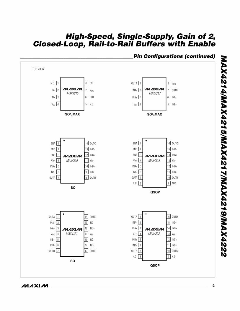
For pricing, delivery, and ordering information, please contact Maxim/Dallas Direct! at 1-888-629-4642, or visit Maxim’s website at www.maxim-ic.com. _________________General Description The MAX4214/MAX4215/MAX4217/MAX4219/MAX4222 are precision, closed-loop, gain of +2 (or -1) buffers featuring high slew rates, high output current drive, and low differential gain and phase error. They operate with a single 3.15V to 11V supply or with ±1.575V to ±5.5V dual supplies. The input common-mode voltage range extends 100mV beyond the negative power-supply rail, and the output swings Rail-to-Rail ® . These devices require only 5.5mA of quiescent supply current while achieving a 230MHz -3dB bandwidth and a 600V/μs slew rate. In addition, the MAX4215/ MAX4219 have a disable feature that reduces the sup- ply current to 400μA per buffer. Input voltage noise is only 10nV/ √ Hz, and input current noise is only 1.3pA/√Hz. This buffer family is ideal for low-power/low- voltage applications requiring wide bandwidth, such as video, communications, and instrumentation systems. For space-sensitive applications, the MAX4214 comes in a miniature 5-pin SOT23 package. ________________________Applications Battery-Powered Instruments Video Line Drivers Analog-to-Digital Converter Interface CCD Imaging Systems Video Routing and Switching Systems Video Multiplexing Applications ____________________________Features ♦ Internal Precision Resistors for Closed-Loop Gains of +2V/V or -1V/V ♦ High Speed 230MHz -3dB Bandwidth 90MHz 0.1dB Gain Flatness (MAX4219/MAX4222) 600V/μs Slew Rate ♦ Single 3.3V/5.0V Operation ♦ Outputs Swing Rail-to-Rail ♦ Input Common-Mode Range Extends Beyond V EE ♦ Low Differential Gain/Phase Error: 0.03%/0.04° ♦ Low Distortion at 5MHz -72dBc SFDR -71dB Total Harmonic Distortion ♦ High Output Drive: ±120mA ♦ Low 5.5mA Supply Current ♦ 400μA Shutdown Supply Current (MAX4215/MAX4219) ♦ Space-Saving SOT23, μMAX, or QSOP Packages MAX4214/MAX4215/MAX4217/MAX4219/MAX4222 High-Speed, Single-Supply, Gain of 2, Closed-Loop, Rail-to-Rail Buffers with Enable ________________________________________________________________ Maxim Integrated Products 1 V EE IN- IN+ 1 5 V CC OUT MAX4214 SOT23-5 TOP VIEW 2 3 4 19-4754; Rev 1; 8/01 PART MAX4214EUK-T MAX4215ESA MAX4215EUA -40°C to +85°C -40°C to +85°C -40°C to +85°C TEMP RANGE PIN- PACKAGE 5 SOT23-5 8 SO 8 μMAX Typical Application Circuit appears at end of data sheet. Rail-to-Rail is a registered trademark of Nippon Motorola, Ltd. Pin Configurations continued at end of data sheet. NO. OF AMPS ENABLE MAX4214 1 No MAX4215 1 Yes PART PIN-PACKAGE 5 SOT23 8 SO/μMAX MAX4217 2 No MAX4219 3 Yes 8 SO/μMAX 14 SO, 16 QSOP MAX4222 4 No 14 SO, 16 QSOP TOP MARK ABAH — — __________________Pin Configurations _______________Ordering Information ______________________Selector Guide MAX4217ESA MAX4217EUA -40°C to +85°C -40°C to +85°C 8 SO 8 μMAX — — MAX4219ESD MAX4219EEE -40°C to +85°C -40°C to +85°C 14 SO 16 QSOP — — MAX4222ESD MAX4222EEE -40°C to +85°C -40°C to +85°C 14 SO 16 QSOP — —
Transcript
For pricing, delivery, and ordering information, please contact Maxim/Dallas Direct! at 1-888-629-4642, or visit Maxim’s website at www.maxim-ic.com.
_________________General DescriptionThe MAX4214/MAX4215/MAX4217/MAX4219/MAX4222are precision, closed-loop, gain of +2 (or -1) buffersfeaturing high slew rates, high output current drive, andlow differential gain and phase error. They operate witha single 3.15V to 11V supply or with ±1.575V to ±5.5Vdual supplies. The input common-mode voltage rangeextends 100mV beyond the negative power-supply rail,and the output swings Rail-to-Rail®.
These devices require only 5.5mA of quiescent supplycurrent while achieving a 230MHz -3dB bandwidth anda 600V/µs slew rate. In addition, the MAX4215/MAX4219 have a disable feature that reduces the sup-ply current to 400µA per buffer. Input voltage noise isonly 10nV/√Hz, and input current noise is only1.3pA/√Hz. This buffer family is ideal for low-power/low-voltage applications requiring wide bandwidth, such asvideo, communications, and instrumentation systems.For space-sensitive applications, the MAX4214 comesin a miniature 5-pin SOT23 package.
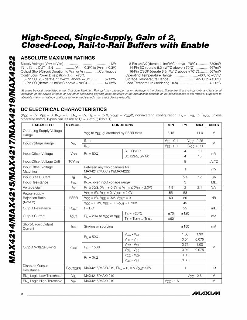
DC ELECTRICAL CHARACTERISTICS(VCC = 5V, VEE = 0, IN_- = 0, EN_ = 5V, RL = ∞ to 0, VOUT = VCC/2, noninverting configuration, TA = TMIN to TMAX, unless otherwise noted. Typical values are at TA = +25°C.) (Note 1)
Stresses beyond those listed under “Absolute Maximum Ratings” may cause permanent damage to the device. These are stress ratings only, and functionaloperation of the device at these or any other conditions beyond those indicated in the operational sections of the specifications is not implied. Exposure toabsolute maximum rating conditions for extended periods may affect device reliability.
Supply Voltage (VCC to VEE) ..................................................12VIN_-, IN_+, OUT_, EN_ ....................(VEE - 0.3V) to (VCC + 0.3V)Output Short-Circuit Duration to VCC or VEE..............ContinuousContinuous Power Dissipation (TA = +70°C)
Operating Temperature Range ...........................-40°C to +85°CStorage Temperature Range .............................-65°C to +150°CLead Temperature (soldering, 10s) .................................+300°C
VCC to VEE, guaranteed by PSRR tests
RL = 50Ω
3.15 11.0
±150
0.04 0.075
IN_-
SOT23-5, µMAX
VEE - 0.1 VCC + 0.1
SO, QSOP
VCC - VOH
IN_+
V
VEE - 0.1 VCC - 2.25
Operating Supply VoltageRange
Sinking or sourcing
VOL - VEE
VCC - VOH
VOL - VEE
VCC - VOH
IN_+, over input voltage range MΩ3
CONDITIONS
Between any two channels forMAX4217/MAX4219/MAX4222
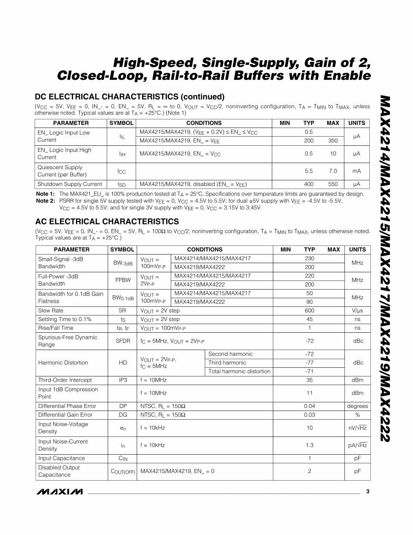
DC ELECTRICAL CHARACTERISTICS (continued)(VCC = 5V, VEE = 0, IN_- = 0, EN_ = 5V, RL = ∞ to 0, VOUT = VCC/2, noninverting configuration, TA = TMIN to TMAX, unless otherwise noted. Typical values are at TA = +25°C.) (Note 1)
AC ELECTRICAL CHARACTERISTICS(VCC = 5V, VEE = 0, IN_- = 0, EN_ = 5V, RL = 100Ω to VCC/2, noninverting configuration, TA = TMIN to TMAX, unless otherwise noted.Typical values are at TA = +25°C.)
CONDITIONS
mA5.5 7.0ICCQuiescent SupplyCurrent (per Buffer)
200 350MAX4215/MAX4219, EN_ = VEE
0.5 10
0.5
UNITSMIN TYP MAXSYMBOLPARAMETER
µA
µA
MAX4215/MAX4219, EN_ = VCC
MAX4215/MAX4219, (VEE + 0.2V) ≤ EN_ ≤ VCC
IIH
IIL
EN_ Logic Input HighCurrent
EN_ Logic Input LowCurrent
MAX4214/MAX4215/MAX4217
230
0.04
10
VOUT =2VP-P
MHz220
f = 10MHz
FPBWFull-Power -3dBBandwidth
MAX4214/MAX4215/MAX4217
200
NTSC, RL = 150Ω
MAX4214/MAX4215/MAX4217
MAX4219/MAX4222
MAX4219/MAX4222
MAX4219/MAX4222
VOUT = 100mVP-P ns1
CONDITIONS
VOUT = 2V step
200
Rise/Fall Time
VOUT = 2V step ns45tSSettling Time to 0.1%
V/µs600SRSlew Rate
VOUT =100mVP-P
BW-3dB
-72
dBc
Second harmonic
Small-Signal -3dBBandwidth
MHz
-71
fC = 5MHz, VOUT = 2VP-P
VOUT = 2VP-P, fC = 5MHz
-77
pF1
MAX4215/MAX4219, EN_ = 0
Third harmonic
2
CINInput Capacitance
Total harmonic distortion
35
dBc-72
tR, tF
SFDRSpurious-Free DynamicRange
90VOUT =100mVP-P
50BW0.1dB
Bandwidth for 0.1dB GainFlatness
MHz
f = 10MHzIP3
HD
Third-Order Intercept
Harmonic Distortion
dBm
COUT(OFF)
UNITSMIN TYP MAXSYMBOLPARAMETER
Disabled OutputCapacitance
pF
0.03
f = 10kHz
degrees
1.3
DPDifferential Phase Error
dBm11Input 1dB CompressionPoint
NTSC, RL = 150Ω
f = 10kHzin
en
DG
Input Noise-CurrentDensity
Input Noise-VoltageDensity
Differential Gain Error
pA/√Hz
nV/√Hz
%
MAX4215/MAX4219, disabled (EN_ = VEE) µA400 550ISDShutdown Supply Current
Note 1: The MAX421_EU_ is 100% production tested at TA = 25°C. Specifications over temperature limits are guaranteed by design.Note 2: PSRR for single 5V supply tested with VEE = 0, VCC = 4.5V to 5.5V; for dual ±5V supply with VEE = -4.5V to -5.5V,
VCC = 4.5V to 5.5V; and for single 3V supply with VEE = 0, VCC = 3.15V to 3.45V.
MA
X4
21
4/M
AX
42
15
/MA
X4
21
7/M
AX
42
19
/MA
X4
22
2
High-Speed, Single-Supply, Gain of 2, Closed-Loop, Rail-to-Rail Buffers with Enable
__________________________________________Typical Operating Characteristics(VCC = 5V, VEE = 0, AVCL = 2V/V, RL = 100Ω to VCC/2, TA = +25°C, unless otherwise noted.)
10
0100k 1M 10M 100M 1G
MAX4214/MAX4215/MAX4217SMALL-SIGNAL GAIN vs. FREQUENCY
2
MAX
4214
toc0
1
FREQUENCY (Hz)
GAIN
(dB)
4
6
8
9
1
3
5
7
VOUT = 100mVP-P
5.5100k 1M 10M 100M 1G
MAX4214/MAX4215/MAX4217GAIN FLATNESS vs. FREQUENCY
FREQUENCY (Hz)
5.6
6.5
5.7
MAX
4214
toc0
2
GAIN
(dB)
5.9
6.1
6.3
6.4
5.8
6.0
6.2
VOUT = 100mVP-P
10
0100k 1M 10M 100M 1G
MAX4214/MAX4215/MAX4217LARGE-SIGNAL GAIN vs. FREQUENCY
2
MAX
4214
toc0
3
FREQUENCY (Hz)
GAIN
(dB)
4
6
8
9
1
3
5
7
VOUT = 2VP-P
10
0100k 1M 10M 100M 1G
MAX4219/MAX4222SMALL-SIGNAL GAIN vs. FREQUENCY
2
MAX
4214
toc0
4
FREQUENCY (Hz)
GAIN
(dB)
4
6
8
9
1
3
5
7
VOUT = 100mVP-P
5.5100k 1M 10M 100M 1G
MAX4219/MAX4222GAIN FLATNESS vs. FREQUENCY
FREQUENCY (Hz)
5.6
6.5
5.7
MAX
4214
toc0
5
GAIN
(dB)
5.9
6.1
6.3
6.4
5.8
6.0
6.2
VOUT = 100mVP-P10
0100k 1M 10M 100M 1G
MAX4219/MAX4222LARGE-SIGNAL GAIN vs. FREQUENCY
2
MAX
4214
toc0
6
FREQUENCY (Hz)
GAIN
(dB)
4
6
8
9
1
3
5
7
VOUT = 2VP-PRL = 100Ω
AC ELECTRICAL CHARACTERISTICS (continued)(VCC = 5V, VEE = 0, IN_- = 0, EN_ = 5V, RL = 100Ω to VCC/2, noninverting configuration, TA = TMIN to TMAX, unless otherwise noted.Typical values are at TA = +25°C.)
All-Hostile Crosstalk XTALKMAX4217/MAX4219/MAX4222, f = 10MHz, VOUT = 2VP-P
dB
PARAMETER SYMBOL MIN TYP MAX UNITS
Buffer Enable Time tON 100 ns
-95
Buffer Gain Matching dBMAX4217/MAX4219/MAX4222, f = 10MHz, VOUT = 100mVP-P
MAX4215/MAX4219
0.1
Buffer Disable Time tOFF 1 µsMAX4215/MAX4219
Output Impedance ZOUT 200 mΩf = 10MHz
CONDITIONS
0
-100100k 1M 10M 100M
HARMONIC DISTORTION vs. FREQUENCY
-80
MAX
4214
toc0
7
FREQUENCY (Hz)
HARM
ONIC
DIS
TORT
ION
(dBc
)
-60
-40
-20
-10
-90
-70
-50
-30
VOUT = 2VP-P
2ND HARMONIC
3RD HARMONIC
0
-1000 100 200 300 400 500 600 700 800 900 1k
HARMONIC DISTORTION vs. RESISTIVE LOAD
-80
MAX
4214
toc0
8
RESISTIVE LOAD (Ω)
HARM
ONIC
DIS
TORT
ION
(dBc
)
-60
-40
-20
-10
-90
-70
-50
-30
VOUT = 2VP-Pf = 5MHz
2ND HARMONIC
3RD HARMONIC
0
-1000.5 1.0 1.5 2.0 2.5 3.0 3.5
HARMONIC DISTORTION vs. VOLTAGE SWING
-80
MAX
4214
toc0
9
VOLTAGE SWING (Vp-p)
HARM
ONIC
DIS
TORT
ION
(dBc
)
-60
-40
-20
-10
-90
-70
-50
-30
f = 5MHz
2ND HARMONIC
3RD HARMONIC
MA
X4
21
4/M
AX
42
15
/MA
X4
21
7/M
AX
42
19
/MA
X4
22
2
High-Speed, Single-Supply, Gain of 2, Closed-Loop, Rail-to-Rail Buffers with Enable
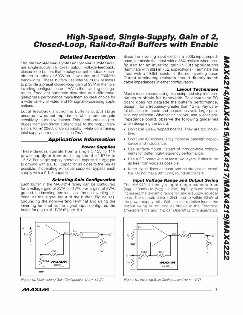
________________Detailed DescriptionThe MAX4214/MAX4215/MAX4217/MAX4219/MAX4222are single-supply, rail-to-rail output, voltage-feedback,closed-loop buffers that employ current-feedback tech-niques to achieve 600V/µs slew rates and 230MHzbandwidths. These buffers use internal 500Ω resistorsto provide a preset closed-loop gain of 2V/V in the non-inverting configuration or -1V/V in the inverting configu-ration. Excellent harmonic distortion and differentialgain/phase performance make them an ideal choice fora wide variety of video and RF signal-processing appli-cations.
Local feedback around the buffer’s output stageensures low output impedance, which reduces gainsensitivity to load variations. This feedback also pro-duces demand-driven current bias to the output tran-sistors for ±120mA drive capability, while constrainingtotal supply current to less than 7mA.
___________Applications InformationPower Supplies
These devices operate from a single 3.15V to 11Vpower supply or from dual supplies of ±1.575V to±5.5V. For single-supply operation, bypass the VCC pinto ground with a 0.1µF capacitor as close to the pin aspossible. If operating with dual supplies, bypass eachsupply with a 0.1µF capacitor.
Selecting Gain ConfigurationEach buffer in the MAX4214 family can be configuredfor a voltage gain of 2V/V or -1V/V. For a gain of 2V/V,ground the inverting terminal. Use the noninverting ter-minal as the signal input of the buffer (Figure 1a).Grounding the noninverting terminal and using theinverting terminal as the signal input configures thebuffer for a gain of -1V/V (Figure 1b).
Since the inverting input exhibits a 500Ω input imped-ance, terminate the input with a 56Ω resistor when con-figured for an inverting gain in 50Ω applications(terminate with 88Ω in 75Ω applications). Terminate theinput with a 49.9Ω resistor in the noninverting case.Output terminating resistors should directly matchcable impedances in either configuration.
Layout TechniquesMaxim recommends using microstrip and stripline tech-niques to obtain full bandwidth. To ensure the PCboard does not degrade the buffer’s performance,design it for a frequency greater than 1GHz. Pay care-ful attention to inputs and outputs to avoid large para-sitic capacitance. Whether or not you use a constant-impedance board, observe the following guidelineswhen designing the board:
• Don’t use wire-wrapped boards. They are too induc-tive.
• Don’t use IC sockets. They increase parasitic capac-itance and inductance.
• Use surface-mount instead of through-hole compo-nents for better high-frequency performance.
• Use a PC board with at least two layers; it should beas free from voids as possible.
• Keep signal lines as short and as straight as possi-ble. Do not make 90° turns; round all corners.
Input Voltage Range and Output SwingThe MAX4214 family’s input range extends from (VEE - 100mV) to (VCC - 2.25V). Input ground sensingincreases the dynamic range for single-supply applica-tions. The outputs drive a 2kΩ load to within 60mV ofthe power-supply rails. With smaller resistive loads, theoutput swing is reduced as shown in the ElectricalCharacteristics and Typical Operating Characteristics.
MA
X4
21
4/M
AX
42
15
/MA
X4
21
7/M
AX
42
19
/MA
X4
22
2
High-Speed, Single-Supply, Gain of 2,Closed-Loop, Rail-to-Rail Buffers with Enable
Figure 1a. Noninverting Gain Configuration (AV = +2V/V)
MAX42_ _
500Ω 500Ω
OUT
RO
RTOOUTRS
RTIN
IN+
IN-IN
Figure 1b. Inverting Gain Configuration (AV = -1V/V)
MA
X4
21
4/M
AX
42
15
/MA
X4
21
7/M
AX
42
19
/MA
X4
22
2 As the load resistance decreases, the useful input rangeis effectively limited by the output drive capability, sincethe buffers have a fixed voltage gain of 2V/V or -1V/V.
For example, a 50Ω load can typically be driven from40mV above VEE to 1.6V below VCC, or 40mV to 3.4Vwhen operating from a single 5V supply. If the buffer isoperated in the noninverting, gain of 2V/V configurationwith the inverting input grounded, the useful input volt-age range becomes 20mV to 1.7V instead of the -100mV to 2.75V indicated by the Electrical Character-istics. Beyond the useful input range, the buffer outputis a nonlinear function of the input, but it will not under-go phase reversal or latchup.
EnableThe MAX4215/MAX4219 have an enable feature (EN_)that allows the buffer to be placed in a low-power state.When the buffers are disabled, the supply current isreduced to 400µA per buffer.
As the voltage at the EN_ pin approaches the negativesupply rail, the EN_ input current rises. Figure 2 showsa graph of EN_ input current versus EN_ pin voltage.Figure 3 shows the addition of an optional resistor inseries with the EN pin, to limit the magnitude of the cur-rent increase. Figure 4 displays the resulting EN pininput current to voltage relationship.
Disabled Output ResistanceThe MAX4214/MAX4215/MAX4217/MAX4219/MAX4222include internal protection circuitry that prevents dam-age to the precision input stage from large differentialinput voltages (Figure 5). This protection circuitry con-
sists of five back-to-back Schottky diodes betweenIN_+ and IN_-. These diodes reduce the disabled out-put resistance from 1kΩ to 500Ω when the output volt-age is 3V greater or less than the voltage at IN_+.Under these conditions, the input protection diodes willbe forward biased, lowering the disabled output resis-tance to 500Ω.
Output Capacitive Loading and StabilityThe MAX4214 family provides maximum AC perfor-mance with no load capacitance. This is the case whenthe load is a properly terminated transmission line.These devices are designed to drive up to 20pF of loadcapacitance without oscillating, but AC performancewill be reduced under these conditions.
High-Speed, Single-Supply, Gain of 2,Closed-Loop, Rail-to-Rail Buffers with Enable
Figure 2. Enable Logic-Low Input Current vs. Enable Logic-Low Threshold
OUT
IN-
EN_IN+
10kΩ
ENABLE
500Ω 500Ω
MAX42_ _
Figure 3. Circuit to Reduce Enable Logic-Low Input Current
0
-100 100 300 500
-7
-8
-1
VIL (mV ABOVE VEE)
INPU
T CU
RREN
T (µ
A)
200 400
-3
-5
-9
-2
-4
-6
Figure 4. Enable Logic-Low Input Current vs. Enable Logic-Low Threshold with 10kΩ Series Resistor
Driving large capacitive loads increases the chance ofoscillations occurring in most amplifier circuits. This isespecially true for circuits with high loop gains, such asvoltage followers. The buffer’s output resistance and theload capacitor combine to add a pole and excess phaseto the loop response. If the frequency of this pole is lowenough to interfere with the loop response and degradephase margin sufficiently, oscillations can occur.
A second problem when driving capacitive loadsresults from the amplifier’s output impedance, whichlooks inductive at high frequencies. This inductanceforms an L-C resonant circuit with the capacitive load,which causes peaking in the frequency response anddegrades the amplifier’s gain margin.
Figure 6 shows the devices’ frequency response underdifferent capacitive loads. To drive loads with greaterthan 20pF of capacitance or to settle out some of the peaking, the output requires an isolation resistorlike the one shown in Figure 7. Figure 8 is a graph ofthe Optimal Isolation Resistor vs. Load Capacitance.Figure 9 shows the frequency response of theMAX4214/MAX4215/MAX4217/MAX4219/MAX4222when driving capacitive loads with a 27Ω isolationresistor.
Coaxial cables and other transmission lines are easilydriven when properly terminated at both ends with theircharacteristic impedance. Driving back-terminatedtransmission lines essentially eliminates the lines’capacitance.
MA
X4
21
4/M
AX
42
15
/MA
X4
21
7/M
AX
42
19
/MA
X4
22
2
High-Speed, Single-Supply, Gain of 2,Closed-Loop, Rail-to-Rail Buffers with Enable
__________________________________________________Tape-and-Reel Information
SO
T5L.
EP
S
P
DE
F
WP2P0
D1
A0
B0
K0
t
±0.102
±0.102
A0
B0
D
D1
3.200
3.099
1.499
0.991
±0.102
±0.051
±0.102
±0.102
1.753
3.505
1.397
3.988
E
F
K0
P
+0.102+0.000
NOTE: DIMENSIONS ARE IN MM.AND FOLLOW EIA481-1 STANDARD.
+0.305 -0.102
+0.254+0.000
P0 3.988 ±0.102
P010 40.005 ±0.203
P2 2.007 ±0.051
t 0.254 ±0.127
W 8.001
5 S
OT
23-5
Package Information(The package drawing(s) in this data sheet may not reflect the most current specifications. For the latest package outline information,go to www.maxim-ic.com/packages.)
MA
X4
21
4/M
AX
42
15
/MA
X4
21
7/M
AX
42
19
/MA
X4
22
2
High-Speed, Single-Supply, Gain of 2,Closed-Loop, Rail-to-Rail Buffers with Enable
Package Information (continued)(The package drawing(s) in this data sheet may not reflect the most current specifications. For the latest package outline information,go to www.maxim-ic.com/packages.)
MA
X4
21
4/M
AX
42
15
/MA
X4
21
7/M
AX
42
19
/MA
X4
22
2
High-Speed, Single-Supply, Gain of 2,Closed-Loop, Rail-to-Rail Buffers with Enable
Maxim cannot assume responsibility for use of any circuitry other than circuitry entirely embodied in a Maxim product. No circuit patent licenses areimplied. Maxim reserves the right to change the circuitry and specifications without notice at any time.
16 ____________________Maxim Integrated Products, 120 San Gabriel Drive, Sunnyvale, CA 94086 408-737-7600
Package Information (continued)(The package drawing(s) in this data sheet may not reflect the most current specifications. For the latest package outline information,go to www.maxim-ic.com/packages.)