23
High Step-up Flying Capacitor Multilevel Converters Zitao Liao ECE590 March 27, 2017

High Step-up Flying Capacitor Multilevel Converters
Zitao LiaoECE590
March 27, 2017
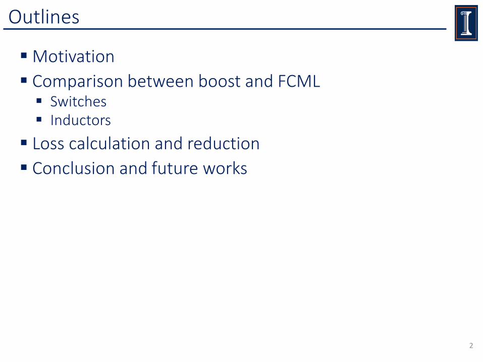
Outlines
▪Motivation
▪ Comparison between boost and FCML▪ Switches▪ Inductors
▪ Loss calculation and reduction
▪ Conclusion and future works
2
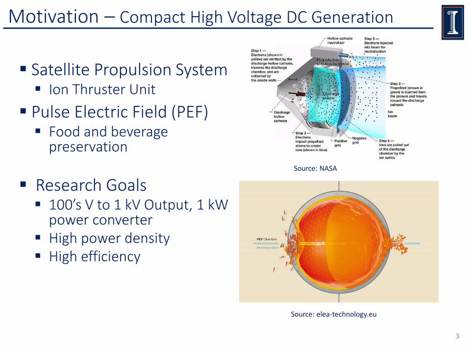
Motivation – Compact High Voltage DC Generation
▪ Satellite Propulsion System▪ Ion Thruster Unit
▪ Pulse Electric Field (PEF)▪ Food and beverage
preservation
▪ Research Goals▪ 100’s V to 1 kV Output, 1 kW
power converter▪ High power density▪ High efficiency
3
Source: elea-technology.eu
Source: NASA

Boost converters- switches
4
IL∆𝐼𝐿
𝐷𝑇𝑠𝑤 𝑇𝑠𝑤
VL
𝐼𝑖𝑛
𝑉𝑖𝑛
𝑉𝑖𝑛 − 𝑉𝑜𝑢𝑡
IL →
+ -
𝐷𝑇𝑠𝑤 𝑇𝑠𝑤
Vout
▪ 1 kV, 10 A
▪ High blocking voltage:▪ Large Rds_on -> conduction loss▪ Large Qg, Qoss-> switching loss
▪ Thermal ▪ Hard to cool a single hot spot
▪ Availability?
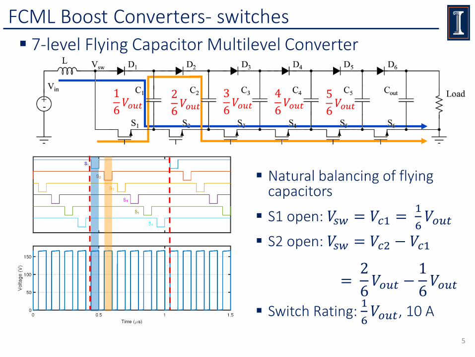
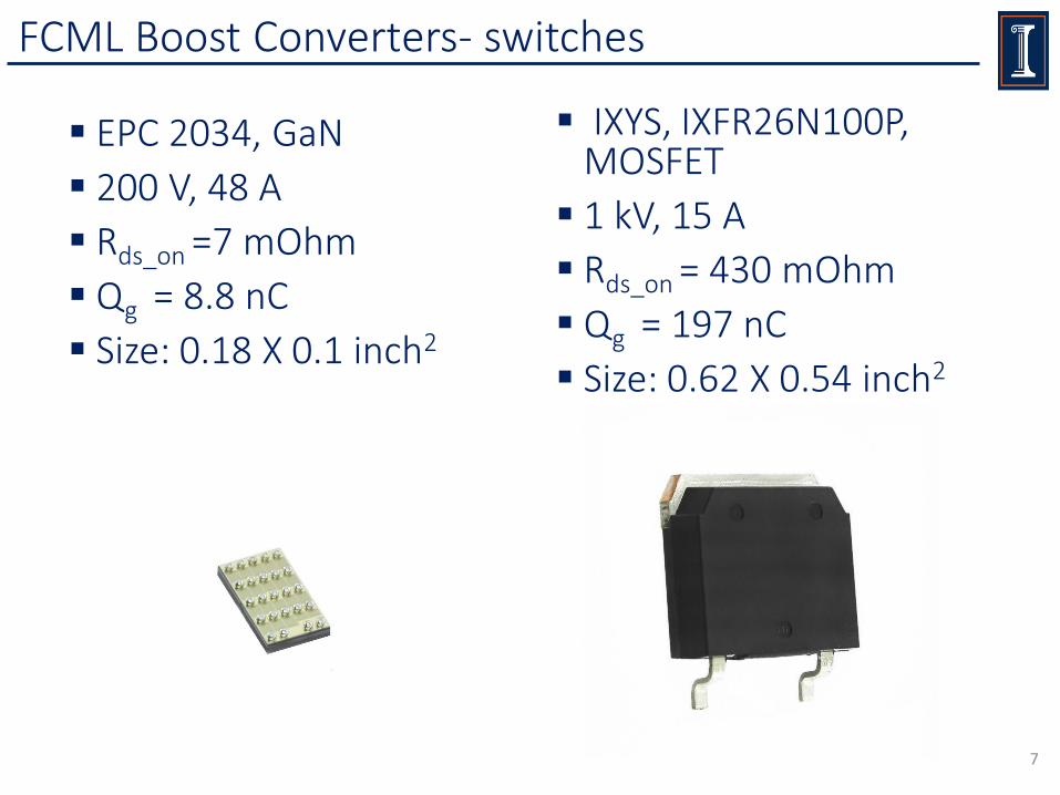
FCML Boost Converters- switches
5
1
6𝑉𝑜𝑢𝑡
2
6𝑉𝑜𝑢𝑡
3
6𝑉𝑜𝑢𝑡
4
6𝑉𝑜𝑢𝑡
5
6𝑉𝑜𝑢𝑡
▪ Natural balancing of flying capacitors
▪ S1 open: 𝑉𝑠𝑤 = 𝑉𝑐1 =1
6𝑉𝑜𝑢𝑡
▪ S2 open: 𝑉𝑠𝑤 = 𝑉𝑐2 − 𝑉𝑐1
=2
6𝑉𝑜𝑢𝑡 −
1
6𝑉𝑜𝑢𝑡
▪ Switch Rating: 1
6𝑉𝑜𝑢𝑡, 10 A
▪ 7-level Flying Capacitor Multilevel Converter
▪ 166 V, 10 A
▪ Lower voltage rating:▪ Lower Rds_on▪ Lower Qg
▪ Thermal▪ Heat is distributed to more switches
▪ Availability▪ More likely to find in stock…
6
FCML Boost Converters- switches
FCML Boost Converters- switches
▪ EPC 2034, GaN
▪ 200 V, 48 A
▪ Rds_on =7 mOhm
▪ Qg = 8.8 nC
▪ Size: 0.18 X 0.1 inch2
7
▪ IXYS, IXFR26N100P, MOSFET
▪ 1 kV, 15 A
▪ Rds_on = 430 mOhm
▪ Qg = 197 nC
▪ Size: 0.62 X 0.54 inch2
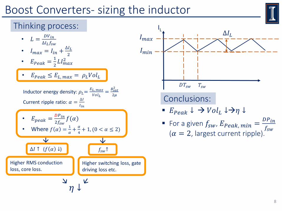
Boost Converters- sizing the inductor
8
IL∆𝐼𝐿
𝐷𝑇𝑠𝑤 𝑇𝑠𝑤
𝐼𝑚𝑎𝑥
𝐼𝑚𝑖𝑛
• 𝐿 =𝐷𝑉𝑖𝑛
∆𝐼𝐿𝑓𝑠𝑤
• 𝐼𝑚𝑎𝑥 = 𝐼𝑖𝑛 +∆𝐼𝐿
2
• 𝐸𝑃𝑒𝑎𝑘 =1
2𝐿𝐼𝑚𝑎𝑥
2
• 𝐸𝑃𝑒𝑎𝑘 ≤ 𝐸𝐿, 𝑚𝑎𝑥 = 𝜌𝐿𝑉𝑜𝑙𝐿
Higher switching loss, gate driving loss etc.
Higher RMS conduction loss, core loss.
𝑓𝑠𝑤↑
→ →
𝜂 ↓
• 𝐸𝑝𝑒𝑎𝑘 =𝐷𝑃𝑖𝑛
2𝑓𝑠𝑤𝑓(𝛼)
• Where 𝑓 𝛼 =1
𝛼+
𝛼
4+ 1, (0 < 𝛼 ≤ 2)
Inductor energy density: 𝜌𝐿=𝐸𝐿, 𝑚𝑎𝑥
𝑉𝑜𝑙𝐿=
𝐵𝑠𝑎𝑡2
2𝜇
Current ripple ratio: 𝛼 =∆𝐼
𝐼𝑖𝑛
∆𝐼 ↑ (𝑓 𝛼 ↓)
▪ 𝐸𝑃𝑒𝑎𝑘 ↓ → 𝑉𝑜𝑙𝐿 ↓→𝜂 ↓
▪ For a given 𝑓𝑠𝑤, 𝐸𝑃𝑒𝑎𝑘, 𝑚𝑖𝑛 =𝐷𝑃𝑖𝑛
𝑓𝑠𝑤(𝛼 = 2, largest current ripple).
Thinking process:
Conclusions:

FCML Boost Converter- sizing the inductor
9
▪ 7-level Flying Capacitor Multilevel Converter
▪ 𝐸𝑝𝑒𝑎𝑘, 𝑏𝑜𝑜𝑠𝑡 =𝐷𝑃𝑖𝑛
2𝑓𝑠𝑤𝑓 𝛼
0
0.2
0.4
0.6
0.8
1
2 3 4 5 6 7 8 9 10
Norm
aliz
ed I
nduct
or
Volu
me
FCML Level
Normalized Inductor Size v.s. FCML Level
(D=0.9)
13.5x reduction
Total Passive Component Volume
1
6𝑉𝑜𝑢𝑡
2
6𝑉𝑜𝑢𝑡
3
6𝑉𝑜𝑢𝑡
4
6𝑉𝑜𝑢𝑡
5
6𝑉𝑜𝑢𝑡
→ 𝐸𝑝𝑒𝑎𝑘, 𝑓𝑐𝑚𝑙 =1 − 1 − 𝐷 𝑁 − 1 𝑃𝑖𝑛
2𝑓𝑠𝑤 𝑁 − 1𝑓(𝛼)
Y. Lei, W-C Liu, R.C.N. Pilawa-Podgurski, “An Analytical Method to Evaluate and Design Hybrid Switched-Capacitor and Multilevel Converters,” IEEE Transactions on Power Electronics, in press
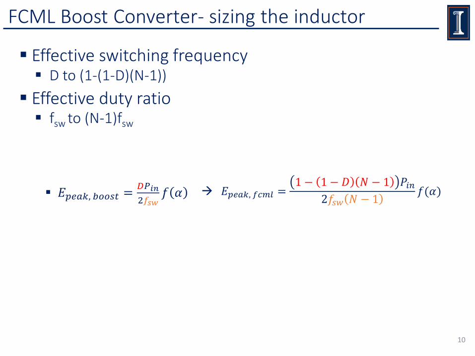
▪ Effective switching frequency ▪ D to (1-(1-D)(N-1))
▪ Effective duty ratio▪ fsw to (N-1)fsw
10
▪ 𝐸𝑝𝑒𝑎𝑘, 𝑏𝑜𝑜𝑠𝑡 =𝐷𝑃𝑖𝑛
2𝑓𝑠𝑤𝑓 𝛼 → 𝐸𝑝𝑒𝑎𝑘, 𝑓𝑐𝑚𝑙 =
1 − 1 − 𝐷 𝑁 − 1 𝑃𝑖𝑛2𝑓𝑠𝑤 𝑁 − 1
𝑓(𝛼)
FCML Boost Converter- sizing the inductor
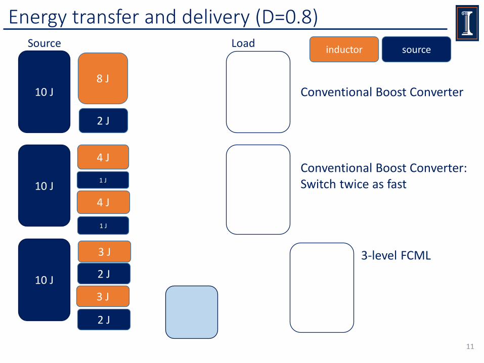
Energy transfer and delivery (D=0.8)
11
10 J 8 J
2 J
10 J
4 J
1 J
10 J
3 J
4 J
1 J
2 J
3 J
2 J
Source Load
Conventional Boost Converter
Conventional Boost Converter:Switch twice as fast
inductor source
3-level FCML

Hardware Prototype
12
DiodesGaNSwitches
Isolated DC-DC for gate drivers
Flying capacitorsInductor Digital Isolators
Input
Input
Z. Liao, Y. Lei and R.C.N. Pilawa-Podgurski “A GaN-based Flying-Capacitor Multilevel Boost Converter for High Step-up Conversion,” IEEE Energy Conversion Congress and Exposition, Milwaukee, WI, 2016
Loss distribution
▪ Conduction loss▪ Rds_on ,diode Ron and inductor DCR
▪ Switching loss▪ Overlap loss and reverse recovery loss
▪ Inductor core loss▪ Current ripple and switching frequency
13
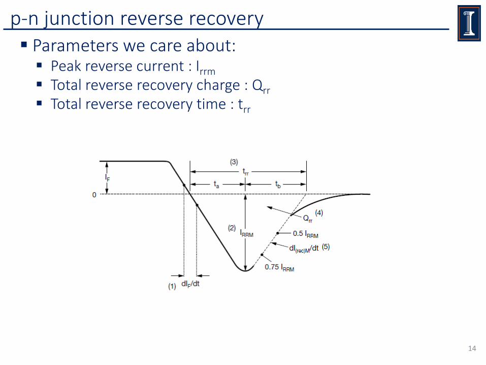
p-n junction reverse recovery ▪ Parameters we care about:▪ Peak reverse current : Irrm
▪ Total reverse recovery charge : Qrr
▪ Total reverse recovery time : trr
14

Diodes in hard-switched boost converters
15
Vsw
Ifet
t0 t2 t4
𝑊𝑟𝑟 = 𝑉𝑠𝑤 𝑡𝑟𝑟𝐼𝑖𝑛 + 𝑄𝑟𝑟 𝑓𝑠𝑤
𝐸𝑟𝑟 = 𝑉𝑠𝑤𝐼𝑖𝑛𝑡𝑟𝑟 + 𝑉𝑠𝑤𝑄𝑟𝑟
▪ Reverse recovery increases switching loss because:▪ Longer switching transition: trr
▪ Extra charge: Qrr
Iin
Qrr
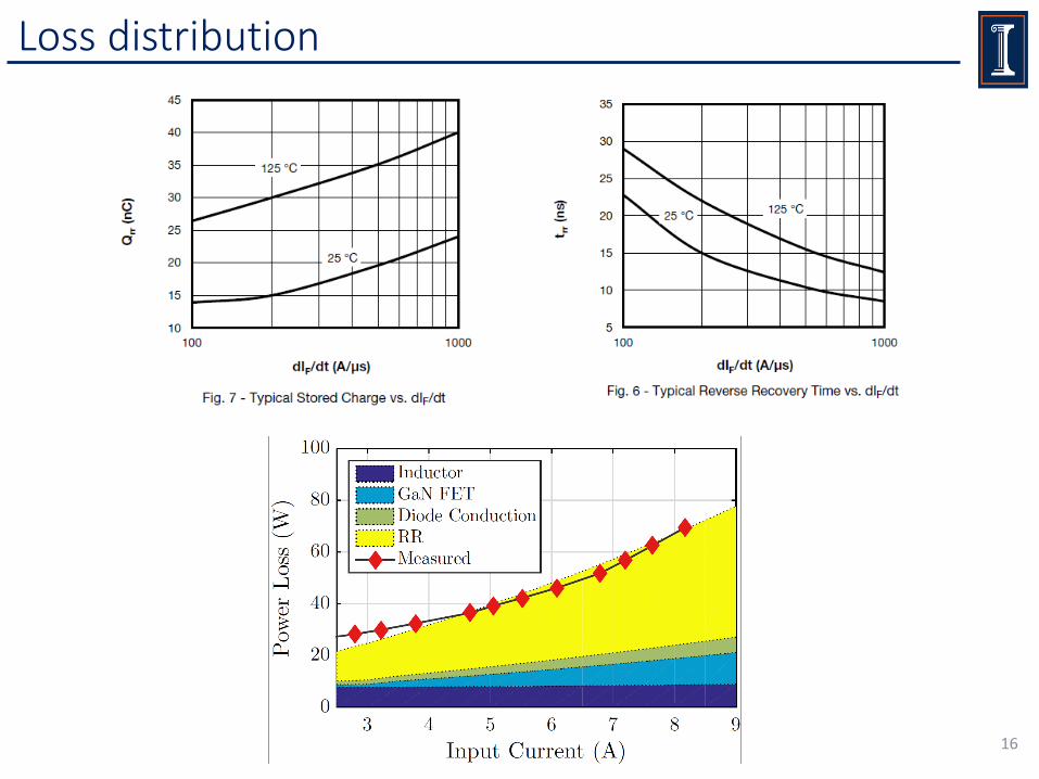
Loss distribution
16

Reduction of reverse recovery
▪ Parallel diodes
17
▪ Both Qrr and trr increase with temperature
▪ Temperature increases with input current
▪ Wrr∝ IinN
, (N>1). Paralleling diode should reduce Wrr .
▪ I assumed linear relationship between 𝑄𝑟𝑟, 𝑡𝑟𝑟 and Iin, so N = 2
𝑊𝑟𝑟 = 𝑉𝑜𝑢𝑡 𝑡𝑟𝑟𝐼𝑖𝑛 + 𝑄𝑟𝑟 𝑓𝑠𝑤𝑄𝑟𝑟, 𝑡𝑟𝑟 ∝ 𝐼𝑖𝑛
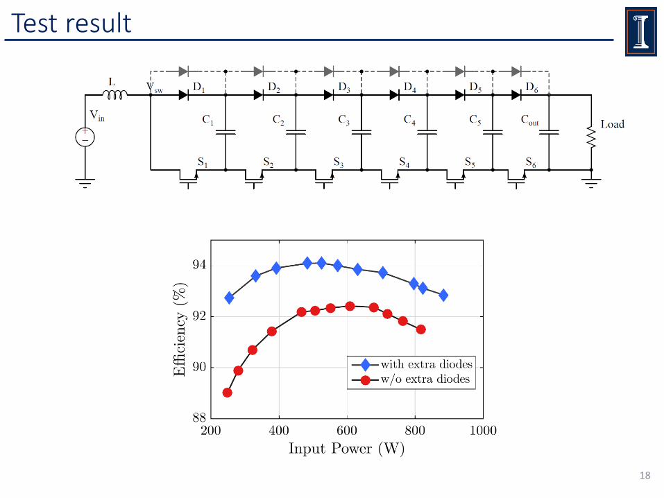
Test result
18
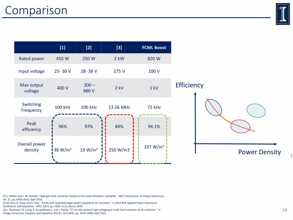
Comparison
19
[1] [2] [3] FCML Boost
Rated power 450 W 250 W 2 kW 820 W
Input voltage 25- 30 V 28- 38 V 275 V 100 V
Max outputvoltage
400 V300 –980 V
2 kV 1 kV
Switching Frequency
100 kHz 100 kHz 13.56 MHz 72 kHz
Peak efficiency
96% 97% 84% 94.1%
Overall powerdensity 38 W/in3 19 W/in3 250 W/in3
337 W/in3
19Power Density
Efficiency
[1] L. Müller and J. W. Kimball, “High gain dcdc converter based on the cockcroftwalton multiplier,” IEEE Transactions on Power Electronics,vol. 31, pp. 6405–6415, Sept 2016.[2] M. Kim, D. Yang, and S. Choi, “A fully soft-switched single switch isolated dc-dc converter,” in 2014 IEEE Applied Power ElectronicsConference and Exposition - APEC 2014, pp. 1106–1111, March 2014.[3] L. Raymond, W. Liang, K. Surakitbovorn, and J. Davila, “27.12 mhz isolated high voltage gain multi-level resonant dc-dc converter,” inEnergy Conversion Congress and Exposition (ECCE), 2015 IEEE, pp. 5074–5080, Sept 2015.
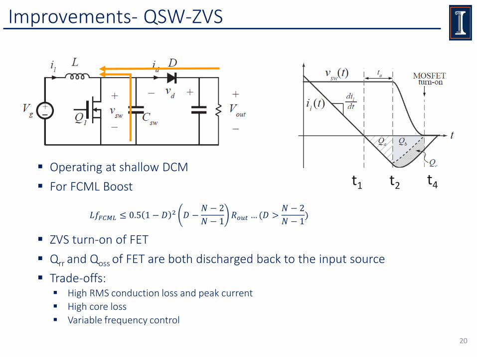
Improvements- QSW-ZVS
20
t1 t2 t4
▪ ZVS turn-on of FET
▪ Qrr and Qoss of FET are both discharged back to the input source
▪ Trade-offs:▪ High RMS conduction loss and peak current
▪ High core loss
▪ Variable frequency control
▪ Operating at shallow DCM
▪ For FCML Boost
𝐿𝑓𝐹𝐶𝑀𝐿 ≤ 0.5 1 − 𝐷 2 𝐷 −𝑁 − 2
𝑁 − 1𝑅𝑜𝑢𝑡 …(𝐷 >
𝑁 − 2
𝑁 − 1)

QSW-ZVS
21
Hard-Switching QSW-ZVS
Pin= 108.68 WPout= 101.99 WSwitching Frequency: 69 kHzInductor: 4 uH
Pin = 106 WPout = 100 WSwitching Frequency: 72 kHzInductor: 22 uH
▪ Switches are cooler: switching loss ↓ > conduction loss ↑
▪ Need better inductor design for lower core loss

Conclusions
▪ FCML:▪ Lower rating device▪ Smaller inductor
▪ Improvements:▪ Soft-switching techniques▪ Better inductor design
22
23
Thank you!


![[5]the Age of Multilevel Converters Arrives](https://static.documents.pub/doc/80x56/553318214a795998578b47e1/5the-age-of-multilevel-converters-arrives.jpg)


