DESCRIPTIONThe OPA547 is a low-cost, high-voltage/high-current opera-tional amplifier ideal for driving a wide variety of loads. Alaser-trimmed monolithic integrated circuit provides excellentlow-level signal accuracy and high output voltage and cur-rent.
The OPA547 operates from either single or dual supplies fordesign flexibility. In single-supply operation, the input com-mon-mode range extends below ground.
The OPA547 is internally protected against over-temperatureconditions and current overloads. In addition, the OPA547was designed to provide an accurate, user-selected currentlimit. Unlike other designs which use a “power” resistor inseries with the output current path, the OPA547 senses theload indirectly. This allows the current limit to be adjustedfrom 0mA to 750mA with a 0 to 150µA control signal. This iseasily done with a resistor/potentiometer or controlled digi-tally with a voltage-out or current-out DAC.
The Enable/Status (E/S) pin provides two functions. An inputon the pin not only disables the output stage to effectivelydisconnect the load, but also reduces the quiescent currentto conserve power. The E/S pin output can be monitored todetermine if the OPA547 is in thermal shutdown.
The OPA547 is available in an industry-standard7-lead staggered and straight lead TO-220 package, and a7-lead DDPAK surface-mount plastic power package. Thecopper tab allows easy mounting to a heat sink or circuitboard for excellent thermal performance. It is specified foroperation over the extended industrial temperature range,–40°C to +85°C.
FEATURES WIDE SUPPLY RANGE
Single Supply: +8V to +60VDual Supply: ±4V to ±30V
HIGH OUTPUT CURRENT:500mA Continuous
WIDE OUTPUT VOLTAGE SWING
FULLY PROTECTED:Thermal ShutdownAdjustable Current Limit
OUTPUT DISABLE CONTROL
THERMAL SHUTDOWN INDICATOR
HIGH SLEW RATE: 6V/µs
LOW QUIESCENT CURRENT
PACKAGES:7-Lead TO-220, Zip and Straight Leads7-Lead DDPAK Surface-Mount
APPLICATIONS VALVE, ACTUATOR DRIVERS
SYNCHRO, SERVO DRIVERS
POWER SUPPLIES
TEST EQUIPMENT
TRANSDUCER EXCITATION
AUDIO AMPLIFIERS
OPA547
VIN–
VIN+
V+
E/S
RCL
RCL sets the current limitvalue from 0 to 750mA.
(1/4 Watt Resistor)
ILIM
VO
V–
OPA547
SBOS056F – JANUARY 2002 – JULY 2005
www.ti.com
PRODUCTION DATA information is current as of publication date.Products conform to specifications per the terms of Texas Instrumentsstandard warranty. Production processing does not necessarily includetesting of all parameters.
Please be aware that an important notice concerning availability, standard warranty, and use in critical applications ofTexas Instruments semiconductor products and disclaimers thereto appears at the end of this data sheet.
OPA547
OPA547 OPA547
OPA5472SBOS056Fwww.ti.com
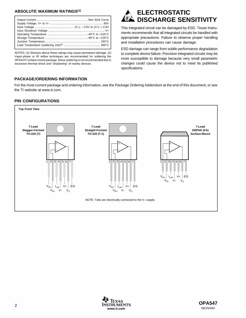
ABSOLUTE MAXIMUM RATINGS(1)
Output Current ................................................................. See SOA CurveSupply Voltage, V+ to V– ................................................................... 60VInput Voltage .................................................. (V–) – 0.5V to (V+) + 0.5VInput Shutdown Voltage ........................................................................ V+Operating Temperature .................................................. –40°C to +125°CStorage Temperature ..................................................... –55°C to +125°CJunction Temperature ...................................................................... 150°CLead Temperature (soldering 10s)(2) .............................................. 300°C
Top Front View
PIN CONFIGURATIONS
NOTES: (1) Stresses above these ratings may cause permanent damage. (2)Vapor-phase or IR reflow techniques are recommended for soldering theOPA547F surface-mount package. Wave soldering is not recommended due toexcessive thermal shock and “shadowing” of nearby devices.
PACKAGE/ORDERING INFORMATION
For the most current package and ordering information, see the Package Ordering Addendum at the end of this document, or seethe TI website at www.ti.com.
ELECTROSTATICDISCHARGE SENSITIVITY
This integrated circuit can be damaged by ESD. Texas Instru-ments recommends that all integrated circuits be handled withappropriate precautions. Failure to observe proper handlingand installation procedures can cause damage.
ESD damage can range from subtle performance degradationto complete device failure. Precision integrated circuits may bemore susceptible to damage because very small parametricchanges could cause the device not to meet its publishedspecifications.
7-LeadStraight-Formed
TO-220 (T-1)
NOTE: Tabs are electrically connected to the V– supply.
ILIM
V– VO
V+VIN–
VIN+
1 2 3 4 5 6
E/S
7
7-LeadDDPAK (FA)
Surface-Mount
ILIM
V– VO
V+VIN–
VIN+
1 2 3 4 5 6
E/S
7
7-LeadStagger-Formed
TO-220 (T)
ILIM
V– VO
V+VIN–
VIN+
1 2 3 4 5 6
E/S
7
OPA547 3SBOS056F www.ti.com
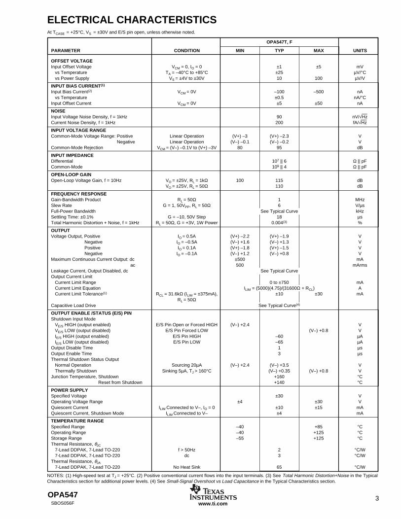
ELECTRICAL CHARACTERISTICSAt TCASE = +25°C, VS = ±30V and E/S pin open, unless otherwise noted.
VE/S HIGH (output enabled) E/S Pin Open or Forced HIGH (V–) +2.4 VVE/S LOW (output disabled) E/S Pin Forced LOW (V–) +0.8 VIE/S HIGH (output enabled) E/S Pin HIGH –60 µAIE/S LOW (output disabled) E/S Pin LOW –65 µA
Output Disable Time 1 µsOutput Enable Time 3 µsThermal Shutdown Status Output
Normal Operation Sourcing 20µA (V–) +2.4 (V–) +3.5 VThermally Shutdown Sinking 5µA, TJ > 160°C (V–) +0.35 (V–) +0.8 V
Junction Temperature, Shutdown +160 °CReset from Shutdown +140 °C
POWER SUPPLYSpecified Voltage ±30 VOperating Voltage Range ±4 ±30 VQuiescent Current ILIM Connected to V–, IO = 0 ±10 ±15 mAQuiescent Current, Shutdown Mode ILIM Connected to V– ±4 mA
TEMPERATURE RANGESpecified Range –40 +85 °COperating Range –40 +125 °CStorage Range –55 +125 °CThermal Resistance, θJC
7-Lead DDPAK, 7-Lead TO-220 f > 50Hz 2 °C/W7-Lead DDPAK, 7-Lead TO-220 dc 3 °C/W
NOTES: (1) High-speed test at TJ = +25°C. (2) Positive conventional current flows into the input terminals. (3) See Total Harmonic Distortion+Noise in the TypicalCharacteristics section for additional power levels. (4) See Small-Signal Overshoot vs Load Capacitance in the Typical Characteristics section.
OPA5474SBOS056Fwww.ti.com
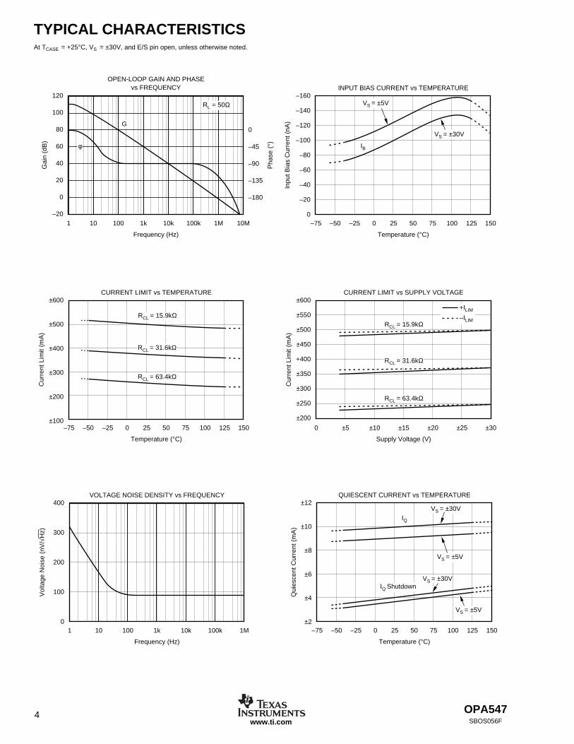
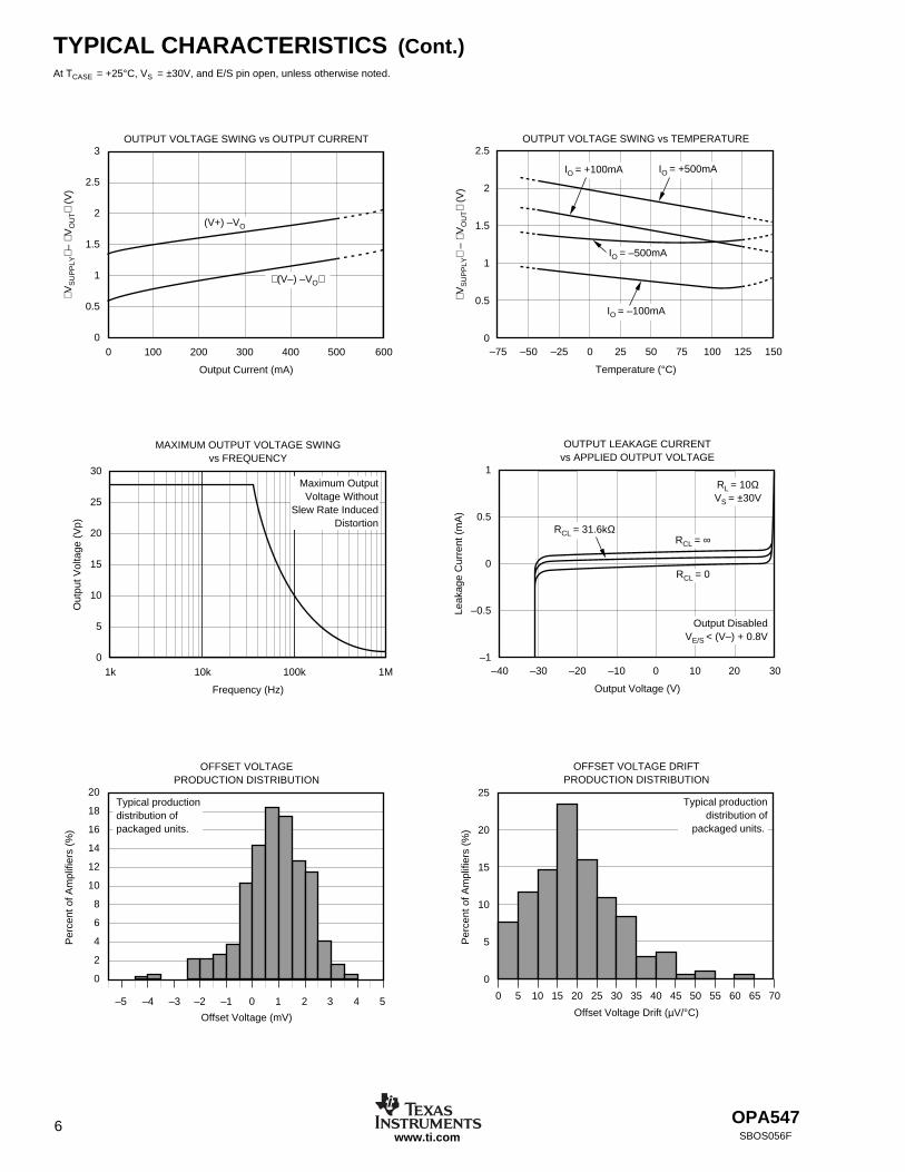
TYPICAL CHARACTERISTICSAt TCASE = +25°C, VS = ±30V, and E/S pin open, unless otherwise noted.
1 10 100 1k 10k 100k 1M 10M
120
100
80
60
40
20
0
–20
Gai
n (d
B)
0
–45
–90
–135
–180
Pha
se (
°)
Frequency (Hz)
OPEN-LOOP GAIN AND PHASEvs FREQUENCY
RL = 50Ω
G
φ
–75 –50 –25 0 25 50 75 100 125 150
–160
–140
–120
–100
–80
–60
–40
–20
0
Inpu
t Bia
s C
urre
nt (
nA)
Temperature (°C)
INPUT BIAS CURRENT vs TEMPERATURE
IB
VS = ±5V
VS = ±30V
–75 –50 –25 0 25 50 75 100 125 150
±600
±500
±400
±300
±200
±100
Cur
rent
Lim
it (m
A)
Temperature (°C)
CURRENT LIMIT vs TEMPERATURE
RCL = 31.6kΩ
RCL = 63.4kΩ
RCL = 15.9kΩ
0 ±5 ±10 ±15 ±20 ±25 ±30
±600
±550
±500
±450
+400
±350
±300
±250
±200
Cur
rent
Lim
it (m
A)
Supply Voltage (V)
CURRENT LIMIT vs SUPPLY VOLTAGE
RCL = 15.9kΩ
RCL = 31.6kΩ
RCL = 63.4kΩ
+ILIM
–ILIM
1 10 100 1k 10k 100k 1M
400
300
200
100
0
Vol
tage
Noi
se (
nV/√
Hz)
Frequency (Hz)
VOLTAGE NOISE DENSITY vs FREQUENCY
–75 –50 –25 0 25 50 75 100 125 150
±12
±10
±8
±6
±4
±2
Qui
esce
nt C
urre
nt (
mA
)
Temperature (°C)
QUIESCENT CURRENT vs TEMPERATURE
IQ
IQ Shutdown
VS = ±30V
VS = ±5V
VS = ±30V
VS = ±5V
OPA547 5SBOS056F www.ti.com
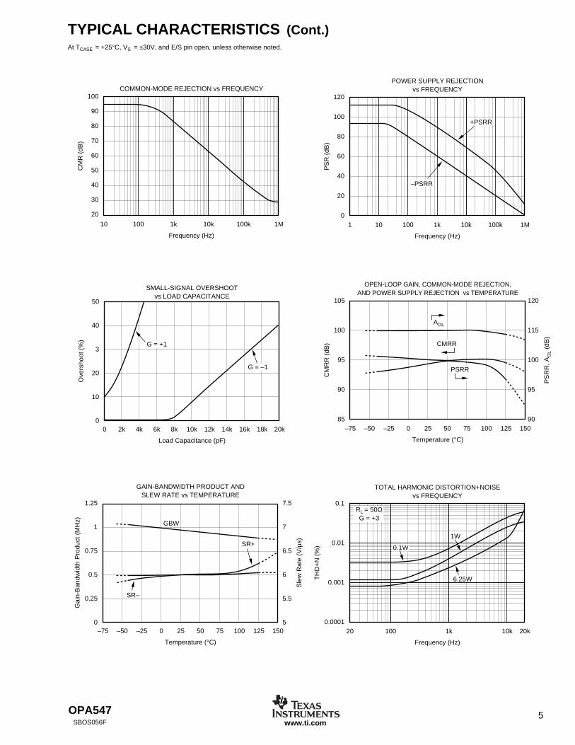
TYPICAL CHARACTERISTICS (Cont.)At TCASE = +25°C, VS = ±30V, and E/S pin open, unless otherwise noted.
10 100 1k 10k 100k 1M
100
90
80
70
60
50
40
30
20
CM
R (
dB)
Frequency (Hz)
COMMON-MODE REJECTION vs FREQUENCY
1 10 100 1k 10k 100k 1M
120
100
80
60
40
20
0
PS
R (
dB)
Frequency (Hz)
POWER SUPPLY REJECTIONvs FREQUENCY
+PSRR
–PSRR
0 2k 4k 6k 8k 10k 12k 14k 16k 18k 20k
50
40
3
20
10
0
Ove
rsho
ot (
%)
Load Capacitance (pF)
SMALL-SIGNAL OVERSHOOTvs LOAD CAPACITANCE
G = –1
G = +1
–75 –50 –25 0
AOL
25 50 75 100 125 150
105
100
95
90
85
CM
RR
(dB
)
120
115
100
95
90
PS
RR
, AO
L (d
B)
Temperature (°C)
OPEN-LOOP GAIN, COMMON-MODE REJECTION,AND POWER SUPPLY REJECTION vs TEMPERATURE
CMRR
PSRR
–75 –50 –25 0 25 50 75 100 125 150
1.25
1
0.75
0.5
0.25
0
7.5
7
6.5
6
5.5
5
Gai
n-B
andw
idth
Pro
duct
(M
Hz)
Sle
w R
ate
(V/µ
s)
Temperature (°C)
GAIN-BANDWIDTH PRODUCT ANDSLEW RATE vs TEMPERATURE
SR+
SR–
GBW
20 100 1k 10k 20k
0.1
0.01
0.001
0.0001
TH
D+
N (
%)
Frequency (Hz)
TOTAL HARMONIC DISTORTION+NOISEvs FREQUENCY
RL = 50ΩG = +3
0.1W
1W
6.25W
OPA5476SBOS056Fwww.ti.com
TYPICAL CHARACTERISTICS (Cont.)At TCASE = +25°C, VS = ±30V, and E/S pin open, unless otherwise noted.
0 100 200 300 400 500 600
3
2.5
2
1.5
1
0.5
0
VS
UP
PLY
–
VO
UT
(V)
Output Current (mA)
OUTPUT VOLTAGE SWING vs OUTPUT CURRENT
(V+) –VO
(V–) –VO
–75 –50 –25 0 25 50 75 100 125 150
2.5
2
1.5
1
0.5
0
VS
UP
PLY
–
VO
UT
(V)
Temperature (°C)
OUTPUT VOLTAGE SWING vs TEMPERATURE
IO = +500mAIO = +100mA
IO = –500mA
IO = –100mA
1k 10k 100k 1M
30
25
20
15
10
5
0
Out
put V
olta
ge (
Vp)
Frequency (Hz)
MAXIMUM OUTPUT VOLTAGE SWINGvs FREQUENCY
Maximum OutputVoltage Without
Slew Rate InducedDistortion
–40 –30 –20 –10 0 10 20 30
1
0.5
0
–0.5
–1
Leak
age
Cur
rent
(m
A)
Output Voltage (V)
OUTPUT LEAKAGE CURRENTvs APPLIED OUTPUT VOLTAGE
RCL = 31.6kΩRCL = ∞
RCL = 0
RL = 10ΩVS = ±30V
Output DisabledVE/S < (V–) + 0.8V
OFFSET VOLTAGEPRODUCTION DISTRIBUTION
Per
cent
of A
mpl
ifier
s (%
)
Offset Voltage (mV)
20
18
16
14
12
10
8
6
4
2
0
Typical productiondistribution ofpackaged units.
–5 –4 –2–3 –1 0 1 2 3 4 5
OFFSET VOLTAGE DRIFTPRODUCTION DISTRIBUTION
Per
cent
of A
mpl
ifier
s (%
)
Offset Voltage Drift (µV/°C)
25
20
15
10
5
0
Typical productiondistribution of
packaged units.
0 5 10 15 20 25 30 35 40 45 50 55 60 65 70
OPA547 7SBOS056F www.ti.com
5µs/div
LARGE SIGNAL STEP RESPONSEG = 3, CL = 100pF, RL = 50Ω
SMALL SIGNAL STEP RESPONSEG = 3, CL = 1000pF
TYPICAL CHARACTERISTICS (Cont.)At TCASE = +25°C, VS = ±35V, and E/S pin open, unless otherwise noted.
50m
V/d
iv
2µs/div
50m
V/d
iv
2µs/div10
V/d
iv
SMALL SIGNAL STEP RESPONSEG = 1, CL = 1000pF
OPA5478SBOS056Fwww.ti.com
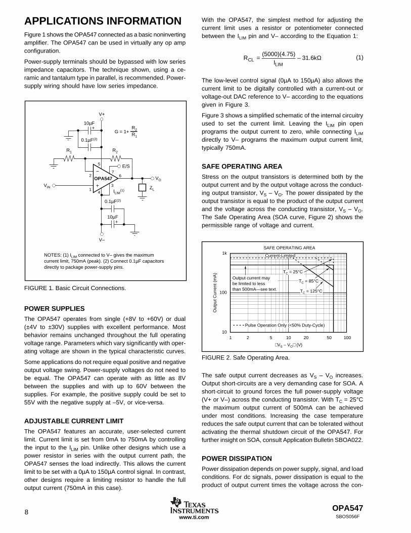
APPLICATIONS INFORMATIONFigure 1 shows the OPA547 connected as a basic noninvertingamplifier. The OPA547 can be used in virtually any op ampconfiguration.
Power-supply terminals should be bypassed with low seriesimpedance capacitors. The technique shown, using a ce-ramic and tantalum type in parallel, is recommended. Power-supply wiring should have low series impedance.
G = 1+ R2
R1
ZL
E/S
3
7
5
4
2
1
6
R2
ILIM(1)
R1
0.1µF(2)
10µF
OPA547
V–
V+
+
+
VIN
10µF
0.1µF(2)
VO
NOTES: (1) ILIM connected to V– gives the maximum current limit, 750mA (peak). (2) Connect 0.1µF capacitors directly to package power-supply pins.
With the OPA547, the simplest method for adjusting thecurrent limit uses a resistor or potentiometer connectedbetween the ILIM pin and V– according to the Equation 1:
RI
kCLLIM
= ( )( . )– .
5000 4 7531 6 Ω
The low-level control signal (0µA to 150µA) also allows thecurrent limit to be digitally controlled with a current-out orvoltage-out DAC reference to V– according to the equationsgiven in Figure 3.
Figure 3 shows a simplified schematic of the internal circuitryused to set the current limit. Leaving the ILIM pin openprograms the output current to zero, while connecting ILIM
directly to V– programs the maximum output current limit,typically 750mA.
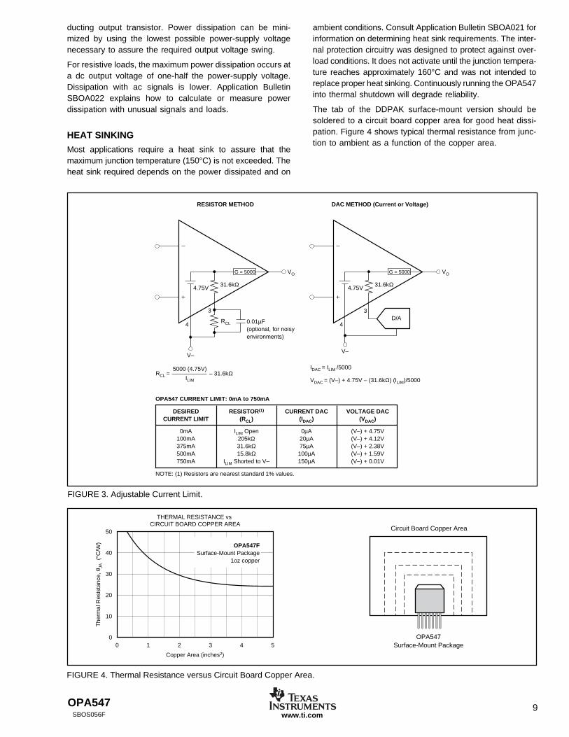
SAFE OPERATING AREA
Stress on the output transistors is determined both by theoutput current and by the output voltage across the conduct-ing output transistor, VS – VO. The power dissipated by theoutput transistor is equal to the product of the output currentand the voltage across the conducting transistor, VS – VO.The Safe Operating Area (SOA curve, Figure 2) shows thepermissible range of voltage and current.
FIGURE 1. Basic Circuit Connections.
POWER SUPPLIES
The OPA547 operates from single (+8V to +60V) or dual(±4V to ±30V) supplies with excellent performance. Mostbehavior remains unchanged throughout the full operatingvoltage range. Parameters which vary significantly with oper-ating voltage are shown in the typical characteristic curves.
Some applications do not require equal positive and negativeoutput voltage swing. Power-supply voltages do not need tobe equal. The OPA547 can operate with as little as 8Vbetween the supplies and with up to 60V between thesupplies. For example, the positive supply could be set to55V with the negative supply at –5V, or vice-versa.
ADJUSTABLE CURRENT LIMIT
The OPA547 features an accurate, user-selected currentlimit. Current limit is set from 0mA to 750mA by controllingthe input to the ILIM pin. Unlike other designs which use apower resistor in series with the output current path, theOPA547 senses the load indirectly. This allows the currentlimit to be set with a 0µA to 150µA control signal. In contrast,other designs require a limiting resistor to handle the fulloutput current (750mA in this case).
1 2 5 10
VS – VO (V)
20 50 100
SAFE OPERATING AREA1k
100
Out
put C
urre
nt (
mA
)
10
Current-Limited
TC = 25°C
TC = 125°C
TC = 85°COutput current maybe limited to lessthan 500mA—see text.
Pulse Operation Only (<50% Duty-Cycle)
FIGURE 2. Safe Operating Area.
The safe output current decreases as VS – VO increases.Output short-circuits are a very demanding case for SOA. Ashort-circuit to ground forces the full power-supply voltage(V+ or V–) across the conducting transistor. With TC = 25°Cthe maximum output current of 500mA can be achievedunder most conditions. Increasing the case temperaturereduces the safe output current that can be tolerated withoutactivating the thermal shutdown circuit of the OPA547. Forfurther insight on SOA, consult Application Bulletin SBOA022.
POWER DISSIPATION
Power dissipation depends on power supply, signal, and loadconditions. For dc signals, power dissipation is equal to theproduct of output current times the voltage across the con-
(1)
OPA547 9SBOS056F www.ti.com
ducting output transistor. Power dissipation can be mini-mized by using the lowest possible power-supply voltagenecessary to assure the required output voltage swing.
For resistive loads, the maximum power dissipation occurs ata dc output voltage of one-half the power-supply voltage.Dissipation with ac signals is lower. Application BulletinSBOA022 explains how to calculate or measure powerdissipation with unusual signals and loads.
HEAT SINKING
Most applications require a heat sink to assure that themaximum junction temperature (150°C) is not exceeded. Theheat sink required depends on the power dissipated and on
ambient conditions. Consult Application Bulletin SBOA021 forinformation on determining heat sink requirements. The inter-nal protection circuitry was designed to protect against over-load conditions. It does not activate until the junction tempera-ture reaches approximately 160°C and was not intended toreplace proper heat sinking. Continuously running the OPA547into thermal shutdown will degrade reliability.
The tab of the DDPAK surface-mount version should besoldered to a circuit board copper area for good heat dissi-pation. Figure 4 shows typical thermal resistance from junc-tion to ambient as a function of the copper area.
FIGURE 4. Thermal Resistance versus Circuit Board Copper Area.
THERMAL RESISTANCE vs CIRCUIT BOARD COPPER AREA
50
40
30
20
10
0
The
rmal
Res
ista
nce,
θJA
(°C
/W)
0 1 2 3 4 5
Copper Area (inches2)
OPA547FSurface-Mount Package
1oz copper
Circuit Board Copper Area
OPA547Surface-Mount Package
FIGURE 3. Adjustable Current Limit.
31.6kΩ
RCL 0.01µF(optional, for noisyenvironments)
3
4
3
4
4.75V
G = 5000
RCL = – 31.6kΩ
OPA547 CURRENT LIMIT: 0mA to 750mA
NOTE: (1) Resistors are nearest standard 1% values.
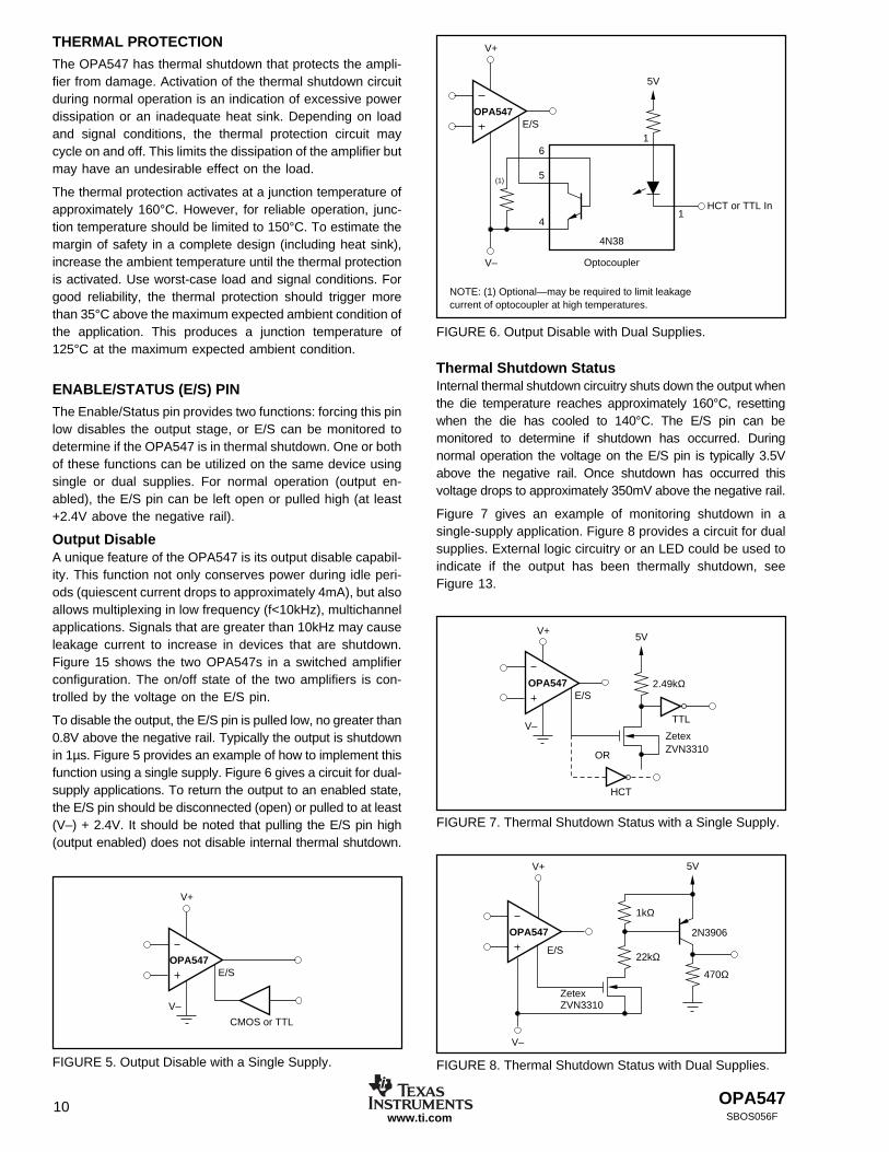
The OPA547 has thermal shutdown that protects the ampli-fier from damage. Activation of the thermal shutdown circuitduring normal operation is an indication of excessive powerdissipation or an inadequate heat sink. Depending on loadand signal conditions, the thermal protection circuit maycycle on and off. This limits the dissipation of the amplifier butmay have an undesirable effect on the load.
The thermal protection activates at a junction temperature ofapproximately 160°C. However, for reliable operation, junc-tion temperature should be limited to 150°C. To estimate themargin of safety in a complete design (including heat sink),increase the ambient temperature until the thermal protectionis activated. Use worst-case load and signal conditions. Forgood reliability, the thermal protection should trigger morethan 35°C above the maximum expected ambient condition ofthe application. This produces a junction temperature of125°C at the maximum expected ambient condition.
ENABLE/STATUS (E/S) PIN
The Enable/Status pin provides two functions: forcing this pinlow disables the output stage, or E/S can be monitored todetermine if the OPA547 is in thermal shutdown. One or bothof these functions can be utilized on the same device usingsingle or dual supplies. For normal operation (output en-abled), the E/S pin can be left open or pulled high (at least+2.4V above the negative rail).
Output DisableA unique feature of the OPA547 is its output disable capabil-ity. This function not only conserves power during idle peri-ods (quiescent current drops to approximately 4mA), but alsoallows multiplexing in low frequency (f<10kHz), multichannelapplications. Signals that are greater than 10kHz may causeleakage current to increase in devices that are shutdown.Figure 15 shows the two OPA547s in a switched amplifierconfiguration. The on/off state of the two amplifiers is con-trolled by the voltage on the E/S pin.
To disable the output, the E/S pin is pulled low, no greater than0.8V above the negative rail. Typically the output is shutdownin 1µs. Figure 5 provides an example of how to implement thisfunction using a single supply. Figure 6 gives a circuit for dual-supply applications. To return the output to an enabled state,the E/S pin should be disconnected (open) or pulled to at least(V–) + 2.4V. It should be noted that pulling the E/S pin high(output enabled) does not disable internal thermal shutdown.
OPA547
V+
E/S
V–
NOTE: (1) Optional—may be required to limit leakagecurrent of optocoupler at high temperatures.
(1)
61
1
4N38
Optocoupler
5
4
HCT or TTL In
5V
FIGURE 6. Output Disable with Dual Supplies.
Thermal Shutdown StatusInternal thermal shutdown circuitry shuts down the output whenthe die temperature reaches approximately 160°C, resettingwhen the die has cooled to 140°C. The E/S pin can bemonitored to determine if shutdown has occurred. Duringnormal operation the voltage on the E/S pin is typically 3.5Vabove the negative rail. Once shutdown has occurred thisvoltage drops to approximately 350mV above the negative rail.
Figure 7 gives an example of monitoring shutdown in asingle-supply application. Figure 8 provides a circuit for dualsupplies. External logic circuitry or an LED could be used toindicate if the output has been thermally shutdown, seeFigure 13.
FIGURE 7. Thermal Shutdown Status with a Single Supply.
FIGURE 8. Thermal Shutdown Status with Dual Supplies.FIGURE 5. Output Disable with a Single Supply.
OPA547
V+
E/S
HCT
OR
TTL
2.49kΩ
ZetexZVN3310
5V
V–
OPA547
V+
E/S
V–
1kΩ
5V
22kΩ
470Ω
2N3906
ZetexZVN3310
OPA547
V+
E/S
V–
CMOS or TTL
OPA547 11SBOS056F www.ti.com
Output Disable and Thermal Shutdown StatusAs mentioned earlier, the OPA547’s output can be disabledand the disable status can be monitored simultaneously.Figures 9 and 10 provide examples using a single supply anddual supplies, respectively.
OPA547
V+
E/S
Open Drain(Output Disable)
HCT(Thermal Status
Shutdown)
V–
FIGURE 9. Output Disable and Thermal Shutdown Status witha Single Supply.
OUTPUT PROTECTION
Reactive and EMF-generating loads can return load cur-rent to the amplifier, causing the output voltage to exceedthe power-supply voltage. This damaging condition can beavoided with clamp diodes from the output terminal to thepower supplies, as shown in Figure 11. Schottkey rectifierdiodes with a 1A or greater continuous rating are recom-mended.
FIGURE 10. Output Disable and Thermal Shutdown Status with Dual Supplies.
FIGURE 11. Motor Drive Circuit.
G = – = –4R2
R1
3Ω(Carbon)
0.01µF
R220kΩ
R15kΩ
OPA547
V–
V+
VIN
Motor
D1
D2
D1, D2 : International Rectifier 11DQ06.
OPA547
V+
E/S
NOTE: (1) Optional—may be required to limit leakagecurrent of optocoupler at high temperatures.
V–
(1)
61
2
4N38
Optocoupler
5
4
HCT or TTL In
5V 6
2
1
4N38
Optocoupler
5
4Zetex
ZVN3310
TTL Out7.5kΩ1W
5V
OUTPUT STAGE COMPENSATION
The complex load impedances common in power op ampapplications can cause output stage instability. For normaloperation output compensation circuitry is not typically re-quired. However, if the OPA547 is intended to be driven intocurrent limit, a R/C network may be required. Figure 11shows an output series R/C compensation (snubber) net-work (3Ω in series with 0.01µF) which generally providesexcellent stability. Some variations in circuit values may berequired with certain loads.
OPA54712SBOS056Fwww.ti.com
VOLTAGE SOURCE APPLICATION
Figure 12 illustrates how to use the OPA547 to provide anaccurate voltage source with only three external resistors.First, the current limit resistor, RCL, is chosen according tothe desired output current. The resulting voltage at the ILIM
pin is constant and stable over temperature. This voltage,VCL, is connected to the noninverting input of the op amp andused as a voltage reference, thus eliminating the need for anexternal reference. The feedback resistors are selected togain VCL to the desired output voltage level.
FIGURE 13. Resistor-Controlled Programmable Power Supply.
FIGURE 12. Voltage Source.
31.6kΩ
RCL
ILIM
0.01µF(Optional, for noisyenvironments)
4.75V
IO =5000 (4.75V)
31.6kΩ + RCL
VO = VCL (1 + R2/R1)
V–
V+
VCL
VCL = = 2.375V
Desired VO = 19V,
R1 = 1kΩ and R2 = 7kΩ
G = = 819
2.375
For Example:
31.6kΩ • 4.75V
(31.6kΩ + 31.6kΩ)
If ILIM = 375mA, RCL = 31.6kΩ
R2R1
Uses voltage developed at ILIM pin as a moderately accurate reference voltage.
PROGRAMMABLE POWER SUPPLY
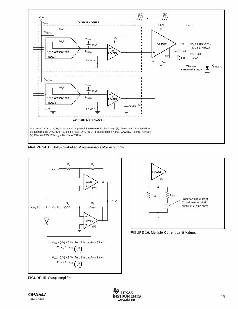
A programmable power supply can easily be built using theOPA547. Both the output voltage and output current areuser-controlled. Figure 13 shows a circuit using potentiom-eters to adjust the output voltage and current while Figure 14uses DACs. An LED tied to the E/S pin through a logic gateindicates if the OPA547 is in thermal shutdown.
G = 1 + = 109kΩ1kΩ
9kΩ1kΩ
OPA547
+30V+5V
+5V
0.8V to 2.5V
0V to 4.75V
OutputAdjust
V+5
6
ThermalShutdown Status
NOTES: (1) For VO = 0V, V– = –1V.(2) Optional: Improves noiseimmunity.
(LED)
74HCT04 R ≥ 250Ω
E/SVO = 0.8V to 25V(1)
74
3
1
2
V–
ILIM
14.7kΩ
4.7kΩ
CurrentLimit
Adjust
1kΩ
20kΩ 0.01µF(2)
OPA547 13SBOS056F www.ti.com
DAC B
1/2 DAC7800/1/2(3)
1/2 DAC7800/1/2(3)
10pF
IOUT B
RFB B
AGND B0.01µF(2)
ILIM
ThermalShutdown Status
(LED)
74HCT04R ≥ 250Ω
9kΩ1kΩ
VO = 0.8 to 25V(1)
IO = 0 to 750mA
G = 10
V–
E/SDAC A
+5V
+5V
VREF B
DGND
10pF
IOUT A
RFB A
OUTPUT ADJUST
OPA547
CURRENT LIMIT ADJUST
AGND A
+30V
VREF A
NOTES: (1) For VO = 0V, V– = –1V. (2) Optional, improves noise immunity. (3) Chose DAC780X based on digital interface: DAC7800—12-bit interface, DAC7801—8-bit interface + 4 bits, DAC7802—serial interface. (4) Can use OPA2237, IO = 100mA to 750mA.
1/2OPA2336
1/2OPA2336
VREF
+10V
FIGURE 14. Digitally-Controlled Programmable Power Supply.
FIGURE 16. Multiple Current Limit Values.
OPA547
RC2RC1
Close for high current(Could be open drainoutput of a logic gate).
ILIM
V–
( )
E/S
R2R1
VIN1
AMP1
VO
E/S
R4R3
VE/S > (V–) +2.4V: Amp 1 is on, Amp 2 if off
VO = –VIN1 R2
R1
VE/S VIN2
AMP2
( )VE/S < (V–) +2.4V: Amp 2 is on, Amp 1 if off
VO = –VIN2 R4
R3
FIGURE 15. Swap Amplifier.
PACKAGING INFORMATION
Orderable Device Status (1) PackageType
PackageDrawing
Pins PackageQty
Eco Plan (2) Lead/Ball Finish MSL Peak Temp (3)
OPA547F OBSOLETE DDPAK KTW 7 TBD Call TI Call TI
OPA547F/500 ACTIVE DDPAK KTW 7 500 Green (RoHS &no Sb/Br)
CU SN Level-2-260C-1 YEAR
OPA547F/500G3 ACTIVE DDPAK KTW 7 500 Green (RoHS &no Sb/Br)
CU SN Level-2-260C-1 YEAR
OPA547FKTWT ACTIVE DDPAK KTW 7 50 Green (RoHS &no Sb/Br)
CU SN Level-2-260C-1 YEAR
OPA547FKTWTG3 ACTIVE DDPAK KTW 7 50 Green (RoHS &no Sb/Br)
CU SN Level-2-260C-1 YEAR
OPA547T ACTIVE TO-220 KVT 7 50 Green (RoHS &no Sb/Br)
CU SN N / A for Pkg Type
OPA547T-1 ACTIVE TO-220 KC 7 50 Green (RoHS &no Sb/Br)
CU SN N / A for Pkg Type
OPA547T-1G3 ACTIVE TO-220 KC 7 50 Green (RoHS &no Sb/Br)
CU SN N / A for Pkg Type
OPA547TG3 ACTIVE TO-220 KVT 7 50 Green (RoHS &no Sb/Br)
CU SN N / A for Pkg Type
(1) The marketing status values are defined as follows:ACTIVE: Product device recommended for new designs.LIFEBUY: TI has announced that the device will be discontinued, and a lifetime-buy period is in effect.NRND: Not recommended for new designs. Device is in production to support existing customers, but TI does not recommend using this part ina new design.PREVIEW: Device has been announced but is not in production. Samples may or may not be available.OBSOLETE: TI has discontinued the production of the device.
(2) Eco Plan - The planned eco-friendly classification: Pb-Free (RoHS), Pb-Free (RoHS Exempt), or Green (RoHS & no Sb/Br) - please checkhttp://www.ti.com/productcontent for the latest availability information and additional product content details.TBD: The Pb-Free/Green conversion plan has not been defined.Pb-Free (RoHS): TI's terms "Lead-Free" or "Pb-Free" mean semiconductor products that are compatible with the current RoHS requirementsfor all 6 substances, including the requirement that lead not exceed 0.1% by weight in homogeneous materials. Where designed to be solderedat high temperatures, TI Pb-Free products are suitable for use in specified lead-free processes.Pb-Free (RoHS Exempt): This component has a RoHS exemption for either 1) lead-based flip-chip solder bumps used between the die andpackage, or 2) lead-based die adhesive used between the die and leadframe. The component is otherwise considered Pb-Free (RoHScompatible) as defined above.Green (RoHS & no Sb/Br): TI defines "Green" to mean Pb-Free (RoHS compatible), and free of Bromine (Br) and Antimony (Sb) based flameretardants (Br or Sb do not exceed 0.1% by weight in homogeneous material)
(3) MSL, Peak Temp. -- The Moisture Sensitivity Level rating according to the JEDEC industry standard classifications, and peak soldertemperature.
Important Information and Disclaimer:The information provided on this page represents TI's knowledge and belief as of the date that it isprovided. TI bases its knowledge and belief on information provided by third parties, and makes no representation or warranty as to theaccuracy of such information. Efforts are underway to better integrate information from third parties. TI has taken and continues to takereasonable steps to provide representative and accurate information but may not have conducted destructive testing or chemical analysis onincoming materials and chemicals. TI and TI suppliers consider certain information to be proprietary, and thus CAS numbers and other limitedinformation may not be available for release.
In no event shall TI's liability arising out of such information exceed the total purchase price of the TI part(s) at issue in this document sold by TIto Customer on an annual basis.
NOTES: A. All linear dimensions are in inches (millimeters).B. This drawing is subject to change without notice.
C. Lead width and height dimensions apply to theplated lead.
D. Leads are not allowed above the Datum B.E. Stand–off height is measured from lead tip
with reference to Datum B.F. Lead width dimension does not include dambar
protrusion. Allowable dambar protrusion shall notcause the lead width to exceed the maximumdimension by more than 0.003”.
G. Cross–hatch indicates exposed metal surface.
H. Falls within JEDEC MO–169 with the exceptionof the dimensions indicated.
MECHANICAL DATA
MSOT010 – OCTOBER 1994
1POST OFFICE BOX 655303 • DALLAS, TEXAS 75265
KC (R-PSFM-T7) PLASTIC FLANGE-MOUNT PACKAGE
4040251/B 01/95
0.420 (10,67)
0.055 (1,40)
0.335 (8,51)
0.030 (0,76)0.026 (0,66)
0.380 (9,65)
0.325 (8,25)
0.045 (1,14)0.113 (2,87)0.103 (2,62)
0.146 (3,71)0.156 (3,96)
0.122 (3,10)0.102 (2,59)
DIA
(see Note C)0.125 (3,18)
0.137 (3,48)0.147 (3,73)
1.020 (25,91)1.000 (25,40)
0.175 (4,46)0.185 (4,70)
1 7
0.050 (1,27)
0.300 (7,62) 0.025 (0,64)0.012 (0,30)
M0.010 (0,25)
NOTES: A. All linear dimensions are in inches (millimeters).B. This drawing is subject to change without notice.C. Lead dimensions are not controlled within this area.D. All lead dimensions apply before solder dip.E. The center lead is in electrical contact with the mounting tab.
IMPORTANT NOTICETexas Instruments Incorporated and its subsidiaries (TI) reserve the right to make corrections, modifications, enhancements, improvements,and other changes to its products and services at any time and to discontinue any product or service without notice. Customers shouldobtain the latest relevant information before placing orders and should verify that such information is current and complete. All products aresold subject to TI’s terms and conditions of sale supplied at the time of order acknowledgment.TI warrants performance of its hardware products to the specifications applicable at the time of sale in accordance with TI’s standardwarranty. Testing and other quality control techniques are used to the extent TI deems necessary to support this warranty. Except wheremandated by government requirements, testing of all parameters of each product is not necessarily performed.TI assumes no liability for applications assistance or customer product design. Customers are responsible for their products andapplications using TI components. To minimize the risks associated with customer products and applications, customers should provideadequate design and operating safeguards.TI does not warrant or represent that any license, either express or implied, is granted under any TI patent right, copyright, mask work right,or other TI intellectual property right relating to any combination, machine, or process in which TI products or services are used. Informationpublished by TI regarding third-party products or services does not constitute a license from TI to use such products or services or awarranty or endorsement thereof. Use of such information may require a license from a third party under the patents or other intellectualproperty of the third party, or a license from TI under the patents or other intellectual property of TI.Reproduction of TI information in TI data books or data sheets is permissible only if reproduction is without alteration and is accompaniedby all associated warranties, conditions, limitations, and notices. Reproduction of this information with alteration is an unfair and deceptivebusiness practice. TI is not responsible or liable for such altered documentation. Information of third parties may be subject to additionalrestrictions.Resale of TI products or services with statements different from or beyond the parameters stated by TI for that product or service voids allexpress and any implied warranties for the associated TI product or service and is an unfair and deceptive business practice. TI is notresponsible or liable for any such statements.TI products are not authorized for use in safety-critical applications (such as life support) where a failure of the TI product would reasonablybe expected to cause severe personal injury or death, unless officers of the parties have executed an agreement specifically governingsuch use. Buyers represent that they have all necessary expertise in the safety and regulatory ramifications of their applications, andacknowledge and agree that they are solely responsible for all legal, regulatory and safety-related requirements concerning their productsand any use of TI products in such safety-critical applications, notwithstanding any applications-related information or support that may beprovided by TI. Further, Buyers must fully indemnify TI and its representatives against any damages arising out of the use of TI products insuch safety-critical applications.TI products are neither designed nor intended for use in military/aerospace applications or environments unless the TI products arespecifically designated by TI as military-grade or "enhanced plastic." Only products designated by TI as military-grade meet militaryspecifications. Buyers acknowledge and agree that any such use of TI products which TI has not designated as military-grade is solely atthe Buyer's risk, and that they are solely responsible for compliance with all legal and regulatory requirements in connection with such use.TI products are neither designed nor intended for use in automotive applications or environments unless the specific TI products aredesignated by TI as compliant with ISO/TS 16949 requirements. Buyers acknowledge and agree that, if they use any non-designatedproducts in automotive applications, TI will not be responsible for any failure to meet such requirements.Following are URLs where you can obtain information on other Texas Instruments products and application solutions:Products ApplicationsAmplifiers amplifier.ti.com Audio www.ti.com/audioData Converters dataconverter.ti.com Automotive www.ti.com/automotiveDSP dsp.ti.com Broadband www.ti.com/broadbandClocks and Timers www.ti.com/clocks Digital Control www.ti.com/digitalcontrolInterface interface.ti.com Medical www.ti.com/medicalLogic logic.ti.com Military www.ti.com/militaryPower Mgmt power.ti.com Optical Networking www.ti.com/opticalnetworkMicrocontrollers microcontroller.ti.com Security www.ti.com/securityRFID www.ti-rfid.com Telephony www.ti.com/telephonyRF/IF and ZigBee® Solutions www.ti.com/lprf Video & Imaging www.ti.com/video