1 Highly Packaged HEB Receivers Using Three-Dimensional Integration F. Rodriguez-Morales, S. Yngvesson, D. Gu, N. Wadefalk, K. Fu, C. Chan, J. Nicholson, and E. Gerecht Abstract—We report a remarkable progress in the develop- ment of highly packaged heterodyne receivers using NbN HEB mixers and MMIC IF amplifiers. We are presenting a record IF noise bandwidth of 8 GHz (measured for a ∼700 GHz LO) using a lumped element matching network for the input of the IF pre- amplifier. Further, we describe the first three-dimensional (3–D) integration of a sub-millimeter mixer and its pre-amplifier using a simple vertical feed-through structure. Thereby, we achieve a volume shrinkage of at least 20 times, accompanied by a mass reduction of 15:1. These receivers bring promise for the implementation of large-format arrays for heterodyne terahertz sensing applications. I. I NTRODUCTION H EB type terahertz heterodyne receivers employing NbN devices have been discussed since soon after the first ISSTT symposium. Several such receivers have been operated as ground-based astronomical observation systems and the HIFI instrument that is planned for launch in 2008 includes several HEB mixers [1]. So far no such system has used HEB heterodyne detectors in focal plane arrays, however, whereas arrays of direct detectors are commonly employed. Present HEB mixer receivers are not compact enough to be suitable for packaging in closely spaced arrays, and must be developed further, specifically with arrays in mind. Our group demonstrated the first prototype heterodyne focal plane assembly above 1 THz, a linear array of three elements [2]. Other (non-HEB) work on integrated mixer receivers has been documented in [3]–[5]. The present paper describes development of the HEB integrated receivers into even smaller units, with the final goal being the realization of a compact, multi-element two-dimensional (2–D) array. The immediate objective in the present study has been to develop methods for quantitative design of a receiver consisting of a quasi-optically This work was supported by NASA through the Langley Research Center under contract NAS1-01058 and CONACyT, Mexico. F. Rodriguez-Morales was with the University of Massachusetts, Amherst, MA 01003 USA. He is now with the Center for Remote Sensing of Ice Sheets (CReSIS), University of Kansas, Lawrence, KS, 66045 USA (e-mail:[email protected]); S. Yngvesson, J. Nicholson, and K. Fu are with the Dept. of Electrical and Computer Engineering, University of Massachusetts, Amherst, MA 01003 USA; D. Gu was with the Dept. of Electrical and Computer Engineering, University of Massachusetts, Amherst, MA 01003 USA, and is now with the National Institute of Standards and Technology, Boulder, CO 80305 USA; N. Wadefalk was with the RF and Microwave Group, California Institute of Technology, Pasadena, CA 91125 USA. He is now with the Microwave Electronics Laboratory Group, Chalmers University of Technology, SE-412 96 G¨ oteborg, Sweden; C. Chan was with Holyoke Community College, Holyoke, MA 01040 USA. He is now with the Department of Electrical and Computer Engineering, University of Massachusetts, Amherst, MA 01003 USA; E. Gerecht is with the Dept. of Electrical and Computer Engineering, University of Massachusetts, Amherst, MA 01003 USA, and with the National Institute of Standards and Technology, Boulder, CO 80305 USA. coupled HEB device directly integrated in the same small block with an MMIC IF amplifier. For this purpose we first performed accurate broadband measurements and modeling of the impedance of the HEB device as a function of IF, and then used the model so obtained, together with CAD models for the MMIC amplifier and other circuit components for the design of several integrated receivers. By improving the broadband matching of the HEB to the MMIC we in one case demonstrated an 8 GHz receiver noise bandwidth. Further, our design methodologies have enabled us to significantly reduce the footprint of the integrated receivers using 2–D and 3–D packaging techniques [6]. II. SMALL SIGNAL IF I MPEDANCE CHARACTERIZATION We performed an extensive set of impedance measurements on several mixer devices fabricated from thin NbN film (3.5– 4 nm thick 1 ) sputtered on a 350 μm thick silicon substrate. The measurements were completed using an automatic net- work analyzer (ANA). The active NbN area was 0.4–0.5 μm long by 2 μm wide. We used various LO drive frequencies ranging from 694 GHz up to nearly 2 THz, which cover regions of the electromagnetic spectrum below and above the superconducting bandgap frequency of NbN for typical film parameters. The local oscillator source is the same CO 2 - pumped far infrared laser system used in previous studies [8], [9]. The HEBs were quasi-optically coupled using monolithic log-periodic antennas in combination with a 4 mm diameter elliptical lens made of silicon. This antenna/lens configuration was designed to operate from 250 GHz to 3 THz. The IF frequency range covered by the ANA was 300 kHz to 8.5 GHz. This frequency range is sufficient to characterize the typical IF bandwidth for all phonon-cooled NbN HEB mixers developed to date. The measurements required an initial one- port short-open-load (SOL) calibration inside the cryostat. The calibration was done by putting each of the standards into the dewar in three consecutive thermal cycles and measuring the corresponding S 11 using the network analyzer. The power level from the network analyzer was -50 dBm. We designed a customized test vehicle to mount the devices under test (DUTs). This fixture provides the required biasing signals through a broadband resistor network constructed from quartz wire-bondable components. Fig. 1 shows an illustration of the experimental setup used for these measurements, including a picture of the broadband test fixture. 1 The nominal thickness of the NbN film was given by the manufacturer (Moscow State Pedagogical University, MSPU) as 3.5 to 4 nm. Recent TEM measurements have yielded a thickness of 5–6 nm for similar films [7]. 18th International Symposium on Space Terahertz Technology 185
Transcript
1
Highly Packaged HEB ReceiversUsing Three-Dimensional Integration
F. Rodriguez-Morales, S. Yngvesson, D. Gu, N. Wadefalk, K. Fu, C. Chan, J. Nicholson, and E. Gerecht
Abstract— We report a remarkable progress in the develop-ment of highly packaged heterodyne receivers using NbN HEBmixers and MMIC IF amplifiers. We are presenting a record IFnoise bandwidth of 8 GHz (measured for a ∼700 GHz LO) usinga lumped element matching network for the input of the IF pre-amplifier. Further, we describe the first three-dimensional (3–D)integration of a sub-millimeter mixer and its pre-amplifier usinga simple vertical feed-through structure. Thereby, we achievea volume shrinkage of at least 20 times, accompanied by amass reduction of 15:1. These receivers bring promise for theimplementation of large-format arrays for heterodyne terahertzsensing applications.
I. INTRODUCTION
HEB type terahertz heterodyne receivers employing NbNdevices have been discussed since soon after the first
ISSTT symposium. Several such receivers have been operatedas ground-based astronomical observation systems and theHIFI instrument that is planned for launch in 2008 includesseveral HEB mixers [1]. So far no such system has usedHEB heterodyne detectors in focal plane arrays, however,whereas arrays of direct detectors are commonly employed.Present HEB mixer receivers are not compact enough to besuitable for packaging in closely spaced arrays, and mustbe developed further, specifically with arrays in mind. Ourgroup demonstrated the first prototype heterodyne focal planeassembly above 1 THz, a linear array of three elements[2]. Other (non-HEB) work on integrated mixer receivershas been documented in [3]–[5]. The present paper describesdevelopment of the HEB integrated receivers into even smallerunits, with the final goal being the realization of a compact,multi-element two-dimensional (2–D) array. The immediateobjective in the present study has been to develop methods forquantitative design of a receiver consisting of a quasi-optically
This work was supported by NASA through the Langley Research Centerunder contract NAS1-01058 and CONACyT, Mexico. F. Rodriguez-Moraleswas with the University of Massachusetts, Amherst, MA 01003 USA. He isnow with the Center for Remote Sensing of Ice Sheets (CReSIS), Universityof Kansas, Lawrence, KS, 66045 USA (e-mail:[email protected]); S.Yngvesson, J. Nicholson, and K. Fu are with the Dept. of Electrical andComputer Engineering, University of Massachusetts, Amherst, MA 01003USA; D. Gu was with the Dept. of Electrical and Computer Engineering,University of Massachusetts, Amherst, MA 01003 USA, and is now with theNational Institute of Standards and Technology, Boulder, CO 80305 USA;N. Wadefalk was with the RF and Microwave Group, California Instituteof Technology, Pasadena, CA 91125 USA. He is now with the MicrowaveElectronics Laboratory Group, Chalmers University of Technology, SE-412 96Goteborg, Sweden; C. Chan was with Holyoke Community College, Holyoke,MA 01040 USA. He is now with the Department of Electrical and ComputerEngineering, University of Massachusetts, Amherst, MA 01003 USA; E.Gerecht is with the Dept. of Electrical and Computer Engineering, Universityof Massachusetts, Amherst, MA 01003 USA, and with the National Instituteof Standards and Technology, Boulder, CO 80305 USA.
coupled HEB device directly integrated in the same smallblock with an MMIC IF amplifier. For this purpose we firstperformed accurate broadband measurements and modeling ofthe impedance of the HEB device as a function of IF, andthen used the model so obtained, together with CAD modelsfor the MMIC amplifier and other circuit components forthe design of several integrated receivers. By improving thebroadband matching of the HEB to the MMIC we in one casedemonstrated an 8 GHz receiver noise bandwidth. Further, ourdesign methodologies have enabled us to significantly reducethe footprint of the integrated receivers using 2–D and 3–Dpackaging techniques [6].
II. SMALL SIGNAL IF IMPEDANCE CHARACTERIZATION
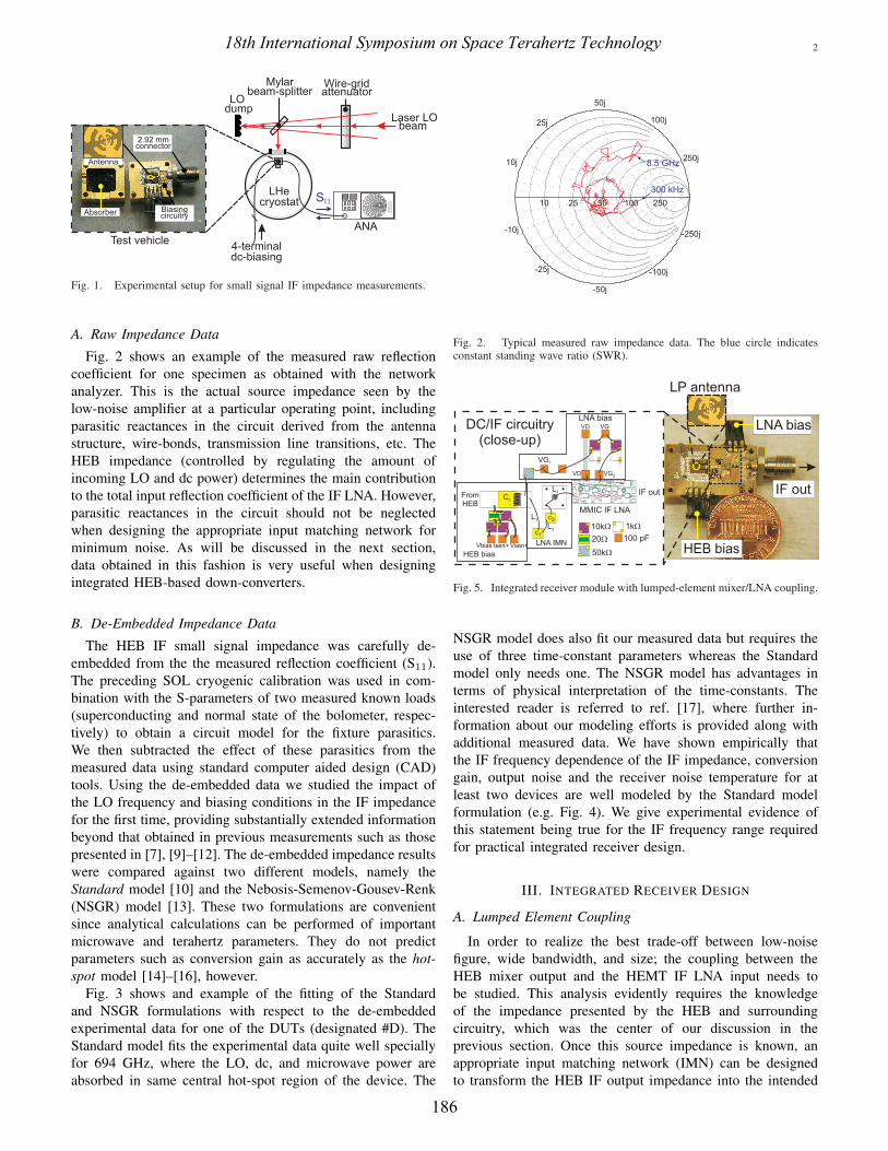
We performed an extensive set of impedance measurementson several mixer devices fabricated from thin NbN film (3.5–4 nm thick1) sputtered on a 350 µm thick silicon substrate.The measurements were completed using an automatic net-work analyzer (ANA). The active NbN area was 0.4–0.5 µmlong by 2 µm wide. We used various LO drive frequenciesranging from 694 GHz up to nearly 2 THz, which coverregions of the electromagnetic spectrum below and abovethe superconducting bandgap frequency of NbN for typicalfilm parameters. The local oscillator source is the same CO2-pumped far infrared laser system used in previous studies [8],[9]. The HEBs were quasi-optically coupled using monolithiclog-periodic antennas in combination with a 4 mm diameterelliptical lens made of silicon. This antenna/lens configurationwas designed to operate from 250 GHz to 3 THz. TheIF frequency range covered by the ANA was 300 kHz to8.5 GHz. This frequency range is sufficient to characterize thetypical IF bandwidth for all phonon-cooled NbN HEB mixersdeveloped to date. The measurements required an initial one-port short-open-load (SOL) calibration inside the cryostat. Thecalibration was done by putting each of the standards intothe dewar in three consecutive thermal cycles and measuringthe corresponding S11 using the network analyzer. The powerlevel from the network analyzer was -50 dBm. We designeda customized test vehicle to mount the devices under test(DUTs). This fixture provides the required biasing signalsthrough a broadband resistor network constructed from quartzwire-bondable components. Fig. 1 shows an illustration of theexperimental setup used for these measurements, including apicture of the broadband test fixture.
1The nominal thickness of the NbN film was given by the manufacturer(Moscow State Pedagogical University, MSPU) as 3.5 to 4 nm. Recent TEMmeasurements have yielded a thickness of 5–6 nm for similar films [7].
18th International Symposium on Space Terahertz Technology
185
2
Fig. 1. Experimental setup for small signal IF impedance measurements.
A. Raw Impedance Data
Fig. 2 shows an example of the measured raw reflectioncoefficient for one specimen as obtained with the networkanalyzer. This is the actual source impedance seen by thelow-noise amplifier at a particular operating point, includingparasitic reactances in the circuit derived from the antennastructure, wire-bonds, transmission line transitions, etc. TheHEB impedance (controlled by regulating the amount ofincoming LO and dc power) determines the main contributionto the total input reflection coefficient of the IF LNA. However,parasitic reactances in the circuit should not be neglectedwhen designing the appropriate input matching network forminimum noise. As will be discussed in the next section,data obtained in this fashion is very useful when designingintegrated HEB-based down-converters.
B. De-Embedded Impedance Data
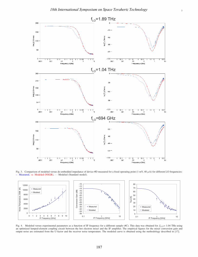
The HEB IF small signal impedance was carefully de-embedded from the the measured reflection coefficient (S11).The preceding SOL cryogenic calibration was used in com-bination with the S-parameters of two measured known loads(superconducting and normal state of the bolometer, respec-tively) to obtain a circuit model for the fixture parasitics.We then subtracted the effect of these parasitics from themeasured data using standard computer aided design (CAD)tools. Using the de-embedded data we studied the impact ofthe LO frequency and biasing conditions in the IF impedancefor the first time, providing substantially extended informationbeyond that obtained in previous measurements such as thosepresented in [7], [9]–[12]. The de-embedded impedance resultswere compared against two different models, namely theStandard model [10] and the Nebosis-Semenov-Gousev-Renk(NSGR) model [13]. These two formulations are convenientsince analytical calculations can be performed of importantmicrowave and terahertz parameters. They do not predictparameters such as conversion gain as accurately as the hot-spot model [14]–[16], however.
Fig. 3 shows and example of the fitting of the Standardand NSGR formulations with respect to the de-embeddedexperimental data for one of the DUTs (designated #D). TheStandard model fits the experimental data quite well speciallyfor 694 GHz, where the LO, dc, and microwave power areabsorbed in same central hot-spot region of the device. The
Fig. 2. Typical measured raw impedance data. The blue circle indicatesconstant standing wave ratio (SWR).
Fig. 5. Integrated receiver module with lumped-element mixer/LNA coupling.
NSGR model does also fit our measured data but requires theuse of three time-constant parameters whereas the Standardmodel only needs one. The NSGR model has advantages interms of physical interpretation of the time-constants. Theinterested reader is referred to ref. [17], where further in-formation about our modeling efforts is provided along withadditional measured data. We have shown empirically thatthe IF frequency dependence of the IF impedance, conversiongain, output noise and the receiver noise temperature for atleast two devices are well modeled by the Standard modelformulation (e.g. Fig. 4). We give experimental evidence ofthis statement being true for the IF frequency range requiredfor practical integrated receiver design.
III. INTEGRATED RECEIVER DESIGN
A. Lumped Element Coupling
In order to realize the best trade-off between low-noisefigure, wide bandwidth, and size; the coupling between theHEB mixer output and the HEMT IF LNA input needs tobe studied. This analysis evidently requires the knowledgeof the impedance presented by the HEB and surroundingcircuitry, which was the center of our discussion in theprevious section. Once this source impedance is known, anappropriate input matching network (IMN) can be designedto transform the HEB IF output impedance into the intended
18th International Symposium on Space Terahertz Technology
186
3
Fig. 3. Comparison of modeled versus de-embedded impedance of device #D measured for a fixed operating point (1 mV, 40 µA) for different LO frequencies:– Measured, -x- Modeled (NSGR), - - Modeled (Standard model).
Fig. 4. Modeled versus experimental parameters as a function of IF frequency for a different sample (#C). This data was obtained for fLO= 1.04 THz usingan optimized lumped-element coupling circuit between the hot electron mixer and the IF amplifier. The empirical figures for the mixer conversion gain andoutput noise are estimated from the U-factor and the receiver noise temperature. The modeled curve is obtained using the methodology described in [17].
18th International Symposium on Space Terahertz Technology
187
4
TABLE IPERFORMANCE OF TWO MIXER SAMPLES MEASURED USING THE
optimum source impedance Zopt required by the LNA.
Since the input impedance of a HEMT-based amplifier ismainly dominated by the gate-to-source capacitive reactanceof the first transistor stage, the IMN should behave as aseries inductor. One such IMN has already been successfullyimplemented by our group in the form of a multi-sectionmicrostrip transformer [18]. The use of a lumped-elementmatching network with wire-bonds as inductive elementsto further reduce the down-converter size was proposed inprevious editions of the ISSTT proceedings [8], [9]. Asshown in Fig. 5, we have recently been able to successfullyimplement such a coupling circuit. The design methodologyemployed as well as the measured performance of this receiverimplementation are discussed in great detail in [17]. In theproposed design methodology, we used the Standard modelformulation for the mixer with parameters extracted from theimpedance measurements, in combination with CAD modelsfor the IF and dc circuitry to find theoretical estimates of thedown-converter performance (e.g. Fig. 4). The estimations areself-consistent in the sense that they account for the noiseproduced by an MMIC LNA when an HEB is connected at itsinput, including fixture parasitics. Fig. 6 shows the variationof the double sideband receiver noise temperature, TR,DSB,as a function of IF frequency for two different operatingpoints measured on sample #D. The biasing points were theoptimum (1.5 mV, 35 µA) and (1.0 mV, 35 µA) using an LOfrequency of 694 GHz. This plot shows a remarkable noisebandwidth of 8 GHz for the lowest-noise quiescent point. Thenarrower bandwidth observed at a slightly lower operatingvoltage agrees with the expected lower electron temperature,θ, caused by a lower dc-power dissipated at bias point 2.We have also measured TR,DSB for other LO frequencies(1.04 THz, 1.89 THz, and 2.5 THz) and other devices installedon the same down-converter block. As shown in Table I2, thedemonstrated noise and bandwidth3 figures obtained are verycompetitive, in agreement with theoretical predictions.
2A different mixer sample (designated #C) was used for this comparativeassessment.
3The receiver bandwidth performance was quantified in terms of the IFnoise bandwidth, BN, and the effective IF bandwidth, Beff . BN is thefrequency at which TR,DSB increases by a factor of two with respect toits lowest frequency value. Beff , is the bandwidth of an ideal receiver withperfectly sharp passband that yields the same output noise as the system beingcharacterized [18].
Fig. 6. Double-sideband receiver noise temperature measured atfLO= 0.694 THz (sample #D) for two different bias points: i) 1.5 mV, 35 µA,and ii) 1.0 mV, 35 µA.
B. Three-Dimensional Integration
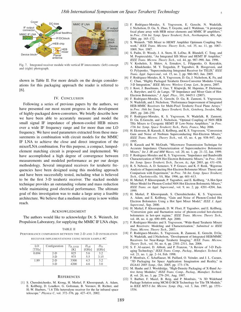
We have mentioned that efficient receiver packaging tech-niques are essential to the development of close-fitting arrays.By far, the most efficient packaging scheme developed to dateis three-dimensional integration. The benefits of 3-D packinghave been thoroughly described in the literature (e.g. [19],[20]). We have recently explored the use of such techniquesto realize an ultra-compact module with an HEB mixer andits corresponding IF amplifier stacked across the z-direction.A straightforward vertical microwave transition has been de-veloped to convey dc and IF signals from the HEB mixerchip to the IF/DC circuitry, both of which are located ondifferent planes. The transition provides impedance matchedcoupling between the coplanar waveguide (CPW) structureon the HEB chip and the microstrip-based MMIC IF LNA.The three-terminal vertical transition was designed based onideas proposed within the electronic packaging community(e.g. [20]–[22]). We used full wave electromagnetic CADtools (CST Microwave Studio) to simulate and optimize theperformance of the IF/DC interconnect. The concept of thepackaged down-converter is illustrated on the left inset ofFig. 7. Aside from the vertical feedthrough itself, the packageconsists of three multi-level blocks:• The device block, where the quasi-optically coupled HEB
mixer chip is mounted.• The IF/DC block, where all the IF circuitry (MMIC
IF LNA included) as well as dc-biasing networks andconnectors are installed.
• The top lid, which is used to provide environmental,mechanical, and electromagnetic shielding for the com-ponents inside the package.
A photograph of the assembled module without cover isshown in the right inset of Fig. 7. The stacked moduletechnique provides a volume reduction of 20 times with acorresponding mass reduction of 15x. The wide bandwidthperformance is preserved at the expense of slightly lower sen-sitivity in this prototype version. A comparison of performancebetween the 2–D and 3–D down-converter implementations is
18th International Symposium on Space Terahertz Technology
188
5
Fig. 7. Integrated receiver module with vertical IF interconnets: (left) conceptand (right) photograph.
shown in Table II. For more details on the design consider-ations for this packaging approach the reader is referred to[6].
IV. CONCLUSION
Following a series of previous papers by the authors, wehave presented our most recent progress in the developmentof highly-packaged down-converters. We briefly describe howwe have been able to accurately measure and model thesmall signal IF impedance of phonon-cooled HEB mixersover a wide IF frequency range and for more than one LOfrequency. We have used parameters extracted from these mea-surements in combination with circuit models for the MMICIF LNA to achieve the close and direct integration of themixer/LNA combination. For this purpose, a compact, lumped-element matching circuit is proposed and implemented. Wehave accomplished a high degree of convergence betweenmeasurements and modeled performance as per our designmethodology. Several integrated receivers for terahertz fre-quencies have been designed using this modeling approachand have been successfully tested, including what is believedto be the first 3-D terahertz receiver. The stacked moduletechnique provides an outstanding volume and mass reductionwhile maintaining good electrical performance. The ultimategoal of this investigation was to make a large array a feasiblearchitecture. We believe that a medium size array is now withinreach.
ACKNOWLEDGMENT
The authors would like to acknowledge Dr. S. Weinreb, JetPropulsion Laboratory, for supplying the MMIC IF LNA chips.
TABLE IIPERFORMANCE COMPARISON BETWEEN THE 2-D AND 3-D INTEGRATION
RECEIVER IMPLEMENTATIONS USING MIXER SAMPLE #C
LO Configuration TR,DSB Beff BN
[THz] [K] [GHz] [GHz]0.694 2-D 825 5.6 3.2
3-D 975 5.5 3.151.89 2-D 3300 4.5 3.2
3-D 4200 4.6 3.0
REFERENCES
[1] S. Cherednichenko, M. Kroug, H. Merkel, P. Khosropanah, A. Adam,E. Kollberg, D. Loudkov, G. Goltsman, B. Voronov, H. Richter, andH.-W. Huebers, “1.6 THz heterodyne receiver for the far infrared spacetelescope.” Physica C, vol. 372–376, pp. 427–431, 2002.
[2] F. Rodriguez-Morales, S. Yngvesson, E. Gerecht, N. Wadefalk,J. Nicholson, D. Gu, X. Zhao, T. Goyette, and J. Waldman, “A prototypefocal plane array with HEB mixer elements and MMIC IF amplifiers.”in Proc. 15th Int. Symp. Space Terahertz Tech., Northampton, MA, Apr.2004, pp. 165–172.
[3] S. Weinreb, “SIS Mixer to HEMT Amplifier Optimum Coupling Net-work,” IEEE Trans. Microw. Theory Tech., vol. 35, no. 11, pp. 1067–1069, Nov. 1987.
[4] S. Padin, D. Woody, J. A. Stern, H. LeDuc, R. Blundell, C. Tong, andM. Pospieszalski, “An Integrated SIS Mixer and HEMT IF Amplifier,”IEEE Trans. Microw. Theory Tech., vol. 44, pp. 987–990, Jun. 1996.
[5] V. Koshelets, S. Shitov, A. Ermakov, L. Filippenko, O. Koryukin,A. Khudchenko, M. Y. Torgashin, P. Yagoubov, R. Hoogeveen, andO. Pylypenko, “Superconducting Integrated Receiver for TELIS,” IEEETrans. Appl. Supercond., vol. 15, no. 2, pp. 960–963, Jun. 2005.
[6] F. Rodriguez-Morales, K. S. Yngvesson, D. Gu, J. Nicholson, K. Fu, andC. Chan, “Highly Packaged Terahertz Down-Converter Modules Using3-D Integration,” IEEE Microw. Wireless Comp. Lett., In press, 2007.
[7] J. Kooi, J. Baselmans, J. Gao, T. Klapwijk, M. Hajenius, P. Dieleman,A. Baryshev, and G. de Lange, “IF Impedance and Mixer Gain of Hot-Electron Bolometers,” J. Appl. Phys., 101, 044511 (2007).
[8] F. Rodriguez-Morales, E. Gerecht, D. Gu, R. Zannoni, S. Yngvesson,N. Wadefalk, and J. Nicholson, “Performance Improvement of IntegratedHEB-MMIC Receivers for Multi-Pixel Terahertz Focal Plane Arrays.”in Proc. 16th Int. Symp. Space Terahertz Tech., Goteborg, Sweden, May2005, pp. 246–250.
[9] F. Rodriguez-Morales, K. S. Yngvesson, N. Wadefalk, R. Zannoni,D. Gu, E.Gerecht, and J. Nicholson, “Optimal Coupling of NbN HEBTHz Mixers to Cryogenic HEMT IF Low-Noise Amplifiers.” in Proc.17th Int. Symp. Space Terahertz Tech., Paris, France, May 2006.
[10] H. Ekstroem, B. Karasik, E. Kollberg, and K. S. Yngvesson, “ConversionGain and Noise of Niobium Superconducting Hot-Electron Mixers,”IEEE Trans. Microw. Theory Tech., vol. 43, no. 4, pp. 938–947, Apr.1995.
[11] B. Karasik and W. McGrath, “Microwave Transmission Technique forAccurate Impedance Characterization of Superconductive BolometricMixers,” Int J. IR and MM Waves, vol. 20, no. 1, pp. 21–32, Jan. 1999.
[12] F. Rodriguez-Morales and K. S. Yngvesson, “Impedance and BandwidthCharacterization of NbN Hot Electron Bolometric Mixers,” in Proc. 14thInt. Symp. Space Terahertz Tech., Tucson, Az, Apr. 2003, pp. 431–438.
[13] R. S. Nebosis, A. D. Semenov, Y. P. Gousev, and K. F. Renk, “RigorousAnalysis of Superconducting Hot-Electron Bolometer Mixer: Theory andComparison with Experiment,” in Proc. 7th Int. Symp. Space TerahertzTech., Charlottesville, VA, Mar. 1996, pp. 601–613.
[14] H. Merkel, P. Khosropanah, P. Yagoubov, and E. Kollberg, “A Hot-SpotMixer Model for Phonon-Cooled NbN Hot Electron Bolometric Mixers,”IEEE Trans. on Appl. Supercond., vol. 9, no. 2, pp. 4201–4204, Jun.1999.
[15] H. Merkel, P. Khosropanah, S. Cherednichenko, K. S. Yngvesson,A. Adam, and E. Kollberg, “Gain and Noise of Phonon-Cooled HotElectron Bolometers Using a Hot Spot Mixer Model,” IEEE J. Appl.Supercond., Sep. 2000.
[16] H. Merkel, P. Khosropanah, D. W. Floet, P. Yagoubov, and E. Kollberg,“Conversion gain and fluctuation noise of phonon-cooled hot-electronbolometers in hot-spot regime,” IEEE Trans. Microw. Theory Tech.,vol. 48, no. 4, pp. 690–699, Apr. 2000.
[17] F. Rodriguez-Morales and S. Yngvesson, “Wide-Band Terahertz Mixersand Receivers: Modeling and Characterization,” Submitted to IEEETrans. Microw. Theory Tech., 2007.
[18] F. Rodriguez-Morales, S. Yngvesson, R. Zannoni, E. Gerecht, D.Gu,N. Wadefalk, and J.Nicholson, “Development of Integrated HEB/MMICReceivers for Near-Range Terahertz Imaging,” IEEE Trans. Microw.Theory Tech., vol. 54, no. 6, pp. 2301–2311, Jun. 2006.
[19] S. F. Al-sarawi, D. Abbott, and P. Franzon, “A Review of 3-D Pack-aging Technology,” IEEE Trans. Comp., Packag., Manufact. Technol. B,vol. 21, no. 1, pp. 2–14, Feb. 1998.
[20] P. Monfraix, C. Schaffauser, M. Paillard, O. Veinder, and J. L. Cazaux,“3D Packaging for Space Application: Imagination and Reality,” inEGAAS 2005 Symp., Oct. 2005, pp. 173–176.
[21] M. Hauhe and J. Wooldridge, “High-Density Packaging of X-Band Ac-tive Array Modules,” IEEE Trans. Comp., Packag., Manufact. Technol.B, vol. 20, no. 3, pp. 279–291, Aug. 1997.
[22] T. Barbier, F. Mazel, B. Reig, and P. Monfraix, “A 3D WidebandPackage Solution using MCM-D BCB Technology for Tile TR Module,”in IEEE MTT-S Int. Microw. Symp. Dig., vol. 3, Jun. 1997, pp. 1551–1554.
18th International Symposium on Space Terahertz Technology