Page 1
1
Highly Robust Silver Nanowire Network for Transparent
Electrode
Tze-Bin Song,†,‡,#
You Seung Rim,†,‡,#
Fengmin Liu,†,‡,§
, Brion Bob,†,‡
, Shenglin Ye,†,‡
Yao-
Tsung Hsieh,†,‡
and Yang Yang*,†,‡
†Department of Materials Science and Engineering, University of California, Los Angeles,
Los Angeles, California 90095, United States, ‡California NanoSystems Institute, University
of California Los Angeles, Los Angeles, CA 90095, United States, and, §College of Electronic
Science and Engineering, Jilin Univsersity, 2699 Qianjin Street, Changchun 130012, PR
China
Page 2
2
ABSTRACT
Solution-processed silver nanowire networks are one of the promising candidates to replace a
traditional indium tin oxide as the next generation transparent and flexible electrodes due to
their ease of processing, moderate flexibility, high transparency and low sheet resistance. To
date however, high stability of the nanowire networks remains a major challenge because the
long-term usages of these electrodes are limited by their poor thermal and chemical stabilities.
Existing methods for addressing this challenge mainly focus on protecting the nanowire
network with additional layers that require vacuum processes, which can lead to an increment
in manufacturing cost. Here, we report a straightforward strategy of a sol-gel processing as a
fast and robust way to improve the stabilities of silver nanowires. Comparing with reported
nanoparticles embedded in nanowire networks, better thermal and chemical stabilities are
achieved via sol-gel coating of TiO2 over the silver nanowire networks. The conformal
surface coverage suppressed the surface diffusion of silver atoms and prevented the chemical
corrosion from the environment. These results highlight the important role of the functional
layer to providing better thermal and chemical stabilities along with improved electrical
properties and mechanical robustness. The silver nanowires/TiO2 composite electrodes were
applied as the source and drain electrodes for In2O3 thin-film transistors (TFTs) and the
devices exhibited improved electrical performance annealed at 300°C without the degradation
of the electrodes. These key findings not only demonstrated a general and effective method to
improve the thermal and chemical stabilities of metal nanowire networks but also provided a
basic guideline towards rational design of highly efficient and robust composite electrodes.
KEYWORDS
Transparent electrode, silver nanowire, sol-gel process, stability, thin-film transistor
Page 3
3
INTRODUCTION
Transparent conducting electrode is an essential component for most optoelectronic devices
and tin-doped indium oxide (ITO) and Al-doped zinc oxide (AZO) are commonly chosen for
this layer due to their low resistivity and high transparency in the visible ranges.1 The
manufacture cost of these materials remains high, however, mainly due to the use of vacuum
techniques. Therefore, great efforts have been put into solution-processed conductive metal
oxides due to its potentially low-cost processing,2 but high temperature annealing (> 350°C) is
required to achieve a conductivity compared with the vacuum process.3-5
Recently, solution
processing of nanowire networks have been developed as a substitute technology for
transparent electrodes, such as carbon nanotube (CNT),6,7
silver nanowire (AgNW)8,9
and
copper nanowire (CuNW).10,11
High transparency and low sheet resistance films can be
obtained through low-temperature solution process (<200°C). In particular, AgNW networks
have been attracted attentions as one of promising candidates due to its favorable
transmittance, conductance, and flexibility, as compared with the traditional ITO film.12,13
Poor thermal and chemical stabilities of these metallic nanowires were observed, however,
restricting the capability of post-processing and potential applications. The instabilities of the
metallic nanowire network are mainly caused by the chemical reaction (including oxidation,
sulfurization) and surface diffusion of metal atoms resulting in contact ripening or Rayleigh
effect.14-16
In particular, the ripening at the contacts of the nanowire network causes a
discontinuous network, which results in a decreased lifetime and limits post-processing. Some
approaches on improving the thermal and chemical stabilities of the nanowire network were
proposed using functional protection layers deposited by vacuum techniques such as atomic
layer deposition and sputtering17-19
, which although effective led to increased manufacturing
cost. Nanoparticles coatings were also reported, although the effectiveness may be limited by
the incomplete coverage of the nanoparticles.20-22
Polymer coatings, such as poly(3,4-
ethylenedioxythiophene):poly(styrenesulfonate) (PEDOT:PSS), were reported facing acid
Page 4
4
degradation and limited thermal stability to 210°C for 20 min.23
Reduced graphene oxide and
graphene provided moisture protection on AgNW were reported, however, the complicated
preparation processes are required and thermal stability in air is still under investigation.24,25
Therefore, a fast and robust process to improve the thermal and chemical stabilities of the
nanowire networks while providing better or equivalent electrical, optical and mechanical
properties is needed.
Here, we demonstrated a sol-gel method using titanium dioxide (TiO2) as a highly efficient
protecting layer over the AgNW networks. The sol-gel TiO2 film has found widespread
application in areas such as antireflection coating,26
wear resistant,27
and chemical resistant
coating.28
The sol-gel solution process is inexpensive and easily adaptable for industrial mass
production. The process can be done in atmospheric conditions and the coating properties can
be precisely controlled by tuning the temperature, chemical contents, and molar ratios of the
precursors. Moreover, a variety of methods are available for depositing these coatings, such as
spin-coating, dipping coating, spray coating, and blade coating. We found that by applying
sol-gel TiO2 onto the AgNW network, the composite electrode showed improved electrical
and optical properties, superior performance in thermal stability tests, bending test, chemical
corrosion test and exhibited better adhesion with the substrates. During the thermal stability
test and chemical stability test, nanowire networks were covered by using a nanoparticle
functional layer and bare nanowire networks are examined along with those functionalized by
the sol-gel TiO2 process. The mechanisms of the stability improvements were discussed in the
manuscript. To confirm the feasibility of our process, we employed AgNW-sol-gel TiO2 as
the source and drain (S/D) electrodes for solution-processed indium oxide (In2O3) thin-film
transistors (TFTs) with a bottom-gate structure through the post-annealing process (300°C).
Surprisingly, we found that the electrical performance of In2O3 TFTs was improved without
electrical degradation of S/D electrodes.
Page 5
5
RESULTS AND DISCUSSION
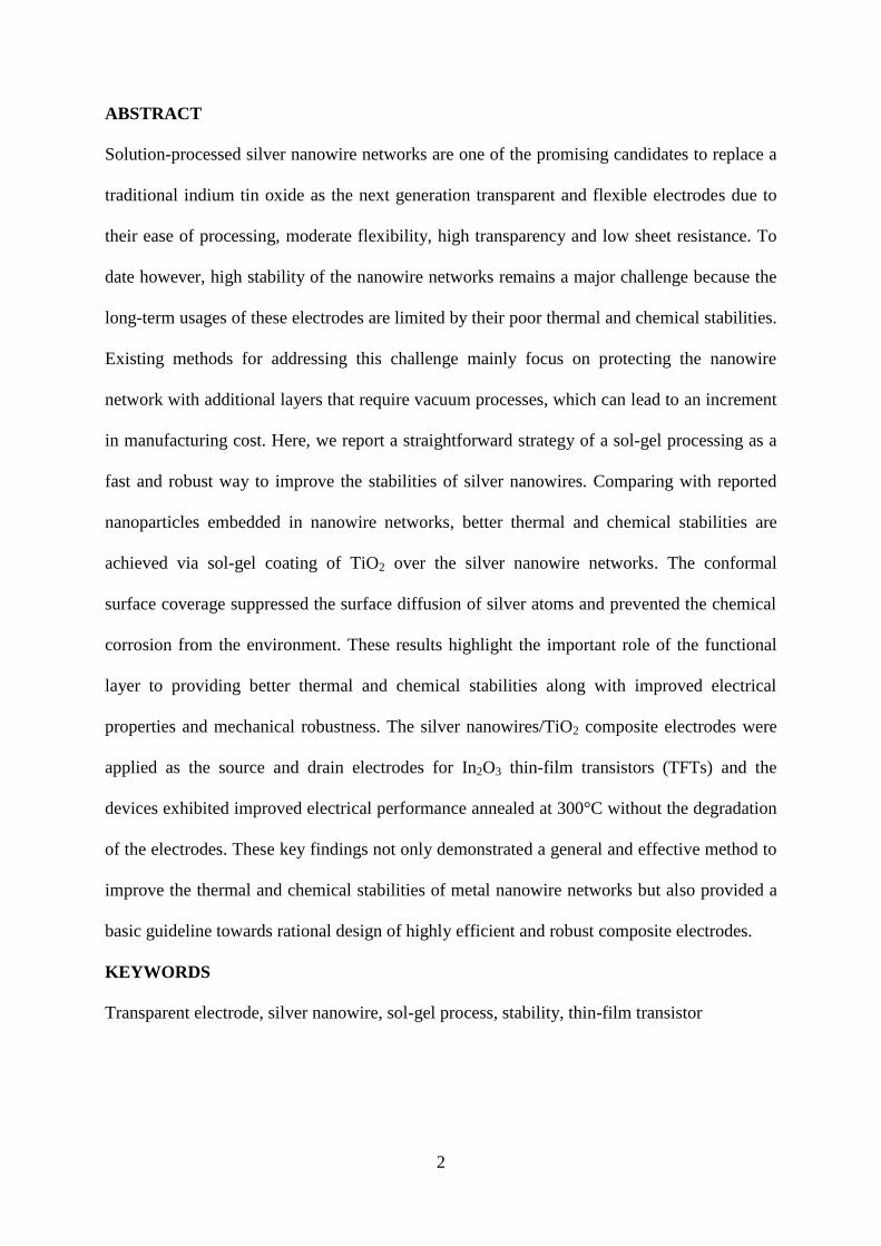
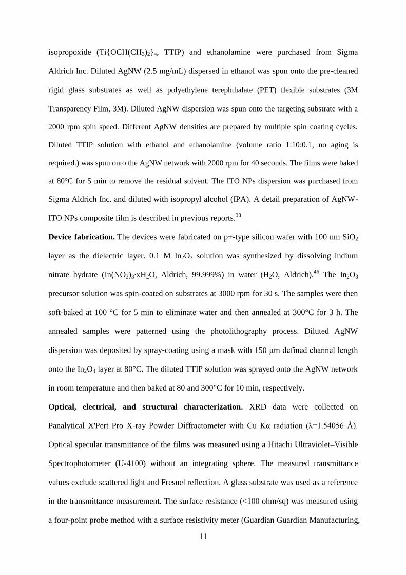
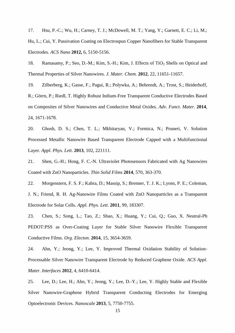
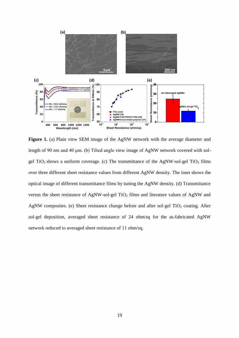
Diluted AgNW dispersion was spun onto the target substrate and the result is shown in the
scanning electron microscopy (SEM) image in Figure 1a. The titanium isopropoxide
(Ti{OCH(CH3)2}4, TTIP) was diluted with ethanol and a small amount of ethanolamine, and
then spun onto the AgNW network. The ethanolamine was added to stabilize the sol
preventing it from forming crystalline precipitations. The AgNW-sol-gel TiO2 composite film
was shown with tilted angle SEM in Figure 1b. The details of the experiment were described
in the experimental section. The sol-gel TiO2 layer exhibited a conformal coverage over the
entire AgNW network with 100~ 150 nm thickness and showed an amorphous phase due to
the room temperature process (X-ray diffraction (XRD) spectra are shown in Figure S1).29
A
thinner layer of sol-gel TiO2 would not provide a full coverage due to the roughness of the
AgNW network. The transmittance and sheet resistance of AgNW-sol-gel TiO2 film are
85.6% at a wavelength of 550 nm and 13.2 ohm/sq, which are superior to the previous report
with a 84% transmittance and a 19 ohm/sq sheet resistance using similar aspect ratio AgNWs
(averaged diameter of 90 nm and averaged length 30 μm), as shown in Figure. 1c and d.16,30,31
Although the transmittance was slightly affected by the sol-gel TiO2 layer, which has a high
transmittance of 99.3% at the wavelength of 550 nm with glass as the reference and an
absorption edge showed at around 340 nm (Figure S2), which corresponding to the
amorphous TiO2.32
It is found that the sheet resistance was significantly reduced after the sol-
gel TiO2 layer deposition even without any heat treatment (Figure 1e). Different with other
processes, including thermal annealing, plasmonic welding and current ripening,16,33-35
the
reduction of the sheet resistance in AgNW-sol-gel TiO2 could be originated from the
shrinking force from the gelation process during the evaporation of the solvent and the
transformation between TTIP and TiO2 network during the drying process, and the increasing
conductive pathways from sol-gel TiO2 coating between adjacent AgNWs.36
Page 6
6
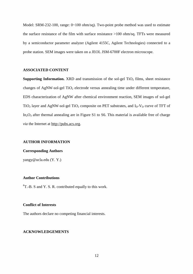
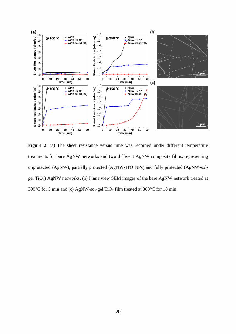
Thermal stability test was done in air under different temperatures with one hour treatment
time, as shown in Figure 2. Bare AgNW networks, AgNW networks incorporated with metal
oxide nanoparticles (NPs) as the functional protecting material were fabricated and tested in
comparison with the sol-gel TiO2 process.21,22,37
The sheet resistance of the as fabricated
AgNW networks was fixed around 20 ohm/sq while extra coatings with nanoparticles and sol-
gel TiO2 would reduce the sheet resistance to around 11 ohm/sq as shown in Figure 1e.38
No
significant changes in the electrical properties was observed for any one of the three cases
during the thermal stability test at 200°C as shown in Figure. 2a. However, when tested at
250°C, the sheet resistance of the bare AgNW film increased rapidly up to values beyond our
measurement capacity of 120 Mohm/sq. When the bare AgNW film was treated at 300°C, the
conductive pathways within the network was disconnected within 5 min as shown in Figure
2b. Some of the nanowires within the bare AgNW network became small droplets due to
contact ripening and Rayleigh instability.39
Meanwhile, the AgNW-sol-gel TiO2 composite
film remained intact after 10 min at 300°C treatment (Figure 2c). For the AgNW-ITO NPs
composite, the ITO NPs provided partial protection to the AgNW network as well as acting as
the conductive matrix to the film. The sheet resistance of AgNW-ITO NPs composite
increased slower than the bare AgNW network, and saturated to around 104 ohm/sq due to the
conductive matrix of ITO NPs under 300°C treatment.40
When the temperature was increased
to 350°C, the sheet resistance of the AgNW-sol-gel TiO2 composite rose gradually to over
120 Mohm/sq in around one hour. Results from higher temperatures (375°C and 400°C) were
shown in Figure S3 and it was clearly shown that the AgNW-sol-gel TiO2 composite
maintained its conductive path and sheet resistance value for more than 5 min under 400°C.
These results demonstrated that the thermal stability of the AgNW network was significantly
improved with the incorporation of sol-gel TiO2. Previously, it has been reported that by
adopting a core-shell AgNW/TiO2 structure, the single AgNW can be stable up to 750°C in 10
min under ultra high vacuum.18
In a nanowire network, however, low surface energy grooves
Page 7
7
are formed at the contacts between wires and these could facilitate the movement of Ag atoms
to the contact through surface and bulk diffusion, causing contact ripening and Rayleigh
effect to happen at a lower temperature or shorter treatment time.16,41
Conformal coating using
sol-gel TiO2 layer over the AgNW network can effectively suppress the surface diffusion and
enhance the thermal stability of the network compared with bare AgNW and NP coated
composite AgNW networks.
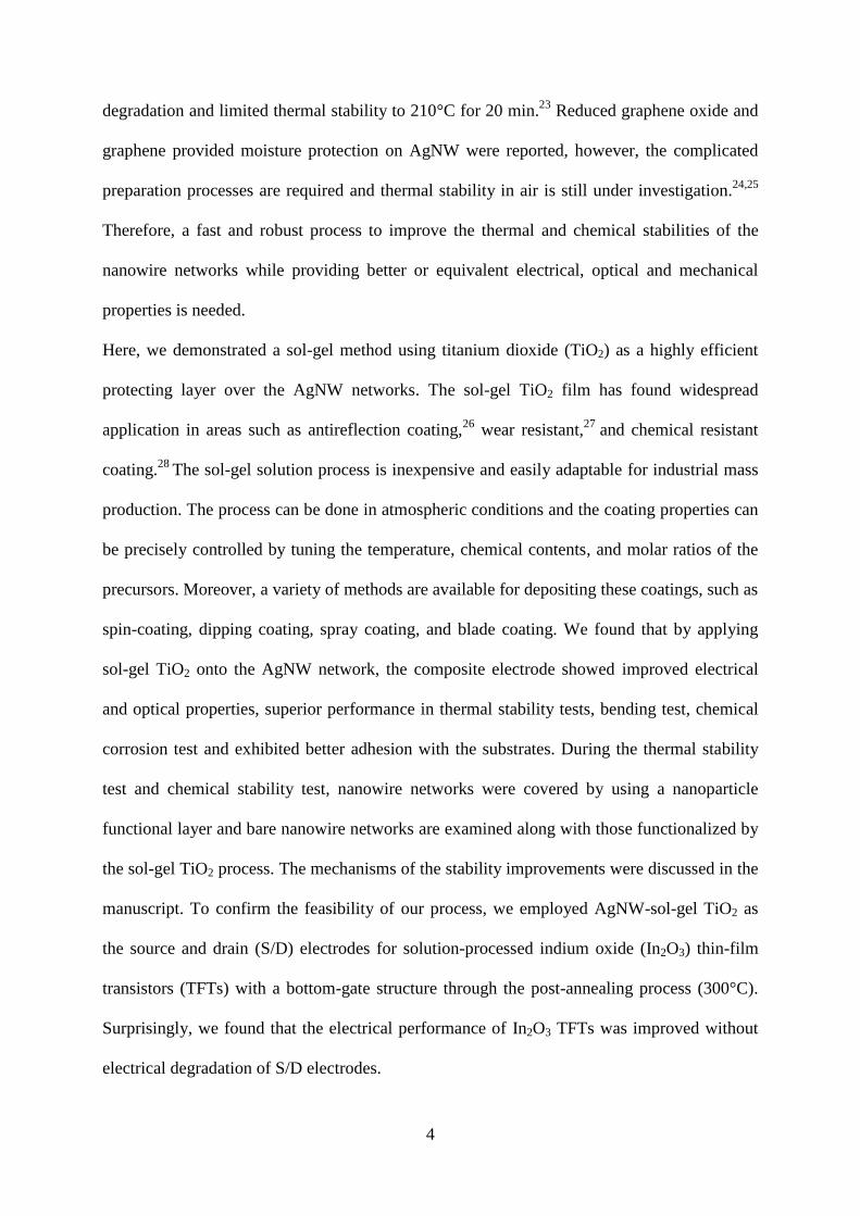
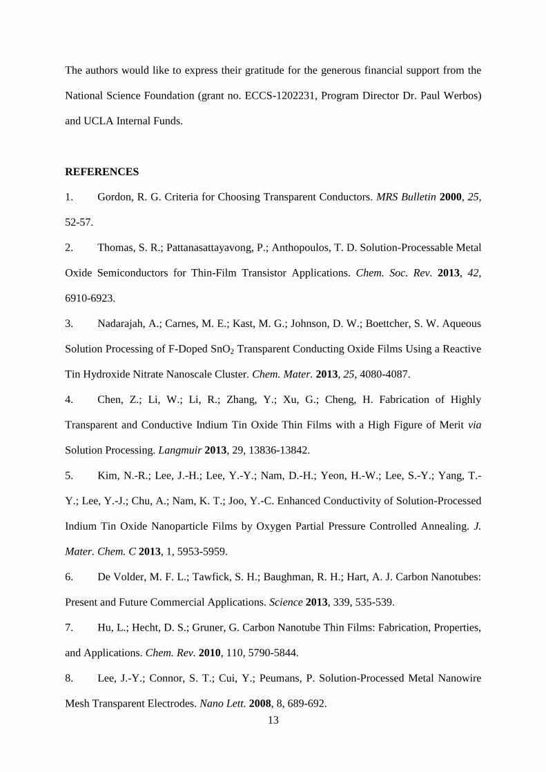
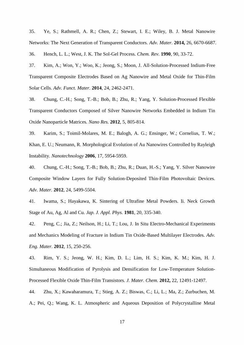
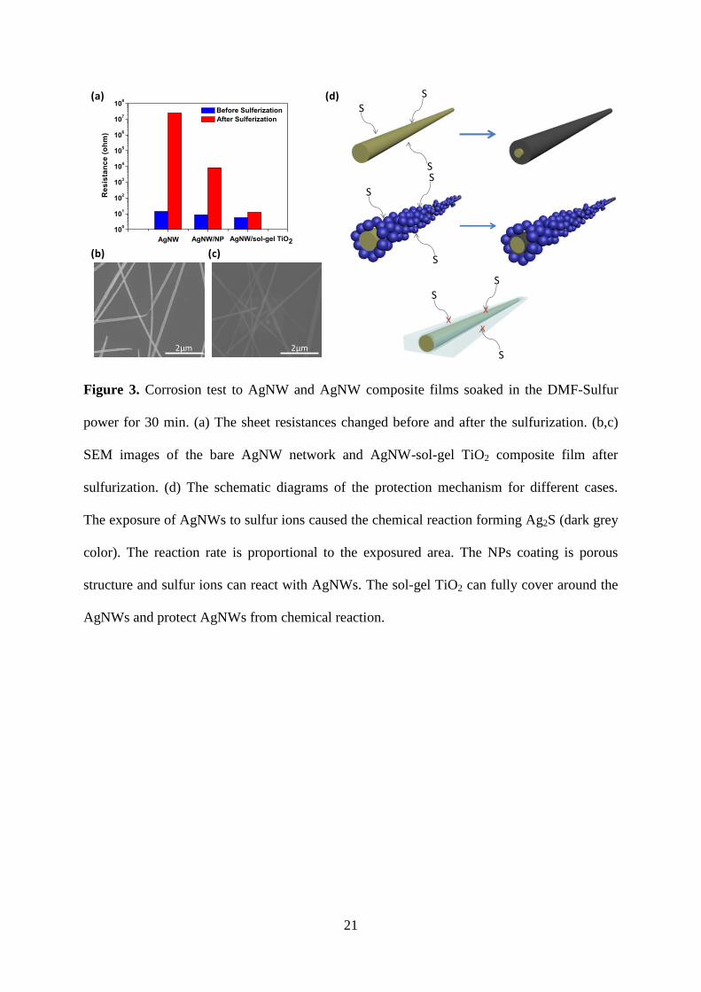
Chemical stability of the AgNW-sol-gel TiO2 composite electrode was examined through
corrosion test comparing these AgNW composite films and bare AgNW network. Although
Ag is stable in most chemical environments; it can be easily reacted with sulfur to form Ag2S,
which is black in color.14
In this case, sulfur was provided dissolved in the solvent
dimethylformamide (DMF) and applied to AgNW network with and without functional
protecting layers. The AgNW films were soaked into 60 ml of DMF solvent containing 0.008
g of sulfur powders for 30 min. Higher chemical stability was observed for the AgNW-sol-gel
TiO2 composite electrode compared with the bare AgNW network and NPs coated AgNW
network, as shown in Figure 3. As shown in Figure 3a, the sheet resistance of the bare AgNW
network increased more than six orders of magnitude of its initial resistance value after the 30
min treatment. The sheet resistance increased around three orders of magnitude for the
AgNW-NPs composite film and the sheet resistance change in both cases could be attributed
to the reaction of Ag with sulfur ion decreasing the amount of the AgNWs present for creating
conductive pathways within the AgNW network. The AgNW-sol-gel TiO2 composite film
was slightly affected and the resistance rose to twice its original value. For the bare AgNW
case, although the AgNWs kept their original shapes but Energy Dispersive X-ray
Spectroscopy (EDS) showed the atomic ratio of silver and sulfur closing to 2:1. This is a clear
indication that most of the AgNWs were corroded by the sulfur ions. Meanwhile, the sol-gel
TiO2 covered AgNW network remained intact as observed by SEM and sulfur was not
detected by EDS analysis, as shown in Figure 3b and c. (EDS results are shown in the Figure
Page 8
8
S4) The three types of AgNW networks investigated behaved differently when placed in a
chemical environment containing sulfur and a schematic diagram was shown in Figure 3d.
The exposed surface area of the AgNWs determines the reaction rate between silver atoms
and sulfur ions, making bare AgNWs most prone to chemical corrosion. NPs in the AgNW-
NPs composite electrode could provide partial protection for the AgNWs, however sulfur ions
could still penetrate the nanoporous structure and react with the Ag atoms, although at a
slower rate compared to the bare AgNW case. The sol-gel layer offered the best corrosion
resistance due to its full coverage of the AgNW network and choosing TiO2 as opposed to
other metal oxides such as zinc oxide can provide the additional benefit of being resistant to
most base and acid solutions, thereby providing a more chemically stable protection.
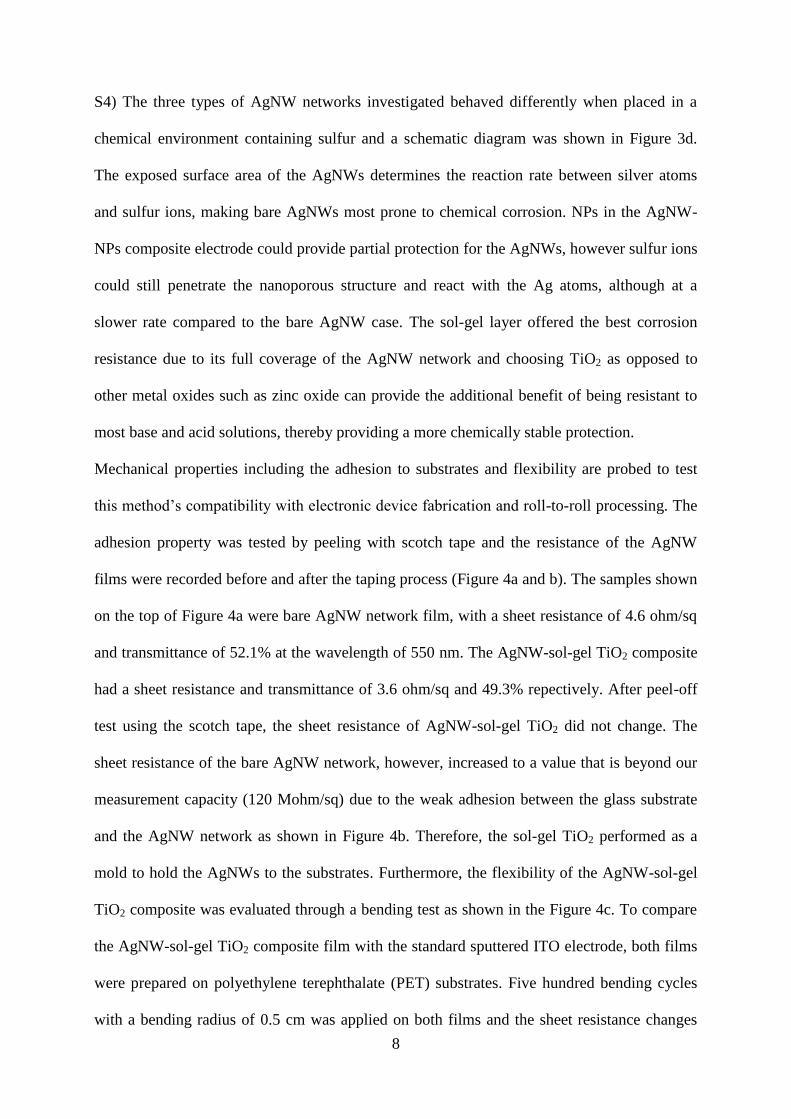
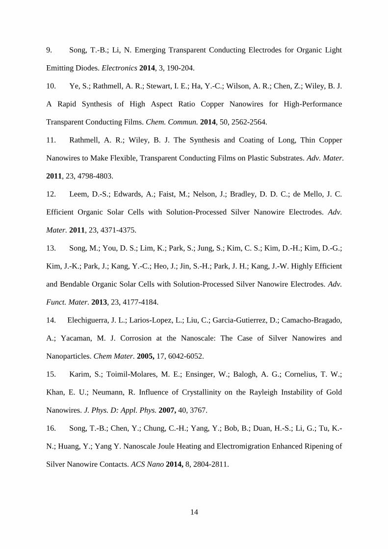
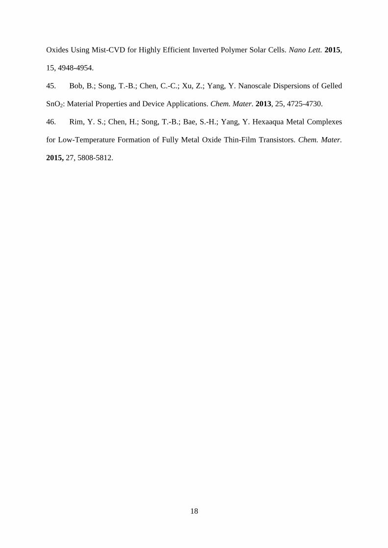
Mechanical properties including the adhesion to substrates and flexibility are probed to test
this method’s compatibility with electronic device fabrication and roll-to-roll processing. The
adhesion property was tested by peeling with scotch tape and the resistance of the AgNW
films were recorded before and after the taping process (Figure 4a and b). The samples shown
on the top of Figure 4a were bare AgNW network film, with a sheet resistance of 4.6 ohm/sq
and transmittance of 52.1% at the wavelength of 550 nm. The AgNW-sol-gel TiO2 composite
had a sheet resistance and transmittance of 3.6 ohm/sq and 49.3% repectively. After peel-off
test using the scotch tape, the sheet resistance of AgNW-sol-gel TiO2 did not change. The
sheet resistance of the bare AgNW network, however, increased to a value that is beyond our
measurement capacity (120 Mohm/sq) due to the weak adhesion between the glass substrate
and the AgNW network as shown in Figure 4b. Therefore, the sol-gel TiO2 performed as a
mold to hold the AgNWs to the substrates. Furthermore, the flexibility of the AgNW-sol-gel
TiO2 composite was evaluated through a bending test as shown in the Figure 4c. To compare
the AgNW-sol-gel TiO2 composite film with the standard sputtered ITO electrode, both films
were prepared on polyethylene terephthalate (PET) substrates. Five hundred bending cycles
with a bending radius of 0.5 cm was applied on both films and the sheet resistance changes
Page 9
9
were recorded. Though, the interface between sol-gel TiO2 and PET substrate is not favorable
and the cracks before bending test were observed under the SEM as in Figure S5. The sheet
resistance of the AgNW-sol-gel TiO2 composite film was still maintained after 500 cycles due
to the conductive path of AgNW networks. On the other hand, the sheet resistance of the
sputtered ITO rapidly increased for even below 100 cycles due to crack formation reducing
the conductive path within the ITO film.42
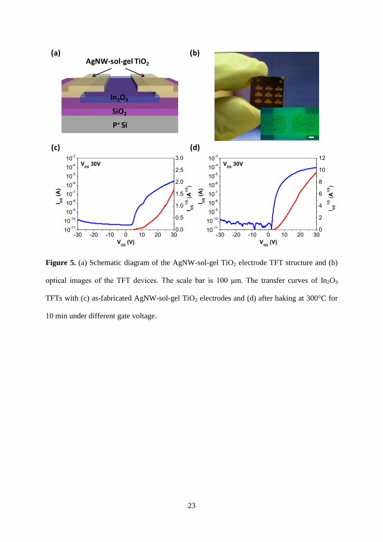
The AgNW-sol-gel TiO2 composite was incorporated into TFT devices as the S/D electrodes
to explore its feasibility as a practical electrode. Solution-processed In2O3 channel material
was formed onto the p+ doped Si wafer with a thermally grown SiO2 (100 nm), and S/D
electrodes were deposited by spray-coating diluted AgNWs and TTIP precursor solutions
through shadow masks on top of the In2O3 layer. A schematic structure of the device is shown
in Figure 5a. A photo of the TFTs was shown in Figure 5b with the inset showing an optical
image of one of the device and the channel length and width were measured to be 90 μm and
820 μm, respectively. Transfer curves of In2O3 TFTs with before and after thermal treatment
were plotted in Figure 5c, and d. As-deposited AgNW-sol-gel TiO2 electrodes-based In2O3
TFTs showed a poor electrical contact and a poor electrical performance, and had the
saturation mobility (μsat) and sub-threshold voltage swing (S.S) of 0.24 cm2·V
-1·s
-1 and 1.72
V·dec-1
, respectively. However, the electrical performance of 300°C annealed In2O3 TFTs
with AgNW-sol-gel TiO2 electrodes was significantly improved and the transfer curve
showed a better switching behavior, as shown in Figure 5d and S6, with μsat and S.S of
devices showed 1.91 cm2·V
-1·s
-1 and 0.80 V·dec
-1, respectively. 80°C annealed TiO2 films
could contain large amount of hydroxide groups due to incomplete dehydroxylation of
precursors.43
Thus, TiO2 layer could not contribute to the improved electrical contact to In2O3
channel layer (as shown in Figure S1). After 300°C annealing for 10 min in air, TiO2
precursor could be fully transferred to TiO2 layer. Typically, TiO2 was well known as an n-
type semiconductor, which could contribute to the carrier transport between AgNWs and
Page 10
10
In2O3 contact. Furthermore, we speculated that the contact between annealed AgNWs and
In2O3 was directly improved. Thus, AgNW-sol-gel TiO2 electrodes showed a better
compatibility to TFT application compared with bare AgNW film by improving the thermal
stability and electrode lifetime of the devices. Further modifications of the sol-gel TiO2 layer
to improve the device contacts are anticipated to achieve better device performance.44,45
CONCLUSIONS AND PROSPECTS
Solution-processed AgNW-sol-gel TiO2 composite electrode was demonstrated to reduce the
sheet resistance of the AgNW network while improving the thermal stability under various
temperatures and treatment times over bare AgNW electrodes by suppressing the surface
diffusion of silver atoms during the thermal treatment. Sol-gel TiO2 were also shown to
provide excellent chemical corrosion resistance for the AgNW network preventing the
sulfurization of silver atoms. Both the thermal stability and chemical stability enhancement
highlighted the superior performance of a full coverage layer, compared to bare AgNW
networks and AgNW-NPs composite electrode with the NPs forming a nanoporous protection
layer. Better thermal and chemical stabilities opened up new possibilities for post-fabrications
with high temperatures or harsh chemical conditions. This was demonstrated by applying
AgNW-sol-gel TiO2 composite electrode as the electrode of TFT devices, in which post
fabrication annealing successfully improved the observed device performance. Moreover, the
sol-gel TiO2 layer could greatly improved AgNW's adhesion to the substrate and the
composite electrodes showed excellent flexibility, making it a promising candidate for
flexible electronics.
EXPERIMENTAL METHODS
AgNW composite film preparation. AgNWs were obtained from Blue Nano Inc with an
averaged diameter of around 90 nm and an averaged length of around 30 μm. Titanium
Page 11
11
isopropoxide (Ti{OCH(CH3)2}4, TTIP) and ethanolamine were purchased from Sigma
Aldrich Inc. Diluted AgNW (2.5 mg/mL) dispersed in ethanol was spun onto the pre-cleaned
rigid glass substrates as well as polyethylene terephthalate (PET) flexible substrates (3M
Transparency Film, 3M). Diluted AgNW dispersion was spun onto the targeting substrate with a
2000 rpm spin speed. Different AgNW densities are prepared by multiple spin coating cycles.
Diluted TTIP solution with ethanol and ethanolamine (volume ratio 1:10:0.1, no aging is
required.) was spun onto the AgNW network with 2000 rpm for 40 seconds. The films were baked
at 80°C for 5 min to remove the residual solvent. The ITO NPs dispersion was purchased from
Sigma Aldrich Inc. and diluted with isopropyl alcohol (IPA). A detail preparation of AgNW-
ITO NPs composite film is described in previous reports.38
Device fabrication. The devices were fabricated on p+-type silicon wafer with 100 nm SiO2
layer as the dielectric layer. 0.1 M In2O3 solution was synthesized by dissolving indium
nitrate hydrate (In(NO3)3∙xH2O, Aldrich, 99.999%) in water (H2O, Aldrich).46
The In2O3
precursor solution was spin-coated on substrates at 3000 rpm for 30 s. The samples were then
soft-baked at 100 °C for 5 min to eliminate water and then annealed at 300°C for 3 h. The
annealed samples were patterned using the photolithography process. Diluted AgNW
dispersion was deposited by spray-coating using a mask with 150 μm defined channel length
onto the In2O3 layer at 80°C. The diluted TTIP solution was sprayed onto the AgNW network
in room temperature and then baked at 80 and 300°C for 10 min, respectively.
Optical, electrical, and structural characterization. XRD data were collected on
Panalytical X'Pert Pro X-ray Powder Diffractometer with Cu Kα radiation (λ=1.54056 Å).
Optical specular transmittance of the films was measured using a Hitachi Ultraviolet–Visible
Spectrophotometer (U-4100) without an integrating sphere. The measured transmittance
values exclude scattered light and Fresnel reflection. A glass substrate was used as a reference
in the transmittance measurement. The surface resistance (<100 ohm/sq) was measured using
a four-point probe method with a surface resistivity meter (Guardian Guardian Manufacturing,
Page 12
12
Model: SRM-232-100, range: 0~100 ohm/sq). Two-point probe method was used to estimate
the surface resistance of the film with surface resistance >100 ohm/sq. TFTs were measured
by a semiconductor parameter analyzer (Agilent 4155C, Agilent Technologies) connected to a
probe station. SEM images were taken on a JEOL JSM-6700F electron microscope.
ASSOCIATED CONTENT
Supporting Information. XRD and transmission of the sol-gel TiO2 films, sheet resistance
changes of AgNW-sol-gel TiO2 electrode versus annealing time under different temperature,
EDS characterization of AgNW after chemical environment reaction, SEM images of sol-gel
TiO2 layer and AgNW-sol-gel TiO2 composite on PET substrates, and ID-VD curve of TFT of
In2O3 after thermal annealing are in Figure S1 to S6. This material is available free of charge
via the Internet at http://pubs.acs.org.
AUTHOR INFORMATION
Corresponding Authors
[email protected] (Y. Y.)
Author Contributions
#T.-B. S and Y. S. R. contributed equally to this work.
Conflict of Interests
The authors declare no competing financial interests.
ACKNOWLEDGEMENTS
Page 13
13
The authors would like to express their gratitude for the generous financial support from the
National Science Foundation (grant no. ECCS-1202231, Program Director Dr. Paul Werbos)
and UCLA Internal Funds.
REFERENCES
1. Gordon, R. G. Criteria for Choosing Transparent Conductors. MRS Bulletin 2000, 25,
52-57.
2. Thomas, S. R.; Pattanasattayavong, P.; Anthopoulos, T. D. Solution-Processable Metal
Oxide Semiconductors for Thin-Film Transistor Applications. Chem. Soc. Rev. 2013, 42,
6910-6923.
3. Nadarajah, A.; Carnes, M. E.; Kast, M. G.; Johnson, D. W.; Boettcher, S. W. Aqueous
Solution Processing of F-Doped SnO2 Transparent Conducting Oxide Films Using a Reactive
Tin Hydroxide Nitrate Nanoscale Cluster. Chem. Mater. 2013, 25, 4080-4087.
4. Chen, Z.; Li, W.; Li, R.; Zhang, Y.; Xu, G.; Cheng, H. Fabrication of Highly
Transparent and Conductive Indium Tin Oxide Thin Films with a High Figure of Merit via
Solution Processing. Langmuir 2013, 29, 13836-13842.
5. Kim, N.-R.; Lee, J.-H.; Lee, Y.-Y.; Nam, D.-H.; Yeon, H.-W.; Lee, S.-Y.; Yang, T.-
Y.; Lee, Y.-J.; Chu, A.; Nam, K. T.; Joo, Y.-C. Enhanced Conductivity of Solution-Processed
Indium Tin Oxide Nanoparticle Films by Oxygen Partial Pressure Controlled Annealing. J.
Mater. Chem. C 2013, 1, 5953-5959.
6. De Volder, M. F. L.; Tawfick, S. H.; Baughman, R. H.; Hart, A. J. Carbon Nanotubes:
Present and Future Commercial Applications. Science 2013, 339, 535-539.
7. Hu, L.; Hecht, D. S.; Gruner, G. Carbon Nanotube Thin Films: Fabrication, Properties,
and Applications. Chem. Rev. 2010, 110, 5790-5844.
8. Lee, J.-Y.; Connor, S. T.; Cui, Y.; Peumans, P. Solution-Processed Metal Nanowire
Mesh Transparent Electrodes. Nano Lett. 2008, 8, 689-692.
Page 14
14
9. Song, T.-B.; Li, N. Emerging Transparent Conducting Electrodes for Organic Light
Emitting Diodes. Electronics 2014, 3, 190-204.
10. Ye, S.; Rathmell, A. R.; Stewart, I. E.; Ha, Y.-C.; Wilson, A. R.; Chen, Z.; Wiley, B. J.
A Rapid Synthesis of High Aspect Ratio Copper Nanowires for High-Performance
Transparent Conducting Films. Chem. Commun. 2014, 50, 2562-2564.
11. Rathmell, A. R.; Wiley, B. J. The Synthesis and Coating of Long, Thin Copper
Nanowires to Make Flexible, Transparent Conducting Films on Plastic Substrates. Adv. Mater.
2011, 23, 4798-4803.
12. Leem, D.-S.; Edwards, A.; Faist, M.; Nelson, J.; Bradley, D. D. C.; de Mello, J. C.
Efficient Organic Solar Cells with Solution-Processed Silver Nanowire Electrodes. Adv.
Mater. 2011, 23, 4371-4375.
13. Song, M.; You, D. S.; Lim, K.; Park, S.; Jung, S.; Kim, C. S.; Kim, D.-H.; Kim, D.-G.;
Kim, J.-K.; Park, J.; Kang, Y.-C.; Heo, J.; Jin, S.-H.; Park, J. H.; Kang, J.-W. Highly Efficient
and Bendable Organic Solar Cells with Solution-Processed Silver Nanowire Electrodes. Adv.
Funct. Mater. 2013, 23, 4177-4184.
14. Elechiguerra, J. L.; Larios-Lopez, L.; Liu, C.; Garcia-Gutierrez, D.; Camacho-Bragado,
A.; Yacaman, M. J. Corrosion at the Nanoscale: The Case of Silver Nanowires and
Nanoparticles. Chem Mater. 2005, 17, 6042-6052.
15. Karim, S.; Toimil-Molares, M. E.; Ensinger, W.; Balogh, A. G.; Cornelius, T. W.;
Khan, E. U.; Neumann, R. Influence of Crystallinity on the Rayleigh Instability of Gold
Nanowires. J. Phys. D: Appl. Phys. 2007, 40, 3767.
16. Song, T.-B.; Chen, Y.; Chung, C.-H.; Yang, Y.; Bob, B.; Duan, H.-S.; Li, G.; Tu, K.-
N.; Huang, Y.; Yang Y. Nanoscale Joule Heating and Electromigration Enhanced Ripening of
Silver Nanowire Contacts. ACS Nano 2014, 8, 2804-2811.
Page 15
15
17. Hsu, P.-C.; Wu, H.; Carney, T. J.; McDowell, M. T.; Yang, Y.; Garnett, E. C.; Li, M.;
Hu, L.; Cui, Y. Passivation Coating on Electrospun Copper Nanofibers for Stable Transparent
Electrodes. ACS Nano 2012, 6, 5150-5156.
18. Ramasamy, P.; Seo, D.-M.; Kim, S.-H.; Kim, J. Effects of TiO2 Shells on Optical and
Thermal Properties of Silver Nanowires. J. Mater. Chem. 2012, 22, 11651-11657.
19. Zilberberg, K.; Gasse, F.; Pagui, R.; Polywka, A.; Behrendt, A.; Trost, S.; Heiderhoff,
R.; Görrn, P.; Riedl, T. Highly Robust Indium-Free Transparent Conductive Electrodes Based
on Composites of Silver Nanowires and Conductive Metal Oxides. Adv. Funct. Mater. 2014,
24, 1671-1678.
20. Ghosh, D. S.; Chen, T. L.; Mkhitaryan, V.; Formica, N.; Pruneri, V. Solution
Processed Metallic Nanowire Based Transparent Electrode Capped with a Multifunctional
Layer. Appl. Phys. Lett. 2013, 102, 221111.
21. Shen, G.-H.; Hong, F. C.-N. Ultraviolet Photosensors Fabricated with Ag Nanowires
Coated with ZnO Nanoparticles. Thin Solid Films 2014, 570, 363-370.
22. Morgenstern, F. S. F.; Kabra, D.; Massip, S.; Brenner, T. J. K.; Lyons, P. E.; Coleman,
J. N.; Friend, R. H. Ag-Nanowire Films Coated with ZnO Nanoparticles as a Transparent
Electrode for Solar Cells. Appl. Phys. Lett. 2011, 99, 183307.
23. Chen, S.; Song, L.; Tao, Z.; Shao, X.; Huang, Y.; Cui, Q.; Guo, X. Neutral-Ph
PEDOT:PSS as Over-Coating Layer for Stable Silver Nanowire Flexible Transparent
Conductive Films. Org. Electon. 2014, 15, 3654-3659.
24. Ahn, Y.; Jeong, Y.; Lee, Y. Improved Thermal Oxidation Stability of Solution-
Processable Silver Nanowire Transparent Electrode by Reduced Graphene Oxide. ACS Appl.
Mater. Interfaces 2012, 4, 6410-6414.
25. Lee, D.; Lee, H.; Ahn, Y.; Jeong, Y.; Lee, D.-Y.; Lee, Y. Highly Stable and Flexible
Silver Nanowire-Graphene Hybrid Transparent Conducting Electrodes for Emerging
Optoelectronic Devices. Nanoscale 2013, 5, 7750-7755.
Page 16
16
26. Langlet, M.; Burgos, M.; Coutier, C.; Jimenez, C.; Morant, C.; Manso, M. Low
Temperature Preparation of High Refractive Index and Mechanically Resistant Sol-Gel TiO2
Films for Multilayer Antireflective Coating Applications. J. Sol-Gel Sci. Tech. 2001, 22, 139-
150.
27. Szalkowska, E.; Gluszek, J.; Masalski, J.; Tylus, W. Structure and Protective
Properties of TiO2 Coatings Obtained Using the Sol-Gel Technique. J. Mater. Sci. Lett. 2001,
20, 495-497.
28. Lima Neto, P.; Atik, M.; Avaca, L.; Aegerter, M. Sol-Gel Coatings for Chemical
Protection of Stainless Steel. J. Sol-Gel Sci. Tech. 1994, 2, 529-534.
29. La Notte, L.; Salamandra, L.; Zampetti, A.; Brunetti, F.; Brown, T. M.; Di Carlo, A.;
Reale, A. Airbrush Spray Coating of Amorphous Titanium Dioxide for Inverted Polymer
Solar Cells. Int. J. Photoenergy 2012, 2012, 1-5.
30. Zhu, R.; Chung, C.-H.; Cha, K. C.; Yang, W.; Zheng, Y. B.; Zhou, H.; Song, T.-B.;
Chen, C.-C.; Weiss, P. S.; Li, G.; Yang, Y. Fused Silver Nanowires with Metal Oxide
Nanoparticles and Organic Polymers for Highly Transparent Conductors. ACS Nano 2011, 5,
9877-9882.
31. Yu, Z.; Li, L.; Zhang, Q.; Hu, W.; Pei, Q. Silver Nanowire-Polymer Composite
Electrodes for Efficient Polymer Solar Cells. Adv. Mater. 2011, 23, 4453-44577.
32. Bernardi, M. I. B.; Lee, E. J. H.; Lisboa-Filho, P. N.; Leite, E. R.; Longo, E.; Varela, J.
A. TiO2 Thin Film Growth Using the MOCVD Method. Mater. Res. 2001, 4, 223-226.
33. Garnett, E. C.; Cai, W.; Cha, J. J.; Mahmood, F.; Connor, S. T.; Greyson Christoforo,
M.; Cui, Y.; McGehee, M. D.; Brongersma, M. L. Self-Limited Plasmonic Welding of Silver
Nanowire Junctions. Nature Mater. 2012, 11, 241-249.
34. Hu, L.; Kim, H. S.; Lee, J.-Y.; Peumans, P.; Cui, Y. Scalable Coating and Properties
of Transparent, Flexible, Silver Nanowire Electrodes. ACS Nano 2010, 4, 2955-2963.
Page 17
17
35. Ye, S.; Rathmell, A. R.; Chen, Z.; Stewart, I. E.; Wiley, B. J. Metal Nanowire
Networks: The Next Generation of Transparent Conductors. Adv. Mater. 2014, 26, 6670-6687.
36. Hench, L. L.; West, J. K. The Sol-Gel Process. Chem. Rev. 1990, 90, 33-72.
37. Kim, A.; Won, Y.; Woo, K.; Jeong, S.; Moon, J. All-Solution-Processed Indium-Free
Transparent Composite Electrodes Based on Ag Nanowire and Metal Oxide for Thin-Film
Solar Cells. Adv. Funct. Mater. 2014, 24, 2462-2471.
38. Chung, C.-H.; Song, T.-B.; Bob, B.; Zhu, R.; Yang, Y. Solution-Processed Flexible
Transparent Conductors Composed of Silver Nanowire Networks Embedded in Indium Tin
Oxide Nanoparticle Matrices. Nano Res. 2012, 5, 805-814.
39. Karim, S.; Toimil-Molares, M. E.; Balogh, A. G.; Ensinger, W.; Cornelius, T. W.;
Khan, E. U.; Neumann, R. Morphological Evolution of Au Nanowires Controlled by Rayleigh
Instability. Nanotechnology 2006, 17, 5954-5959.
40. Chung, C.-H.; Song, T.-B.; Bob, B.; Zhu, R.; Duan, H.-S.; Yang, Y. Silver Nanowire
Composite Window Layers for Fully Solution-Deposited Thin-Film Photovoltaic Devices.
Adv. Mater. 2012, 24, 5499-5504.
41. Iwama, S.; Hayakawa, K. Sintering of Ultrafine Metal Powders. Ii. Neck Growth
Stage of Au, Ag, Al and Cu. Jap. J. Appl. Phys. 1981, 20, 335-340.
42. Peng, C.; Jia, Z.; Neilson, H.; Li, T.; Lou, J. In Situ Electro-Mechanical Experiments
and Mechanics Modeling of Fracture in Indium Tin Oxide-Based Multilayer Electrodes. Adv.
Eng. Mater. 2012, 15, 250-256.
43. Rim, Y. S.; Jeong, W. H.; Kim, D. L.; Lim, H. S.; Kim, K. M.; Kim, H. J.
Simultaneous Modification of Pyrolysis and Densification for Low-Temperature Solution-
Processed Flexible Oxide Thin-Film Transistors. J. Mater. Chem. 2012, 22, 12491-12497.
44. Zhu, X.; Kawaharamura, T.; Stieg, A. Z.; Biswas, C.; Li, L.; Ma, Z.; Zurbuchen, M.
A.; Pei, Q.; Wang, K. L. Atmospheric and Aqueous Deposition of Polycrystalline Metal
Page 18
18
Oxides Using Mist-CVD for Highly Efficient Inverted Polymer Solar Cells. Nano Lett. 2015,
15, 4948-4954.
45. Bob, B.; Song, T.-B.; Chen, C.-C.; Xu, Z.; Yang, Y. Nanoscale Dispersions of Gelled
SnO2: Material Properties and Device Applications. Chem. Mater. 2013, 25, 4725-4730.
46. Rim, Y. S.; Chen, H.; Song, T.-B.; Bae, S.-H.; Yang, Y. Hexaaqua Metal Complexes
for Low-Temperature Formation of Fully Metal Oxide Thin-Film Transistors. Chem. Mater.
2015, 27, 5808-5812.
Page 19
19
500 nm5 μm
(a) (b)
0
10
20
30
40
As Fabricated AgNWs
0
10
20
30
40
Sh
ee
t R
es
ista
nc
e (
oh
m/s
q)
AgNWs-sol-gel TiO2
400 600 800 1000 1200 1400
0
20
40
60
80
100
Tra
ns
mit
tan
ce
(%
)
Wavelength (nm)
Rs = 63.2 ohm/sq
Rs = 13.2 ohm/sq
Rs = 7.7 ohm/sq
(e)(c)
100
101
102
103
50
60
70
80
90
100
This work
AgNW [16]
AgNW-TiO2-PEDOT:PSS [30]
AgNW/Cross-linked polymer [31]
Tra
ns
mit
tan
ce
at
55
0n
m (
%)
Sheet Resistance (ohm/sq)
(d)
Figure 1. (a) Plain view SEM image of the AgNW network with the average diameter and
length of 90 nm and 40 μm. (b) Tilted angle view image of AgNW network covered with sol-
gel TiO2 shows a uniform coverage. (c) The transmittance of the AgNW-sol-gel TiO2 films
over three different sheet resistance values from different AgNW density. The inset shows the
optical image of different transmittance films by tuning the AgNW density. (d) Transmittance
versus the sheet resistance of AgNW-sol-gel TiO2 films and literature values of AgNW and
AgNW composites. (e) Sheet resistance change before and after sol-gel TiO2 coating. After
sol-gel deposition, averaged sheet resistance of 24 ohm/sq for the as-fabricated AgNW
network reduced to averaged sheet resistance of 11 ohm/sq.
Page 20
20
0 10 20 30 40 50 60
101
102
103
104
105
106
107
108
Sh
ee
t R
es
ista
nc
e (
oh
m/s
q)
Time (min)
AgNW
AgNW-ITO NP
AgNW-sol-gel TiO2
0 10 20 30 40 50 60
101
102
103
104
105
106
107
108
Sh
ee
t R
es
ista
nc
e (
oh
m/s
q)
Time (min)
AgNW
AgNW-ITO NP
AgNW-sol-gel TiO2
0 10 20 30 40 50 60
101
102
103
104
105
106
107
108
AgNW
AgNW-ITO NP
AgNW-sol-gel TiO2
Sh
ee
t R
es
ista
nc
e (
oh
m/s
q)
Time (min)0 10 20 30 40 50 60
101
102
103
104
105
106
107
108
Sh
ee
t R
es
ista
nc
e (
oh
m/s
q)
Time (min)
AgNW
AgNW-ITO NP
AgNW-sol-gel TiO2
(a) (b)
(c)
3 μm
3 μm
@ 200 °C @ 250 °C
@ 350 °C@ 300 °C
Figure 2. (a) The sheet resistance versus time was recorded under different temperature
treatments for bare AgNW networks and two different AgNW composite films, representing
unprotected (AgNW), partially protected (AgNW-ITO NPs) and fully protected (AgNW-sol-
gel TiO2) AgNW networks. (b) Plane view SEM images of the bare AgNW network treated at
300°C for 5 min and (c) AgNW-sol-gel TiO2 film treated at 300°C for 10 min.
Page 21
21
100
101
102
103
104
105
106
107
108
Before Sulferization
After Sulferization
AgNW/sol-gel TiO2AgNW/NP
AgNW
Re
sis
tan
ce
(o
hm
)
2μm 2μm
(a)
(b) (c)
(d)
xx
x
S
S
SS
S
S
S
S
S
Figure 3. Corrosion test to AgNW and AgNW composite films soaked in the DMF-Sulfur
power for 30 min. (a) The sheet resistances changed before and after the sulfurization. (b,c)
SEM images of the bare AgNW network and AgNW-sol-gel TiO2 composite film after
sulfurization. (d) The schematic diagrams of the protection mechanism for different cases.
The exposure of AgNWs to sulfur ions caused the chemical reaction forming Ag2S (dark grey
color). The reaction rate is proportional to the exposured area. The NPs coating is porous
structure and sulfur ions can react with AgNWs. The sol-gel TiO2 can fully cover around the
AgNWs and protect AgNWs from chemical reaction.
Page 22
22
0 100 200 300 400 500
100
101
102
103
AgNW-sol-gel TiO2
ITO
Rs
(n)/
Rs
(0)
Bending Cycle (number)
(a) (c)
1 cm
Bare AgNW filmRs = 4.6 ohm/sq
T550nm= 52.1%
AgNW-sol-gel TiO2
Rs = 3.6 ohm/sqT550nm= 49.3%
(b)
Figure 4. Photos of bare AgNW (top) films and AgNW-sol-gel TiO2 (bottom) before (a) and
after tape test (b). The high densities of AgNW films were used to have a better contrast of the
images. The sheet resistance of the bare AgNW films was 4.6 ohm/sq and the AgNW-sol-gel
TiO2 was 3.6 ohm/sq. After adhesion test, the AgNW-sol-gel TiO2 remained conductive and
the bare AgNW was peeled from the substrate. The scotch tape was placed on the right hand
side of the samples in (b). (c) Variations in the sheet resistance of AgNW-sol-gel TiO2 and
sputtered ITO film on PET substrates as a function of number of cycles of bending to a 0.5 cm
radius curvature. The sheet resistance values were measured after the substrate was relaxed
back to planar shape.
Page 23
23
(b)
(c) (d)
(a)
-30 -20 -10 0 10 20 3010
-11
10-10
10-9
10-8
10-7
10-6
10-5
10-4
10-3
I DS (
A)
VGS
(V)
VDS
30V
0
2
4
6
8
10
12
I DS
1/2 (
A1
/2)
-30 -20 -10 0 10 20 3010
-11
10-10
10-9
10-8
10-7
10-6
10-5
10-4
10-3
VDS
30V
I DS (
A)
VGS
(V)
0.0
0.5
1.0
1.5
2.0
2.5
3.0
I DS
1/2 (
A1
/2)
P+ Si
SiO2
In2O3
AgNW-sol-gel TiO2
Figure 5. (a) Schematic diagram of the AgNW-sol-gel TiO2 electrode TFT structure and (b)
optical images of the TFT devices. The scale bar is 100 μm. The transfer curves of In2O3
TFTs with (c) as-fabricated AgNW-sol-gel TiO2 electrodes and (d) after baking at 300°C for
10 min under different gate voltage.