University of New Orleans ScholarWorks@UNO University of New Orleans eses and Dissertations Dissertations and eses 12-17-2010 Highly Sensitive and Selective Gas Sensors Based on Vertically Aligned Metal Oxide Nanowire Arrays Jiajun Chen University of New Orleans Follow this and additional works at: hps://scholarworks.uno.edu/td is Dissertation-Restricted is brought to you for free and open access by the Dissertations and eses at ScholarWorks@UNO. It has been accepted for inclusion in University of New Orleans eses and Dissertations by an authorized administrator of ScholarWorks@UNO. e author is solely responsible for ensuring compliance with copyright. For more information, please contact [email protected]. Recommended Citation Chen, Jiajun, "Highly Sensitive and Selective Gas Sensors Based on Vertically Aligned Metal Oxide Nanowire Arrays" (2010). University of New Orleans eses and Dissertations. 106. hps://scholarworks.uno.edu/td/106
Transcript
University of New OrleansScholarWorks@UNO
University of New Orleans Theses and Dissertations Dissertations and Theses
12-17-2010
Highly Sensitive and Selective Gas Sensors Basedon Vertically Aligned Metal Oxide NanowireArraysJiajun ChenUniversity of New Orleans
Follow this and additional works at: https://scholarworks.uno.edu/td
This Dissertation-Restricted is brought to you for free and open access by the Dissertations and Theses at ScholarWorks@UNO. It has been acceptedfor inclusion in University of New Orleans Theses and Dissertations by an authorized administrator of ScholarWorks@UNO. The author is solelyresponsible for ensuring compliance with copyright. For more information, please contact [email protected].
Recommended CitationChen, Jiajun, "Highly Sensitive and Selective Gas Sensors Based on Vertically Aligned Metal Oxide Nanowire Arrays" (2010).University of New Orleans Theses and Dissertations. 106.https://scholarworks.uno.edu/td/106
A Gas Sensor Testing System Used in This Dissertation 91
B Data Extracted from a Responsive Curve of Gas Sensor Testing 93
C Principle Component Analysis 95
D Copyright Permissions 97
References 107
Vita 126
vii
Abstract
Mimicking the biological olfactory systems that consist of olfactory receptor arrays with large
surface area and massively-diversified chemical reactivity, three dimensional (3D) metal oxide
nanowire arrays were used as the active materials for gas detection. Metal oxide nanowire ar-
rays share similar 3D structures as the array of mammal’s olfactory receptors and the chemical
reactivity of nanowire array can be modified by surface coatings. In this dissertation, two stan-
dalone gas sensors based on metal oxide nanowire arrays prepared by microfabrication and in-situ
micromanipulation, respectively, have been demonstrated. The sensors based on WO3 nanowire
arrays can detect 50 ppb NO2 with a fast response; well-aligned CuO nanowire array present a
new detection mechanism, which can identify H2S at a concentration of 500 ppb. To expand the
material library of 3D metal oxide nanowire arrays for gas sensing, a general route to polycrys-
talline metal oxide nanowire array has been introduced by using ZnO nanowire arrays as structural
templates. The effectiveness of this method for high performance gas sensing was first investigated
by single-nanowire devices. The polycrystalline metal oxide coatings showed high performance
for gas detection and their sensitivity can be further enhanced by catalytic noble metal decora-
tions. To form electronic nose systems, different metal oxide coatings and catalytic decorations
were employed to diversify the chemical reactivity of the sensors. The systems can detect low
concentrated H2S and NO2 at room temperature down to part-per-billion level. The system with
different catalytic metal coatings is also capable of discriminiating five different gases (H2S, NO2,
NH3, H2 and CO).
Keywords: Gas Sensors, Nanowires, Nanostructures, Metal Oxides, Three Dimensional
viii
Chapter 1
Introduction
1.1 The Momentum of Nanotechnology
Nanotechnology is a multidisciplinary field, which spans over various basic science and engi-
neering areas. The earliest arise of the term “nano-technology” should be dated back to the year
of 1956, when Prof. Richard Feynman in California Institute of Technology presents the famous
talk “There’s Plenty of Room at the Bottom” [1]. He described the possibility of manipulation of
individual atom or molecule, the new phenomena in the confined scales and the bright future to ex-
pand the functionality of various tools. After that, new discoveries in nanoscale, such as quantum
confinement effect [2], fullerene [3], carbon nanotube [4, 5], and graphene [6], had generated lots
of interest in the nanotechnology. The Clinton’s administration elevated the nanoscience and nano-
technology as a federal level initiative, referred as National Nanotechnology Initiative (NNI) [7], in
2001 when the research in nanotechnology started to pick up its momentum in various disciplines.
Significant advances have been made in the last decade both in fundamental science research and
the applications of nanotechnology. Figure 1.1 gives publication numbers with keyword of “nano-
technology” in last 20 years. The number of related publications have been increase at least 10
times from the year of 2001 to 2009, implying tremendous research efforts have been put into this
area and this trend will be maintained.
There are two major properties of nanomaterials that are employed in many applications of
nanotechnology: quantum confinement effects and large surface-to-volume ratio, which will be
1
Figure 1.1: Number of publications with the keyword “nanotechnology” in last 20 years, acquiredfrom ISIknowledge website.
briefly introduced. As the feature size of nanomaterials reduces to less than 10 nm, the condition of
periodic energy wells in a crystal may be broken down in one or more dimensions and the boundary
effects must be considered. The nanomaterials can be divided into four different categories in terms
of the confinement of dimensionality, which are shown in Figure 1.2. The representative plots of
their corresponding density of states (DOS) are given on the left side. For the nanomaterials (e.g.
quantum dots, nanowires, 2-dimensional electron gas) in which the electrons are confined in at
least one direction, discreted energy level may arise and the energy band gaps may also deviate
from their bulk counterparts. One famous example with commercialized applications [8] (e.g.
biological labeling, light emitting diodes, photovoltaics, etc.) is the semiconducting quantum dots
with emission wavelengths that can be adjusted through their sizes. However, the feature size of
nanomaterials must be less than certain values (∼ 10 nm) so that the effect of quantum confinement
2
Figure 1.2: The diagrams and representative plots of density of states (DOS) of confinement nano-materials: (a) 0D, namely a single energy well with barriers along all three directions; (b) 1D,quantum wire; (c) 2D, electron wave function are limited in a two-dimensional layer; (d) bulkmaterials. After Ref. [9].
is applausible.
Another important properties for nanomaterials is the large surface-to-volume ratio, which
means nanomaterials consist more precentage of surface atoms as the feature sizes decrease. Fig-
ure 1.3 plots the percentage of surface atoms with respect to the nanoparticle diameters, show-
ing the inverted proportional relationship between them, showing that the percentage of surface
atoms significantly increases as the particle diameter decreases, especially when the diameter is
less than several tens of nanometers. The inset is a schematic comparing the surface atoms in
spherical particles with different diameters. Generally, surface atoms have much higher reactivity
than the bulk (inner) atoms of a particles due to the suspended (dangling) chemical bonding. This
is why nanometerials are generally have higher reactivity than bulk materials. For instance, the
performance of Pt catalytic nanoparticles can be significantly enhanced when the particle size is
reduced. And further, the large surface-to-volume ratio can also alter the fundamental properties
of the materials, such as increment of gas absorption and overall resistance.
3
Figure 1.3: Plot of percentage of surface atoms in terms of the diameter of a spherical nanoparticleswith close-packed structure, showing the inversely-proportional relationship. The insets are twoschematics showing how the sphere diameters affect the surface-to-volume ratio.
Nanotechnology has infiltrated into many scientific areas and enabled numerous novel appli-
cations, such as biological labeling [10], drug delivery [11], renewable energy [12], environmental
monitoring [13], electronics [14], etc. Among all these applications, nanomaterials and nanode-
vices for gas sensing is one of the most important aspects of nanotechnology with promising future
of real world applications, which is also the central topic of this dissertation.
1.2 Modern Electronic Gas Detection
Gas sensor is one of the most important modern electronic components, which has obtained
major progress of performance in the last few decades [15]. Similar to other sensing devices
4
(e.g. photo-diode, charge-coupled device (CCD), microphone or sonar detector), gas sensors play
a role of interface between environment and electronic systems. Gas sensors can discriminate
some specific chemical vapor molecules that present in environment, evaluate their concentration
and monitor their change. Based on the enormous performance increase, gas sensors currently
have various critical applications, such as public safety, environmental monitoring, food industry,
aerospace, automobile, etc [16,17]. For examples, gas sensors have been employed to monitor the
product quality in perfume industry, and toxic gas detectors can be used for environment evaluation
before workers enter some dangerous work places. Recent development in technology and appli-
cations has imposed more and more strict requirements on the performance of gas sensors. The
development of mobile devices, high-speed wireless networks, and geographical positioning sys-
tem (GPS) makes the massively distributed environment monitoring system become possible [18],
which require the sensing devices to have small form-factors and extremely low power consump-
tion [19]. Additionally, highly sensitive and selective gas sensors with fast response are needed
for applications in public safety. These requirements triggered enormous research efforts in the
development of high performance gas detection devices. The application of nanomaterials and
nanotechnology is a major route to meet these demands. In the following sections, the general
electronic gas detection methods will first be introduced, and then we will focus on the detection
mechanism of metal oxide conductometric gas sensors and the applications of nanotechnology in
metal oxide gas sensors.
1.2.1 Electronic Gas Detection Methods
To analyze the gas contents in the atmosphere, one needs to detect the variation in physical or
chemical properties of the environment when the interested gases present or absent, for examples,
electrical conductivity, photo-luminescence, and gas diffusion coefficient have been employed as
the media to identify specific vapor molecules [17,20,21]. Many of these gas sensors have already
been commercialized to real life products. In the following part, we will introduce the gas sensors
5
based on electrical detection methods, while other special gas detection schemes, such as mass
spectrometers, gas chromatograph, or optical sensors, will not be covered since electrical detection
are the most promising methods to simultaneously address concurrent demands of gas detection -
low power consumption, portable, high sensitivity and stability, etc.
Electrochemical Sensors. The operation of an electrochemical sensor relies on the oxidation
or reduction of gas molecules at the surface of sensing electrode where an electrical signal propor-
tional to the gas concentration is generated. Figure 1.4(a) shows the detection mechanism of an
electrochemical sensor. A hydrophobic membrane is generally used in a real sensor to avoid the
electrolyte leaking and allow the gas molecules to diffuse into the device. The electrical current
flow through the circuit is proportional to the gas concentration, which can be easily picked up by
a current meter. Thus, this type of gas sensors is also named as amperometric gas sensors. Because
the electrical current is generated from the reaction and generally no heating element is needed,
electrochemical sensors have the lowest power consumption among all kinds of gas sensors. How-
ever, electrochemical sensors show relative poor selectivity, which can be improved by the use of
a chemical filter.
Catalytic Combustible Gas Sensors. Catalytic combustible gas sensors are also called as “cat-
alytic bead detector” due to their bead-shape catalytic metal oxide compounds. A platinum coil
goes through the catalytic bead, which work as the heating wire and the resistive sensors, as
shown in Figure 1.4(b) [22]. The ignition temperature is generally very high for most combustible
gases (> 1000C), while the catalytic bead can effectively reduce the ignition temperature down to
500C. The combustion reaction increase the temperature of the platinum wire and thus change the
resistance of the wire. The resistance change can be monitored by electronic meter. The catalytic
combustible gas sensors are easy to manufacture but pull large power consumption due to the high
working temperature.
Surface-Acoustic-Wave (SAW) Gas Sensors. Figure 1.4(c) provides the diagram of a typical
SAW gas sensor [23, 24]. Two piezoelectric tranducers are located at the both sides of a gas
6
Figure 1.4: Schematic diagrams of electronic gas sensors based on different detection mecha-nisms: (a) electrochemical sensors; (b) catalystic combustible gas sensors; (c) surface-acoustic-wave (SAW) gas sensors; (d) cantilever gas sensors; (e) solid-state conductometric gas sensors; (f)Zirconium oxide oxygen sensors.
sensing membrane. A high frequency signal is applied onto the input transducer, in which the
piezoelectric film generates a SAW across the sensing layer. After propagating through the sensing
layer, the SAW is picked up by the output transducer. The propagation velocity of SAW in the
sensing layer is changed when the device is exposed to the targeting gases. By monitoring the
phase difference between the input and output signal, the concentration of targeting gases can
be evaluated. The most important benefit of using SAW is its slow propagation speed compared
with electromagnetic waves, which allows the preparation of miniaturized sensors working at high
frequency and provides fast responses.
Cantilever Gas Sensors. Micro-cantilever is a thin film beam freely suspended above the de-
vice substrate, which is generally prepared by microfabrication in microelectromechanical systems
(MEMS) [25–27]. The cantilever has a intrinsic resonant frequency that is determined by the mate-
7
rials, geometrical factors, and the environment. A sensing layer can be applied onto the cantilever
for gas molecule detection [Figure 1.4(d)]. The resonant frequency of the cantilever changes due
to the mass increment caused by gas absorption. Frequency measurement is generally more ro-
bust than current or voltage measurement and show strong capability to resist background noise.
Biological sensing layer, such as deoxyribonucleic acid (DNA), enzyme, or protein, can be em-
ployed for bio-detection and the cantilever can be easily adapted into devices that operate liquid
phase media. The fabrication of cantilevers are relatively complex and requires well-controlled
processings.
Solid-State Conductomentric Gas Sensors. Solid-state conductometric gas sensors consist of
two metal electrodes through which the conductivity or resistivity of the materials is continuously
measured. The active sensing materials can be in the forms of bulk, thin or thick films. Various
materials have been used as the active materials, such as metal oxides [28], conducting polymer
[29–31], graphene [32], carbon nanotubes (CNTs) [33] etc. The adsorbed gas molecules at the
material surface or interface alter the electronic structures and result in conductivity change. The
detailed detection mechanism and factors that influence the sensing performance will be discussed
in the following section. The structure of conductometric gas sensors is relatively simple and
very convenient for large scale production and they also show very high sensitivity and selectivity.
Additionally, many different methods can be used for sensitivity tunig, which enable construction
of more complex gas detection systems — electronic noses.
Zirconium Oxide Oxygen Gas Sensors. This type of gas sensors is widely used in automobile
vehicle, in which the gas sensor monitors the oxygen content in the engine emission and feedback
the measurement to the controller computer for efficient fuel combustion in the engine. Similar to
solid-state conductometric sensors, ZrO2 sensors are also two terminal devices, shown in Figure
1.4(f). The porous catalytic platinum electrodes are applied on the both sides of ZrO2 ceramics.
The platinum electrodes not only work as electrical connections but also help to dissociate the
oxygen molecule and generate oxygen ions. The ZrO2 is solid electrolyte that transport the current
8
of oxygen ions. The difference in oxygen partial pressure between both sides of the ZrO2 ceramics
induces a Nernst voltage, which can be measured across the electrode elements. The device works
at high temperature and provide fast response, however this high temperature also brings up some
problems. For instance, the temperature is so high that almost all the combustible gases can be
ignited, which creates interference signals. The device is majorly used for monitoring the waste
gas emissions and is not suitable for portable applications.
Other than the above-mentioned detection methods, research groups are also developing new
phenomena for gas sensing applications. Piezoelectric metal oxides have been used to detect the
swell in organic polymer when they were exposed to organic vapors [34, 35] and the effect of gas
environment on the Schottky barrier at the metal-semiconductor interfaces also showed very high
sensitivity towards some specific gas molecules [36, 37]. The metal-insulator-transition (MIT) in
vanadium oxide was also employed for gas detection [38, 39]. Though these sensors only demon-
strated in the laboratory, most of them present the quality of high sensitivity and low power con-
sumption, implying possible applications in high performance integrated systems.
1.2.2 Metal Oxide Conductometric Gas Sensors
As described in previous section, various phenomena can be used for gas detection. Among
all these detection methods, metal oxide conductometric gas sensor is one of the most promising
techniques that can meet the modern demands for integrated gas detection system due to their
properties of low production cost, low power consumption, high sensitivity and stability [15, 40].
The metal oxide conductometric gas sensors detect gases by measuring the variation of resis-
tance or conductance of the metal oxide materials. The mechanism of the change in conductivity
is generally explained by the absorption and desorption processes of oxygen species on the semi-
conducting metal oxide surfaces [41]. Figure 1.5 provides experimental results of oxygen species
adsorbed on the SnO2 surfaces. It was found that molecule-ion species (O−2 or O2−2 ) dominated
the surface of metal oxide, while atomic-ion species (O− or O2−) presented at a relatively high
9
Figure 1.5: Oxygen species adsorbed on the SnO2 surfaces analyzed with different methods: in-frared (IR) analysis, temperature programmed desorption (TPD), electron paramagnetic resonance(EPR). After Ref. [41].
temperature. Though the transition temperatures given by different measurement techniques are
different, the basic trends of this phenomenon are similar. The adsorbed oxygen species may form
surface states that trap electrons from the semiconducting metal oxide creating a surface charge de-
pletion layer that possesses high resistance. Therefore, it is possible to connect the conductivity of
metal oxide with the coverage of oxygen species on its surfaces. Barsan et al. [41] have proposed
a conduction model to relate the electrical conduction of metal oxide semiconductor with oxygen
species adsorbed on its surface. The reaction equation for the oxygen absorption and desorption
10
can be given asβ
2Ogas
2 +α · e−+S O−α
βS (1.1)
where Ogas2 is oxygen molecule in the enviroment; e− is an electron that can reach the metal oxide
surface; S is the surface sites that can accept oxygen species. And α and β are integers that
determine the type of oxygen species, for example, α = 1 means the oxygen species are singly
ionized and β = 2 means they are molecular form. By using the mass action law of Eq.1.1, one
can deduce the relationship of concentrations of reactants and products:
kads · [S] ·[e−]α · pβ/2
O2= kdes ·
[O−α
βS
](1.2)
where kads and kdes are the reaction constants for oxygen absorption and desorption processes. The
total number of surface sites for oxygen absorption including occupied ones is donated as [St ], and
the surface coverage θ is given as θ =[O−α
βS
]/ [St ]. Thus, the Eq.1.2 can be rearranged by using
the implied relation [S]+[O−α
βS
]= [St ]:
(1−θ) · kads ·[e−]α · pβ/2
O2= kdes ·θ (1.3)
Eq.1.3 has created a relation between the surface coverage θ and the concentration of electrons
that can reach to the surface [e−]. However, more equations are needed to connect the electron
concentrations with the oxygen partial pressure in atmosphere. The situation is similar to Schot-
tky approximation [42] where the conditions of electroneutrality and carrier distribution based on
Poisson equations were used. Once the geometry of the metal oxide crystal is defined, the relations
between the electron density and the oxygen pressures can be obtained.
Discussion above has shown how the surface adsorbed oxygen species deplete the electrons
close to the metal oxide surface creating a surface charge depletion layer. To further clarify the
effect of oxygen molecules, we can use an n-type metal oxide semiconductor as an example to
11
Figure 1.6: Schematics of relationship between oxygen adsorbates and the surface depletion layeron metal oxide wires or particles using n-type semiconductor as an example. (a) The energy bandsand contact barrier for pristine metal oxides. (b) Metal oxides adsorb oxygen from atmosphereforming surface charge depletion layer. (c) Adsorbed oxygen species react with reducing gasesand release trapped electrons back to metal oxide, which decreases the thickness of depletionlayer. (d) Oxidizing gases trapped more electrons from metal oxides and enhance the depletionlayer.
analyze the effect of surface reactions on the overall conductivity. Figure 1.6 shows several typical
states and surface energy band diagrams of metal oxides when they are exposed to different am-
bient atmosphere. Considering that the metal oxide is in a realistic vacuum where no gas species
are adsorbed, the carrier density on the whole material is homogeneous and there is a contact bar-
rier between adjacent particles, which contributes the major part of the devices resistance [Figure
1.6(a)]. As the device exposes to the atmosphere, the oxygen species attach to the metal oxide
surface forming surface states that trap electrons from material bulk. As mentioned before, this
12
process results in electron lost in the surface layer. The width of charge depletion layer is defined
as Debye length, LD. The build-up of depletion layer increases the particle-to-particle contact
barriers and decrease effective cross-section for electron transport in metal oxide bulk, shown in
Figure 1.6(b). When exposed to reducing gas molecules, such as H2S, CO, NH3, H2 etc., the
adsorbed oxygen species react with these gases and release the electrons back to the metal oxide
semiconductor:H2 +O−→ H2O+ e,
CO+O−→ CO2 + e,
2NH3 +3O−→ 3H2O+N2 +3e,
H2S+3O−→ H2O+SO2 +3e.
(1.4)
Depicted in Figure 1.6(c), the reducing gas molecules consume the oxygen species and effectively
decrease the surface coverage of oxygen species at equilibrium. The width of depletion layer
is proportional to the surface coverage of oxygen species, the reaction to reducing gases thus
decrease energy barriers between adjacent particles and increase the effective conduction channel
in the semiconductors, which result in overall increase in device conductivity. Figure 1.6(d) shows
the situation when the metal oxide is exposed to oxidizing gases, such as NO2 and Ozone. The
oxidizing gas molecules play roles similar to oxygen species that trapped electron from metal oxide
semiconductors:NO2 + e→ NO−2 ,
O3 + e→ O−3 .(1.5)
Therefore, oxidizing gases further decrease the conductivity of the n-type metal oxide semicon-
ductors. Contrary situation happens for p-type semiconducting metal oxides, such as CuO and
NiO, since the majority carrier are positive holes.
13
Figure 1.7: The effect of grain size on the overall carrier transport of the particulate metal oxidesemiconductors. After Ref. [43].
1.2.3 Factors Affecting the Sensing Performance
Based on the oxygen-species absorption and desorption model, we will discuss briefly on the
factors that influence the sensing performance of metal oxide conductometric sensors, such as
crystalline size and catalytic additives.
1.2.3.1 Effects of Crystalline Size
The sensors that consists of small crystalline particles generally show high sensitivity. And
recent reports on nanostructured materials for gas sensing applications also further confirmed that
using fine particles as active materials can significantly enhance the sensors performance [44].
The effects of particulate size, D, on sensitivity can be elucidated through the comparison with the
thickness of depletion layer, LD. As shown in Figure 1.7, the change in depletion layer gives few
14
influence on the bulk conductivity of the nanocrystals when the particle size is much larger than the
thickness of surface depletion layer. For this situation, the depletion layer majorly contributes to
particle-to-particle barriers. If the grain size is close to LD, confined conduction channels appear at
the neck of chained particles, which determine the major parts of the resistance. If the grain size is
smaller than the depletion thickness, which means the metal oxide crystals are fully depleted, the
resistance of depletion region dominates the whole metal oxide nanoparticle and is directly related
to the surface coverage of adsorbed gas species so that the highest sensitivity is reached. These
models have been confirmed by experimental observations [45].
Other than the above-mentioned nanoparticle size, the feature size of other types of nanoma-
terials also play a crucial role of sensitivity. We can use single-crystalline-nanowire sensors as an
example. There is not particle-to-particle barrier in this type of sensor. The electron transport is
majorly controlled by the effect of depletion layer thickness. Figure 1.8 compares the conductivity
change of two nanowires with different diameters. If the size of nanowires is close to the Debye
length, a slight change in the depletion layer thickness will cause obvious change of effective con-
duction channel, implying higher sensing responses for nanowires with smaller diameters. In the
example, the metal oxide wires with diameters of 4000 nm and 400 nm are compared. As one can
see, the wire with 4000 nm diameter only give 10 % change in conductivity, while the 400-nm
metal oxide wire can generate about 75 % conductivity change, which is move than 7 times larger
than the big wire.
1.2.3.2 Effects of Catalytic Noble Metals
Proper amount of catalytic noble metal particles (e.g. Pt, Pd, Ag, etc.) can be added to the
metal oxide materials to promote the sensing performance [46–50]. The oxide materials generally
present lower Tmax (the temperature where the sensitivity is maximized) and higher sensitivity. For
example, 1.5 wt% Pd can effectively reduce the Tmax of TiO2-based trimethylamine (TMA) sensors
from 470 C to less than 350 C [51].
15
Figure 1.8: Plot of conductivity change (∆G/G0) vs. depletion layer thickness (LD), showing theeffect of nanowire diameter on the conductivity change.
The promotion effects of noble metal particles can be explained in two aspects. Firstly, the
catalytic noble metals are capable of dissociating the oxygen molecules into much more active
oxygen species, which enhances the density of adsorbed oxygen species at the location close to the
noble metal particles. Through this process, the oxygen is much more easy to react with the surface
sites on the metal oxides, and consequently, the sensitivity is increased while Tmax is decreased.
This effect is called “chemical sensitization”. Figure 1.9 depicts this process. The noble metal
particles attached on the metal oxide surface help to dissociate the oxygen molecules into much
more active oxygen species (i.e. O−2 , O2−2 , O− or O2−) before they reach the oxide surfaces. At
the “spill-over” area near the noble metal particle, the density of oxygen species is higher and
thus a thicker carrier depletion layer is formed. The activities of noble metal particles are directly
related to their size due to the previously discussed surface-to-volume ratio, so the size of noble
metal particles also plays an important role of the resulted device performance [53]. Secondly,
16
Figure 1.9: Schematic illustration showing the effect of catalytic metal particles on the absorptionof oxygen species on the metal oxide surface. After Ref. [52].
the noble metals generally have higher work-function than metal oxides (for instance, Pd has a
work-function of 5.1 eV while the work-function of SnO2 is 4.5 eV) [54], which tends to migrate
the carriers from metal oxides to noble metal particles. The oxygen species adsorbed on noble
metal can further extract the electrons form the metal, which is equal to the situation that the
oxygen species directly trap electrons from the metal oxides. This effect is referred as “electronic
sensitization”. Both of these effects increase the thickness of the depletion layer, which results in
enhanced sensitivity.
1.2.3.3 Other Factors
Many other factors can influence the performance of gas sensors, such as particle crystalline
facets, porosity of metal oxide, intentionally introduced dopants, sensor configuration, etc.
Crystalline facets. This can be explained by using SnO2 as an example. Sn atoms in SnO2
play the most important role of oxygen absorption. The density of surface Sn atoms defined the
available sites for oxygen absorption. The distance between adjacent Sn atoms can be simulated
implies higher Sn density on the surface, which have direct effects on the absorption and desorption
17
dynamics of oxygen species. The surface facets can be controlled by the growth conditions and
large particles generally tend to have lower indexed facets, implying another benefits of reduction
in particle size [56].
Material porosity. It is not difficult to understand that a porous material allows gas molecules
to easily diffuse into or out from the metal oxide. The effect not only increase the response speeds
but also significantly improve the sensitivity [57–59]. This is also the reason why we are pursuing
three-dimensional (3D) nanostructures for sensing applications. The detail implications of the
porosity or structures of materials will be discussed in the following sections.
Dopants. Dopants are also frequently used to alter the material properties of metal oxides. One
purpose is to increase the chemical diversity of metal oxides, which is beneficial for selective de-
tection. Another important application is to increase the stability of gas sensors. As we mentioned
before, a sensor that consists of fine crystalline may has limited stability in long period due to the
crystal growth during the high temperature operation. Some dopants can introduce a surface coat-
ing on the surface of metal oxide crystallines and make them more stable at high temperature [60].
The dopants have many other complex effects, such as the influence on the surface states, carrier
density, etc.
Sensor configuraton. A direct example is the position of metal electrodes for electrical con-
nection in a metal oxide gas sensor. If the metal electrodes are located on the surface of metal
oxide, they may only measure the conductivity change on the surface of metal oxide, while the
average conductivity of material bulk is detected if the electrodes are put inside the inner part of
the metal oxide [61]. The metals used in a gas sensors (e.g. Pt, Au) have catalytic behaviors to the
gas adsorbates, therefore, their distance, thickness, and even the synthesis method also have major
effect on the sensing performance.
18
1.2.4 Metal Oxide Nanowire Gas Sensors
From the discussion above, one can recognize that decreasing the crystalline size of the active
materials is generally beneficial for the sensing performance. Accordingly, numerous efforts have
been make to employ nanostructured metal oxide materials for the gas and chemical sensing [62–
66]. Most of the metal oxides (ZnO [67–69], In2O3 [70], SnO2 [71], WO3 [72], Ga2O3 [73], and
even complex oxides [74]) have been grown as nanostructures (e.g. nanoparticles, nanowires) and
patterned into gas detection devices. These nanosensors show enhanced sensitivity over their thin
film or bulk counterparts. For examples, gas sensors formed with individual In2O3 nanowire or
nanowire networks can detect NO2 down to 30 ppb at room-temperature [75].
Though the nanostructured metal oxides show very promising applications for gas detection,
there are several major issues that limit their development. (a) The large surface-to-volume ratio do
benefit the sensing responses, however, it also brings some negative effects of device performance.
For instance, the small crystalline sizes tend to growth during high temperature operation, which
degrade the long-term stability of the sensors. (b) Many research efforts have been focused on the
reduction of feature size of nanomaterials and relatively small amount of research has been done
on the organization or arrangement of the nanomaterials. The agglomerates of nanoparticles or the
alignment of nanowires have complex effect on the sensing performance, however, only limited
number of reports have addressed some aspects of this issue [76]. (c) The device fabrication, such
as nanowire integration and alignment, is still a challenge issue for nanowire-based gas sensors.
These processes consume the major parts of the production cost and some of them are even not
available for large scale manufacture.
1.3 Biological Olfactory System and Electronic Noses
Though the research and application of man-made gas detection systems have obtained enor-
mous progress during last several decades, there is no gas sensing device that can compete with the
19
Figure 1.10: The skull cross-section showing the structure of nasal cavity. The enlarged inset isthe array of olfactory receptors that have 3D nanostructures. The picture is a scanning electronmicroscope image of a real olfactory receptor array (Scale bar: 1 µm). After Ref. [77].
performance of mammal’s olfactory system. Not like other sensing systems (sona device, optical
microscopy, etc.), for which man-made systems generally have supreme abilities over the biologi-
cal systems, it is still a challenge issue to identify composition of a gas mixture in an extremely low
concentration. Human’s nose is capable to discriminate more than ten thousand different types of
chemical vapors and canine’s olfactory system is even more sensitive. For example, an well-trained
dogs can sniff out the trace of explosives (i.e. bombs or landmines) due to their capability of rec-
ognizing the chemical at a concentration of part-per-billion (ppb) [78]. Even though the training
and maintenance of a dog for this purpose is very expensive, it is very difficult to find a electronic
replacement. Therefore, electronic gas sensors with such detection limits are highly pursued for
automatic detection and ubiquitous tracking of possible treat for many applications.
The strong capabilities of gas discrimination of mammal’s olfactory systems can be attributed
to the hundreds of millions of olfactory receptors that consist of tremendous surface area and
20
Figure 1.11: Architecture of an electronic nose system.
the largely diversified chemical properties for gas molecule capture and recognition. Figure 1.10
shows a cross-sectional structure of a human’s skull, in which the nasal cavity is emphasized.
The enlarged schematics depict the array of nanowire-like olfactory receptors. From the scanning
electron microscopy (SEM) image, the olfactory receptors have similar shape as nanowires, the
diameters and lengths of which are about 300∼ 500 nm and 5∼ 8 µm, respectively [79, 80]. The
inhaled gas molecules react with the specific receptors that located in the olfactory epithelium. The
collective signals from all the receptors are transmitted by olfactory neurons and processed by the
brain. The large surface area of this receptor array is very efficient to capture low concentrated
gas molecules, resulting in high sensitivity. Furthermore the largely chemical diversity of these
receptors and the massively paralleled signal transmission and processing scheme contributed to
the fast response and strong capability of gas recognition. In a brief summary, the biological system
have three major advantages that is supreme over man-made gas sensors:
• Tremendous surface area of 3D olfactory receptor array;
• Largely diversified chemical reactivity of olfactory receptors for gas recognition;
• Massively parallel scheme for signal transmission and processing.
Based on the knowledge of biological olfactory systems, research groups have developed elec-
tronic systems that are able to identify the composition of a gas mixtures and pursuing performance
21
Figure 1.12: Schematic plots that explain the simplest case of gas discrimination by an array oftwo sensors.
surpass biological system in some aspects. This type of electronic systems is generally referred
as “electronic noses” or “machine olfactory systems” [77, 81–86]. The architecture of a typical
electronic nose system is shown in Figure 1.11. An electronic nose generally consists of several
gas sensors with different sensitivity specifically designed for different gases. The detected sig-
nals are continuously monitored when the devices are exposed to the atmosphere. The collective
signals are pre-processed before transmission to a pattern recognition engine (PRE). The details
about the signal processing is discussed in Appendix B. In certain recognition algorithm, the PRE
must be trained with serial known gases. According to the detected signals, a knowledge database
is formed. And this knowledge database can be used as a reference to identify the gas types,
concentrations of unknown gas mixtures. The performance of the whole system depends on the
collaboration of the sensors, signal processing, and the design of recognition algorithm. In this
dissertation, we emphasize the design of gas sensors and also cover some aspects of the signal
processing.
To give a simplest example of gas discrimination, we can use a radial plots to analyze a two-
sensor system for detection of a mixture with two types of gases (Figure 1.12). The axes in the
plots represent the sensing responses. A triangle (or polygonal for more than two devices) can be
drawn by connected the response points on the adjacent axes. The shapes of the radial plots denote
the response patterns to different gases. If two devices present good selectivity with respect to these
22
Figure 1.13: Schematic diagrams of four major 3D nanostructures: (a) nanowire array, (b) nano-tube array, (c) opal structure, and (d) inverted opal structure.
gases, the shapes in the radial plots must be different so that the two gases can be discriminated.
To mimic the biological olfactory systems, we proposes to use 3D metal oxide nanostructures
to create an electronic gas detection systems that have large surface area, high porosity, and con-
trollable chemical reactivity for highly sensitive and selective gas detection.
1.4 3D Metal Oxide Nanowire Arrays for Gas Detection
Based on the discussion in previous sections, we can conclude that there are three key factors
that define the sensitivity of gas sensors based on metal oxide nanostructures: (1) the intrinsic
properties and critical dimensions of nanostructured materials; (2) the structural arrangement of
the nanostructures in the gas sensors; (3) the concentration profiles of gases in the device struc-
tures, which is defined by the porosity and the distribution of catalysts. Many efforts have been
23
put into the engineering of individual nanostructures (i.e. nanowires, nanotubes, nanoparticles).
Recently, 3D nanostructures, such as vertically aligned nanowire/nanotube arrays, opal and in-
verted opal structures, attracted more and more interest in the research of the gas detection using
these types of materials. The 3D nanostructures have extremely large surface area, high porosity,
and furthermore, the chemical properties of metal oxide nanostructures can be easily altered by
using catalytic metals, exotic dopants, or fine structure tuning, which is very crucial for selective
detection in electronic noses.
Figure 1.13 shows several typical 3D nanostructures: nanowire/nanotube arrays [87–92], opal
and inverted opal structures [93–96], the fabrication and properties of which have been intensively
studied among nanotechnology society. 3D nanostructures can make full use of the nanostruc-
ture surface and their intrinsic channels allowed gas molecules readily transport into and escape
from the materials, which help to increase the sensitivity and response speed and lower the op-
eration temperature. The fabrication of 3D nanostructures provides a route to optimize sensing
performance by tuning the structural parameters of metal oxide nanomaterials.
In the following sections, we will introduce the preparation methods of metal oxide nanowire
arrays. The preparation of nanowires can be divided into two categories: “top-down” and “bottom-
up”. The “top-down” methods refer to prepare nanowires by etching from bulk materials or thin
films [97]. “Bottom-up” methods “grow” nanowires from vapor or solution sources, and the 1D
structure of nanowires is formed by the guidance of templates or caused by the intrinsic anisotropic
growth rates. We will focus on the ”bottom-up” techniques, which can be further classified into
vapor-based growth and solution-based growth according to the phase of growth environments.
1.4.1 Vapor-phase Growth of Metal Oxide Nanowire Arrays
The process for nanowire growth by vapor-based methods can be separated into three Stages:
(1) generating vapor from deposition source; (2) transporting materials from the source to the
growth substrate; (3) consolidation of deposition material and forming nanowires on the substrates.
24
Figure 1.14: Schematics showing two major mechanism for nanowire array growth by vapor phasemethods: (a) vapor-solid (VS) growth and (b) vapor-liquid-solid (VLS) growth.
Most of the vapor-based thin film techniques can be used for nanowire growth, such as thermal
evaporation, chemical vapor depostion (CVD), pulsed laser deposition (PLD).
Figure 1.14 depicted two typical mechanisms for vapor-phase nanowire growth. In a vapor-
solid (VS) process, the vapor source directly condenses on the substrates forming a pre-growth
crystallines. These crystallines work as seeds that guide nanowire growth. For some metal ox-
ides, such as ZnO, their growth rates are highly anisotropic in proper growth conditions, thus,
the nanowires growth along the crystal direction with highest growth rates. This mechanism is
convenient however lack of the control of nanowire diameters. Vapor-liquid-solid (VLS) process
was first employed for the growth of single crystalline Si whiskers [98], and later was adapted
for metal oxide nanowire growth. In a VLS process, catalytic metal particles are dispersed on the
growth substrate. When the substrate reaches the growth temperature, the metal particles melt and
become liquid phase droplets. The source vapor dissolves into the metal droplet forming liquid-
phase alloys. As the concentration of source materials in the alloys exceeds the solubility, the
25
Figure 1.15: Schematic diagram of a chemical vapor deposition (CVD) system based on a tubefurnace.
source materials start to segregate and consolidate into nanowires. VLS process has been widely
used for nanowire growth since it provide a convenient way to control the nanowire diameter by
using catalytic metal particles with different sizes [99–102].
After discussion on the growth mechanism, we will have a brief survey on different vapor-phase
synthesis for metal oxide nanowires:
Chemical vapor deposition (CVD). CVD is the most widely used methods for nanowire growth.
It is basically created on a vacuum sealed tube furnace, the typical diagram of which is shown in
Figure 1.15. A vacuum pump is used to evacuate the quartz or alumina tube in the furnace and
maintain the pressure in the tube furnace. Processing gases are inlet from the upstream forming a
continuous and stable flow when incoporated with the vacuum pump. The source materials can be
introduced with the gas flow or evaporated at the high temperature zone of the furnace. A series of
substrates are loaded at the low-temperature zone for nanowire growth. The equipment for CVD
is relatively simple and it provide very good control over the growth dynamics of nanowires.
Pulsed laser deposition (PLD). Pulsed laser beam is a high energy source, which can heat
26
Figure 1.16: Schematics of (a) a PLD process, (b) a PLD system integrated with a tube furnace fornanowire growth and picture of (c) a real PLD system at working condition.
the materials at its focus point to several thousand degrees in nano-second [103]. At this high
temperature, any types of materials can be vaporized. Figure 1.16(a) shows a laser beam that is
focused onto a source material target, where the material is vaporized, ejected into the vacuum
space and finally deposited onto the substrates. A laser beam can also be integrated with a tube
furnace for nanowire growth, which can vaporize source materials or introduce certain dopants for
a CVD process. A schematic of laser integrated tube furnace system is given in Figure 1.16(b)
and the picture of a real system is shown in Figure 1.16(c). Because of the unique property of
high-energy evaporization, PLD can maintain same stoichiometry of deposition materials as the
target, which is very crucial for materials doping.
27
Figure 1.17: Schematics of two different types of hydrothermal growth methods. (a) Nanowiresdirectly grown on pre-seeded substrate; (b) nanowires grown on substrate with patterned layer thatdefines the growth positions.
Sputtering. Sputtering, including direct-current (DC) and radio-frequency (RF) sputtering,
is another well-known method that is used to generate vapor source. In the electric field, the
argon ions are accelerated toward the target. The energetic argon ions bombard on the target
materials and transfer their momentum to the target atoms. Through this process, the target atoms
or atom clusters escape from the target and deposit onto the substrates. Though it is a very mature
techniques for thin film deposition, its applications in nanowire growth are still not well explored
yet.
1.4.2 Solution Synthesis of Metal Oxide Nanowire Arrays
The growth of nanowire arrays can also be realized in solution phase. Because the growth
process happens in the solution, which excludes the requirements of vacuum systems, only a cap-
28
suled reaction container and a simple convection oven are needed. Due to the growth of nanowires
is based liquid-phase chemical reaction, the growth temperature is much lower than vapor-phase
methods. For some materials, the growth temperature can be as low as several tens of degree centi-
grade, which enable the use of flexible substrates and integration of lithographic patterned resist
that can only survive at low temperature. Furthermore, solution synthesis is generally much easier
to expand to large-scale production.
In this dissertation, we will emphasize the growth of ZnO nanowire arrays by hydrothermal
method†. The ZnO nanowire array can not only play a role as active materials for gas sensing
but also work as structural templates for the growth of other metal oxide nanowire arrays. Fig-
ure 1.17 shows the direct growth and patterned growth of ZnO nanowire arrays by hydrothermal
method. From the schematics, no catalytic metal is used to defined the nanowire diameters and
the nanowires are formed by the anisotropic growth. Due to the lack of control in lateral growth
of nanowires, the diameters of ZnO nanowires prepared by hydrothermal methods generally have
broader distribution than vapor-phase methods. Most importantly, the low temperature growth en-
ables the use of e-beam patterned Poly(methyl methacrylate) (PMMA) layer to control the growth
positions of the nanowires.
Figure 1.17 also illustrated the effect of seed layer on the alignment of the resulted nanowires.
Well-aligned nanowire array can be obtained on the highly textured seeds. Figure 1.18 demon-
strates the significant influence of the quality of the seed layer. The alignment of nanowire is
very important for the fabrication and the performance optimization of gas sensors, accordingly,
the preparation of high quality seeds is the key for this project. Figure 1.19 shows the highly
textured seeds prepared by hydrothermal methods for subsequent patterned growth of nanowire
arrays. Time serial SEM images show that isolated ZnO crystals first grew on the substrate. As
the crystal grown into bigger size, they contacted to each other forming a continuous films. The
cross-section view shows that the polycrystalline ZnO film is highly textured. And the majority
†“Hydrothermal” method is one type of solution-based method for single-crystal growth, in which water is usedas the growth media. Its name origins from the natural process in geology.
29
Figure 1.18: SEM images of ZnO nanowires grown on (a) randomly oriented seeds and (b) highly-textured seeds.
Figure 1.19: Serial SEM and X-ray diffraction (XRD) analysis of ZnO seed layers. A diagram isalso given to explain the growth process of textured seeds.
30
Figure 1.20: SEM images of nanowire arrays grown on different patterned substrates. (a-b)Si/SiO2 substrates; (c-e) transparent conductive oxide (TCO) substrates; (f) Kapton flexible sub-strate.
of the ZnO crystals are c-axis oriented according to the X-ray diffraction (XRD) analysis. The
textured growth of ZnO crystals can be ascribed to the suppressed growth rates along c-axis. The
polarized surfaces of ZnO crystals, (0001) and (0001), have high energy than other facets. The
high growth rate along c-axis help to reduce the area of the polarized surfaces. Introducing a layer
of gold can neutralize the polarized surfaces and suppress the c-axis growth. The tilted ZnO crys-
tals at the initial growth tend to be blocked by the c-axis oriented crystals that have high lateral
growth rate. Through this process, textured ZnO seed layer can be formed on any non-epitaxial
substrate. And furthermore, this type of seed layer can even growth on plastic substrates due to the
low-temperature nature of hydrothermal growth.
Figure 1.20 shows typical arrays grown by using highly textured seeds and e-beam lithography
patterning on various non-epitaxial substrates (Si/SiO2, TCO, and Kapton). The SEM observa-
tions indicate the nanowire positions can be defined by the e-beam patterned PMMA layer and the
nanowire arrays show good alignment on the textured seed layer.
31
1.5 Objectives of the Dissertation
As mentioned in previous sections, electronic gas sensors with performance surpass the biolog-
ical olfactory systems are highly pursued for many applications.In recent years, research efforts on
the applications of nanomaterials for highly sensitive gas detection have obtained lots of promis-
ing results [75, 78, 104]. In this dissertation, we propose to use 3D metal oxide nanowire arrays to
create highly sensitive and selective gas detection devices. The dissertation will address the fabri-
cation of 3D nanowire array sensors as well as the modification of nanowire surfaces for selective
detection. The major objectives of the dissertation are summarized as follows:
• Adapting versatile metal oxide nanowire arrays for sensing device fabrication and overcom-
ing the obstacles that hinder the preparation of 3D nanowire array gas sensors;
• Exploring new routes for the fabrication of 3D well-aligned metal oxide nanowire arrays,
which expands the material library for gas sensing;
• Employing multiple nanowire-array devices to create prototype electronic noses with high
sensitivity and selectivity for gas detection and discrimination.
32
Chapter 2
Gas Detection by Standalone Vertically Aligned Nanowire Arrays
It is impossible to create high performance electronic noses that consist of multiple gas sensors
without detailed investigation on the preparation and performance of individual gas sensors based
on metal oxide nanowire arrays. In this chapter, standalone gas sensors based on 3D metal oxide
nanowire arrays will be introduced. Not like lateral nanodevices that are compatible with conven-
tional processes for microelectronics, exploration in fabrication methods is needed for nanosensors
based on 3D nanostructured materials. In the first section, monoclinic WO3 nanowire array is pre-
pared by thermal evaporation and multiple step microfabrication is used to connect the nanowires
forming conductometric gas sensors. The sensors show highly sensitive to NO2 and H2S. In the
second section, well-aligned CuO nanowire arrays are grown on Cu foil by thermal oxidization
are studied in details. The gas sensors were prepared by novel in-situ micromanipulation under a
field emission scanning electron microscope (FESEM). Though the sensing responses are irrecov-
erable when exposed to H2S with high concentration, the detection mechanism is novel and may
be applied for high performance gas detection.
33
2.1 Gas Sensors Based on Monoclinic WO3 Nanowire Array Pre-
pared by Microfabrication1
2.1.1 Background
Tungsten oxides are multi-functional materials with many unique properties (e.g. elec-
trochromic, gasochromic, and gas sensing properties) for various applications including smart
windows, highly sensitive gas sensors, field emitters, etc [105–109]. Especially, tungsten oxides
are widely used as active materials in many conductometric gas sensors due to their large conduc-
tivity change when exposed to targeting gas vapors. Nanocrystalline tungsten oxide thin films have
showed high sensitivity to environmental toxic gases, such as NH3, H2S, and NO2 [110–113]. Re-
cently, the fabrication of tungsten oxide nanowires has attracted more and more interest from gas
sensor society due to their confined conduction channels, large surface area and large surface-to-
volume ratio that may significantly enhance the sensor performance. The fabrication of tungsten
oxide nanowires is relatively difficult compared with other well-reported metal oxide nanowires,
such as ZnO, In2O3, SnO2, etc., because of high melting points of tungsten oxides. And most of
the reported tungsten oxide nanowires are generally with composition of W18O49 [72, 114]. The
W18O49 nanowires will transform into monoclinic WO3 at temperature above 500 C and mono-
clinic WO3 is stable phase up to 1000 C implying the applications of high temperature sensors.
The successful fabrication of monoclinic WO3 nanowire array on silicon wafer provides an
important platform for the gas detection based on 3D nanostructures of high performance sensing
materials. The materials fabrication, device preparation, and device performance will be intro-
duced in the following section.
1Partial of this section is reprinted by permission from Royal Society of Chemistry. Please check Appendix D.http://dx.doi.org/10.1039/b816646c
34
2.1.2 Growth of Monoclinic WO3 Nanowire Arrays and Gas Senor Fabrica-
tion
The monoclinic WO3 nanowire arrays were prepared by conventional thermal evaporation.
The configuration of the system is similar to that shown in Figure 1.15. In a typical synthesis, 2 g
tungsten powder (12 µm, 99.9 %, Sigma-Aldrich) was loaded into the center of the tube furnace,
acting as a source material. Silicon substrate (1 cm × 3 cm) was cleaned by alcohol and deionized
water in an ultrasonic cleaner, then positioned at the low temperature zone, 20 cm downstream
of the source material. After the quartz tube was pumped down to a vacuum of 500 mTorr, the
temperature of the tube was increased from room temperature to 1000 C at a ramping rate of 50
C/min. During the whole heating process, constant air flows of 20, 100 or 200 sccm, respectively,
were introduced for each experiment and pressure inside the tube was kept at 13 ∼ 15 Torr in
order to explore an optimum synthesis condition for nanowire array growth. After grown for 1
hr, the furnace was naturally cooled to room temperature by switching off the heating power. The
as-prepared products on Si substrates were characterized by Carl Zeiss 1530 VP field emission
transmission electron microscopy (TEM), and energy dispersive spectroscopy (EDS) attached on
the TEM.
A large area and quasi-aligned tungsten nanowire array was successfully synthesized under a
pressure of 13∼ 15 Torr with an air flow of 200 sccm at a temperature of 1000 C. Figure 2.1 shows
typical FESEM images of an as-synthesized nanowire array grown on Si substrate. Nanowires are
distributed evenly with the length of about 3∼ 5 µm as shown in the top view of Figure 2.1(a) and
cross-sectional view of Figure 2.1(b), respectively. In fact, the nanowire array grows out from a
thin layer of tungsten oxide nanoparticles formed prior to the nanowire growth shown in the insert
of the enlarged interface in Figure 2.1(b).
The XRD pattern of tungsten oxide nanowires is shown in Figure 2.2. The diffraction peaks
35
Figure 2.1: SEM images of a WO3 nanowire array grown on a Si substrate from a top view (a) anda cross-sectional view (b). [115]
can be well indexed to a monoclinic WO3 phase with unit cell parameters as a = 0.7297nm,
b = 0.7539nm, c = 0.7688nm, β = 90.91 (JCPDS 43-1035). In the XRD pattern, the (002)
diffraction peak is the strongest reflection, indicating the (002) is the preferential growth plane
of the nanowires. The strong peak marked by a star in the pattern is from the Si substrate. It is
apparent that the tungsten oxide synthesized in our experiment is WO3 phase, other than W18O49
which was further confirmed by TEM investigation.
Figure 2.5(a) presents a low magnification TEM image of the nanowires with a diameter around
40 ∼ 50 nm. Figure 2.5(b) is the high resolution electron image (HREM) of the nanowire along
[100] zone from the rectangular area in Figure 2.5(a), in which the lattice spacings are measured to
be 0.385 nm and 0.379 nm along two orthogonal directions, corresponding to the (002) and (020)
planes of monoclinic WO3, respectively. The selected-area electron diffraction pattern (SAED)
proves the nanowire is single crystalline with the growth plane parallel to (002), as shown in the
inset in Figure 2.5(b). Furthermore, EDS analysis shows the atomic ratio of W and O are close to
3:1. The C and Cu peaks are from the copper grid in the EDS spectrum. From the XRD and TEM
analysis, it can be further concluded that the WO3 nanowires are single monoclinic crystalline with
growth plane parallel to the (002) plane.
36
Figure 2.2: XRD spectrum of the WO3 nanowire array grown on Si substrate. [115]
No catalyst droplets were found on the tips of tungsten oxide nanowires indicating the whole
synthesis process follows the vapor-solid (VS) mechanism [67]. Generally, gas-phase supersat-
uration in VS growth is a most determining factor for the formation of different nanostructures,
which is influenced by source materials temperature, tube pressure, gas flow rate, etc. Therefore,
a series of experiments were performed to investigate the optimum growth conditions. It is found
that relatively low pressure (13∼ 15 Torr), moderate temperature (1000 C), and high air flow rate
(200 sccm) are able to produce a suitable gas-phase supersaturation for nanowire array growth.
During the heating, the color of the source materials changed from dark gray to orange-reddish,
accompanied with an obvious volume increase. Owing to the sufficient oxygen introduced from
the air flow, WO3 species were directly carried down stream, forming WO3 nanowire arrays on the
Si substrate. No catalysts were observed at the tips of the nanowires by SEM or TEM. It should be
noted that a layer of WO3 nanoparticles, acting as a seed layer, was formed prior to the nanowire
array growth.
37
Figure 2.3: (a) A typical low magnification TEM image of tungsten oxide nanowires. (b) [100]HREM image of a tungsten oxide nanowire denoted by the white rectangle in (a). The inset showsthe corresponding SAED pattern. The white arrow in (a) indicates the growth direction of thenanowire. (c) EDS spectra of the as-prepared nanowires reveal that nanowires consist of W and O.The C and Cu elements are from the TEM copper grids. [115]
2.1.3 Sensing Performance of Gas Sensors Based on Monoclinic WO3 Nano-
wire Arrays
The nanowire array gas sensor was prepared by a multiple-step photolithography process [116]
and the sensor was mounted on a heating stage connected to the electrical feedthrough in a test-
38
Figure 2.4: Schematics and SEM images showing the procedures to prepare a gas sensor based onWO3 nanowire array. All the scale bars are 4 µm. [115]
ing cell for sensor measurements. The gas testing experiments of the sensor under air-diluted NO2
were conducted at 180 C using a Keithley 2400 source meter. A gas sensor was prepared based on
this WO3 nanowire array and the schematic diagram and corresponding SEM images of the prepa-
ration process are shown in the Figure 2.4. A layer of 8 µm polymethyl methacrylate (PMMA)
Resist (950A4, Microchem Inc.) was first coated on the nanowire array by spin coating, shown in
Figure 2.4(b). After the heat treatment on the PMMA resist, the nanowire array was loaded to an
oxygen plasma etching machine (SPI Plasma Prep II). A 100 W input power resulted in an etch
rate of 0.08 µm/min, and after 75 min etching, 2 microns of PMMA was left and the tips of the
39
Figure 2.5: (a) I-V curves of gas sensors based on the WO3 nanowire array being exposed toair-diluted NO2 with different concentrations. (b) Sensing response curves of the sensor. [115]
nanowires were exposed to the environment [Figure 2.4(c)]. By using sputtering and a metal mask,
a 100 nm gold layer with 2 mm × 2 mm area was coated onto the residue PMMA and connected
to the tips of the nanowires. After that, the nanowire array was soaked into acetone, isopropyl
alcohol, and deionized water, successively, to remove the PMMA. Finally, the sensor was dried
by slow nitrogen flow. Silver paste was used to make connections from the testing system to the
bottom layer and the top gold electrode [Figure 2.4(d)]. By applying a voltage on the top electrode,
current flowing through the nanowires could be provided and all of the nanowires were exposed to
the atmosphere.
The sensor was first stabilized at 180 C in pure air. I-V curves were obtained when air-diluted
NO2 with different concentrations were introduced into the gas sensor testing cell, as shown in
Figure 2.5(a). All the I-V curves are linear, implying ohmic contacts were formed between the
deposited Au and WO3. The sensor can detect NO2 with a concentration down to 50 ppb. When
the sensor is exposed to 50 ppb NO2, the resistance of the sensor increased to about 37% from
45.5 MΩ to 62.5 MΩ. Even at a relatively low concentration, 5 ppm, the resistance change can
be as high as 3400% from 45.5 MΩ to 1.6 GΩ. The sensing response curves to air-diluted NO2
are plotted in Figure 2.5(b). The sensor showed immediate response to NO2, the typical response
40
times are less than 30 s; however, it took a relatively long time for the sensor recovery, generally
more than 800 s, and it increased as the exposed concentration increased. The response curves
for the low concentrations are also plotted in the inset of Figure 2.5(b), which indicates that the
response signal was much larger than the background noise level, even at a concentration as low
as 50 ppb and can be easily identified. Therefore, the sensor presents high sensitivity to detect
NO2 gases, which might be attributed to the large surface area of the nanowire array and intrinsic
properties of the monoclinic WO3 nanowires.
WO3 is an n-type semiconductor. Adsorbing oxidizing gas molecules, such as O2 and NO2,
to its surface, can induce surface states that trap electrons and result in depletion of carrier on the
material surface. For nanowires, forming a carrier depletion layer will reduce the effective cross
area for carrier transport and cause reduced current in our constant voltage bias measurement.
Considering that the nanowires are resistors with parallel connection, overall resistance increase
in our device requires the gas to cause resistance increase in most of the nanowires. Since the
response speed of this sensor is very fast, gas diffusion into the nanowire array sensor must be very
effective so that it can induce a resistance increase in most nanowires in a short time. Though the
response trend is the same as other WO3 based sensors [109, 117], the unique parallel connection
with large surface area provides a new route to fabricate highly sensitive gas sensors.
2.1.4 Summary
In summary, a large area WO3 nanowire array with diameters ranging from 40 to 100 nm and
lengths up to 5 µm was synthesized on Si substrate using a convenient thermal evaporation method
at a relatively low temperature. The nanowire grew on top of WO3 nanoparticle seed layers, form-
ing a quasi-aligned nanowire array. The nanowires were single crystalline with monoclinic struc-
ture. The nanowire array gas sensors were also fabricated using a multiple step photolithography
method. Gas sensing tests revealed that the sensor based on the WO3 nanowire array had the ca-
pability of detecting NO2 concentrations as low as 50 ppb, demonstrating a promising application
41
in the field of low concentration gas detection.
2.2 CuO Nanowire Array Sensor Prepared by In-situ Manipulation2
2.2.1 Background
Conventionally, many metal oxide sensing materials present n-type properties due to naturally
formed oxygen vacancies, for instances, the well-known SnO2, In2O3, TiO2, WO3 are all intrinsic
n-type semiconductors [66]. CuO is one of the few metal oxide semiconductors that have p-type
properties, which is majorly caused by the Cu ions vacancies [118]. Recently, the applications of
p-type CuO in gas sensing have attracted more attention because of the enhancement of selectivity
in conventional metal oxide gas sensors when incorporating with n-type metal oxides. In thin-film
based gas sensors, CuO particles generally work as additives enclosed in n-type metal oxides, like
SnO2, forming p-n junctions at the interfaces of the particles. These p-n junctions effectively alter
the depletion layer thickness. This effect has provided a significant performance improvement of
SnO2 gas sensors targeting H2S [119].
CuO has many applications in the detection of H2S due to the room temperature reaction be-
tween the CuO and H2S forming a layer of metallic CuS on the surface. Because CuS has much
higher conductivity than that of CuO, the material conductivity may be effectively increased when
exposing to H2S gases. Moreover, H2S is one of the most common environmental toxic gases that
may widely present in industry and city sewerage system where the gases tend to accumulate to
high concentrations due to their higher molecular weight than air. The H2S gas can dispart hu-
man’s nervous system at very low concentrations. Therefore, gas sensors that can detect H2S with
high sensitivity and selectivity is highly pursued and have a broad perspective in industrial and
civil applications.
Low cost fabrication of vertically-aligned CuO has been reported, in which Cu foils were di-
2Adapted in part by permission from J. Chen et al. J. Phys. Chem. C 112(2008)16017. Please check AppendixD. Copyright 2008 American Chemical Society. http://dx.doi.org/10.1021/jp805919t
42
rectly oxidized in atmosphere [120]. These well-aligned CuO nanowire array is a very good can-
didate for the H2S detection. However, this type of CuO nanostructures is not compatible with
conventional microfabrication methods because the high flexibility of nanowires and the brittle
supporting substrates cannot survive the capillary force from the photoresists. In this section, a
integration method that constructs gas sensors based on CuO nanowire array with in-situ manip-
ulation in a FESEM is introduced. The gas sensors can detect 500 ppb H2S with little responses
toward inferences, such as H2, CO and NH3. This method may be expanded to fabrication of other
type of 3D nanostructured devices.
2.2.2 Fabrication of CuO Nanowire Array Gas Sensors by In-situ Manipu-
lation
A vertically aligned CuO nanowire array was prepared by heating the copper foil in air, which
was reported by Xia et al [120]. Generally, heating the copper foil at 500 C can produce well-
aligned CuO nanowires with diameters in the range of 80 ∼ 200 nm. By adjustment of the heating
time, the length of nanowires can be controlled. In our case, the heating time is 5 h, and after the
cooling procedure, flakes of nanowire arrays split from the substrate due to the mismatch of thermal
expansion between the CuO and the copper substrate. The size of as-prepared nanowire array can
be as large as 10 mm × 10 mm. The flake of array was cut into a square shape with the size of 2
mm× 2 mm for structure characterization and device assembly. The morphology and composition
were characterized by a Carl Zeiss 1530 VP field emission scanning electron microscope (FESEM)
equipped with Oxford X-ray energy dispersive spectroscopy (EDS), and the crystal structures were
analyzed by FEI Tecnai F20 field emission transmission electron microscopy (TEM).
Figure 2.6 shows the morphology and crystal structure of the as-grown CuO nanowire array.
Parts a and b of Figure 2.6 are the tilted view (15 ) and the cross-sectional FESEM images,
respectively. The length of the nanowires is in the range of 4 ∼ 8 µm, and the thickness of the
supporting foil is about 3 µm. The low-magnification TEM image of a single CuO nanowire is
43
Figure 2.6: (a) SEM image of a CuO nanowire array grown by direct oxidation of Cu foil. (b)Cross-sectional view of the CuO nanowire array, showing the length of the nanowires in the rangeof 4-8 µm and the thickness of the supporting foil to be about 3 µm. (c) TEM image of a singleCuO nanowire, the diameter of which is about 150 nm. (d) High-resolution TEM image of theboxed area in part c shows that the nanowires are single crystalline and no second phase is iden-tified on its surface. The electron beam is along [110] axis of monoclinic CuO. The inset is thecorresponding FFT pattern of the boxed area in part d. [121]
shown in Figure 2.6(c). Its diameter is about 150 nm. The diameters of most nanowires are found
in the range of 80 ∼ 200 nm through TEM measurements. Figure 2.6(d) is a high-resolution
TEM image along [110] zone axis, and the inset is the fast Fourier transform (FFT) pattern. The
nanowires are single crystalline with monoclinic structure and growth direction along[111]
axis.
44
Figure 2.7: Assembly processes of CuO nanowire arrays. (a) Schematic diagram, demonstratingthe setup used to assemble two vertically aligned CuO nanowire arrays into a three-dimensionalnanostructure. Two pieces of nanowire arrays (2 mm × 2 mm) were attached to the copper plateand the micromanipulator tip (copper wire). By activation of the manipulator, the distance betweenthe two arrays can be adjusted. (b) In-situ observation of the assembly process when pushing onenanowire array to the other. (c) I-V curves measured at different stages of the assembly processby a source measurement unit. The I-V curve of a nanowire array connected by silver paste is alsoplotted, which is indicated by square symbol line. [121]
The sensors were assembled by Kleindiek MM3A-EM micromanipulator, which were installed
on the stage of the FESEM. The assembly process was performed and controlled through in situ
FESEM imaging, and the I-V characteristics at different stages were also obtained by a Keithley
2400 sourcemeter.
A square piece of (2 mm × 2 mm) CuO nanowire array was attached to the thin copper plate,
45
and the other piece was mounted on the micromanipulator tip with silver paste for the chemical
sensor fabrication. They were placed face to face and slowly pushed together by the micromanip-
ulator. The space inbetween was monitored through the FESEM screen. Because of the accurate
positioning capability of micromanipulators, short-circuits from the top electrode to bottom elec-
trode were avoided, which increased the stability of the sensors. The schematic diagram of the
assembly process is given in Figure 2.7(a), and the real-time captured FESEM images are shown
in Figure 2.7(b). As one nanowire array approached to the other, more and more nanowires get
connected, and the resistance of the whole sensor reduced as implied by the increased slope in I-V
curves as shown in Figure 2.7(c). The I-V curves show nonlinear characteristics indicating that
an energy barrier formed at the current flow path. To investigate the contact properties between
the silver paste and CuO, a piece of CuO nanowire array was glued onto a 600-nm SiO2-coated
silicon substrate using two drops of silver paste, the configuration of which is shown in the inset of
Figure 2.7(c). The I-V curve of the connections on the same CuO nanowire array flake was plotted
as a square symbol line in Figure 2.7(c), illustrating linear properties with much lower resistance
than those with current passing through the nanowires, implying good ohmic contact between the
CuO and silver paste. Thus, the nonlinear I-V properties of the sensors should be attributed to
the contacts of the adjacent CuO nanowires, these contacts also contributed to the majority of the
device resistance.
2.2.3 Sensing Performance of CuO Nanowire Array Gas Sensors
After the assembly, the sensor was taken out of the FESEM chamber and mounted on a heating
stage that connected to the electrical feed-through of a gas sensor testing cell. The sensing response
was monitored by measuring the current change under a constant applied voltage (0.5 V). The
sensor responses are characterized by the normalized currents I/I0 as plotted in Figure 2.8 and
in Figure 2.9 for room temperature and elevated temperature (160 C), respectively. At room
temperature, the sensor responded to H2S at a concentration of 100 ppm; no significant response
46
Figure 2.8: Sensing response of a CuO nanowire array sensor to air-diluted H2S at room temper-ature. The inlet times are indicated by solid triangle symbols. No obvious response was observedat concentration lower than 10 ppm, and the sensors were unrecoverable when exposed to dilutedH2S with concentration higher than 100 ppm. All the response curves were obtained by measur-ing the current variation under a constant voltage (0.5 V). The inset shows the semilog I-V plotsmeasured after exposure to H2S with different concentrations. [121]
was observed at the concentration lower than 10 ppm. The response (I/I0) to 1000 ppm H2S
can be as high as 400 times. However, the change of the resistance can not be recovered even
after the H2S was completely pumped out from the testing system and pure air was introduced.
The inset of Figure 2.8 is the semilog I-V plots of the sensor before and after exposure to H2S
having different concentrations. The plots show that at 1000 ppm, H2S induced nearly 3 orders
of magnitude of conductivity change. The lowest detectable concentration was enhanced to 500
ppb when the sensor temperature was increased to 160 C. The response was recoverable if the
H2S concentration was lower than 1 ppm. However, when the concentration went to higher than 5
ppm, the response became unrecoverable. Six sensing response curves were recorded successively
47
Figure 2.9: Sensing response of a CuO nanowire array sensor to air-diluted H2S at elevated temper-ature (160 C). The sensor can detect H2S with concentration as low as 500 ppb. However, whenthe concentration was higher than 5 ppm, the sensor became unrecoverable. The initial responsesfor concentrations higher than 5 ppm are enlarged in square boxes. The time when air-diluted H2Swas inlet is also indicated by triangle symbols. The inset plots the concentration dependence ofthe normalized sensor responses (∆I/I0). [121]
by introducing H2S with concentrations from 500 ppb to 100 ppm, as shown in Figure 2.9. It is
important to note that all the measured currents presented an immediate drop after the H2S was
introduced. If the concentration is lower than 1 ppm, the reduced current can be maintained; if
the concentration is higher than 5 ppm, the current increased after the initial drop. Considering
the opposite trends of current change, different mechanisms may be applied for the low and high
concentration cases.
To reveal the reason why the sensor became unrecoverable after exposure to high concentrated
H2S, FESEM was employed to investigate the surface of the nanowires before and after the sensing
response measurement upon 100 ppm H2S, as shown in Figure 2.10. Exposure to the high con-
48
Figure 2.10: SEM images taken (a) before and (b) after exposure to 100 ppm H2S. (c) EDS spectraof the nanowire before (dashed line) and after (solid line) the test. [121]
centrated H2S generated obvious change in the surface roughness. From the EDS analysis (Figure
2.10(c)) and previously reported CuO based H2S sensors [122], the following reaction is expected
on the CuO nanowire surfaces
H2S+CuO→ CuS+H2O. (2.1)
Forming a layer of metallic CuS [123] on the surface of CuO nanowires may significantly
change the contact barrier between two adjacent CuO nanowires. The contact energy barriers can
49
Figure 2.11: ln(I/T2)−1000/T plots at the 0.001 V bias. The plot with solid circles is before theH2S exposure, and the one with solid squares is after the exposure to 100 ppm H2S. The energybarrier heights are calculated from the slopes of the least-squares fits. [121]
be deduced by measuring the current change caused by thermal excitation, given by [124–126]
I = SA∗T 2 exp(−qΦB/kT ), (2.2)
where S is the contact area, A∗ is Richardson Constant, qΦB is the effective barrier height, k is the
Boltzman constant, and T is temperature. This relationship is only valid at small applied bias across
the energy barrier. By plotting the relation between ln(I/T 2) and 1/T at the small bias (0.001 V
was applied in our measurements), as shown in Figure 2.11, the slopes of the least-squares fits rep-
resent the effective barrier height across the contacts. Surprisingly, forming a layer of CuS on the
CuO nanowire surface after exposure to high concentrated H2S did not effectively alter the barrier
50
Figure 2.12: Schematics and band diagrams showing different stages before and after the sen-sors were exposed to H2S gas. The drawing indicates the contacting area between two adjacentnanowires. (a) Before the H2S exposure, the CuO nanowires adsorbed the oxygen from air andformed surface states. These surface states allowed electrons with relative low energy to be ex-cited from valence band maximum (VBM) and induced more holes in p-type CuO nanowires. (b)When H2S gas was introduced, low concentrated H2S reached CuO nanowires and H2S moleculesreacted with the oxygen adsorbates and released electrons back to the VBM, thus decreasing thenumber of holes. (c) At high concentrated H2S, H2S reacted with the CuO nanowires and formedCuS layers on nanowire surfaces, therefore, increasing the effective contact area (indicated by S)between the adjacent CuO nanowires. [121]
height. However, we do see obvious increase of conductivity after the exposure. On the basis of
the thermal excitation equation above, the phenomena can be understood by changing the effective
contact area accomplished by introducing the CuS layer. Because of this special detection process
based on the chemical reaction at the nanowire-to-nanowire interfaces, the sensing response exhib-
ited exponential dependence on the concentration of H2S (shown in the inset of Figure 2.9), and
no saturation was observed for concentrations lower than 100 ppm. This exponential relation may
help to construct a chemical sensor with accurate concentration resolution.
51
According to the results shown above, the sensing response of vertically aligned CuO nano-
wire array sensors can be described by Figure 2.12. Before introducing the H2S, the sensor ad-
sorbed O2 from air and surface states that allowed electrons generated from the valence band
maximum (VBM) were formed and, therefore, induced more hole carriers in VBM, as shown in
Figure 2.12(a). At the initial stage when H2S was introduced, only low concentrated H2S arrived
at the surface of CuO nanowires and the H2S reacted with the oxygen adsorbates:
H2S+3O−(ads.)→ H2S+SO2 +3e−. (2.3)
The released electrons from the surface states recombine with the holes in VBM and resulted in
reduced conductivity (Figure 2.12(b)). Most importantly, this process can be recovered if pure air
was introduced. However, when high concentrated H2S reached the nanowire surface, a reaction
began and a layer of CuS was formed, covering the surface of CuO nanowires and changing the
effective contact area between the adjacent nanowires, as shown in Figure 2.12(c). This reaction
was difficult to recover. The sensing responses to H2, CO, and NH3 were also studied at room
temperature and elevated temperature (160 C). The sesnor showed no response to H2 and CO,
even with concentration as high as 2%. Small responses to highly concentrated (>1000 ppm) NH3
were observed (Figure 2.13). The relative inert properties to these gases can be ascribed to the
good selectivity of the CuO nanowires to H2S.
2.2.4 Summary
In summary, a chemical sensor based on vertically aligned CuO nanowire array was constructed
by in situ SEM micro- manipulation. The H2S sensing properties have been investigated systemat-
ically. The sensor showed a detection limit as low as 500 ppb. Different sensing mechanisms were
employed to explain the detection at low and high concentration. When the sensors were exposed
to H2S with a concentration higher than 5 ppm, the surface reaction began and thus a layer of CuS
52
Figure 2.13: Sensing responses of CuO nanowire array device to air diluted H2, CO, and NH3.The time when gases were inlet is indicated by solid triangles and the time when the gases werepumped out is indicated by hollow triangles. [121]
formed, which increased the effective contact area between the adjacent nanowires, resulting in
increased conductivity. In addition, the sensor showed a good selectivity to H2S compared with
the responses of H2, CO, and NH3.
53
Chapter 3
Electronic Noses Based on Multiple Nanowire Arrays
Conventional “lock-and-key” approach to selective detection of gas molecules applied strict
requirements on the fabrication of metal oxide gas sensors. The standalone gas sensors must have
high response to specific gas and be inert to other interferences. This requirement is actually very
hard to realize. For examples, it is very difficult to design a gas sensor that can discriminate
two active gases with similar properties. Mimicking biological olfactory systems that use broad
chemical diversity of the array of olfactory receptors have superior power on gas discrimination
[127]. In this section, the feasibility of using multiple nanowire array gas sensors to form electronic
nose systems will be explored.
3.1 General Route to the Growth of Metal Oxide Nanowire Arrays
The limited availability of 3D metal oxide nanowire arrays is the major obstacle to realize
the electronic nose systems. Not all the metal oxides can be grown as well patterned nanowire
arrays. For examples, many high performance gas sensing metal oxides (i.e. SnO2, WO3, In2O3,
MoO3) are still difficult to be grown as nanowire arrays. The selective detection and construction
of electronic noses require a material library that has versatile material selections.
Among all the metal oxide nanowires, ZnO nanowire is one of the most explored materials
in last decade due to its multifunctional properties that can be applied for many areas [128]. The
growth technique for ZnO nanowire array is relatively mature and low-cost wafer-scale growth
54
Figure 3.1: A general route to prepare various metal oxide nanowire arrays by using ZnOnanowires as templates.
of well-aligned ZnO nanowire has be reported [129–135]. To prepare the well-aligned nanowire
array of gas sensing metal oxides, we propose a general route for polycrystalline nanowire fabri-
cation using high-quality ZnO nanowire arrays as structural templates. Figure 3.1 shows the basic
procedures in this process. The process starts with a substrate with textured seed-layer and PMMA
patterns [Figure 3.1(a)]. The well-aligned ZnO nanowire array is grown by hydrothermal meth-
ods, shown in Figure 3.1(b). Finally, a layer of gas sensing metal oxide materials is coated on the
surface of nanowire array, which can be realized by various thin film techniques. It is important
to point out that the inter-nanowire space and alignment is critical for the homogeneous coating,
which is controlled by the e-beam lithography and textured seeds in the first step. And sputtering
is preferred for shell layer coatings because the argon gas used in the processing can promote the
55
diffusion of deposition species and increase the homogeneity of the surface coatings. Additionally,
ZnO has large lattice mismatch to other metal oxide materials, which induces Volmer-Weber(VW)
growth on ZnO surface forming polycrystalline coatings. The grain boundaries in the polycrys-
talline coatings may further increase the sensing performance of the nanowires.
The effectiveness of this template method will first be evaluated by lateral single nanowire gas
sensors. Electronic noses that consist of different metal oxide coatings or noble metal decorations
were then created and their sensitivity and capability of gas discrimination were also addressed.
3.2 Effectiveness of Template Growth of Metal Oxide Nanowire for
Gas Sensing1
The sensing responses of 3D nanowire array are the synergic effect of the conductivity change
in individual nanowires with parallel connections. The study of sensing performance in lateral
patterned single-nanowire sensors is a very important method to evaluate the nanowires’ sensing
properties. In this section, ZnO nanowire arrays were first grown with chemical vapor deposition
(CVD) and sequentially coated with gas sensing metal oxides and noble metal catalytic particles
by conventional thin film techniques. The detailed structures of the coated nanowire were first
investigated. The nanowires with and without coatings were patterned into two-terminal single-
nanowire devices. The fundamental electrical and gas sensing properties of these devices were
measured. The results of this research provide important indications of the effectiveness of the
general route for the growth of metal oxide nanowire arrays.
3.2.1 Preparation of Pd/SnO2-coated ZnO Nanowires
The ZnO nanowires were prepared by thermal evaporation via vapor-liquid-solid (VLS) mech-
anism originally developed by Wagner and Ellis [98]. An a-plane sapphire single crystalline sub-
Figure 3.2: Schematic diagrams of nanowire cross-sections showing the growth processes of poly-crystalline Pd/SnO2 nanowire using a ZnO nanowire template: (i) VLS growth of pristine ZnOnanowire; (ii) PLD deposition of a polycrystalline layer of SnO2; (iii) Sputtering coating of Pdcatalysts. [136]
strate was first cleaned and coated by a 3-nm gold layer with sputtering. In the thermal evaporation
process, 1 g ZnO (Alfa Aesar, CAS# 131413-2) and graphite powder (Alfa Ae- sar, CAS# 231955-
3) mixture (mass ratio 1:1) worked as the source materials and was heated to 1000 C through the
whole growth process. The processing gas was a mixture of 100 sccm Argon and 10 sccm Oxygen,
which carried the reduced Zn vapor from the source material to downstream low temperature area
(800 C) where the sapphire wafer was located. The sputtered gold layer melted and agglomerated
into nanoparticles under the high growth temperature. The gold nanoparticles worked as the cat-
alysts in the VLS growth and determined the diameter of the ZnO nanowires [98]. The as-grown
ZnO nanowires were then loaded in a PLD system for SnO2 nanocrystal coating. The background
Argon pressure was maintained relatively high (10 torr) to promote the diffusion transport of depo-
sition species, ensuring a homogeneous SnO2 coating. A layer of 5 nm SnO2 was coated at a tem-
perature of 400 C. Finally, the nanowires were loaded into a DC-sputtering system. A layer of Pd
particles (0.2 nm normalized thickness) was sputtered onto the nanowire surfaces. The schematic
diagrams of these processes are shown in Figure 3.2. All the as-synthesized nanowires were first
57
characterized by a Carl Zeiss 1530 VP field emission scanning electron microscope (FESEM) and
a JEOL 2010 conventional transmission electron microscope (TEM). The initial composition anal-
yses were conducted by the energy dispersive X-ray spectroscopy (EDS) equipped on the FESEM
and TEM. Detailed structural characterization of Pd nanoparticle coatings was achieved by high-
angle annual dark-field (HAADF) scanning TEM (STEM) by a JEM-2100 F-field emission TEM
with CEOS CS-corrector and the HAADF detection angle was 73 ∼ 194 mrad.
Figure 3.3: (a) and (b) FESEM images of a ZnO nanowire and a Pd/SnO2 nanocrystal coated ZnOnanowire. (c) and (d) Conventional bright field and dark field images of a Pd/SnO2 coated ZnOnanowire. [136]
VLS process is the most successful and controllable method for the growth of high-quality
single crystalline ZnO nanowires. Figure 3.3(a) shows the FESEM image of a ZnO nanowire
with a diameter of about 80 nm. The lengths of the nanowires are about 20 µm. The pristine
ZnO nanowires show smooth surfaces without any undulations. The surface roughness increased
after the SnO2 and Pd nanocrystal coatings, shown in Figure 3.3(b). Figure 3.3(c) and (d) are
low-magnification bright field and dark field images taken by a JEOL 2010 conventional TEM.
The coated SnO2 nanocrystals were highlighted in the dark-field image.The thickness of SnO2
58
coating is about ∼ 4 nm with polycrystalline structure. Though the SnO2 nanocrystals formed a
continuous film on the ZnO-nanowire surface, no specific epitaxial relation was found. Due to the
different crystal structure and large lattice mismatch that induces high lattice stress, the SnO2 was
grown with Volmer-Weber mode on the ZnO surfaces [137]. Unlike many applications that require
epitaxial growth to reduce density of grain boundaries (GB) to avoid carriers scattering [138,139],
the large amount of GB in these nanowires is beneficial for gas-sensing properties since the energy
barriers formed at the GB are very sensitive to the surface reaction and may result in significant
change of device conductivity. Detailed structural and compositional characterizations are needed
to evaluate the Pd coating.
Figure 3.4(a) is a high-resolution TEM (HRTEM) image enlarged from the edge of a Pd/SnO2
nanocrystals-coated ZnO nanowire. The core ZnO nanowire was identified as single crystalline
wurtzite structure with growth direction along [0001] by using electron diffraction, while SnO2
was identified as a rutile structure. A HAADF Z-contrast image was obtained under a CS-corrected
TEM to characterize the distribution of Pd-nanocrystal coating, as shown in Figure 3.4(b). Because
Pd has much larger atomic mass than other elements (Zn, Sn, and O) in the nanowires, the Pd
nanocrystals can be highlighted by the contrast difference. The Pd nanocrystals have an average
diameter of about 2 nm with an interparticle distance of 2 nm. The interspaces of Pd nanocrystals
that allow targeting species to reach SnO2 layer and avoid current paths through the Pd layer are
extremely critical for the sensing performance and require well-controlled deposition process. The
inset of Figure 3.4(b) gives a high-resolution HAADF image of a single Pd nanocrystal sitting
on the nanowire surface. The Pd nanocrystal has irregular surface facets, which contribute to the
high-catalytical activity [140]. A nanoprobe EDS linescan is depicted in Figure 3.4(c) to confirm
the element distributions and the EDS spectra at three typical spots are also given in Figure 3.4(d).
From the nanoprobe linescan, it can be confirmed that the SnO2 nanocrystals are coated on the
surface of ZnO nanowire and the Pd nanocrystals were deposited on the outermost layer of the
nanowire.
59
Figure 3.4: (a) A high resolution TEM image showing the ZnO nanowire with polycrystallineSnO2 and Pd nanocrystal coating. (b) A HAADF Z-contrast image taken under a CS-correctedfield emission TEM highlighting the Pd nanocrystal distribution. The inset shows the lattice imageof a Pd nanocrystal taken by HAADF STEM through [110] zone. (c) Composition distributionobtained by nanoprobe EDS linescan across the nanowire. The sampling points are indicated inFigure (b). (d) Three EDS spectra obtained at the ZnO core (i), SnO2 layer (ii), and outmost Pdcoating (iii). [136]
60
3.2.2 Sensing Performance of Single-Nanowire Devices
Figure 3.5: I-V characteristics of three types of nanowires. The inset FESEM image shows a typ-ical device structure. The inset bar-graph depicts conductance of 9 devices with different surfacecoatings. [136]
The nanowires (pure ZnO, SnO2-coated ZnO, and Pd/SnO2-coated ZnO) were dispersed
into ethanol by ultrasonication and then deposited onto Si/SiO2 (600 nm) substrates with
photolithographically defined electrodes. E-beam nanolithography process was used to make
Au(100 nm)/Cr(10 nm) nanopads to connect the nanowires to the predefined electrodes. The
basic I-V characteristics of these devices were measured by Keithley 2400 source meter. The
devices were also loaded to a variable-temperature sensor testing cell for gas-sensing measure-
61
ment by successively introducing air-diluted H2S gases with different concentrations. Before all
the measurements, the devices were stabilized at 160 C for 5 h.
Pristine ZnO, SnO2-coated ZnO, and Pd/SnO2-coated ZnO nanowires were then patterned into
two-terminal resistors as shown in the inset FESEM of Figure 3.5. The nanowire spans of all the
devices were kept to 5 µm. The I-V characteristics were measured by Keithley 2400 sourcemeter,
plotted in Figure 3.5. All I-V measurements are linear implying good ohmic contacts between
nanowires and metal patterns. It is important to point out that the Pd-nanocrystal coating did not
have obvious effect on the contact nature even though Pd possesses large work-function value.
This can be ascribed to the discrete distribution of Pd nanocrystals and similar work function with
SnO2. From the inset bar graph of Figure 3.5, it was found that the device resistance changed
dramatically before and after the coating of the SnO2 layers. The resistance of ZnO nanowires is
almost three orders higher than the SnO2-coated ZnO nanowire, implying that the ZnO nanowire
works as a structural support for SnO2 nanocrystals other than the current-transport channel and
major part of current was transported through the SnO2 layer. The high resistance of ZnO is caused
by the oxygen-abundant growth process that induced low concentration of oxygen vacancies and,
thus, low carrier density. The coating of Pd nanocrystals is nearly double the conductance of the
nanowires. The increment of conductivity may be explained by the fact that Pd nanocrystals can
bridge adjacent SnO2 nanocrystals and reduce the contact resistances.
The three types of nanosensors were loaded to gas sensor testing cell for sensing response
measurement separately. All the measurements were conducted at 160 C. Figure 3.6(a) plots
the normalized conductance changes (GS−G0)/G0 of pristine ZnO device and SnO2-coated ZnO
when air-diluted H2S with different concentrations were successively introduced. The pristine
ZnO-nanowire device shows no response to even 5000 parts per million (ppm) H2S. The inertness
of ZnO device to highly concentrated H2S may be attributed to the low concentration of carriers
in nanowires. After applying the SnO2 coating, the devices can detect 100 ppm H2S. And the
conductance of sensor can be gradually recovered when introducing pure synthetic air to the testing
62
Figure 3.6: (a) Normalized conductance change for pristine ZnO nanowire device and SnO2 coatedZnO nanowire device as air-diluted H2S gases with different concentrations were introduced. Thepristine ZnO nanowire device showed no response to H2S gas. The inset schematic diagram showsthe sensing mechanism of polycrystalline SnO2 film. (b) Sensing response of Pd/SnO2 coatedZnO nanowire devices. The inset diagram depicts the “spillover effect” and “back-spillover effect”.[136]
63
cell. A schematic diagram of the sensing process is depicted in the inset of Figure 3.6(a). The
introduced H2S gas molecules reacted with the adsorbed oxygen species (i.e., O−, O2−, O−2 , etc.)
[9] and released electrons back to the n-type SnO2 nanocrystals, as given by
H2S+3O−(ads.)→ H2S+SO2 +3e−. (3.1)
Releasing surface-trapped electrons back to the SnO2 bulk can effectively reduce the width of
depletion layers formed by the adsorbed oxygen and, thus, reduce the height of the energy barriers.
The devices conductance increased as the height of energy barriers was reduced. With introducing
higher concentration of H2S, more pronounced conductance increase was observed. Based on
the I-V measurements and the sensing responses, it was found that polycrystalline SnO2 coating
played a major role in H2S detection and the core ZnO nanowire mainly worked as the support for
the 1-D nanostructures. The response curves of Pd/SnO2-coated ZnO-nanowire device is given in
Figure 3.6(b), showing that the Pd-nanocrystal coating had promoted the sensitivity of the sensors
enormously and the response speeds were also significantly increased. The effect of Pd-nanocrystal
coating is generally understood by the “spillover effect” and “back-spillover effect” [52, 141]. For
a spillover effect, the oxygen molecule dropped onto the Pd nanocrystals at which the oxygen
molecules are catalytically dissociated into atomic species and diffuse to the SnO2 surfaces. And
on the other hand, the oxygen molecules are not necessarily to deposit directly onto the Pd catalysts
in a “back-spillover effect”. The oxygen molecules can reach to the SnO2 surface first and diffuse
to the Pd catalysts. Compare the interspaces (∼2 nm) of Pd nanocrystals to reported experimental
values of spillover zone (∼10 nm) [142], all the exposed SnO2 surfaces in our devices should
be considered as spillover zone. The dissociated oxygen atomic species are highly active and is
capable of populating the vacancies on SnO2 surfaces to work as the electron trapping centers or
reacting with H2S molecules much more effectively. The plots of normalized sensing response
(S) in terms of H2S concentrations (C) are given in Figure 3.7 for the SnO2-coated ZnO device
and Pd/SnO2-coated ZnO device. The data points can be well fitted by the equation based on
64
Figure 3.7: Normalized sensitivity (∆G/G0) vs. concentration plots for nanocrystal coatednanowires. The solid-lines are the theoretical fitting based on Langmuir isotherm adsorption. Theresult for SnO2 coated ZnO nanowire is multiplied by 10 for clear comparison. [136]
Langmuir isotherm adsorption [75, 143], written as
S =a
1+(b/C), (3.2)
where S is the sensitivity (∆G/G0), C is the gas concentration, and a and b are fitting constants.
The fitting constants are a = 0.4199, b = 244.0, and a = 13.46, b = 96.50 for the SnO2-coated
ZnO device and Pd/SnO2-coated ZnO device, respectively. The curve shifts from high concentra-
tion to low concentration after the Pd coating, indicating much less H2S molecules are needed to
consume the adsorbed oxygen species on SnO2 surfaces. This also proves the strong catalytic be-
havior of Pd nanocrystals. In addition, 1-nm-thick Pd layer was also sputtered on the SnO2-coated
ZnO nanowire, which formed a continuous Pd film on the nanowire surface and short the whole
device with a resistance as low as 2 kΩ. The device showed no response to H2S. Therefore, the
65
distribution of Pd-nanocrystal coating is crucial to the sensing responses. The device performance
may be further improved in terms of the Pd nanocrystals size and interparticle distances, which
requires further study.
To evaluate the specificity of the nanowire device, the responses to air-diluted CO and NH3
have also been measured. The Pd/SnO2-coated ZnO device showed no response 2 to 2000 ppm
CO at 160 C and the response to 2000 ppm NH3 was only one fiftieth of the response for 1000
ppm H2S indicating good specificity of the sensing device.
3.2.3 Summary
Polycrystalline Pd/SnO2 nanowires have been successfully prepared using ZnO-nanowire tem-
plates by combination of thermal evaporation, PLD, and DC sputtering. The polycrystalline
nanowires were patterned as two-terminal gas sensors. In this device structure, the ZnO nano-
wire worked as a structural backbone to support the Pd/SnO2 -nanocrystal film. The SnO2 poly-
crystalline film confined on ZnO nanowire played the major role of the sensing properties and
the discrete Pd nanocrystals catalytically dissociate the gas molecules into active atomic species
for enhanced sensitivity. Due to the natures of the synthesis methods (thermal evaporation, PLD,
and dc sputtering), the fabrication strategy for 1-D nanosensors can be readily applied to other
gas-sensing material systems (i.e., WO3 , MoO3 , etc.).
3.3 Gas Discrimination by Electronic Noses Based on Multiple Nano-
wire Arrays
In this section, two routes to electronic nose systems by 3D metal oxide nanowire arrays will be
introduced, both of which use ZnO nanowire arrays as structural templates. Firstly, ZnO nanowire
arrays coated with gas sensing metal oxides were used as the basic elements forming a two-device
system that can discriminate H2S and NO2; secondly, different catalytic metals were applied to
66
Figure 3.8: Schematic diagrams showing the procedures of metal oxide coatings on ZnO nanowirearrays for selective detection. (i) The procedures start with well-aligned ZnO nanowire arrays; (ii)∼ (iv) selected-area metal oxide coatings; (v) and (vi) preparation of top electrodes on nanowirearrays.
modified the sensitivity of SnO2 coated ZnO nanowire arrays forming a electronic noses for gas
discrimination toward five different gases (NO2, H2S, NH3, CO and H2).
3.3.1 Electronic Nose Prepared by Nanowire Arrays with Different Metal
Oxide Coatings
3.3.1.1 Fabrication of ZnO Nanowire Arrays with SnO2 and CuO Coatings
The fabrication of ZnO nanowire arrays coated by gas sensing metal oxides is generally started
with well-aligned ZnO nanowires grown by hydrothermal method. The orientation and growth po-
sition of nanowires can be finely controlled by highly-textured seeds and ebeam-patterned PMMA
layer. In a typical hydrothermal growth process, the silicon wafer with 600 nm thermal oxidized
67
Figure 3.9: SEM images and EDS analyses on ZnO nanowire arrays with or without metal oxidecoatings. (a) Pure ZnO nanowire arrays; (b) CuO coated ZnO nanowire arrays; (c) SnO2 coatedZnO nanowire arrays.
layer was coated with 50 nm ZnO thin film by sputtering. The ZnO coated silicon wafer was then
transferred to autoclave for hydrothermal growth of the highly textured seeds. The nutrition solu-
tion was the water solution of 25 mM mixture of Zn(NO3)2 and hexamethylenetetramine (HMTA)
with 1:1 mass ratio. The seeds were grown at 90 C for 120 mins. After the seed layer growth,
the wafer was rinsed by de-ionized water and spin-coated by PMMA (950A4, Microchem Inc.
3000 rpm, 1 min). EBL process generated square or hexagonal patterns on the PMMA layer where
the ZnO nanowire grew out. A slight oxygen plasma cleaning (30 W, 30 seconds) was used to
improve the wetting of nutrition solution on the PMMA layer. Secondary hydrothermal growth
was conducted after the EBL process with a 5 mM nutrition solution for 24 hours. The as-grown
ZnO nanowire arrays were characterized under electron microscopes to ensure the quality before
68
Figure 3.10: I-V Characteristics of CuO coated ZnO nanowire array and SnO2 coated ZnO nano-wire array. CuO coated ZnO nanowire array has much higher resistance than SnO2 coated array.The linear characteristics indicated the contacts on the electrodes are Ohmic.
the coating processes. As shown in Figure 3.8, the hydrothermal grown ZnO nanowires were sup-
ported by a layer of highly-textured seeds. Common thin film techniques, such as sputtering, PLD,
or CVD, can be used to deposit the surface coatings. In this experiment, sputtering of 50 nm SnO2
or CuO was carried out in a Lekser PVD75 system. The deposition area was selected by metal
masks as shown in processes (ii) ∼ (iv) in Figure 3.8. Finally the top electrodes to connect the
nanowire arrays were prepared by the microfabrication processes similar to the method introduced
for WO3 devices, depicted in Figure 3.8(v) and (vi).
Figure 3.9 provides the SEM and EDS characterization on the nanowire array before and after
the gas sensing metal oxide coatings. Figure 3.9(a) is the FESEM image of as-grown ZnO nanowire
array prepared by hydrothermal method combined with EBL technique. It is clearly shown that
the growth positions of nanowires are well-defined by the EBL and the nanowires are all vertically
grown due to the highly-textured seeds. Figure 3.9(b) shows the nanowire surface after CuO
69
Figure 3.11: The sensing responses of metal oxide coated ZnO nanowire arrays to NO2 at 160 C.
coating. The inset FESEM image inidicates the particles formed on the nanowire surface and
the EDS also showed the CuO signature on the nanowire. Similarly, the ZnO nanowire array
after SnO2 coating is also given in Figure 3.9(c). The nanowire showed obvious change in surface
roughness and EDS further confirmed the successful coating of SnO2 on the ZnO nanowire surface.
Both of the SnO2 and CuO were grown with the Volmer-Weber mechanism (island growth) due
to their large lattice mismatch to ZnO nanowires. After the structural characterization and top
electrode preparation the devices are ready for further electrical measurement and sensing tests.
70
3.3.1.2 Electrical Properties and Sensing Performance of Metal Oxide Coated ZnO Nano-
wire Arrays
After the microfabrication of top electrodes, the nanowire array sensors were loaded onto the
gas sensor testing system (Appendix A). The devices were connected by 0.02 mm gold wire and
silver paste. The Keithley 2400 source measurement unit cooperating with 7001 switch module
can continuously monitor the conductivity of all the nanowire array devices.
Before the sensing tests, the I-V characteristics of both devices (CuO coated ZnO nanowire
array and SnO2 coated ZnO nanowire array) were obtained by source measurement. As shown
in Figure 3.10, the I-V curves are both linear, indicating Ohmic contacts between the electrodes
and the nanowires. However, the SnO2 coated ZnO device had much higher conductance than
that of CuO coated device (more than 2 orders’ magnitude). The I-V characteristics implyed that
the SnO2 shell carried the major part of the current of the whole devices since they formed high
conductivity shell layers on the ZnO nanowires, while the ZnO nanowires in CuO coated ZnO
devices still transport a significant part of the electrical current due to the high resistance of the
CuO shell. This relation has important effects on the detection mechanism and the sensitivity of
the 3D nanosensors.
After the basic I-V measurement, the resistances/conductances of the sensors were monitored
simultaneously when the air-diluted testing gases with serial concentrations were introduced into
the testing cells sequentially. For this experiment, the sensing responses were measured at 160 C.
The sensing responses to air-diluted NO2 were shown in Figure 3.11. For clear comparison, the
sensitivity in these plots was defined by the change of resistance (∆R/R0). Since ZnO and SnO2 are
both n-type semiconductors, the resistances must increase when exposing to oxidizing gases like
NO2. The SnO2 coated ZnO nanowires showed increase in resistance when exposed to NO2, whose
detection limit was as low as 500 ppb. The change in resistance can be 600 % for detection of 100
ppm NO2. Surprisingly, the CuO coated ZnO also showed increase in resistance like normal n-
type semiconductors when the response to oxidizing NO2 was tested, shown in Figure 3.11. After
71
Figure 3.12: The sensing responses of metal oxide coated ZnO nanowire arrays to H2S at 160 C.
revisiting the I-V characteristics of CuO coated ZnO, it can be explained that the ZnO cores in
the core/shell nanowires still contributed to the major part of the sensing response since they also
carried the major part of the electrical currents. Though the shell coating was p-type CuO, the
overall exhibition of the core/shell structures had n-type characteristics.
The sensing responses to reducing H2S are plotted in Figure 3.12, in which the sensitivity
is defined by the change in conductivity (∆G/G0). The SnO2 coated devices showed noticeable
responses to H2S with a concentration as low as 10 ppm. The response to 500 ppm air-diluted
H2S was about 200 %. Similar to the responses to the testing for air-diluted NO2, the CuO coated
ZnO nanowire array also showed n-type characteristics when exposed to reducing H2S, in which
72
Figure 3.13: Radial plots of sensing reponses to NO2 and H2S. Different trianglar shapes indicatesthe arrays can discriminate these two gases.
increase in conductivity was observed. The CuO coated devices also have much lower sensitivity
than that of SnO2 coated devices. This can be ascribed to the major contribution of sensitivity of
ZnO cores. But unlike the sensors introduced in Section 3.2, where the pristine ZnO nanowire
device showed no response to H2S gases, the CuO coated ZnO nanowire array devices had a
sensing response of 40 % when exposed to 500 ppm H2S. The increase in sensitivity toward air-
diluted H2S can be ascribed to two major factors: (1) the increment of depletion layer thickness
caused by the pn junctions at the n-type ZnO and p-type CuO interface; (2) the large surface area
of 3D nanostructures compared with the single-nanowire devices.
To evaluate the capability of the gas discrimination of these two devices, the radial plots de-
scribed in the introduction section have been shown in Figure 3.13 based on the sensing responses
to the NO2 and H2S. The right-angle triangles in radial plots represents the sensing properties
73
to different gases. The ratio between the right-angle sides should be similar when the devices
were exposed to same kind of gas even at different concentrations. In the radial plot for NO2, the
SnO2 coated ZnO device had much stronger responses, which made one right-angle side was much
longer than the other. The difference of the right-angle sides for the radial plot of H2S is much
smaller than that for NO2, which is one of the most important signatures for the discrimination
of these two gases. Therefore, the ratio difference in radial plots can be employed to discriminate
different gases.
3.3.1.3 Summary
An electronic nose system based on ZnO nanowire arrays with different gas sensing metal
oxide coatings has been demonstrated for gas discrimination of NO2 and H2S at 160 C. The SnO2
coated ZnO sensors showed responses to NO2 and H2S with concentration as low as 500 ppb and
10 ppm, respectively. The CuO coated ZnO sensors presented n-type properties, which had same
response trends as SnO2 coated devices. The CuO coatings helped to deplete the ZnO nanowires
and increased the sensitivity. However, the sensitivities of CuO coated devices were relatively low
compared with SnO2 coated devices. Radial plots for two-device systems were utilized to evaluate
the capability of gas discrimination for the electronic nose constructed by these nanowire-array gas
sensors.
3.3.2 Electronic Nose Prepared by Different Catalytic Noble Metal Decora-
tions
Catalytic noble metal particles can help to dissociate the gas molecules in ambience into atomic
species that have much stronger activities before they reach the surfaces of metal oxide semicon-
ductor. The catalytic metal particles are frequently used as additives or surface modifications to in-
crease the sensitivity of metal oxide gas sensors. In some cases, the improvement in sensitivity can
be several orders’ magnitudes [52]. Furthermore, different noble metals have distinct catalytic be-
74
haviors toward different gases, therefore, adding noble metal or modifying the metal oxide surface
by noble metal particles can significantly change the selectivity of metal conductometric sensors.
Accordingly, the chemical diversity of the nanowire arrays, which is very important for creation of
high performance electronic noses, can be increase by using noble metal coatings. In this section,
SnO2 coated ZnO nanowire arrays were used as the platform for highly sensitive and selective
gas detection and discrimination, in which the sensitivity of individual nanowire-array sensor was
altered by different noble metal coatings (Pt, Pd, and Au).
3.3.2.1 Experimental Section
The growth of ZnO nanowire arrays for gas sensors typically starts with thermal oxidized Si
substrates. A 5×5mm2 substrate was ultrasonically cleaned by acetone, isopropyl alcohol (IPA),
and deionized water. After the cleaning process, the substrate was dried under a nitrogen flow.
The cleaned substrate was later loaded into a Cressington 308R thin film coating system for bot-
tom electrode coating. A 10-nm-thick Cr film was first coated by direct current (DC) sputtering
at room temperature to ensure adhesion between the amorphous silicon oxide and the gold layer.
Subsequently, a 20-nm-thick Au layer was also coated by DC sputtering at room temperature. The
substrate with bottom electrode was then coated with 5-nm-thick amorphous ZnO layer at room
temperature by radio-frequency (RF) sputtering in a Lesker PVD 75 system. The deposition rate
was maintained in the range of 0.2 ∼ 0.4 Angstrom/s. The nutrition solution with 1:1 mass ratio
of Zn(NO3)2 and hexamethylenetetramine (HMTA) was prepared and stirred for 24 hours. The
concentrations for textured seed layer and nanowire growth are 25 mmol/L and 5 mmol/L, respec-
tively. Following Xu’s report [134], the substrate was flipped-down and floated on the nutrition
solution to avoid precipitate deposition and overgrowth. The seed layer was grown at 90C for
2 hours. The substrate was then cleaned by IPA and de-ionized water, and finally blew dry by
nitrogen flow. Before the e-beam lithography process (EBL), a layer of Poly(methyl methacrylate)
(PMMA) (Microchem, 950A4) was spin-coated at 3000 rpm and post-heated at 150C for 90 sec-
75
Figure 3.14: Schematics showing the process of preparation of noble metal modified SnO2 coatedZnO nanowire arrays.
onds. The patterns were exposed by 10kV electron beam in a Carl Zeiss 1530 VP field emission
electron microscope (FESEM), and the scanning was controlled by nanopattern generation system
(NPGS) attached to the microscope. The exposed PMMA was then developed by developer so-
lution (a mixture of IPA and Methyl isobutyl ketone (MIBK) with 3:1 volume ratio) for 75 s and
subsequently washed in IPA and de-ionized water for 1 minute. The obtained substrate was then
dried by nitrogen flow. The pattern used in this work is a square array of Φ300nm windows with
1 micron window-to-window distance. The pattened windows defined the growth position of ZnO
nanowires. The ZnO nanowire array was grown at 90C for 12 hours with 5 mmol/L nutrition
solution by hydrothermal growth method. After the growth, the PMMA layer was removed by
acetone. The as-grown nanowire array was dried at 80C in a convection oven. A 50-nm-thick
SnO2 nanoparticle layer was coated on the whole nanowire array by RF sputtering with a deposi-
tion rate of 0.5 Angstrom/s at 200C. Noble metal particles were also sputtered onto the nanowire
arrays with a normalized thickness of 0.2 nm. The structure and composition of the nanowires
was checked by FESEM and JEOL 2010 transmission electron microscope (TEM) equipped with
X-ray energy dispersive spectroscopy (EDS).
The fabrication of gas sensor started with a ZnO nanowire array coated with SnO2/noble metal
76
(Pd, Pt, or Au) nanoparticles. The whole array was first covered with PMMA (Microchem, 950A4)
by spin-coating at a rotation rate of 500 rpm. The nanowire tips were then exposed by etching the
PMMA layer with oxygen plasma (100W, SPI Plasma Prep II) at a rate of 80 nm/min. A 100-nm-
thick Au layer was sputtered as the top electrode, the size of which was controlled to 2× 2mm2
by a metal mask. Finally, the PMMA was removed by acetone and dried at 80C in a convection
oven.
To test the sensing performance, the sensors were loaded into a sensor testing chamber. The
I-V characteristics of each device was first acquired before the sensor testing. The conductance of
each device was recorded continuously by a Keithley 2400 sourcemeter incorporated with a 7001
switch module when the pre-diluted gases (dry air was used as balance gas) were sent to the sensor
testing chamber. The recovery of gas sensors was realized by flushing with dry air. The nanowire-
array sensors are measured at room temperature and dry air was used for all the sensor testing to
exclude the effects of humidity.
3.3.2.2 Gas Sensing and Discrimination by SnO2 coated ZnO Nanowire Arrays with Differ-
ent Catalytic Metal Coatings
Figure 3.15(a) shows FESEM image of as-grown ZnO nanowire array. The diameter of the pris-
tine ZnO nanowires is 150∼ 450nm and the length is about 3∼ 4 µm. It can be found that multiple
nanowires may grow from a single window. Some nanowires have diameters larger than the pattern
size (300 nm) indicating lateral growth that induce increase of diameters. Figure 3.15(b) is a FE-
SEM image of the nanowire array after SnO2 and noble metals nanoparticle coatings. The insets
enlarged from the nanowire tips show surface roughness change after the nanoparticle coating in-
dicating complete coverage of SnO2 nanoparticles (the average size of the particles was estimated
to 20 nm). The overall morphology observed by FESEM shows that hydrothermal growth method
combined with EBL patterning can precisely control the growth position of the ZnO nanowires.
Figure 3.15 (c-e) are the TEM structural and composition analyses of a ZnO nanowire coated with
77
Figure 3.15: FESEM images of (a) as-grown ZnO nanowire array and (b) nanowire array afterSnO2 and Pd coatings. (c) TEM image on the edge of the nanowires showing the column struc-ture of the SnO2 coating. (d) Selected area electron diffraction (SAED) pattern from the nanowirealong ZnO [0110] zone. The ZnO nanowire is identified to grow along c-axis and the ring diffrac-tions were indexed to SnO2 rutile structure. (e) X-ray energy dispersive spectrum captured on thenanoparticles coated nanowire. The Cu peak originates from the copper grid for TEM observa-tion. [144]
78
Figure 3.16: Schematic diagrams and FESEM images of overall procedures for top-electrode fab-rication. Scale bars are 2 µm. [144]
79
SnO2 and Pd nanoparticles. Figure 3.15(c) magnified from the nanowire surface reveals that the
SnO2 coating (The SnO2 particles have an irregular shape with a diameter of about 15∼ 20nm.) is
formed by tilted column structures with lots of empty channels. This growth of column structures
can be explained by the glazing angles between the incident deposition source and the perpendicu-
lar nanowire sidewalls [145,146]. Figure 3.15(d) is a SAED pattern along the ZnO [0110] zone on
the nanowire, showing c-axis growth of the ZnO nanowire, which agrees with the hexagonal shape
observed under FESEM. And the ring patterns were indexed to rutile SnO2. The energy dispersive
X-ray spectroscopy (EDS), shown in Figure 3.15(e), further confirms the coating of SnO2 and Pd
nanoparticles. Besides Pd nanoparticles, Pt and Au were also used as catalytic metals to improve
sensor performances following exactly the same fabrication procedure in Section 3.2. The catalytic
noble metal particles have an average diameter of about 2 nm with an inter-particle distance of 2
nm. The noble metal nanoparticles can effectively pre-dissociate the gas molecules into atomic
species [52] and the catalytic behaviors of noble metals are different, therefore pre-dissociation
process induced by noble metal decorations can not only increase the sensor sensitivity but also
modify the cross-reactive behaviors of the sensors. Selective detection can be achieved by using
an array of sensors with different noble metal decorations [147, 148].
Figure 3.16 shows schematics of the fabrication processes for top-electrode as well as the cor-
responding FESEM images. Figure 3.16(a) is a ZnO nanowire array coated with SnO2/noble metal
(Pd, Pt, or Au) nanoparticles. The whole array was first covered with PMMA (Figure 3.16(b)). As
seen in Figure 3.16(c), the nanowire tips were then exposed by etching the PMMA layer with
oxygen plasma. Figure 3.16(d) shows the final device after top electrode coating and PMMA re-
moval. The cross-sectional FESEM image of as-prepared 3D nanowire devices shows the intervals
between adjacent nanowires, which provide adequate space for gas transport.
The basic I-V characteristics (Figure 3.17) were obtained after the sensor array (ZnO/SnO2/Pd,
ZnO/SnO2/Pt, and ZnO/SnO2/Au) was loaded into the sensor testing system. For comparison,
devices from pristine ZnO nanowire array were also prepared following the same fabrication pro-
80
Figure 3.17: I-V characteristics before and after the SnO2 and noble metal coating. The resistanceof pure ZnO nanowire was more than 20 times larger than that of coated devices. The bottom-rightinset is the schematic of measurement connection. [144]
cedure of the coated nanowire arrays. The linear I-V plots indicate that the contact between the
electrodes and nanowires are all ohmic. The resistance of the pristine ZnO devices is almost 20
times larger than that of the coated nanowire array sensors, implying that the core ZnO nanowires
majorly work as structural templates other than electrical channels and the major part of the cur-
rent are flow through the shell nanoparticle layer. In addition, the pristine ZnO device only showed
limited sensitivity compared with SnO2/noble metal coated devices, confirming that ZnO nanowire
and seed layers contribute little to the sensitivity.
The sensing responses of metal oxide conductometric gas sensors can be explained by the
processes of oxygen adsorption and desorption on the metal oxide surfaces [41]. Schematic energy
band diagrams near the surface of n-type metal oxide before and after exposure to reducing or
oxidizing gases are depicted in Figure 3.18(a), showing the change of width of space charge layer,
81
Figure 3.18: (a) Schematic and band diagrams showing the mechanism of the sensing responses.(b-f) Collection of all the normalized sensing responses to air-diluted gases: (b)NO2, (c)H2S,(d)NH3, (e)H2, and (f)CO. [144]
82
Figure 3.19: (a) Comparison of sensing responses of reducing (H2S) and oxidizing (NO2) gasesfor different noble metal modifications. (b) Bar plot summarizing the sensing responses of all thedevices to five different gases.
LS. Before exposure to the testing gases, oxygen molecules in atmosphere are adsorbed on the
metal oxide surfaces and become adsorbates (O−2 , O2−2 , O2−, etc.), which can be described by
O2 + e→ nO−(orO−2 ,O2−...) (3.3)
These adsorbates work as surface states and trap electrons from the n-type metal oxides, forming
a carrier depletion layer. It is important to point out that the oxygen adsorbates are molecule-ion
species (O−2 , O2−2 ) at room temperature according to Barsan’s report [41].The carrier depletion
layer decreases the cross-section of effective conduction channel in the material bulk and increases
the inter-particle energy barriers, which suppress the conductivity of n-type metal oxides. Reduc-
ing gases (H2S, NH3, CO, etc.) may react with the adsorbed oxygen adsorbates and release the
electrons back to the metal oxides, thereby causing increase of electrical conductance, as described
83
Figure 3.20: (a) PCA plot of sensing responses of the sensor array. The data points for samegas are grouped by clusters. (b) Plot of PCA data after incorporating response speeds as an extradiscrimination factor. [144]
84
by
2H2 +O−2 → 2H2O+ e,
2CO+O−2 → 2CO2 + e,
4NH3 +3O−2 → 6H2O+2N2 +3e,
2H2S+3O−2 → 2H2O+2SO2 +3e.
(3.4)
On contrary, oxidizing gases like NO2 decrease the device conductance by trapping more electrons
from the n-type metal oxides, as given by
NO2 + e→ NO−2 . (3.5)
Therefore, it is relative easy to discriminate oxidizing gases from reducing gases by monitoring
the conductance change.
To build a “smell-print” knowledge database for gas discrimination, the sensing responses
were measured with air-diluted NO2, H2S, NH3, CO, and H2 of different concentrations at room-
temperature. All normalized sensing response, (Ggas−Gair)/Gair, are plotted in Figure 3.18 (b-f),
where Ggas and Gair are the device conductances in the testing gases and dry air, respectively. The
devices show high sensitivity to H2S and NO2 at room temperature, the lowest detection limits
of which are as low as 500 ppb and 25 ppb, respectively. The response speed, measured by the
duration from gas inlet to 90 % of sensing response was reached, were estimated to be about
10 ∼ 15 minutes. Some important response features for different noble metal coatings are shown
in Figure 3.19. It was clearly shown that the devices give positive response to reducing gases while
negative responses were observed for oxidizing gas, so NO2 can be easily distinguished based on
the conductance change. In addition to NO2 and H2S, NH3 can be detected at room temperature
with a detection limit of 5 ppm. Though the detection limits of H2S and NH3 are very different, but
without knowing their concentrations, it is impossible to discriminate them only by the values of
relative sensitivity. CO and H2 are generally difficult to be detected at room temperature by metal
85
oxide conductometric sensors. Our devices can detect air-diluted CO and H2 at room temperature,
which can be ascribed to the large surface area of the nanowire arrays and the catalytic effect
of noble-metal decorations. CO and H2 show distinct response patterns for different noble-metal
decorations indicating the noble metals not only help to increase the sensitivity but also enhance
the selectivity for these two types of gases.
There are many statistical methods that can be used to analyze the response data of sensor array,
such as principal component analysis (PCA), partial least squares (PLS), multiple linear regression
(MLR), principal component regression (PCR), discrimination function analysis (DFA) [77, 149].
Among all of these methods, PCA is widely used to display the sensing responses of sensor array
because it is a linear unsupervised method that require no or little prior knowledge, and in most
case, only response variables (i.e. response strength, speed) are needed. Generally, it is difficult to
plot the response vectors if more than 3 response variables are used. PCA can effectively reduce
the dimensionality of the response data and maintain the major part of the information by using
covariance analysis [77,149]. All the data acquired by sensor array can be represented by response
matrix Rm×n. Each column of R corresponds to one type of the targeting gas with a specific con-
centration while rows are the responses for a sensor device at different measurements. We first
consider the response strengths as the variables for PCA analysis. Since there are three indepen-
dent sensors, each column in the response matrix corresponds to a vector in 3D space. Using a
self-programmed PCA code that conducts singular value decomposition (SVD), the 3D data are
projected to 2D principle component space. The plot in first two principle component space is il-
lustrated in Figure 3.20(a). The cumulative variance of the principle components (PC1 and PC2) is
98.80 % indicating the 2D diagram abstract the major information from the raw data. Data points
are grouped into clusters based on the types of tested gases. Most of the clusters are well separated,
which reveals the sensor array has strong discrimination capability for these chemicals. One can
easily identify that NO2, H2, and CO have distinct response trends as the concentration increases,
while H2S and NH3 share similar change direction, which means it is difficult to distinguish H2S
86
and NH3. In addition, the clusters of CO and H2 overlap at low concentration regions, which also
bring ambiguity for gas discrimination towards CO and H2.
As one can see, the gas sensors also show very different response speeds when exposed to
different tested gases, therefore, the response speeds could help to increase the capability of gas
discrimination. Figure 3.20(b) includes the response speeds (the slopes of response curves right
after the gas exposure) into the PCA plot. By comparing to Figure 3.20(a), it can be found that
the response speeds significantly enhance the capability of gas discrimination. No overlaps are
found in all clusters and they tend to change along different directions. This enhancement of
selectivity can be ascribed to the different adsorption and desorption dynamics for different gases.
Another method to increase the selectivity of sensor array is to include more sensors built with
new materials, which needs to be studied in future works.
3.3.2.3 Summary
In summary, vertically aligned ZnO nanowire array was grown on thermal oxidized Si sub-
strate by hydrothermal method, which provided a 3D structural template for gas sensor fabrica-
tion. SnO2/noble metal nanoparticles coated on nanowire arrays contributed the major part of the
sensing responses. The gas sensors showed room-temperature responses to NO2 and H2S down to
ppb level. The high sensitivity of these devices can be attributed to the large surface area of their
3D structure and catalytic behaviors of noble metals. A sensor array composed of 3D sensors with
different noble metal decorations (Pd, Pt, and Au) was also used for selective detection. The sensor
array has capability to discriminate five different gases (NO2, H2S, NH3, CO and H2). This work
provides a rational strategy to prepare sensing devices with 3D structures and it can be readily
expanded to other sensing materials that are difficult to be grown as nanowire arrays.
87
Chapter 4
Conclusions and Future Perspectives
Mammal’s biological olfactory systems have extremely high performance for gas detection and
identification. In the last few decades, many research groups are pursuing gas sesnsors that have
performance comparable to or surpass biological olfactory systems. There are several important
factors that define the high performance of biological olfactory system: the olfactory receptors have
a wire shape with several micrometer in length and hundred nanometers in diameter, the array
of which providing tremendous surface area for gas molecule captures; the chemical properties
of the olfactory receptors are highly diversified, which makes them have strong capability of gas
discrimination; the detected biological signals are transmitted and processed in a massively parallel
way, which provides extremely fast response and gas identification.
Nanostrutures have some intrinsic properties that can significantly enhance the sensing perfor-
mance of conventional metal oxide conductometric gas sensors, such as, large surface-to-volume
ratio, feature size close to characteristic Debye length, etc. Accordingly, more and more efforts
have been put into the applications of metal oxide nanostructures for gas detection. Metal ox-
ide nanowire arrays share similar 3D structures as the array of mammal’s olfactory receptors. The
large surface area from the 3D nanostructures may further increase the performance of gas sensors.
However, there are only several demonstration of gas sensors based on 3D metal oxide nanowire
arrays due to the difficulty and stability of nanostructure fabrication and device integration. In this
dissertation, two standalone gas sensors based on metal oxide nanowire arrays prepared by micro-
fabrication and in-situ micromanipulation have been demonstrated. The sensors based on WO3
88
nanowire arrays can detect 50 ppb NO2 with a fast response speed; well-aligned CuO nanowire
array present new detection mechanism, which can identify H2S at a concentration of 500 ppb.
To expand the material library of 3D metal oxide nanowire arrays for gas sensing, a general route
for fabrication of polycrystalline metal oxide nanowire array by using ZnO nanowire arrays as
structural templates has been introduced. The effectiveness of this method for high performance
gas sensing was first investigated by single-nanowire devices. The polycrystalline metal oxide
coatings showed high performance for gas detection and their sensitivity can be further enhanced
by catalytic noble metal decorations. To form electronic nose systems, different metal oxide coat-
ings and different catalytic decorations were employed to diversify the chemical reactivity of the
sensors. The systems can work at room temperature and have a capability of gas discrimination
towards five different gases.
Though 3D nanowire arrays present many advantages that can increase the performance over
conventional thin film techniques, the applications of metal oxide nanowire arrays in gas detection
are still limited. Lots of work may be done in the future for development of novel gas detection
systems using metal oxide nanowire arrays:
1. The effects of structural parameters (i.e. nanowire diameters, inter-nanowire distances,
thickness of shell-layer coatings, etc.) on the sensing performance should be studied in
details for device optimization.
2. The materials library for 3D nanowire array gas sensors must be further expanded in order
to create electronic noses with performance comparable to mammal’s biological olfactory
system.
3. Due to the large surface area, the recovery of 3D nanostructures is generally a slow pro-
cess. Some new recovery mechanism may be developed, for instances, UV irradiation, high
temperature flashes, etc.
4. The level of parallelism of signal transmission and processing is extremely high in biological
89
systems. To reach similar parallelism, new techniques for individual nanowire decorations
and connections may be needed. Recently, a method that can connect individual standing
nanowires has been demonstrated, which provides a feasible framework for devices paral-
lelization [150].
The conventional van Neumann electronic computing structure that majorly relies on serial
processes with a powerful computing units (CPU) may also been revolutionized so that the signal
processing systems can meet the requirements of man-made olfactory systems. To simulate hu-
man’s brain, some new computing frameworks have been developed to increase the parallelism of
computing, such as neuromorphic computing [151], graphic processing units for general purpose
computing [152], which may overcome the bottle-neck at the aspect of signal processing. The
construction of man-made olfactory systems is a multi-disciplinary topic that relies on research on
electronics, communications, computer sciences, and neuroscience, etc.
90
Appendix A
Gas Sensor Testing System Used in This Dissertation
The overall diagram of the gas sensing testing system is shown in Figure A.1. The gas sensor
testing cell is a glass tube with a volume of 40 mL that host the gas sensor testing head (shown in
Figure A.2). After the sensors are loading onto the test system, the conductances and resistances of
all the devices are monitored simultaneously by the electrical measurement system. The electrical
measurement system consists of a Keithley 7001 switch module, a 2400 source measurement unit,
and a computer that synchronizes the measurements and retreat the data. The 7001 switch module
has 40 channels that can specifically select which device to be measured. The 2400 source unit
provides constant voltage or current source and detects the device current or voltage when the
device is selected by the 7001 module. The simultaneous measurement is realized by continuous
scanning of conductances of all the devices.
The detection head is composed of a high-power resistor with ceramic packages, which can
heat the gas sensors from room temperature to 200 C. The real temperature of the heater surface
is measured by a thin film Pt sensor that is attached by silver paste. Eight electrical connections
are provided for sensor connections. If one connection is used as common ground, the detection
head can connect seven individual two-terminal devices.
91
Figure A.1: Schematic of the multi-sensor testing system. Computer controlled switch module andsource measurement unit are used to probe the conductivity of all the devices loaded in the system.
Figure A.2: Photograph of the detection head (including device heater, temperature sensor, andelectrical connections) used in this dissertation.
92
Appendix B
Data Extracted from a Responsive Curve of Gas Sensor Testing
Figure B.1: A schematic response curve of gas sensor testing. The typical characteristic valuesextracted from the measurement are identified on the plots.
There are two major schemes that can monitor the conductance changes of the gas sensors:
constant voltage or constant current. In this dissertation, constant voltage is applied onto the gas
sensors and the currents flow through the two-terminal sensors are monitored. A typical response
curve to a pulse of testing gas is depicted in Figure B.1. The red dashed curve indicates the
concentration of the testing gas and the blue curve is the response signal collected by electronic
93
meters. The response time tR is defined by the transition time from 10% to 90% of full scale
response. The response speed can be calculated by the maximum slope (∆Smax) of the response
curve after the testing gas pulse is inlet. In this dissertation, the fractional conductance/resistance
changes are employed to evaluate the sensing responses of gas sensors to the gas with specific
concentration, which are generally calculated as:
S = (Ggas−G0)/G0, (B.1)
or
S = (Rgas−R0)/R0, (B.2)
where S is the sensing response, Ggas and Rgas are the conductance and resistance when devices
are exposed to testing gas, G0 and R0 are the baseline values when the devices are stabilized in
atmosphere. Using fractional values to represent the sensing responses can effectively compensate
for the temperature cross-sensitivties and nonlinearities of concentration dependence [153], so it is
widely used in metal oxide conductometric gas sensors.
In many research paper of gas sensors, the fractional conductance changes are also defined
as the sensitivity of the gas sensors. Actually, this is different from the definition in analytical
chemistry, where the “sensitivity” is explicitly defined as the slope of calibration curve. To avoid
the confusion, the definition must be claimed when the sensitivity is represented by the fractional
conductance/resistance changes.
94
Appendix C
Principle Component Analysis
In the gas testing experiment of a electronic nose, multiple gas sensors are exposed to serial
gases with different concentrations. The response data can be collectively represented by a re-
sponse matrix,
Rm×n, (C.1)
where the columns of R represent the responses to one specific gas with certain concentration,
while the rows of R are the responses for one sensors at different measurements, m is the number
of gas sensors, and n is the number of measurements. If the number of gas sensors, m, is more than
3, it is very difficult to depict the high-degree data in a plot for visualization and analysis. Principle
component analysis (PCA) is a widely-used mathematical technique that can be used to reduce the
dimensionality of data set and maintain the major part of the useful information. The working
mechanism can be simply illustrated by the projection of a donut shape, as shown in Figure C.1.
A three dimensional donut can be projected into 2-dimensional figures and there are many ways
to do this projection. For examples, it can be projected to x-y plane or y-z plane (Figure C.1).
Obviously, the projection in x-y plane maintains the major part of the structural information of the
donut shape. PCA is a mathematical way to select the best project direction.
The PCA on the response matrix, Rm×n, can be realized by singular value decomposition
(SVD), as shown in the following procedures [154]:
1. Substrate the mean of measurement for each devices obtaining new response matrix, X .
2. Construct a new matrix for singular value decomposition (SVD),
95
Figure C.1: Schematics showing how a donut structure in three dimensional space can be pro-jected into two dimensional planes, which presents the importance of principle component analysis(PCA).
Y ≡ 1√n
XT (C.2)
3. Apply SVD on the matrix Y :
Y =UΣV T , (C.3)
where U and V are orthogonal matrices, Σ is a diagonal matrix. The column of V is the
principle components of R. The projected data on principle component basis are given as:
PCA =V T X . (C.4)
The first two or three rows of the data in PCA can be used to plot in 2D or 3D graph for
data visualization. The variance values extracted from Σ represent the importance of the
Date: October 13, 2010 1:12:47 AM CDTTo: Jiajun Chen <[email protected]>
Dear Mr Chen The Royal Society of Chemistry hereby grants permission for the use of the material specified below in the work described and in allsubsequent editions of the work for distribution throughout the world, in all media including electronic and microfilm. You may use thematerial in conjunction with computer-based electronic and information retrieval systems, grant permissions for photocopying,reproductions and reprints, translate the material and to publish the translation, and authorize document delivery and abstracting andindexing services. The Royal Society of Chemistry is a signatory to the STM Guidelines on Permissions (available on request). Please note that if the material specified below or any part of it appears with credit or acknowledgement to a third party then you must alsosecure permission from that third party before reproducing that material. Please ensure that the published article carries a credit to The Royal Society of Chemistry in the following format: [Original citation] – Reproduced by permission of The Royal Society of Chemistry and that any electronic version of the work includes a hyperlink to the article on the Royal Society of Chemistry website. Therecommended form for the hyperlink is http://dx.doi.org/10.1039/DOI suffix, for example in the link http://dx.doi.org/10.1039/b110420a theDOI suffix is ‘b110420a’. To find the relevant DOI suffix for the RSC paper in question, go to the Journals section of the website andlocate your paper in the list of papers for the volume and issue of your specific journal. You will find the DOI suffix quoted there. Regards Gill CockheadContracts & Copyright Executive Gill Cockhead (Mrs), Contracts & Copyright ExecutiveRoyal Society of Chemistry, Thomas Graham HouseScience Park, Milton Road, Cambridge CB4 0WF, UKTel +44 (0) 1223 432134, Fax +44 (0) 1223 423623http://www.rsc.org -----Original Message-----From: [email protected] [mailto:[email protected]] Sent: 12 October 2010 18:31To: CONTRACTS-COPYRIGHT (shared)Subject: Permission Request Form: Jiajun Chen Name : Jiajun ChenAddress : 2048 Science Bldg.University of New OrleansLA 70148, USA Tel : 504-638-4445Fax : 504-280-3185Email : [email protected] I am preparing the following work for publication: Article/Chapter Title : "Highly Sensitive and Selective Gas Sensors Based on Vertically Aligned MetalOxide Nanowire Arrays"Journal/Book Title : Ph. D Dissertation Editor/Author(s) : Jiajun Chen Publisher : ProQuest I would very much appreciate your permission to use the following material:
98
Journal/Book Title : Journal of Materials ChemistryEditor/Author(s) : Baobao Cao, Jiajun Chen, Xiaojun Tang and Weilie ZhouVolume Number : 19Year of Publication : 2009 Description of Material : Results and Discussion Part Page(s) : 2323-2327 Any Additional Comments : Dear Sir/Madam, I am currently writing my Ph. D Dissertation. I would like to enclose some contents of my publishedpaper (equally contributed first authors) into my dissertation. Would you please help me to issue apermission to reuse the contents? Your help is appreciated very much! Best Wishes, Jiajun Chen
DISCLAIMER:
This communication (including any attachments) is intended for the use of the addressee only and maycontain confidential, privileged or copyright material. It may not be relied upon or disclosed to anyother person without the consent of the RSC. If you have received it in error, please contact usimmediately. Any advice given by the RSC has been carefully formulated but is necessarily based on theinformation available, and the RSC cannot be held responsible for accuracy or completeness. In thisrespect, the RSC owes no duty of care and shall not be liable for any resulting damage or loss. TheRSC acknowledges that a disclaimer cannot restrict liability at law for personal injury or deatharising through a finding of negligence. The RSC does not warrant that its emails or attachments areVirus-free: Please rely on your own screening.
99
AMERICAN CHEMICAL SOCIETY LICENSETERMS AND CONDITIONS
Oct 19, 2010
This is a License Agreement between Jiajun Chen ("You") and American Chemical Society("American Chemical Society") provided by Copyright Clearance Center ("CCC"). Thelicense consists of your order details, the terms and conditions provided by AmericanChemical Society, and the payment terms and conditions.
All payments must be made in full to CCC. For payment instructions, please seeinformation listed at the bottom of this form.
License Number 2532540660904
License Date Oct 19, 2010
Licensed content publisher American Chemical Society
Licensed content publication The Journal of Physical Chemistry C
Licensed content title H2S Detection by Vertically Aligned CuO Nanowire Array Sensors
Licensed content author Jiajun Chen et al.
Licensed content date Oct 1, 2008
Volume number 112
Issue number 41
Type of Use Thesis/Dissertation
Requestor type11 Not specified
Format Print and Electronic
Portion 50% or more of original article
Author of this ACS article Yes
Order reference number
Title of the thesis /dissertation
Highly Sensitive and Selective Gas Sensors Based on VerticallyAligned Metal Oxide Nanowire Arrays
INTRODUCTIONThe publisher for this copyrighted material is the American Chemical Society. By clicking"accept" in connection with completing this licensing transaction, you agree that thefollowing terms and conditions apply to this transaction (along with the Billing and Paymentterms and conditions established by Copyright Clearance Center, Inc. ("CCC"), at the timethat you opened your Rightslink account and that are available at any time at<http://myaccount.copyright.com>).
LIMITED LICENSEPublisher hereby grants to you a non-exclusive license to use this material. Licenses are forone-time use only with a maximum distribution equal to the number that you identified inthe licensing process; any form of republication must be completed within 60 days from thedate hereof (although copies prepared before then may be distributed thereafter).
GEOGRAPHIC RIGHTS: SCOPELicenses may be exercised anywhere in the world.
RESERVATION OF RIGHTSPublisher reserves all rights not specifically granted in the combination of (i) the licensedetails provided by you and accepted in the course of this licensing transaction, (ii) theseterms and conditions and (iii) CCC's Billing and Payment terms and conditions.
PORTION RIGHTS STATEMENT: DISCLAIMERIf you seek to reuse a portion from an ACS publication, it is your responsibility to examineeach portion as published to determine whether a credit to, or copyright notice of, a thirdparty owner was published adjacent to the item. You may only obtain permission viaRightslink to use material owned by ACS. Permission to use any material published in anACS publication, journal, or article which is reprinted with permission of a third party mustbe obtained from the third party owner. ACS disclaims any responsibility for any use youmake of items owned by third parties without their permission.
REVOCATIONThe American Chemical Society reserves the right to revoke a license for any reason,including but not limited to advertising and promotional uses of ACS content, third partyusage, and incorrect figure source attribution.
While you may exercise the rights licensed immediately upon issuance of the license at theend of the licensing process for the transaction, provided that you have disclosed completeand accurate details of your proposed use, no license is finally effective unless and until fullpayment is received from you (by CCC) as provided in CCC's Billing and Payment termsand conditions. If full payment is not received on a timely basis, then any licensepreliminarily granted shall be deemed automatically revoked and shall be void as if nevergranted. Further, in the event that you breach any of these terms and conditions or any ofCCC's Billing and Payment terms and conditions, the license is automatically revoked andshall be void as if never granted. Use of materials as described in a revoked license, as wellas any use of the materials beyond the scope of an unrevoked license, may constitutecopyright infringement and publisher reserves the right to take any and all action to protectits copyright in the materials.
COPYRIGHT NOTICE: DISCLAIMERYou must include the following copyright and permission notice in connection with anyreproduction of the licensed material: "Reprinted (“Adapted” or “in part”) with permissionfrom REFERENCE CITATION. Copyright YEAR American Chemical Society."
WARRANTIES: NONEPublisher makes no representations or warranties with respect to the licensed material.
INDEMNITYYou hereby indemnify and agree to hold harmless publisher and CCC, and their respectiveofficers, directors, employees and agents, from and against any and all claims arising out ofyour use of the licensed material other than as specifically authorized pursuant to thislicense.
NO TRANSFER OF LICENSEThis license is personal to you or your publisher and may not be sublicensed, assigned, ortransferred by you to any other person without publisher's written permission.
NO AMENDMENT EXCEPT IN WRITINGThis license may not be amended except in a writing signed by both parties (or, in the caseof publisher, by CCC on publisher's behalf).
OBJECTION TO CONTRARY TERMSPublisher hereby objects to any terms contained in any purchase order, acknowledgment,check endorsement or other writing prepared by you, which terms are inconsistent with theseterms and conditions or CCC's Billing and Payment terms and conditions. These terms andconditions, together with CCC's Billing and Payment terms and conditions (which areincorporated herein), comprise the entire agreement between you and publisher (and CCC)concerning this licensing transaction. In the event of any conflict between your obligationsestablished by these terms and conditions and those established by CCC's Billing andPayment terms and conditions, these terms and conditions shall control.
This license transaction shall be governed by and construed in accordance with the laws ofthe District of Columbia. You hereby agree to submit to the jurisdiction of the courts locatedin the District of Columbia for purposes of resolving any disputes that may arise inconnection with this licensing transaction.
THESES/DISSERTATION TERMSPublishing implications of electronic publication of theses and dissertation materialStudents and their mentors should be aware that posting of theses and dissertation materialon the Web prior to submission of material from that thesis or dissertation to an ACS journalmay affect publication in that journal. Whether Web posting is considered prior publicationmay be evaluated on a case-by-case basis by the journal’s editor. If an ACS journal editorconsiders Web posting to be “prior publication”, the paper will not be accepted forpublication in that journal. If you intend to submit your unpublished paper to ACS forpublication, check with the appropriate editor prior to posting your manuscriptelectronically.
If your paper has already been published by ACS and you want to include the text orportions of the text in your thesis/dissertation in print or microfilm formats, please printthe ACS copyright credit line on the first page of your article: “Reproduced (or 'Reproducedin part') with permission from [FULL REFERENCE CITATION.] Copyright [YEAR]American Chemical Society." Include appropriate information.
Submission to a Dissertation Distributor: If you plan to submit your thesis to UMI or toanother dissertation distributor, you should not include the unpublished ACS paper in yourthesis if the thesis will be disseminated electronically, until ACS has published your paper. After publication of the paper by ACS, you may release the entire thesis (not the individualACS article by itself) for electronic dissemination through the distributor; ACS’s copyrightcredit line should be printed on the first page of the ACS paper.
Use on an Intranet: The inclusion of your ACS unpublished or published manuscript ispermitted in your thesis in print and microfilm formats. If ACS has published your paperyou may include the manuscript in your thesis on an intranet that is not publicly available. Your ACS article cannot be posted electronically on a publicly available medium (i.e. onethat is not password protected), such as but not limited to, electronic archives, Internet,library server, etc. The only material from your paper that can be posted on a publicelectronic medium is the article abstract, figures, and tables, and you may link to the article’sDOI or post the article’s author-directed URL link provided by ACS. This paragraph doesnot pertain to the dissertation distributor paragraph above.
Other conditions:
v1.1
Gratis licenses (referencing $0 in the Total field) are free. Please retain this printablelicense for your reference. No payment is required.
If you would like to pay for this license now, please remit this license along with yourpayment made payable to "COPYRIGHT CLEARANCE CENTER" otherwise you will beinvoiced within 48 hours of the license date. Payment should be in the form of a checkor money order referencing your account number and this invoice numberRLNK10868611.Once you receive your invoice for this order, you may pay your invoice by credit card.Please follow instructions provided at that time.
Make Payment To:Copyright Clearance CenterDept 001P.O. Box 843006Boston, MA 02284-3006
If you find copyrighted material related to this license will not be used and wish tocancel, please contact us referencing this license number 2532540660904 and notingthe reason for cancellation.
Questions? [email protected] or +1-877-622-5543 (toll free in the US) or+1-978-646-2777.
Subject: Re: Reuse Send To: Jiajun Chen <[email protected]> previously-published materials in my dissertation
cc:
Dear Jiajun Chen :
We are happy to grant you permission to reprint portions of the describedIEEE copyrighted paper.. We have two requirements that must be satisfiedbefore we can consider this permission final:
2) If you expect to use a substantial portion of the original paper, andif you are not the senior author. you must obtain the senior author’sapproval and the following credit notice must appear on the first page ofthe reprinted material, with the appropriate details filled in:
I am writing my Ph. D dissertation titled "Highly Sensitive and SelectiveGas Sensors Based on Vertically Aligned Metal Oxide Nanowire Arrays" whichwill be finally published by ProQuest. I would like to reuse the "Resultsand discussion" part in my dissertation:
Title: "Facile Route to Polycrystalline Pd/ $rm SnO_2$ Nanowires UsingZnO-Nanowire Templates for Gas-Sensing Applications"Authors: Jiajun Chen; Kai Wang; Rong Huang; Saito, T.; Ikuhara,Y.H.; Hirayama, T.; Weilie Zhou;This paper appears in: Nanotechnology, IEEE Transactions onIssue Date: Sept. 2010Volume: 9 Issue:5On page(s): 634 - 639ISSN: 1536-125XINSPEC Accession Number: 11513423Digital Object Identifier: 10.1109/TNANO.2010.2052629Date of Publication: 14 June 2010Date of Current Version: 07 September 2010
Your help is appreciated very much!
Jiajun ChenResearch Assistant**********************************************Advanced Materials Research Institute2048 Science Bldg.University of New OrleansTel: 504-280-1087Fax: 504-280-3185email: [email protected]**********************************************The information contained in and transferred with this electronic messageis intended only for the recipient(s) designated, is protected by law andmay contain information which is privileged and confidential. If you arenot the intended recipient, you are hereby notified that any review,dissemination, distribution, copying or use of this message is unauthorizedand strictly prohibited.
106
References
[1] Richard P. Feynman. There’s plenty of room at the bottom. Engineering and Science,
(February), 1960.
[2] William E. Buhro and Vicki L. Colvin. Semiconductor nanocrystals: Shape matters. Nat
Mater, 2(3):138–139, 2003.
[3] H. W. Kroto, J. R. Heath, S. C. O’Brien, R. F. Curl, and R. E. Smalley. C60: Buckminster-
fullerene. Nature, 318(6042):162–163, 1985.
[4] Sumio Iijima and Toshinari Ichihashi. Single-shell carbon nanotubes of 1-nm diameter.
Nature, 363(6430):603–605, 1993.
[5] Ganhua Lu, Leonidas E. Ocola, and Junhong Chen. Room-temperature gas sensing based on
electron transfer between discrete tin oxide nanocrystals and multiwalled carbon nanotubes.
Adv. Mater., 21(24):2487–2491, 2009.
[6] K. S. Novoselov, A. K. Geim, S. V. Morozov, D. Jiang, Y. Zhang, S. V. Dubonos, I. V.
Grigorieva, and A. A. Firsov. Electric field effect in atomically thin carbon films. Science,
306(5696):666–669, 2004.
[7] Katherine A. Dunphy Guzman, Margaret R. Taylor, and Jillian F. Banfield. Environmental
risks of nanotechnology: National nanotechnology initiative funding, 2000 ∼ 2004. Envi-


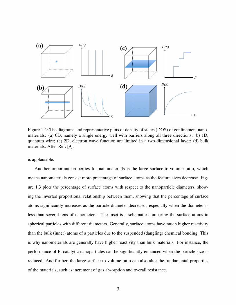

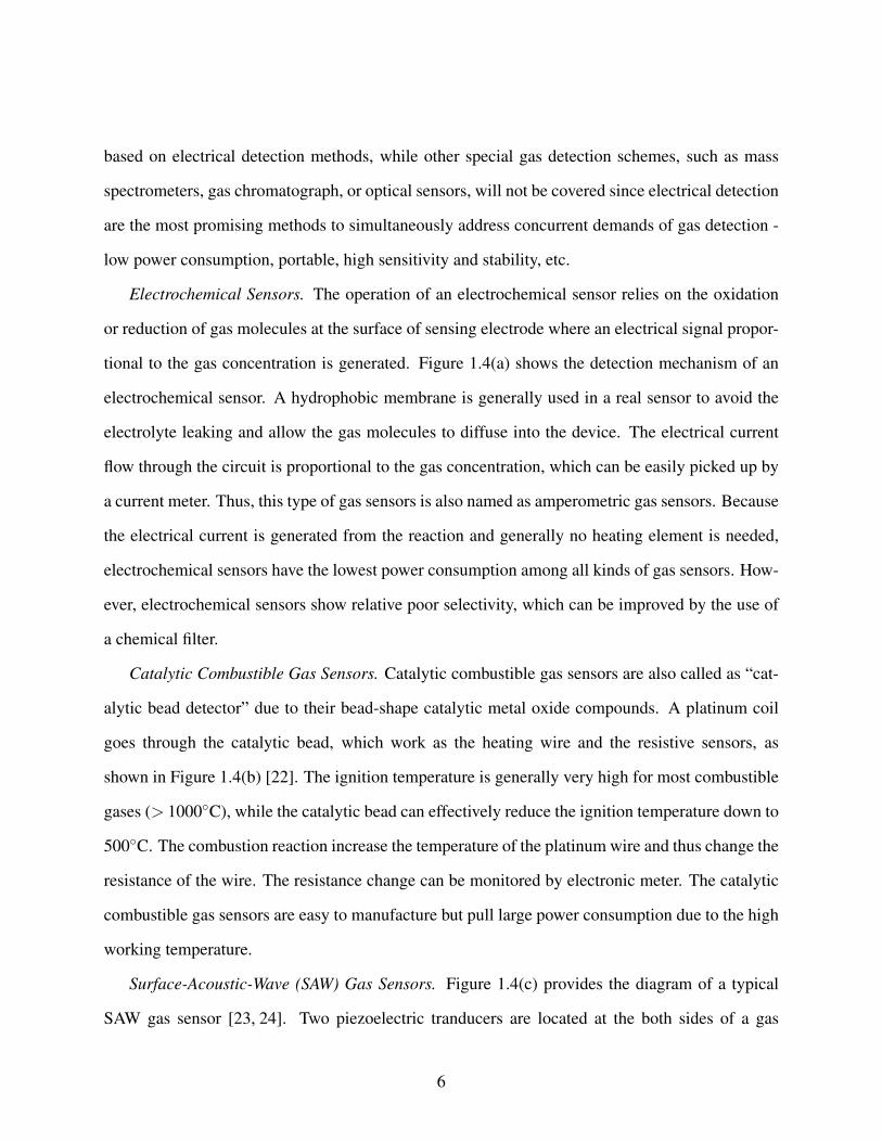


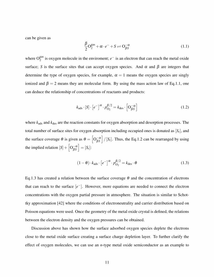
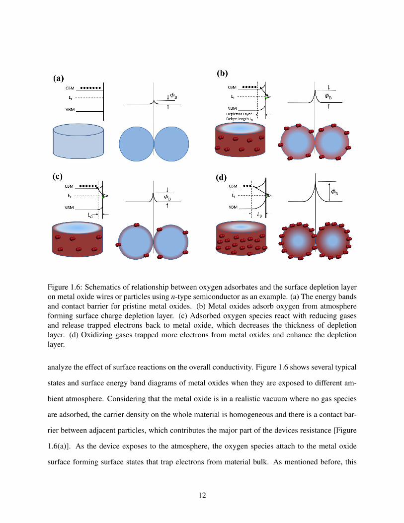

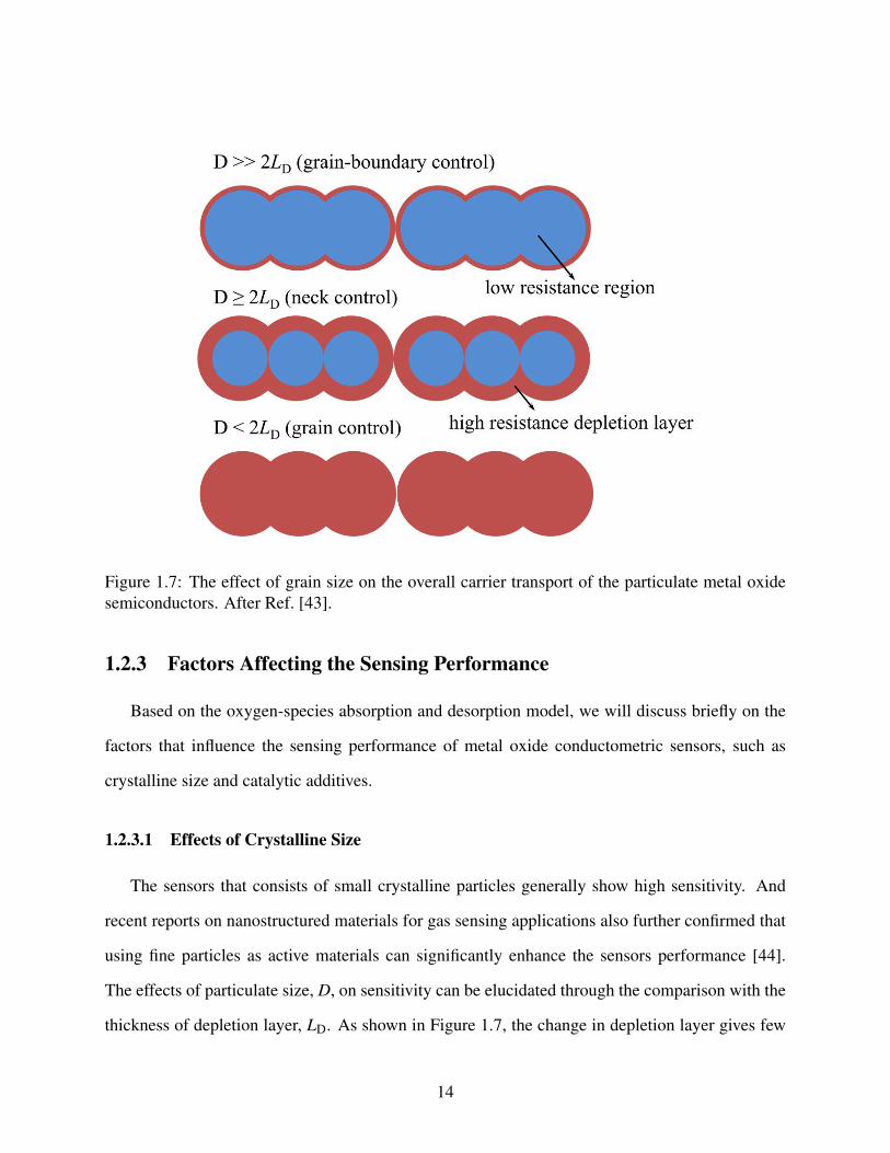

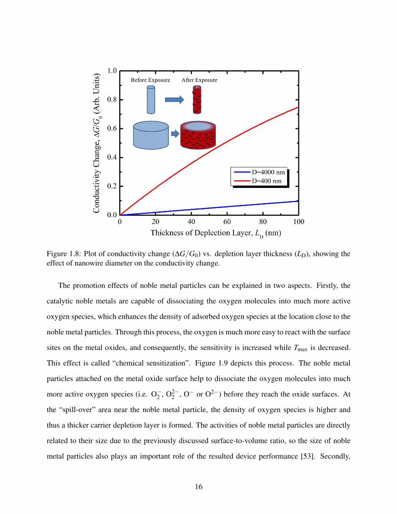

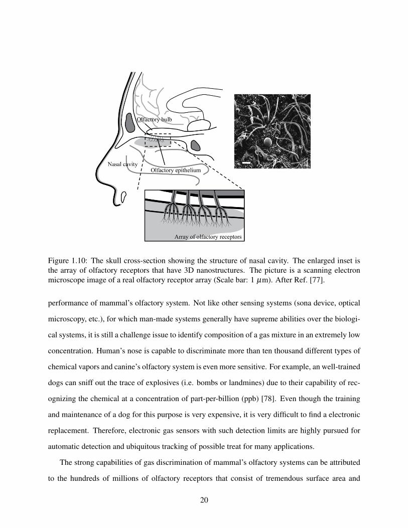
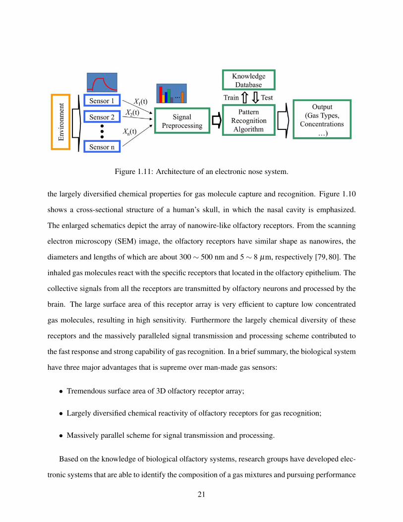
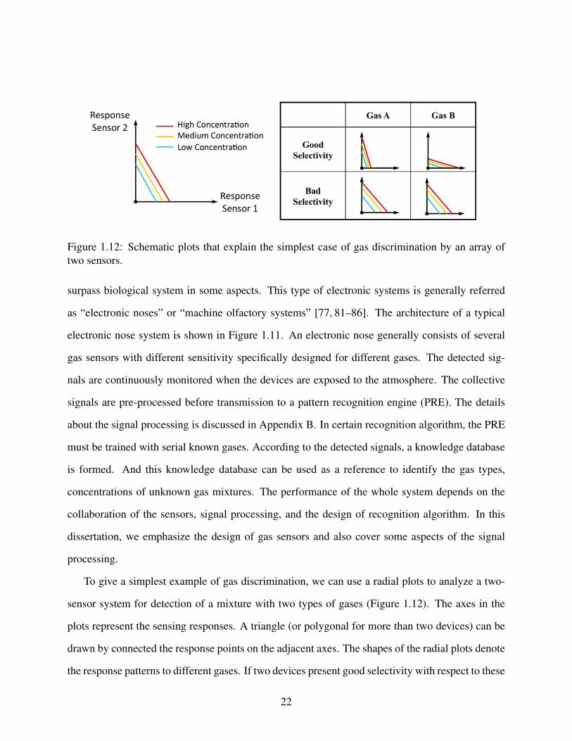
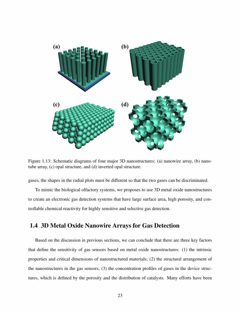
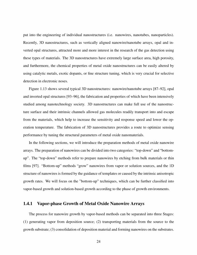

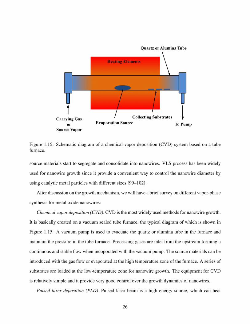
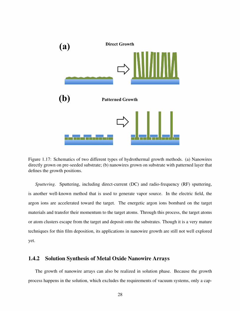
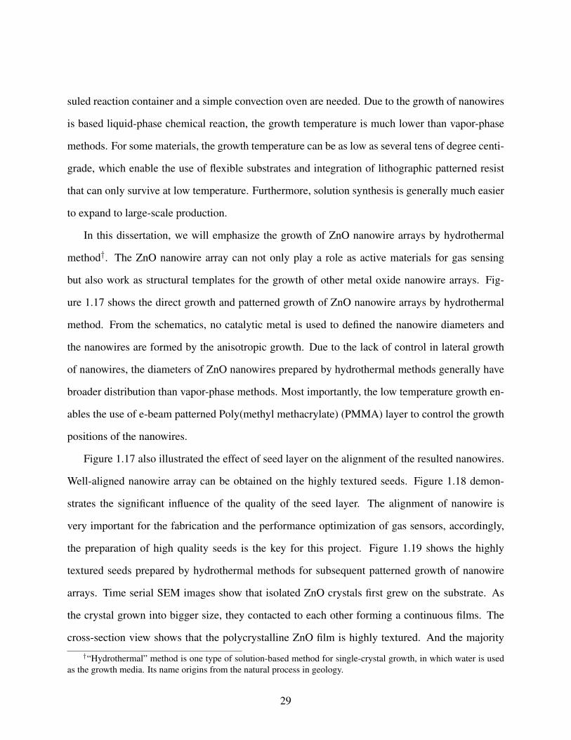


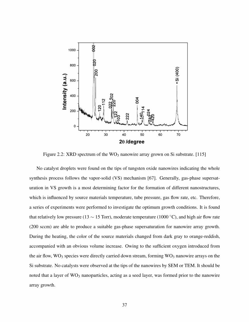

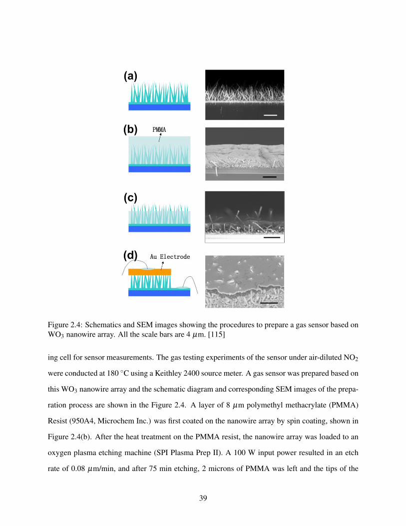
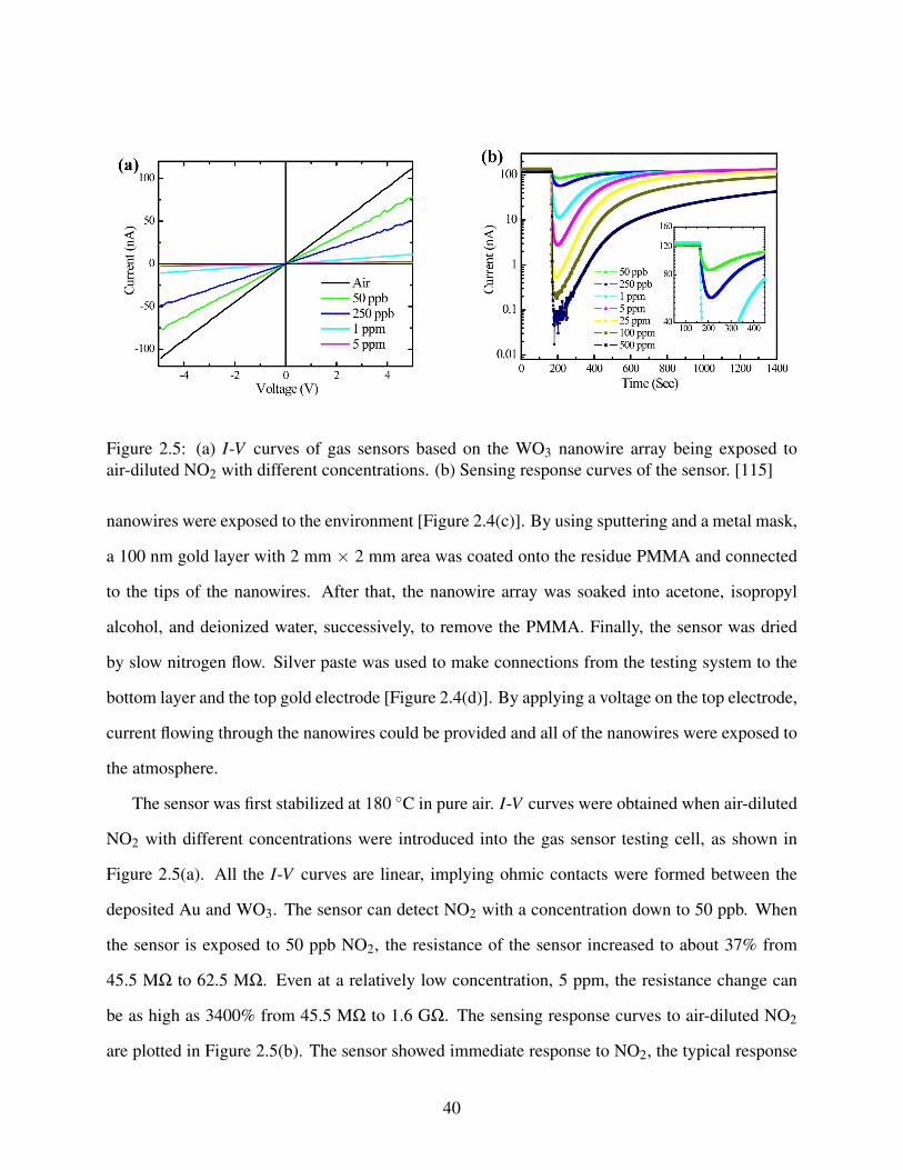

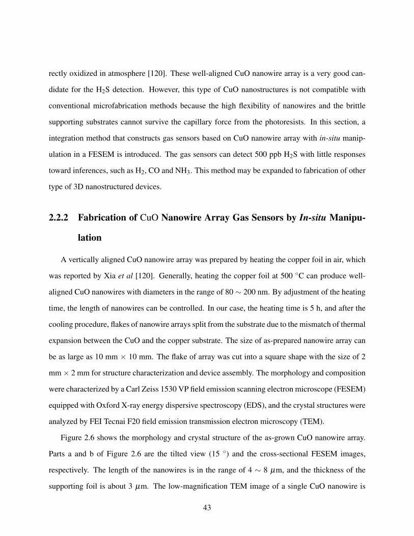
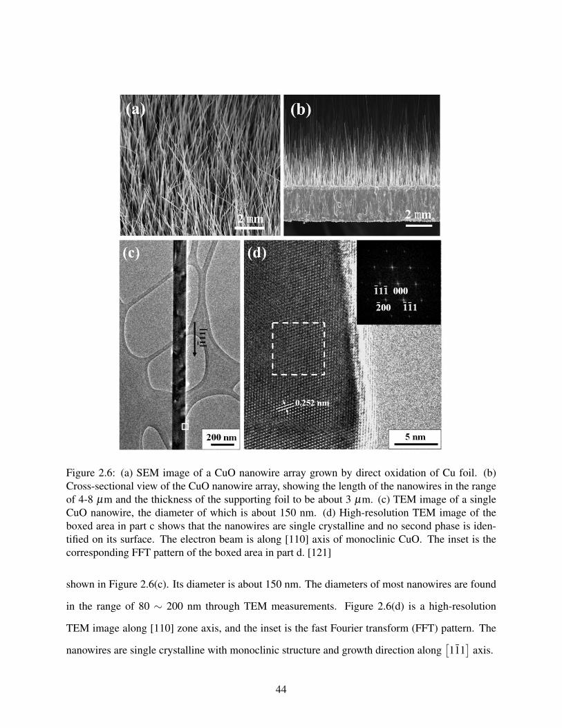
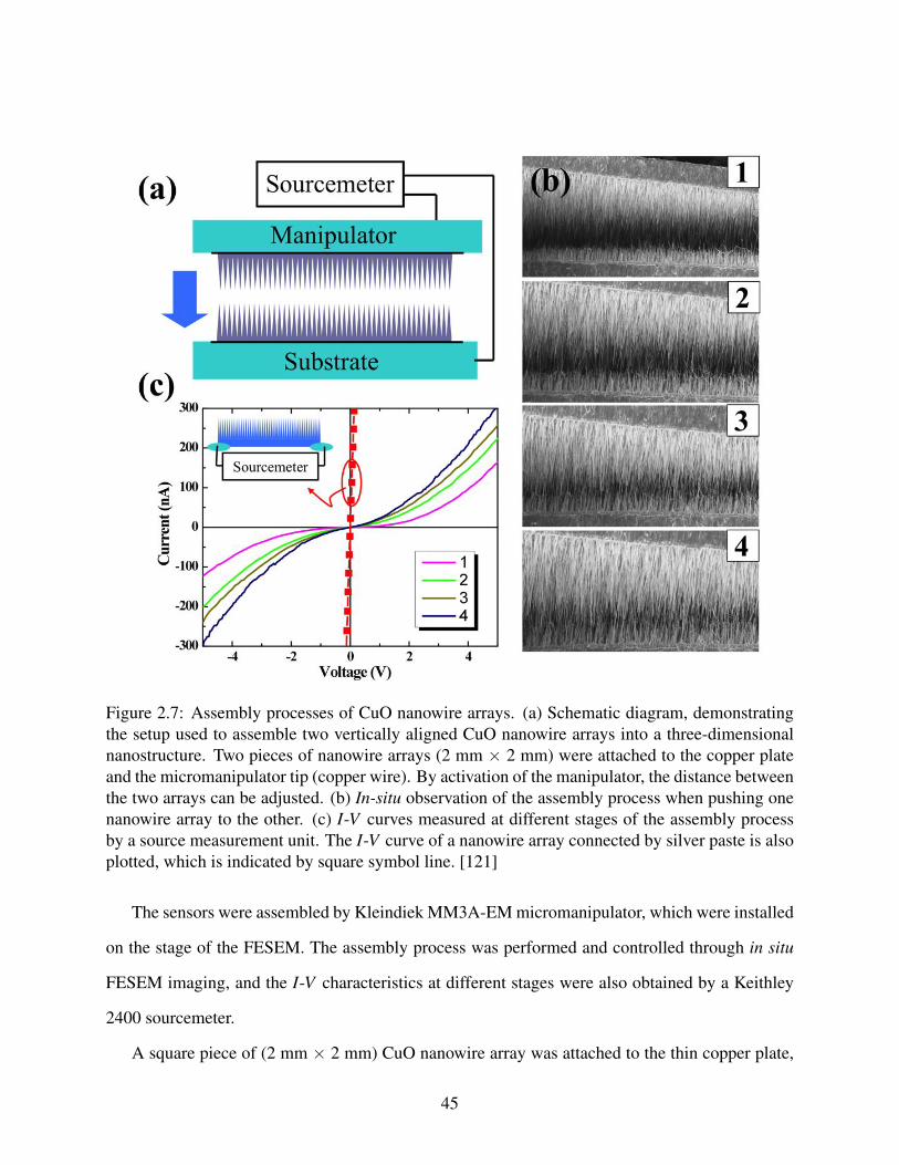

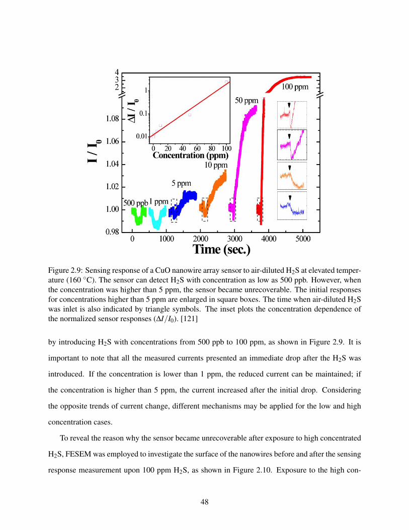
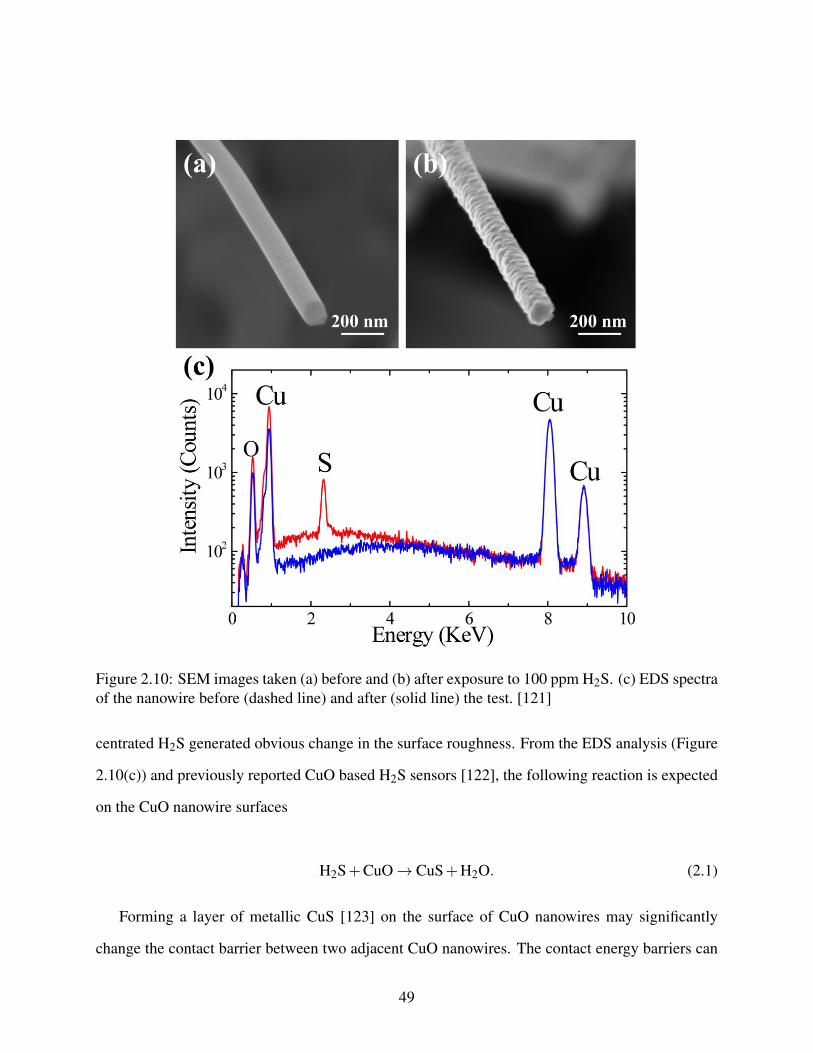
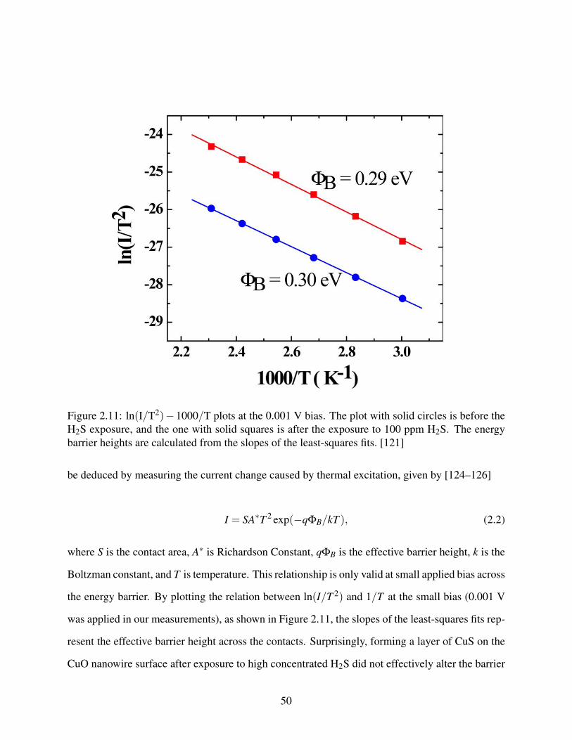
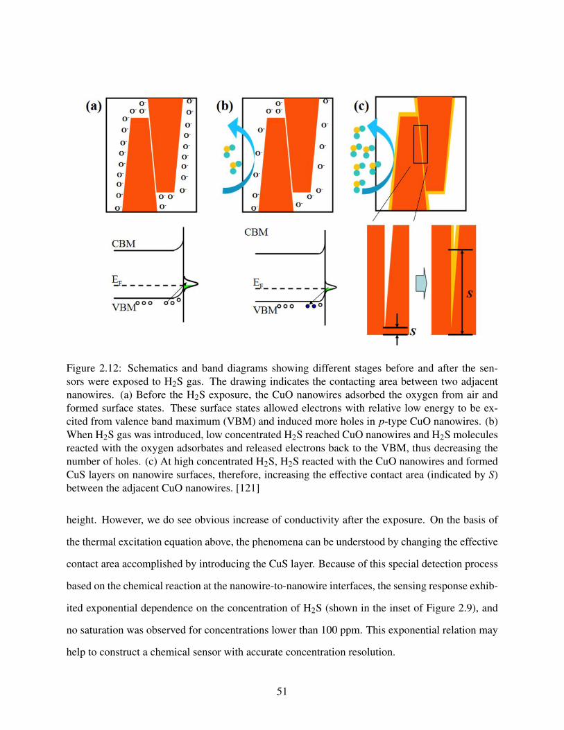

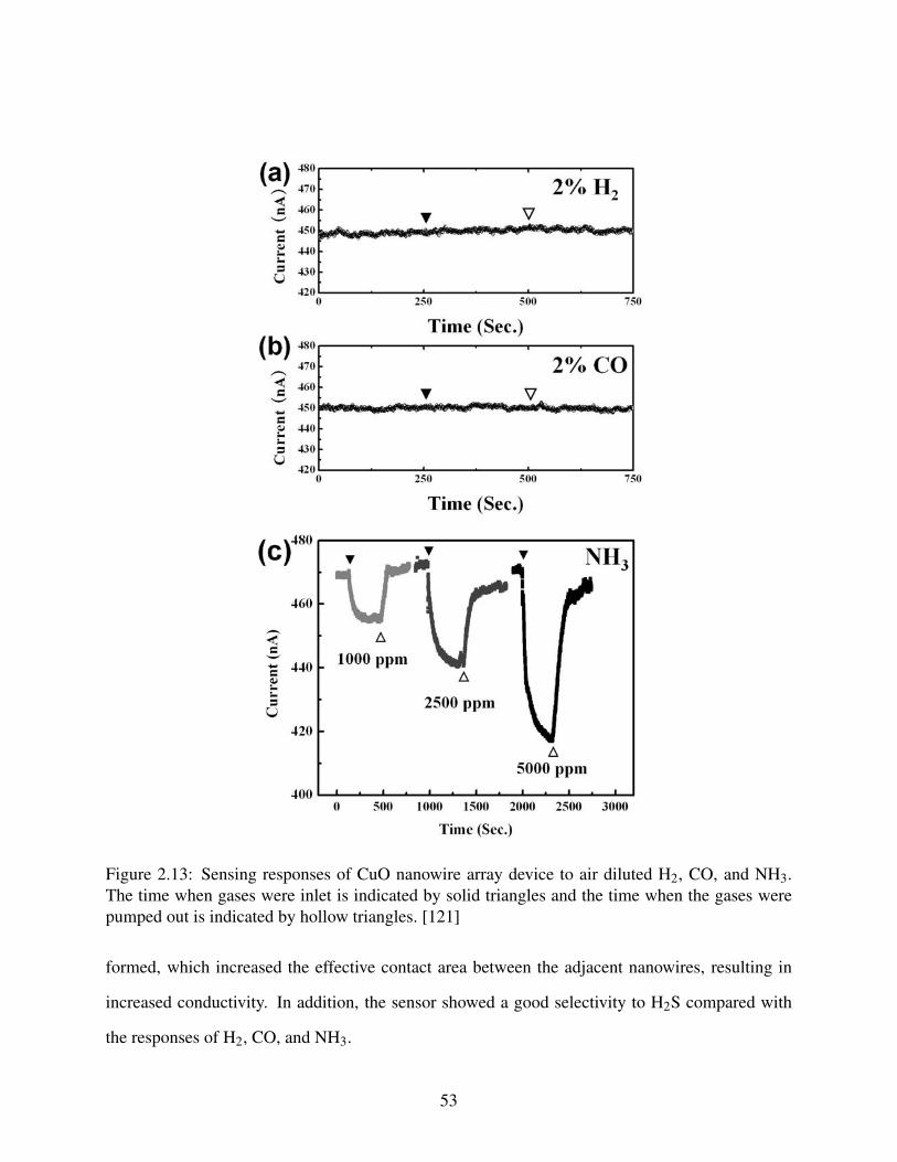
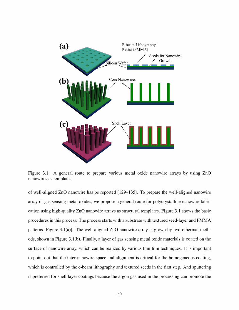


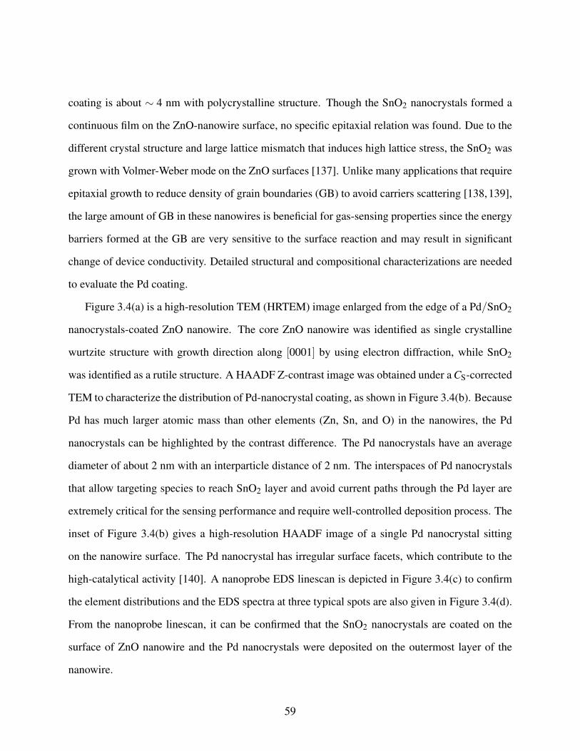

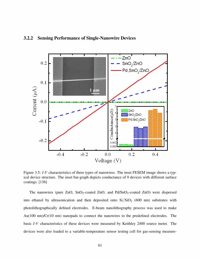
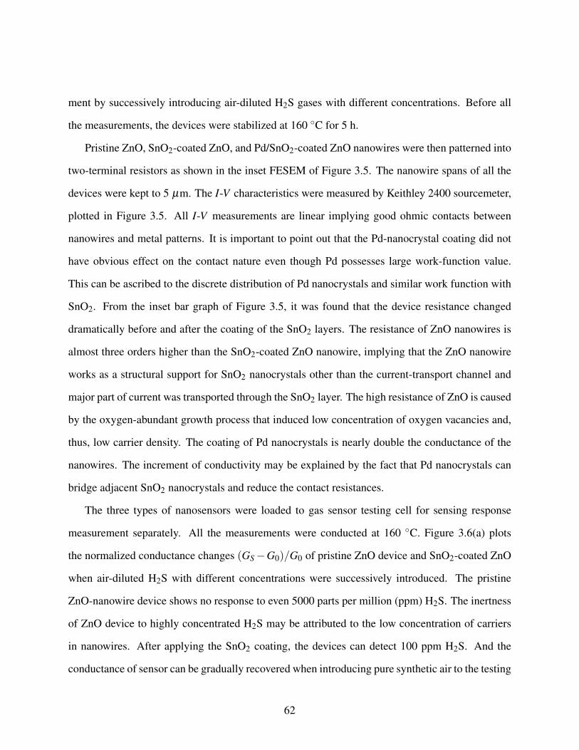


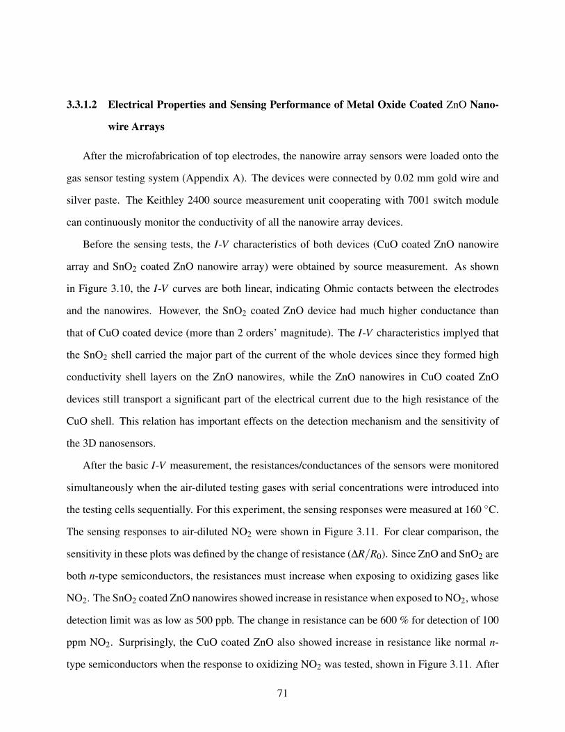

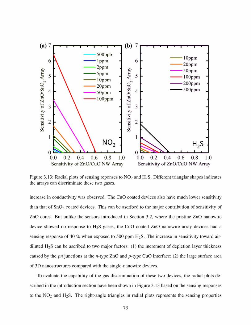


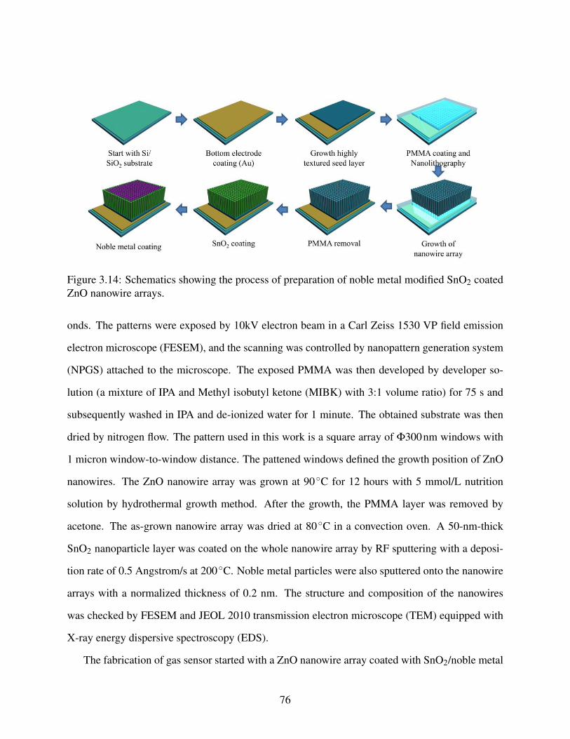

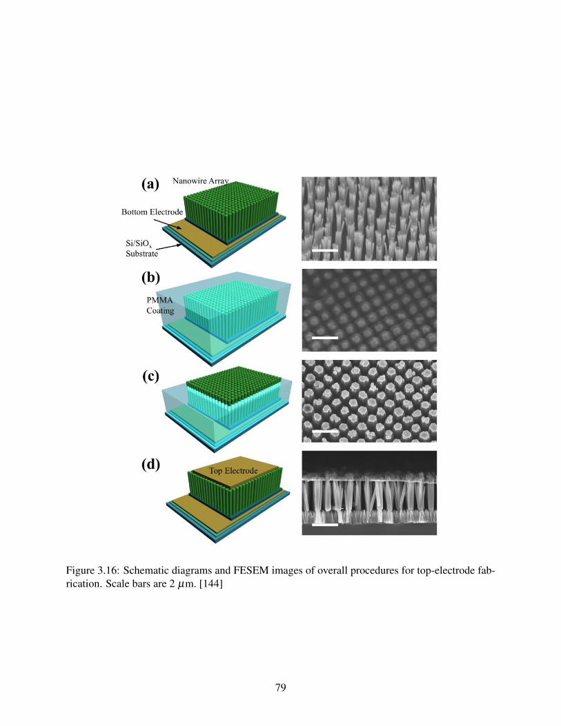
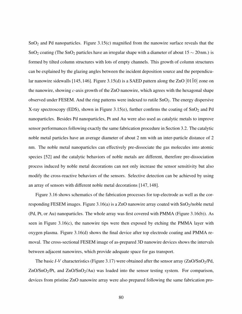

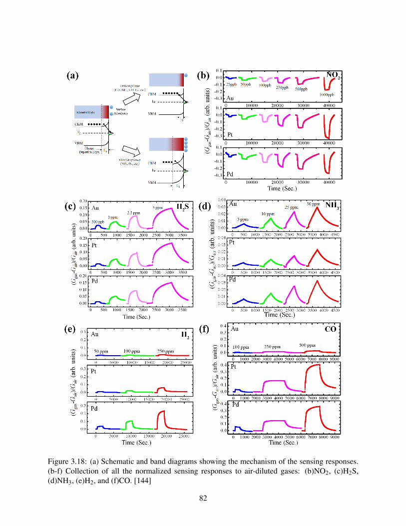
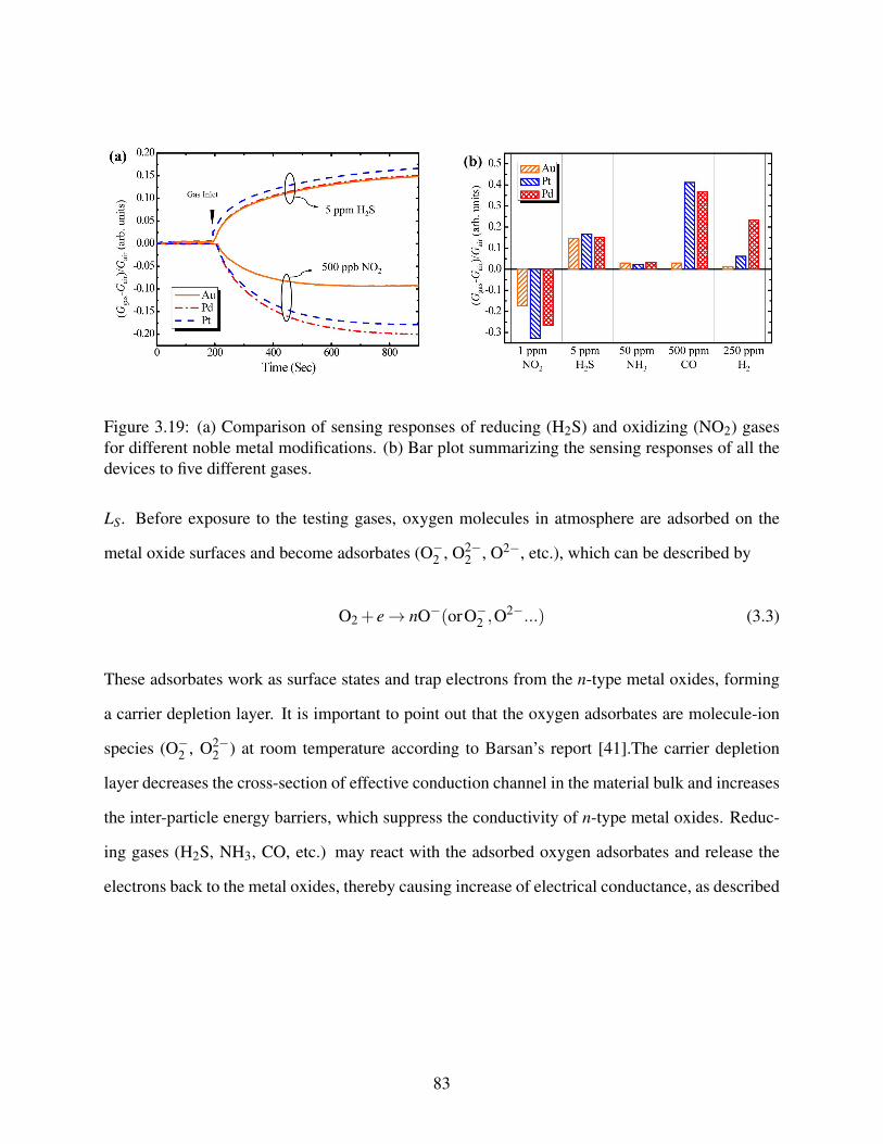
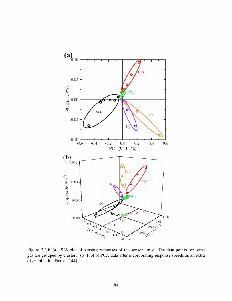


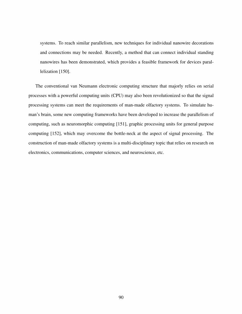

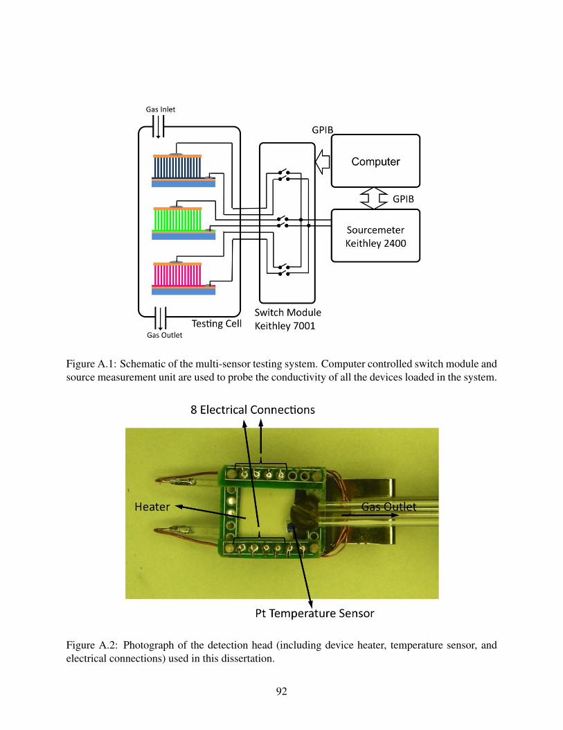
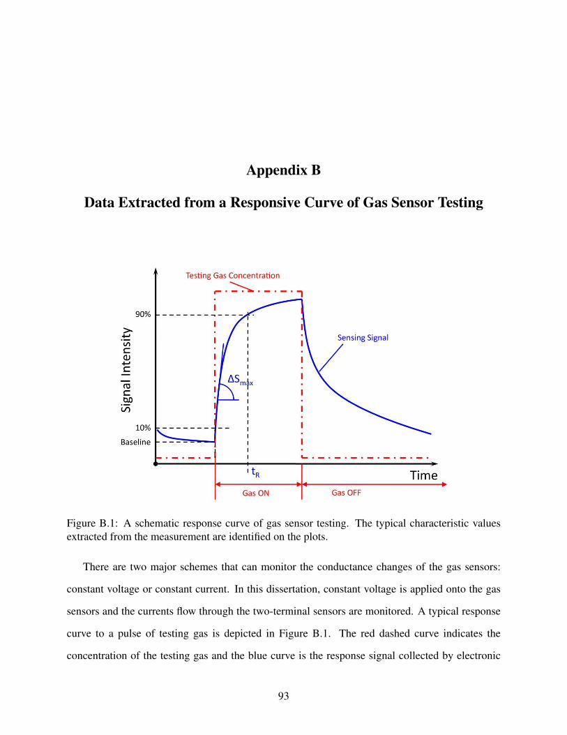

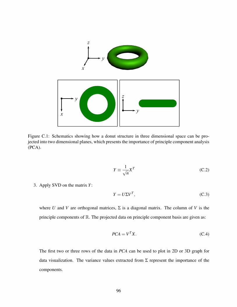


![Efficient Growth of Vertically-Aligned Single-Walled …maruyama/papers/17/VA-SWNT...Immediately after this, a scaled up production technique was developed [6]. Though vertically aligned](https://static.documents.pub/doc/80x56/5f2600b28469db656b3be722/efficient-growth-of-vertically-aligned-single-walled-maruyamapapers17va-swnt.jpg)


