High‐Performance Indoor VHF‐UHF Antennas: Technology Update Report 15 May 2010 (Revised 16 August, 2010) M. W. Cross, P.E. (Principal Investigator) Emanuel Merulla, M.S.E.E. Richard Formato, Ph.D. Prepared for: National Association of Broadcasters Science and Technology Department 1771 N Street NW Washington, DC 20036 Mr. Kelly Williams, Senior Director Prepared by: MegaWave Corporation 100 Jackson Road Devens, MA 01434
Transcript
High‐Performance Indoor VHF‐UHF Antennas:
Technology Update Report
15 May 2010
(Revised 16 August, 2010)
M. W. Cross, P.E. (Principal Investigator)
Emanuel Merulla, M.S.E.E.
Richard Formato, Ph.D.
Prepared for:
National Association of Broadcasters
Science and Technology Department
1771 N Street NW
Washington, DC 20036
Mr. Kelly Williams, Senior Director
Prepared by:
MegaWave Corporation
100 Jackson Road
Devens, MA 01434
2
Contents:
Section Title Page
1. Introduction and Summary of Findings……………………………………………..3
2. Specific Design Methods and Technologies Investigated…………………..7
3. Conclusions and Design Recommendations………………………………….128
3
1.0 Introduction and Summary of Findings In 1995 MegaWave Corporation, under an NAB sponsored project, developed a broadband VHF/UHF set‐top antenna using the continuously resistively loaded printed thin‐film bow‐tie shown in Figure 1‐1. It featured a low VSWR (< 3:1) and a constant dipole‐like azimuthal pattern across both the VHF and UHF television bands.
Figure 1‐1: MegaWave 54‐806 MHz Set Top TV Antenna, 1995
In the 15 years since then much technical progress has been made in the area of broadband and low‐profile antenna design methods and actual designs. These improvements have been published in: technical textbooks, peer‐reviewed articles, patents, government research and development reports, and seminar proceedings. As a developer of advanced antenna systems, primarily for the U.S. government, MegaWave constantly reviews these sources and acquires the latest computer based EM simulation tools in order preserve its competitive advantage. In this project, this knowledge was used to identify ten candidate design methods and technologies that have the potential to materially improve the performance of indoor VHF‐UHF TV antennas. This report describes each candidate and its potential to improve indoor ”set‐top” reception of DTV signals between 54 and 698 MHz. Of course, it must be kept in mind that, while advanced design methods and actual physical designs exist, so do the laws of electromagnetics. Maxwell’s equations have resulted both in practical as well as, what Dr. R. C. Hansen humorously calls, “Pathological Antennas”. These pathological designs are described in his most recent textbook [1], especially in the area of electrically‐small and broadband designs. It is instructive to apply these fundamental limitations to the problem at hand, the set‐top TV antenna.
Consider that a half‐wavelength in the low VHF TV band varies between 9.2 and 5.6 feet; between 34 and 27 inches in the high VHF band and between 12.6 and 8.5 inches in the UHF (470‐698 MHz) band. A dipole antenna whose physical length is less than its wavelength divided by pi (λ/π) is considered to be an electrically “small” antenna (ESA). ESAs unfortunately are characterized by narrow bandwidths and low gains. Assuming 2 to 3 feet as a maximum acceptable length for an indoor or set‐top antenna, it definitely falls into the ESA category in the low VHF band. But, in addition to size constraints and the resulting difficulty in obtaining acceptable performance from a single antenna over the 54 to 698 MHz spectrum, there are other concerns. Indoor and set‐top antennas are fundamentally disadvantaged due to building penetration losses and by proximity to sources of manmade radio noise. The former effect is more pronounced at UHF and the latter at low VHF channels. Both can have a significant deleterious effect on antenna performance. This brief discussion highlights the difficult problems inherent in designing efficient, high performance antennas for the indoor/set‐op TV environment. Fortunately, emerging technologies may effectively address these concerns. This report is organized as follows. Sections 2.1 through 2.10 contain summaries of each advanced method and hardware technology identified as a potential candidate for high‐performance indoor VHF‐UHF DTV antennas. Each section includes a list of references and, in many cases, photographs and performance data for multiple implementations of the technology that is described. Section 3 includes conclusions and a conceptual design for a practical indoor/set top VHF‐UHF antenna system. The authors evaluated each technology and arrived at the conclusions and design concept after sorting the nine hardware candidates into three categories as follows:
Mature technologies that do not require any CE‐909‐A channel designator or signal quality information from the DTV receiver:
o Fragmented Antennas (Section 2.2) o Non‐Foster Impedance Matching (Section 2.3)
Mature technologies that do require channel and quality data from the receiver:
o Active RF Noise Cancelling (Section 2.4) o Automatic Antenna Matching Systems (Section 2.5) o Physically Reconfigurable Antenna Elements (Section 2.6)
Emerging technologies that show promise, but are not sufficiently mature or practical at this time:
o Metamaterials (Section 2.7) o Electromagnetic Band Gap (EBG) Materials (Section 2.8) o Fractal/Self Similar Antennas (Section 2.9) o Retrodirective Arrays (Section 2.10)
5
A common thread connects each of these technology areas: advanced computational methods.
Whether a particular technology is mature and immediately applicable or emerging and highly
speculative, various schemes for antenna design optimization are universally applicable and
described in Section 2.1. These methodologies apply to all of the candidate technologies
discussed in Sections 2.2 through 2.10, and accordingly was placed at the beginning of Section
2. If even one of the optimization algorithms described had been available during the
development of MegaWave’s 1995 broadband set top antenna, it is likely that markedly better
gain performance would have resulted, especially in the low and high VHF bands. Another
attractive and potentially very significant capability offered by optimization algorithms is the
possibility of discovering entirely new antenna geometries, rather than simply optimizing a pre‐
existing geometry.
Table 1‐1 subjectively ranks the nine identified candidate hardware technologies (2.2 ‐ 2.10). A
score of 10 represents perfection. By maturity we mean how close to off‐the‐shelf a particular
technology’s hardware is and how well it basic principle of operation has been vetted in the
literature. The term SWAP refers to size/weight and power.
Method/ Technology
Active/ Passive
RequiresCE‐909‐A Interface
Maturity Vetted Risk Design Complexity
SWAP Comments
2.1 Adv. Comp. Methods
N/A N/A 9 9 Very Low N/A N/A Applies to all Technologies
2.2 Fragmented Passive No 7 7 Low Low 9 Planar
2.3 Non‐Foster Active No 6 7 Low Moderate 7 Limited Bandwidth
2.4 Active Noise Cancelling
Active Yes 7 6 Low High 3 Requires I&Q
2.5 Automated Antenna Matching
Active Yes 7 7 Moderate High 7 Requires complex TV interface
2.6 Reconfigurable Antennas
Active Yes 6 7 Moderate High 6 Control of MEMS w/DC
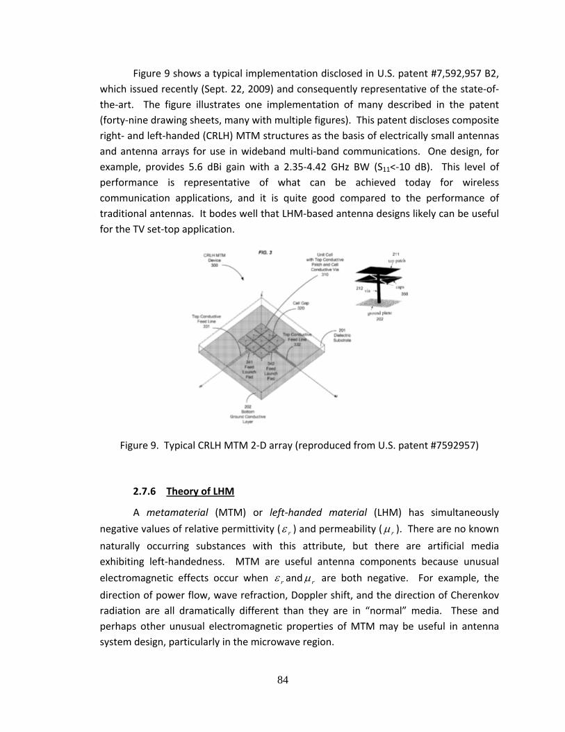
2.7 Metamaterials Passive No 3 4 High High 8 Emerging/Availability an issue
2.8 EBG Passive No 5 6 High High 5 Inherently Narrow Band Maybe useful for shielding
2.9 Fractal/Self Similar
Passive No 6 4 Moderate Moderate 8 Controversial Performance Gain
2.10 Retrodirective Active Yes 4 5 Very High Very High 2 Narrow ‐Band, Large
Table 1‐1: Candidate Technologies Considered and Their Ranking
6
As an example of how advanced computational methods could be combined with an advanced hardware technique, that does not require a CE‐909‐A interface, is described at the end of Section 3 and summarized here.
Using the genetic algorithm described in Section 2.1.5 a fragmented antenna was designed and combined with a non‐Foster‐matching circuit to provide a planar 54‐698 MHz dipole approximately 13 by 13 inches with significantly better gain, especially in the 54‐88 and 174‐216 MHz bands, than the 1995 MegaWave/NAB set top antenna. Figure 1 shows the broadband fragmented planar element’s design obtained after approximately 24 hours of computational time on a PC. Details of the specific method used are in Section 2.2 of this report. It is well matched across the UHF DTV band, but requires some passive matching in the high VHF band (which would also serve as the band combiner) and the more robust matching capability of the active Non‐Foster‐Matching technique, described in Section 2.3, for the low‐VHF band.
Figure 1. 13 x 13 Inch Planar Fragmented Non‐Foster Matched VHF‐UHF Antenna
An omni‐directional version could also be designed. It should be stressed that the above is included here only to illustrate the notion of combining advanced computational broadband antenna element designs with emerging electronic antenna matching capabilities and that other antenna element geometries are also possible, depending on the starting conditions, trade space dimensions and performance goals provided to the optimizer.
The authors want to make clear that 90 percent of the techniques and ideas contained in this study are the work of others, as published in the open literature and referenced herein.
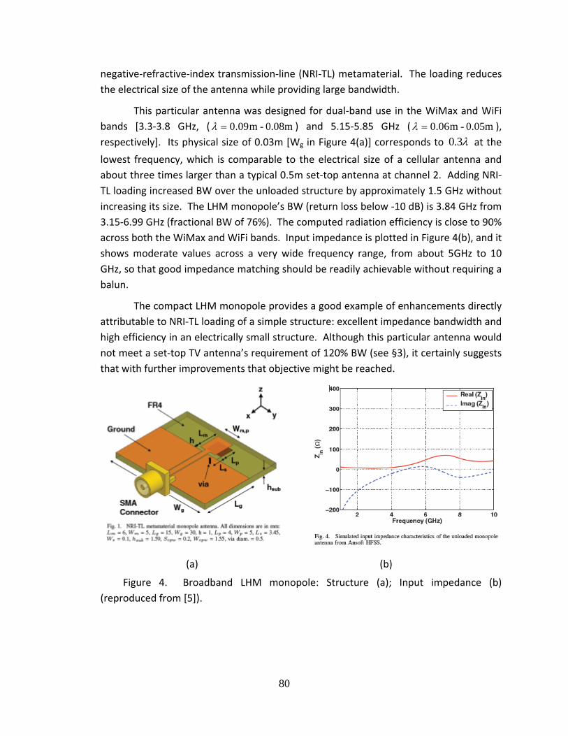
7
2.0 Specific Design Methods and Hardware Technologies Investigated
2.1 Advanced Computational Methods
2.1.1 Summary
Optimization methodologies abound, and they are extensively used in every
aspect of engineering design, in particular antenna design. Optimization algorithms are
useful in two ways. They can be used to optimize the design parameters for a user‐
specified antenna geometry (for example, element spacing, length and diameter in a
Yagi‐Uda array). They also can generate designs that are impossible to achieve
otherwise. In both cases, optimization involves meeting specific performance objectives
(typically, VSWR, gain, bandwidth, and so on).
Optimization algorithms have become progressively more important as the
limitations of classic analytical techniques have become progressively more apparent.
While the equations underlying electromagnetic theory are well understood and
accurately describe all electromagnetic phenomena, in most practical cases they cannot
be solved analytically or, oftentimes, even numerically. Designing better antennas
requires improved methodologies, and state‐of‐the‐art optimization algorithms have
proven very effective. There is no question that these techniques are applicable to the
set‐top antenna design problem, and that they should receive considerable attention in
future design activities.
There are many different optimization methodologies that fall into two broad
categories: analytical methods and heuristic methods. Analytical methods are based on
precise mathematical formulations of the optimization problem. Even though they may
be fundamentally numerical in nature, they involve standard mathematical operations
such as computing derivatives or evaluating integrals. Heuristic methods may involve
equations, but the equations are not the result of an analysis. Instead, they are offered
without “proof” based on the fact that they “work.”
Many optimization heuristics are Nature inspired. The steps an algorithm
performs to optimize an antenna are based, for example, on how bacteria forage for
food. As disparate as these entities may seem, there is a connection, at least in the
sense that bacteria finding a good food source is similar to finding an antenna with a
good gain‐bandwidth product. Optimization algorithms of this type are usually referred
to as “metaheuristics,” a term intended to emphasize that the method is both empirical
and conceptual in nature. Thus, an effective bacteria foraging algorithm can be
implemented in many different ways because the bacteria foraging metaheuristic simply
suggests an analogy to Nature that is implemented in a computer algorithm working on
8
an antenna problem. The metaheuristic thus is an algorithmic framework instead of a
list of steps or instructions.
Several Nature inspired metaheuristics are described. A brief summary of each
algorithm is provided, and several example antenna problems solved by a variety of
algorithms are discussed. The algorithms include Ant Colony Optimization (ACO),
Central Force Optimization (CFO), Invasive Weed Optimization (IWO), Intelligent Water
Drop (IWD) algorithm, and Bacteria Foraging Optimization (BFO). There are many other
optimization algorithms [for example, Space Gravitation Optimization (SGO), Integrated
Radiation Optimization (IRO)], but they have not been applied to antennas or antenna
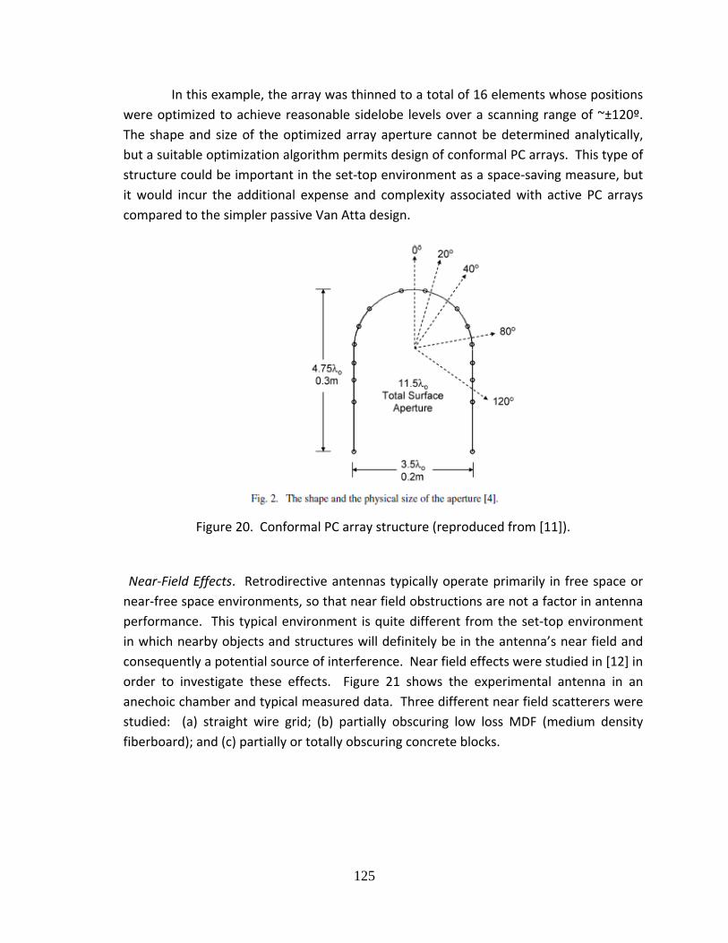
related problems.
Each of these algorithms, except one, is inherently stochastic because its Nature
inspired algorithmic model relies on randomness in its functioning. The underlying
equations contain true random variables whose values are computed from a probability
distribution and consequently cannot be known in advance. As a result, every time a
stochastic optimizer run is made, its results are different than the previous run even
when exactly the same run setup parameters are used. The performance of stochastic
optimizers is necessarily characterized statistically (for example, average values,
standard deviations). This may be a limitation in the utility of optimization algorithms if
they are used in a set‐top antenna on a real time basis. For example, a self‐structuring
antenna (SSA) must reconfigure itself in real time in response, for example, to a
changing environment.
The one algorithm that is not inherently stochastic is Central Force Optimization
(CFO) whose Nature inspiring metaphor is gravitational kinematics, the branch of
physics that deals with the motion of masses moving under the influence of gravity. The
underlying equations are Newton’s equations of motion, which are completely
deterministic. CFO analogizes these equations in “CFO space” by flying “probes” that
are similar to small satellites to search a decision space “landscape” for the maximum
(optimal) values of a function (for example, antenna gain as a function of element length
and polar angle). CFO has been applied to antenna design and network synthesis, and
tested against many recognized benchmark functions used to evaluate optimization
algorithms. It therefore may be especially useful for the set‐top antenna problem.
2.1.2 Introduction
This section describes developments in antenna design optimization over the
past fifteen years or so that have been driven largely by the availability of progressively
more powerful computers. A plethora of new optimization algorithms have been
9
introduced and tested and are now in widespread use. The new antenna designs often
are non‐intuitive, occasionally even counter‐intuitive, but all share the common feature
of not being accessible in any other way. State‐of‐the‐art optimization algorithms can
effectively solve intractable problems that have no analytical solutions or are too
complex to apply traditional analytical techniques. These approaches are useful right
now in designing set‐top television antennas, and they will continue to be useful
whatever form future set‐stop systems take. Some of the more important and
interesting optimization algorithms are described here.
Optimization Methodologies. The problem of locating the maximum values of a
function is generally referred to as “multidimensional search and optimization.” As
pointed out above, any problem involving three or more design parameters (“decision
variables”) is a multidimensional problem, and simple methods such as plotting the
function to be maximized cannot be used. Methods for solving these problems fall into
two broad categories: analytical methods and heuristic methods. Analytical methods,
which involve computing derivatives and gradients, are of limited use, especially in the
complex landscapes associated with antenna design. Stringent performance
requirements in terms of bandwidth, radiation pattern, and standing wave ratio (SWR)
make antenna optimization problems particularly difficult because the landscape is
usually extremely multimodal with narrow resonances and often high sensitivity to
slight parameter variations. Heuristic optimization methodologies, which are inherently
numerical in nature, are effective in dealing with these issues, and consequently they
are considered here while analytical approaches are not.
An entire class of heuristic optimization algorithms are “Nature inspired”, and
these appear to be the most effective. A Nature inspired algorithm is a computer search
and optimization program whose function mimics some natural process. These
programs are described as being “metaphorical” because they analogize some natural
process without precisely modeling it. For example, “Ant Colony Optimization” (ACO) is
an algorithm that simulates (to some degree) the behavior of ants seeking food. Thus,
ACO is inspired by the metaphor of ant foraging. All such algorithms evolve a solution to
the optimization problem over a series of steps or iterations, and almost all such
algorithms are stochastic population‐based methodologies. An initial population (of
ants, for example) randomly (stochastically) moves through the decision space
(landscape) step‐by‐step (iterating) in such a way that it converges on the largest food
supply (maximum function value). The ants’ progress is controlled by a set of equations
that mimic real ant behavior in Nature. There are many Nature inspired algorithms,
ACO being one of the earliest ones. The more important algorithms are discussed below
with examples of their application to antenna optimization.
10
2.1.3 Ant Colony Optimization
Figure 1 illustrates the basic idea behind Ant Colony Optimization (ACO) [1]. The
irregular objects represent the ants’ nest (bottom) and a desirable source of food (top).
It has been observed that ants seeking food eventually traverse the shortest path
between the nest and food by marking that trail with a chemical pheromone that each
ant can sense (probably by smell). If the path is unobstructed [(a) in the figure], then
the ants simply walk a more‐or‐less straight line between home and the food supply.
But, if an obstruction is imposed [(b) and (c) in the figure], then more ants eventually
end up on the shorter trail between the food and the nest, which in turn results in a
greater pheromone concentration along that “optimal” trail. By depositing
progressively more pheromone on the shortest path, almost all of the ants eventually
end up on that path, and the “best” solution has been found. The red lines in the
bottom part of the diagram illustrate the path evolution with the eventual result that
the shortest path is identified.
The ACO algorithm mimics the ants’ behavior using equations that represent the
random motion of individual ants subject to their pheromone environment. Instead of
searching for food, the metaphorical ACO ants search the landscape of a decision space
for the maximum value of the function to be maximized. But the process they follow is
a simplified model of ant behavior as observed in Nature. And, just as real ants
eventually discover the best food source, ACO’s “ants” eventually converge on the
function’s global maximum value.
Figure 1. Ant Colony Optimization Metaheuristic (reproduced from [1]).
11
2.1.4 Particle Swarm Optimization
Particle Swarm Optimization (PSO) [2] is another stochastic population‐based
Nature inspired evolutionary algorithm. PSO analogies the swarming behavior of fish or
bees seeking food. Unlike ACO in which each “ant” creates a pheromone trail for other
ants to follow, PSO’s population of “agents” collectively communicate two pieces of
information: each individual agent’s “best” solution (greatest food concentration) and
the population’s overall (global) best solution. Equations that mimic bee and fish
swarming then control each agent’s subsequent motion in the decision space based on
the competing tendencies of moving toward the global best and randomly exploring the
vicinity of its best solution. As shown in Figure 2 for bees swarming around a flower
concentration, after many steps PSO agents converge on the global best solution
(highest flower concentration) because the local search fails to reveal any better
solutions.
Figure 2. Particle Swarm Optimization metaheuristic (reproduced from [2]).
2.1.5 Genetic Algorithms
A Genetic Algorithm (GA) [3] analogizes the process of natural evolution or
“survival of the fittest.” When biological parents “mate,” they exchange DNA to create
a new individual (“child”) whose characteristics are drawn from both parents by
combining the parents’ DNA. A GA creates successive generations of children who then
serve as parents for the next generation whose children, in turn, will exhibit better
“fitness” than the previous generation. In the context of search and optimization, the
fitness is the value of the function to be maximized, so that the “best” fitness
corresponds to the function’s global maximum. As the GA progresses generation after
generation, the best discovered fitness improves and eventually converges on the
function’s global maximum.
12
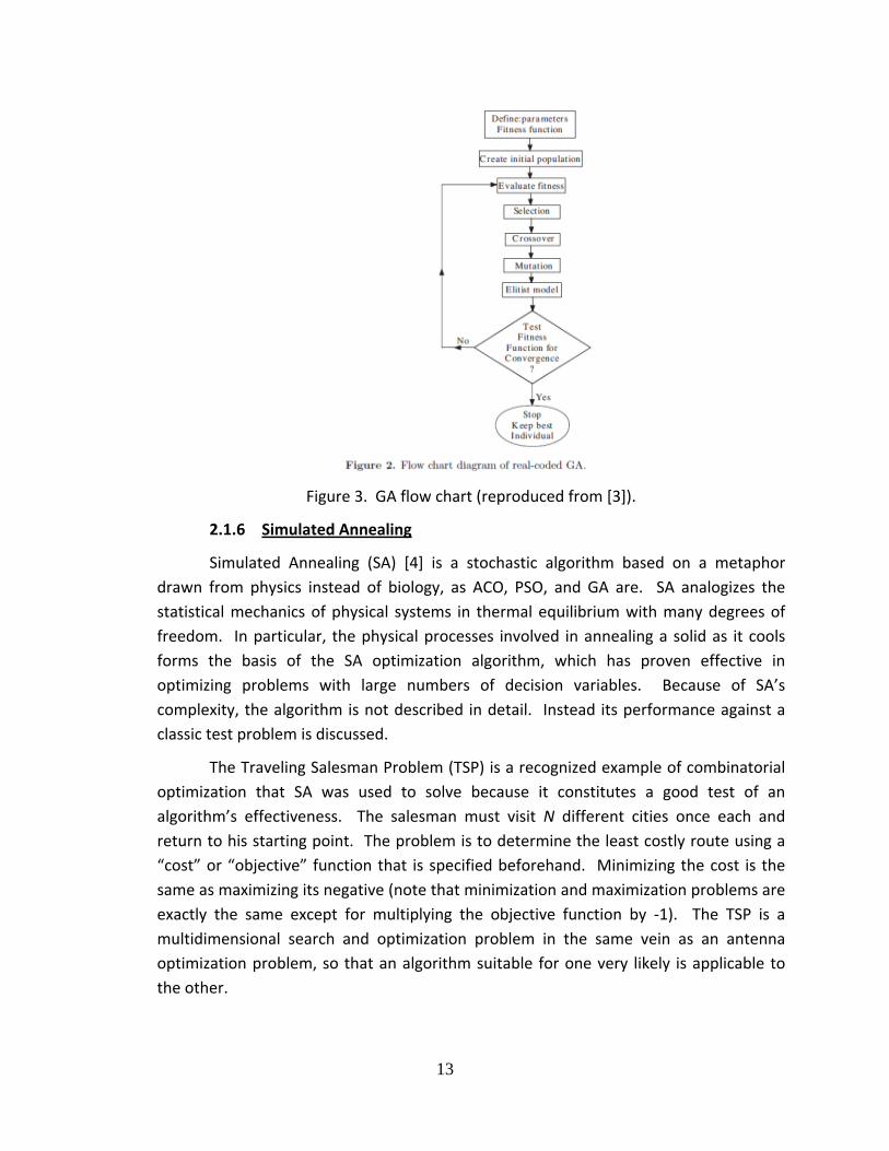
Figure 3 shows a typical GSA flowchart for an antenna optimization algorithm. It
starts with a definition of the decision space (parameters to be optimized) and the
“fitness function” to be maximized (for example, antenna directivity, or some specified
combination of performance parameters such as gain, bandwidth, and so on). An initial
population of “individuals” is randomly created, and each individual is defined by a
chromosome that may be a binary sequence or a real number. Each chromosome
comprises a set of genes, and each gene is one of the design parameters. For example,
if the three design parameters were element length, inter‐element spacing, and
element diameter in a four element Yagi‐Uda array, then there is a total of eleven
design parameters, and each one is a gene. Thus, the optimization problem is defined
on an 11‐dimensional decision space, and the objective is to determine each of the
eleven parameters so as to maximize some specific fitness function, say, the array’s
gain‐bandwidth product. A separate computer program is used compute the fitness at
each step for each chromosome (the “evaluate fitness” box in Figure 3).
After the initial population’s fitnesses are evaluated, the “selection” process
chooses two parent chromosomes that will mate (“crossover”) to produce two children
chromosomes in the next generation. The selection and crossover processes take many
varied forms. For example, the selection of parents may be random, or “best mates
worst,” or best pairs pair wise through the population, and so on. The crossover
operation likewise can take many forms. For example, the parents’ chromosomes may
be split at the midpoint with first and second parts being swapped, or a random break
point might be used, or some other combinatorial approach taken. Finally, the children
thus created are subject to some level of mutation, a random perturbation of the
chromosome structure just as real chromosomes are mutated in Nature. The steps
described thus far are essentially common to all Gas, but the next step in the flowchart
(“elitist model”) is not. In this GA, the worst individual in the new generation is replaced
by the best individual from the previous generation, thus preserving the best solution
from generation to generation as the algorithm progresses. As a final step, the best
fitness is tested for convergence, and the process repeated until convergence is
achieved.
13
Figure 3. GA flow chart (reproduced from [3]).
2.1.6 Simulated Annealing
Simulated Annealing (SA) [4] is a stochastic algorithm based on a metaphor
drawn from physics instead of biology, as ACO, PSO, and GA are. SA analogizes the
statistical mechanics of physical systems in thermal equilibrium with many degrees of
freedom. In particular, the physical processes involved in annealing a solid as it cools
forms the basis of the SA optimization algorithm, which has proven effective in
optimizing problems with large numbers of decision variables. Because of SA’s
complexity, the algorithm is not described in detail. Instead its performance against a
classic test problem is discussed.
The Traveling Salesman Problem (TSP) is a recognized example of combinatorial
optimization that SA was used to solve because it constitutes a good test of an
algorithm’s effectiveness. The salesman must visit N different cities once each and
return to his starting point. The problem is to determine the least costly route using a
“cost” or “objective” function that is specified beforehand. Minimizing the cost is the
same as maximizing its negative (note that minimization and maximization problems are
exactly the same except for multiplying the objective function by ‐1). The TSP is a
multidimensional search and optimization problem in the same vein as an antenna
optimization problem, so that an algorithm suitable for one very likely is applicable to
the other.
14
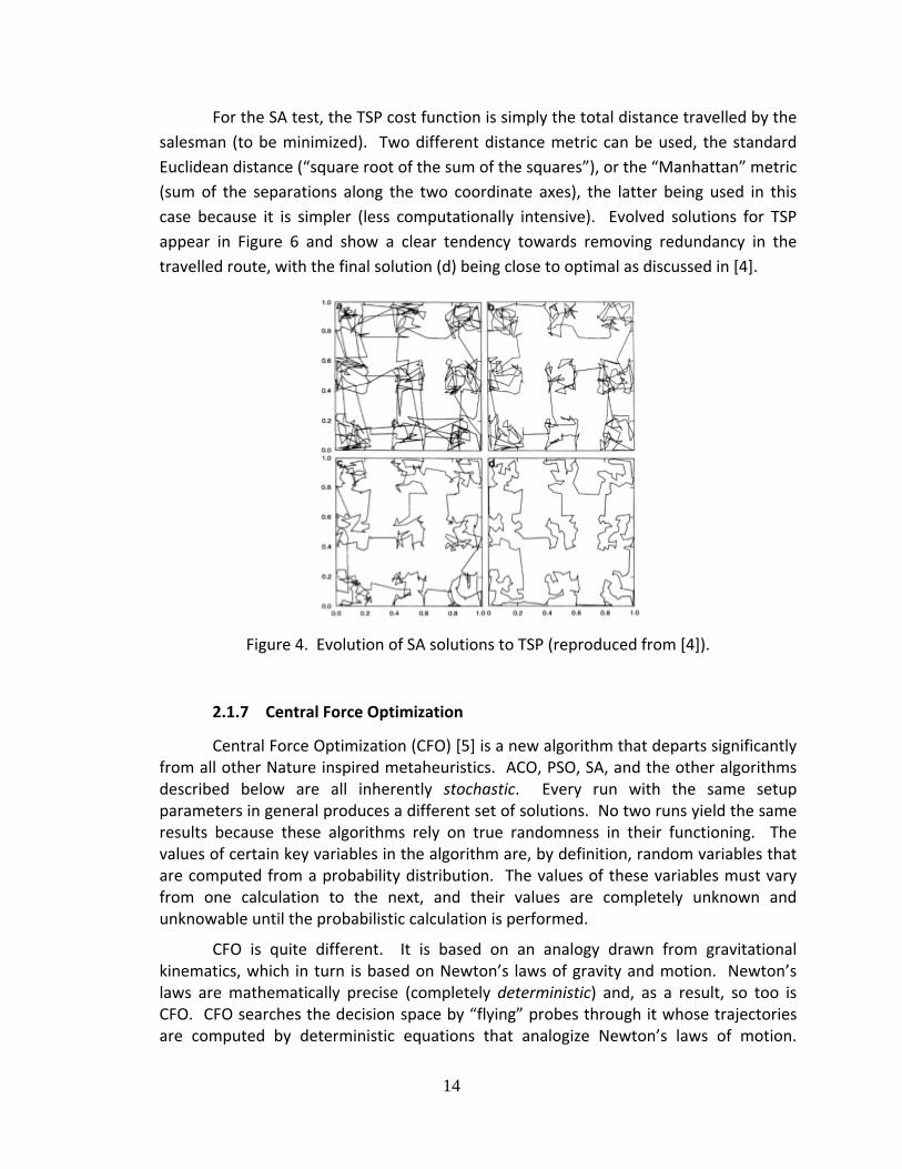
For the SA test, the TSP cost function is simply the total distance travelled by the
salesman (to be minimized). Two different distance metric can be used, the standard
Euclidean distance (“square root of the sum of the squares”), or the “Manhattan” metric
(sum of the separations along the two coordinate axes), the latter being used in this
case because it is simpler (less computationally intensive). Evolved solutions for TSP
appear in Figure 6 and show a clear tendency towards removing redundancy in the
travelled route, with the final solution (d) being close to optimal as discussed in [4].
Figure 4. Evolution of SA solutions to TSP (reproduced from [4]).
2.1.7 Central Force Optimization
Central Force Optimization (CFO) [5] is a new algorithm that departs significantly from all other Nature inspired metaheuristics. ACO, PSO, SA, and the other algorithms described below are all inherently stochastic. Every run with the same setup parameters in general produces a different set of solutions. No two runs yield the same results because these algorithms rely on true randomness in their functioning. The values of certain key variables in the algorithm are, by definition, random variables that are computed from a probability distribution. The values of these variables must vary from one calculation to the next, and their values are completely unknown and unknowable until the probabilistic calculation is performed.
CFO is quite different. It is based on an analogy drawn from gravitational kinematics, which in turn is based on Newton’s laws of gravity and motion. Newton’s laws are mathematically precise (completely deterministic) and, as a result, so too is CFO. CFO searches the decision space by “flying” probes through it whose trajectories are computed by deterministic equations that analogize Newton’s laws of motion.
15
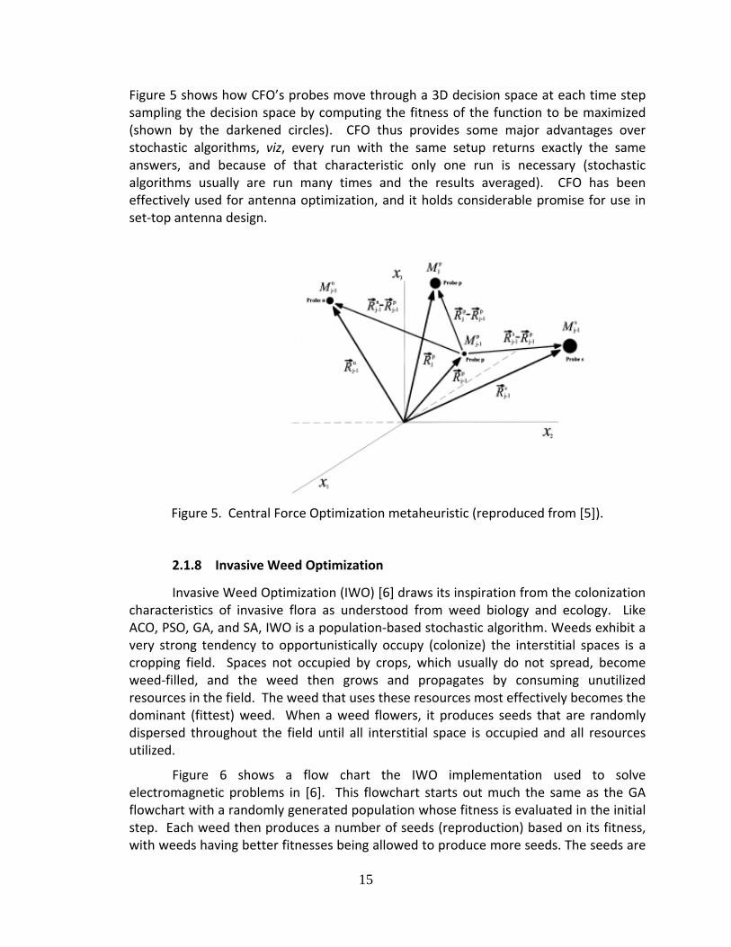
Figure 5 shows how CFO’s probes move through a 3D decision space at each time step sampling the decision space by computing the fitness of the function to be maximized (shown by the darkened circles). CFO thus provides some major advantages over stochastic algorithms, viz, every run with the same setup returns exactly the same answers, and because of that characteristic only one run is necessary (stochastic algorithms usually are run many times and the results averaged). CFO has been effectively used for antenna optimization, and it holds considerable promise for use in set‐top antenna design.
Figure 5. Central Force Optimization metaheuristic (reproduced from [5]).
2.1.8 Invasive Weed Optimization
Invasive Weed Optimization (IWO) [6] draws its inspiration from the colonization characteristics of invasive flora as understood from weed biology and ecology. Like ACO, PSO, GA, and SA, IWO is a population‐based stochastic algorithm. Weeds exhibit a very strong tendency to opportunistically occupy (colonize) the interstitial spaces is a cropping field. Spaces not occupied by crops, which usually do not spread, become weed‐filled, and the weed then grows and propagates by consuming unutilized resources in the field. The weed that uses these resources most effectively becomes the dominant (fittest) weed. When a weed flowers, it produces seeds that are randomly dispersed throughout the field until all interstitial space is occupied and all resources utilized.
Figure 6 shows a flow chart the IWO implementation used to solve electromagnetic problems in [6]. This flowchart starts out much the same as the GA flowchart with a randomly generated population whose fitness is evaluated in the initial step. Each weed then produces a number of seeds (reproduction) based on its fitness, with weeds having better fitnesses being allowed to produce more seeds. The seeds are
16
then randomly dispersed through the decision space using a normal (Gaussian) distribution of random numbers with mean value equal to the weed’s location. After the new seeds have been dispersed, they are allowed to grow into new flowering weeds, and the process is repeated until a convergent solution is generated. Because the number of weeds grows constantly, a maximum weed population serves as a ceiling on weed count. Whenever it is exceeded, the bottom worst plants are “weeded out” by being discarded.
Figure 6. Invasive Weed Optimization flow chart (reproduced from [6]).
2.1.9 Intelligent Water Drop Algorithm
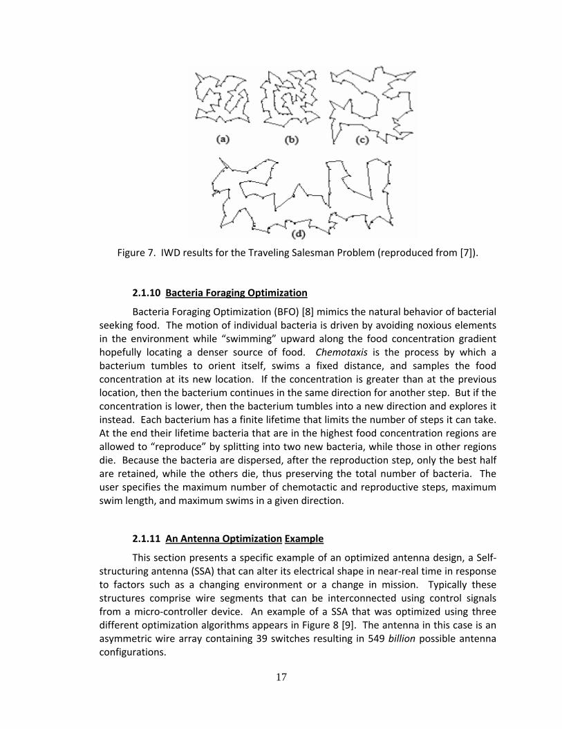
The Intelligent Water Drop algorithm (IWD) [7], like SA and CFO, analogizes a physical process. But, like SA and unlike CFO, it is stochastic in nature instead of deterministic. IWD is inspired by the notion that the seemingly random meanders in a river or stream bed are, in fact, based on mechanisms that can be applied to effectively solve optimization problems. Two principal factors are considered in IWD: water velocity and soil characteristics. Each IWD flows from a source to a destination, initially with non‐zero velocity and zero soil. Along its route, velocity and soil both may be gained and lost. Soil inhibits drop velocity, so that between points the IWD’s velocity increases inversely with soil (in a non‐linear manner). Figure 7 shows typical IWD results for the Travelling Salesman Problem (see also discussion above on SA and TSP).
17
Figure 7. IWD results for the Traveling Salesman Problem (reproduced from [7]).
2.1.10 Bacteria Foraging Optimization
Bacteria Foraging Optimization (BFO) [8] mimics the natural behavior of bacterial seeking food. The motion of individual bacteria is driven by avoiding noxious elements in the environment while “swimming” upward along the food concentration gradient hopefully locating a denser source of food. Chemotaxis is the process by which a bacterium tumbles to orient itself, swims a fixed distance, and samples the food concentration at its new location. If the concentration is greater than at the previous location, then the bacterium continues in the same direction for another step. But if the concentration is lower, then the bacterium tumbles into a new direction and explores it instead. Each bacterium has a finite lifetime that limits the number of steps it can take. At the end their lifetime bacteria that are in the highest food concentration regions are allowed to “reproduce” by splitting into two new bacteria, while those in other regions die. Because the bacteria are dispersed, after the reproduction step, only the best half are retained, while the others die, thus preserving the total number of bacteria. The user specifies the maximum number of chemotactic and reproductive steps, maximum swim length, and maximum swims in a given direction.
2.1.11 An Antenna Optimization Example
This section presents a specific example of an optimized antenna design, a Self‐structuring antenna (SSA) that can alter its electrical shape in near‐real time in response to factors such as a changing environment or a change in mission. Typically these structures comprise wire segments that can be interconnected using control signals from a micro‐controller device. An example of a SSA that was optimized using three different optimization algorithms appears in Figure 8 [9]. The antenna in this case is an asymmetric wire array containing 39 switches resulting in 549 billion possible antenna configurations.
18
The specific problem addressed in [9] was whether or not the optimization algorithms would provide better performance than a simple random search for a configuration that met specific performance criteria.
The wire structure was modeled with the Numerical Electromagnetics Code (NEC) following all modeling guidelines with respect to wire segmentation and segment length to diameter and wavelength ratios. The objective was to obtain low VSWR (< 2) values at frequencies of 40, 100 and 400 MHz. The antenna grid measured 0.6 meter square ( 08.0 on a side at 40 MHz), which electrically is quite small. Figures 8, 9 and 10 compare the results of a random search to those produced by the three optimization algorithms. Random search performed very poorly at the lowest frequency, while each of the optimization algorithms performed relatively well. The GA produced the “tightest” results at 40 MHz (minimum standard deviation), and achieved the design objective in 60% of the trials. This example shows that real‐time‐optimized SSAs are within reach for the set‐top antenna application at this time, and that fairly economical designs may be possible.
Figure 8. SSA geometry (reproduced from [9]).
19
Figure 9. SSA VSWR, random search [left], ACO [right] (reproduced from [9]).
20
Figure 10. SSA VSWR, SA [left], GA [right] (reproduced from [9]).
2.1.12 References
[1] Pechac, P., “Electromagnetic Wave Propagation Modeling Using the Ant Colony Optimization Algorithm,” Radioengineering, 11, No. 3, September 2002, p. 1.
[2] Robinson, J., and Rahmat‐Samii, Y., “Particle Swarm Optimization in Electromagnetics,” IEEE Trans. Antennas and Propagation, 52, no. 2, Feb. 2004, p. 397.
21
[3] Mahanti, G. K., Pathak, N., and Mahanti, P., “Synthesis of Thinned Linear Antenna Arrays with Fixed Sidelobe Level Using Real‐Coded Genetic Algorithm,” Prog. in Electromagnetics Research, PIER 75, 319‐329, 2007.
[4] Kirkpatrick, S., Gelatt, C. D., and Vecchi, M. P., “Optimization by Simulated
Annealing,” Science, 220, no. 4598, 13 May 1983, p. 671.
[5] Formato, R. A., “Central Force Optimization: A New Metaheuristic with Applications in Applied Electromagnetics,” Prog. in Electromagnetics Research, PIER 77, 425‐491, 2007.
[6] Karimkashi, S., and Kishk, A. A., Invasive Weed Optimization and its Features
iElectromagnetics,” IEEE Trans. Antennas and Propagation, 58, no. 4., April 2010,
p. 1269.
[7] Shah‐Hosseini, H., “The Intelligent Water Drops Algorithm: A Nature‐Inspired
Swarm‐ Based Optimization Algorithm,” Int. J. Bio‐Inspired Computation,
1, nos.1/2, p. 71, 2009.
[8] Datta, T., and Misra, I. S., “Adaptive antenna Array Processing: The Bacteria‐
Foraging Algorithm and Particle‐Swarm Optimization,” IEEE Antennas and
Propagation Magazine, 51, no. 6, December 2009, p. 69.
[9] Coleman, C. M., Rothwell, E. J., and Ross, J. e., “Investigation of Simulated
Annealing, Ant‐Colony Optimization, and Genetic Algorithms for Self‐
Structuring Antennas, IEEE Trans. Antennas and Propagation, 52, 4, p. 1007,
April 2004.
22
2.2 Fragmented Antennas
As an additional illustration of the power of an electro‐magnetic (EM) optimization
algorithm, this section describes the computer program FAopt that begins with a grid of
wires as shown in Figures 1 and 2 and optimizes the placement of these wires using a
Binary Genetic Algorithm (BGA) and the NEC‐4 [1] Method of Moments (MoM)
FORTRAN code. Each bit in the BGA chromosome is either a 1 or a 0, representing the
presence or absence of a wire, respectively. Quadrant 1 and 3 are a mirror image of
each other as well as quadrant 2 and 4, so that the antenna is symmetrical about its
diagonal. The resulting antenna is comprised of a series of plated conductors, some of
which are connected to one another. Some are capacitively/inductively coupled and act
as parasitic elements to increase the element impedance and radiation pattern
bandwidth. These types of radiating elements, when implemented as pixels rather than
wires, (see Maloney et al of GTRI [2]) are generally called “fragmented” antennas [3].
FAopt allows the user to choose the polarization as either vertical or horizontal, and the
antenna can be either directional or omni‐directional. The user also can choose the
dimensions for the desired antenna, as well as the frequency range. This program was
used to design a set‐top antenna to operate in the VHF and UHF bands. (See Section
3.0). During optimization a window is shown that updates the progress of the optimizer
with the best “figure of merit” (FoM) displayed along with the standing wave ratio.
Figure 1: FAopt Code’s GUI
23
Figure 2: Wire Grid
As an example, a thin planar directional antenna was optimized using FAopt as a
horizontally polarized antenna from 2400‐2480MHz with 8 blocks per row/column per
quadrant. The orientation appears in Figure 1, and the antenna model is shown in
Figure 3. The dimensions for this antenna are 2” by 2”. A prototype was built as shown
in Figure 4.
Figure 3. Fragmented Directional WiFi Antenna
Figure 4. Fragmented Directional WiFi Antenna
The simulation results, which were confirmed by measurements, shows the average
gain of this antenna to be better than 1.9 dBi. This antenna is a directional WiFi antenna
optimized to have a F/B ratio of about 6 dBi. Its radiation pattern is very consistent
24
across the band as shown in Figure 6, and its measured VSWR is better than 2:1 across
the band. Further work, such as changing the grid template or the optimization routine,
could be undertaken to make this approach more efficient for designing set‐top
VHF/UHF antennas.
Figure 5. Pattern of Directional WiFi Antenna
Figure 6. VSWR of Directional WiFi Antenna
The F/B ratio of simulated and measured are in fair agreement as shown in Figure 7.
Figure 7. F/B Ratio of Directional WiFi Antenna
Directional WiFi Antenna
-2
0
2
4
6
8,+X
10 2030
4050
60
70
80
90
100
110
120130
140150
160170,-X
190200210
220230
240
250
260
270
280
290
300310
320330
340350
2400
2420
2440
2460
2480
VSWR of Directional WiFi Antenna
1
2
3
4
5
6
7
2400 2420 2440 2460 2480
Frequency (MHz)
VS
WR
CalculatedResults
MeauredResults
F/B Ratio of Directional Wifi Antena
0
2
4
6
8
10
2400 2420 2440 2460 2480
Frequency MHz
dB
CalculatedResults
MeasuredResults
25
References
[1] G. J. Burke, “Numerical Electromagnetics Code‐NEC‐4 Method of Moments”, Lawrence Livermore National Laboratory, 1996
[2] J. G. Maloney, M. P. Kesler, P. H. Harms, G. S. Smith, United States Patent No. US 6323809 B1, Nov 27,2001
[3] B. Thors, H. Steyskal and H. Holter, “Broad‐Band Fragmented Aperture Phased Array element Design Using Genetic Algorithms”, IEEE Trans. Antennas Propag., Vol 53, no. 10, pp. 3280‐3287
26
2.3 Non‐Foster Impedance Matching
Foster’s reactance theorem, which dates to 1924, states that a lossless reactance must have
a positive slope with frequency. Any lossless matching network presumably satisfies the
theorem, but a great deal of research that has been done on “non‐Foster matching” in the
past 15 years suggests otherwise. This section examines how non‐Foster networks may be
useful in set‐top antennas to match an electrically small element (characterized by a low
real and high negative imaginary complex impedance) within, for example, the low‐VHF
band.
Until recently no one has created a practical antenna system using this method that showed
much of an improvement in performance. This was due to limitations in the semiconductor
technology at the time that permitted only narrow band solutions. Semiconductor
technology has improved considerably in recent years resulting in increased bandwidth,
lowered noise, and decreased losses in the devices. Electrically small antennas present high
Q impedances characterized by large reactances and small radiation resistances. For such
antennas, the effectiveness of passive matching circuits is severely limited by gain
bandwidth theory, which predicts narrow bandwidths and/or poor gain. The result
inevitably is a poor signal to noise ratio compared with a larger antenna.
Non‐Foster matching uses negative impedance converters (NIC) to create “negative”
capacitors and “negative” inductors [1‐2]. It is possible, for example, to use negative
capacitance to cancel out the reactance in a short dipole or monopole. This leaves only a
small real impedance which could then be matched to, say, 75 Ω using a transformer. One
disadvantage of this approach is that transformers add to the antenna size which could be
undesirable. An alternative to matching could be achieved by placing the non‐Foster
matching circuit away from the feed to control both the real impedance as well as the
reactance of the antenna [3]. The potential improvement in antenna performance is very
significant. Theoretical bandwidth improvements have been shown for a small loop
(increasing bandwidth from 50 MHz to 300MHz at a center frequency of 700MHz), as well
as a small broadband dipole (increasing bandwidth from 250MHz to 1000MHz, lowering the
lower operating frequency from 250 MHz to 190 MHz).
It should be noted that the Figures and Tables in this section were taken from references
2 through 5, listed at the end of this section.
27
Figure 1. Linvill’s ideal OCS NICs terminated in a resistance.
Fiugre 2. Linvill’s ideal SCS NICs terminated in a resistance.
With an ideal transistor, a pure negative resistance is achievable. In Linvill’s actual realizations (Figures 1 and 2), a substantial reactive component of the input impedance Z accompanies the negative resistance, resulting in a low Q, where the “resistive” Q is defined as: Q=Re(Z)/Im(Z). The circuits shown are “open‐circuit stable” (OCS), meaning, practically, that if a very large resistance terminates the negative‐resistance one‐ports on the left, then the overall network will be stable. The networks of Figure 1 can be turned around as shown in Figure 2, where negative resistances of the “short‐circuit stable” (SCS) variety are obtained. Again, practically speaking, this means these networks will be stable if a very large conductance is placed across the input. An initial step in improving the power efficiency of non‐Foster matching is simply to use a single‐transistor version of the NIC [4].
Figure 3. Non Foster Matching
28
An example of a non‐Foster matching circuit is shown in Figure 3. Although not shown in the schematic, a transformer would be used at the input to make the effective value of Rsource, as seen by the matching circuit, to be 18.75Ω (4:1 impedance ratio).The circuit negates antenna’s Capacitance Cant and the voltage‐managing resonating inductor Lres, as well as the radiation resistance r. The idea is to cancel the negated Lres and Cant with C and L on the left, respectively. The negated r is absorbed by the much larger source resistance and does not affect operation of the circuit. The source resistance would be 75 ohms in this case. An example of non‐Foster matching for a 12 inch dipole is shown in Figure 4. It is shown in Figure 5 that this non‐Foster matching network creates a negative capacitance that is used to cancel out the reactance of the 12” dipole. This is used along with a transformer to help match the radiation resistance of the antenna to the source impedance of 50 Ω. The non‐Foster matching network is compared to a similar dipole with a lossy passive network for improvements in signal to noise as shown in Figures 6 and 7. The improvement in SNR is quite remarkable, as much as 25 dB around 44 MHz.
Figure 4. Non‐Foster Matching Network for a 12” Dipole.
Figure 5. Measured and simulated results for capacitance of non‐Foster matching network.
29
Figure 6. Setup for Signal to Noise improvement measurement.
Figure 7. Measured Improvement of Signal to Noise
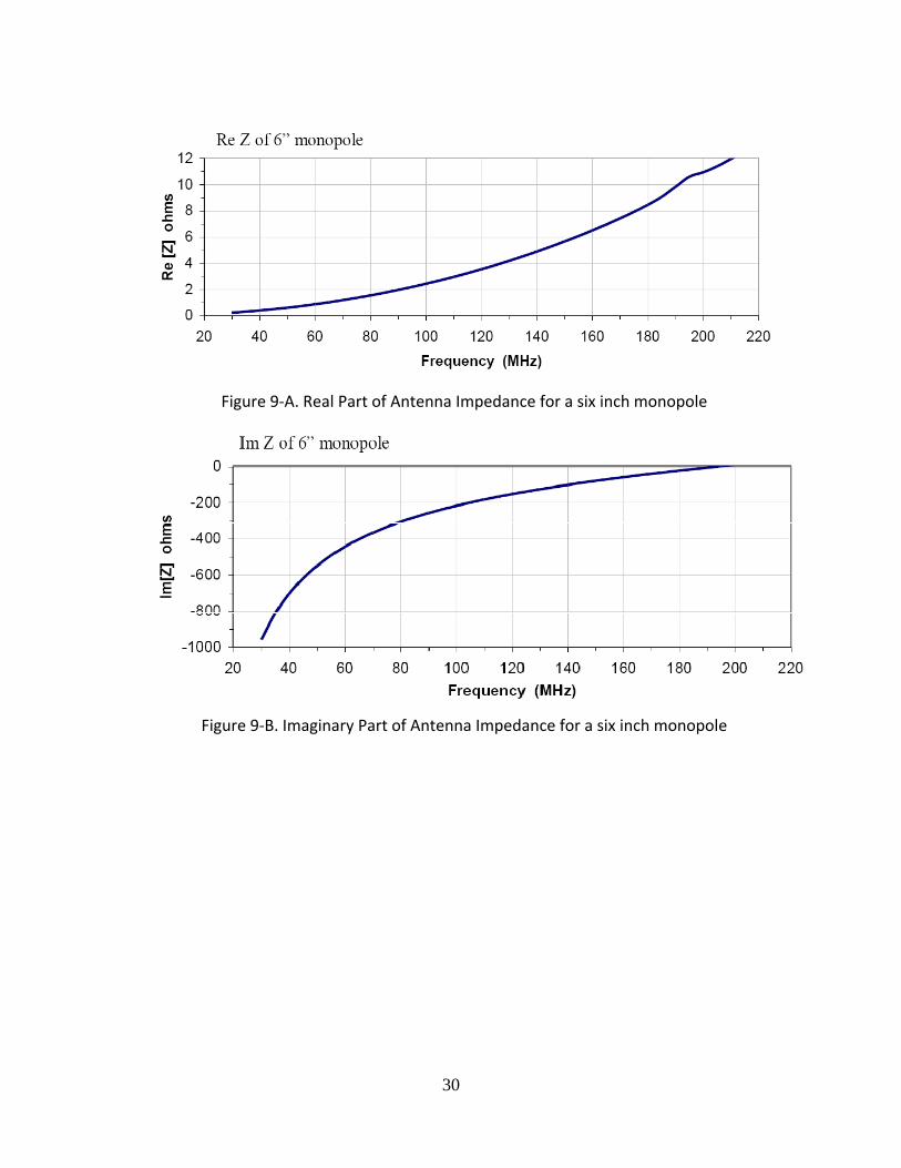
Non‐Foster matching may be particularly useful for the set‐top application because it works best with electrically small antennas. Therefore, this type of match could be useful when designing a small VHF/UHF DTV set‐top antenna. Improvements in signal to noise measurements have been shown from 20MHz to 400 MHz [5]. In particular, the use of non‐Foster techniques to impedance match a lossy electrically‐small dipole antenna has been quite effective. On an antenna range, there was a measured 30 dB gain improvement over 60 – 200 MHz, with several dB of improvement as high as 400 MHz. Again, the comparison was to the same antenna with no matching at all. Although no S/N measurements were made, the circuits used were based upon the same low‐noise designs developed earlier for lower‐frequency circuits. Because of the lossiness of the antenna, passive matching can do a little better than no matching at all, and these results are illustrated in simulation. This computer simulation designed a number of “best‐effort” passive matching networks and calculated the transducer gain (S21) between a 50 ohm source and the complex impedance of a 6‐inch monopole. S21 for no matching and S21 for a single, ideal negative capacitance whose value (‐5.54pF) exactly cancels the antenna reactance at 30 MHz, were calculated. Plots of the real and imaginary parts of the antenna impedance are shown in Figure 8. The various matching networks are illustrated in Figure 9; each of these would appear in place of the NIC in Figure 10b.
30
Figure 9‐A. Real Part of Antenna Impedance for a six inch monopole
Figure 9‐B. Imaginary Part of Antenna Impedance for a six inch monopole
31
Figure 10. Various Matching Techniques for six inch monopole
Table 1. Computed Average Gain of all matching techniques.
32
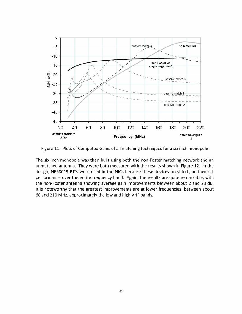
Figure 11. Plots of Computed Gains of all matching techniques for a six inch monopole
The six inch monopole was then built using both the non‐Foster matching network and an unmatched antenna. They were both measured with the results shown in Figure 12. In the design, NE68019 BJTs were used in the NICs because these devices provided good overall performance over the entire frequency band. Again, the results are quite remarkable, with the non‐Foster antenna showing average gain improvements between about 2 and 28 dB. It is noteworthy that the greatest improvements are at lower frequencies, between about 60 and 210 MHz, approximately the low and high VHF bands.
33
Figure 12. Gain of a non‐Foster matching network over the same antenna with no
matching.
Figure 13. Plots of Computed Gains of all matching techniques for a six inch dipole
Results for an electrically small lossy dipole are shown in Figure 13 (this antenna was simulated, not measured). The actual gain may be less due to noise of the device if this were to be built and tested. Thus, realization of non‐Foster technology is still limited by the analog circuitry performance. With respect to the set‐top application, it is very reasonable to expect that as better silicon devices are developed covering the entire television frequency range will be possible with substantially better antenna performance in terms of gain and signal‐to‐noise ratio.
34
References [1] R.C Hansen, “Electrically Small Super directive and Super conducting Antennas”, John Wiley & Sons Inc. 2006 [2] J. T Aberle, R. Leopsinger‐Romak, C. A Balanis, “Antennas with Non‐Foster Matching Networks”, Morgan & Claypool Publishers, 2007 [3] S. Koulouridis and J.L. Volakis, “Non‐Foster circuits for small broadband antennas”, [4] S. E. Sussman‐Fort and R. M. Rudish “Non‐Foster Impedance Matching of Electrically‐ Small Antennas”,IEEE Transactions on Antennas and Prop., Vol 57,NO. 8, August 2009 [5] S. E. Sussman‐Fort and R. M. Rudish, “Non‐Foster impedance matching of a lossy, electrically‐small antenna over an extended frequency range” presented at the Antenna Applicat. Symp., Allerton Park, IL, Sep. 2007
35
2.4 Active RF Noise Cancelling
Considerable work has been done to mitigate noise from devices near receiving antennas, as is particularly useful in set‐top antennas. An antenna placed on top of a television is especially vulnerable because it may pick up noise from internal circuitry. But this noise can be reduced, which in turn reduces the noise floor, or, equivalently, increases the signal‐to‐noise ratio (SNR). Intersil [1] has created the QHx220 chip that accomplishes this e.g. at UHF frequencies, or more precisely from 300 MHz up to >3GHz. MegaWave has evaluated the Intersil noise cancelation chip QHx220 shown in Figure 1. The chip was tested for signal to noise improvements at 535MHz as shown in Figure 2. Measured results showed an improvement of about 12dB in SNR as shown in Figures 3 and 4. This technology has been extended down to FM covering the VHF III band [2], which is necessary for this approach to be viable in the set‐top environment.
This system works on a principle similar to Bose and Sony noise cancelling headsets, but at a ~1,000,000 times higher frequency. It requires an I and Q setting obtained from the DTV receiver’s channel setting and the system’s link quality parameter (BER, SNR, RSSI, etc.). This is done on either a micro‐processor or in the baseband processor, which run a set of small algorithms. As a result the noise minimum is centered in the desired TV channel and signals ‐ formerly buried in the noise floor ‐ are being restored (Figure 4, e.g. at 549MHz).
36
Figure 2 Noise Cancellation Test and Evaluation Setup
Figures 3‐4: Measured results before and after noise cancelation
an electronically tunable microstrip combline filter. These prototype devices point to
LTCC technology’s utility for RF and microwave applications. At this point the new
multilayer architecture proposed in [11] that involves switching between layers for
tuning is being computer‐modeled, but working devices based on that approach have
not been fabricated. LTCC technology may be very attractive in the television frequency
range because of its potential for very high levels of integration resulting from the
multilayer design.
A third example of an on‐chip tracking filter is provided by [12]. A complete
tunable structure was fabricated and tested. This chip occupied an area of only 2.8 mm2
(fabricated with 0.18 μm CMOS) requiring 34‐120 mA at 1.8 VDC. A photomicrograph of
the chip appears in Figure 19, and its architecture in Figure 20. The device comprises
cascaded RLC sections as shown in Figure 20, each containing a digitally programmable
on‐chip capacitor and resistor, and an off‐chip fixed inductor. The resistor is adjusted
with 8‐bit resolution, while the capacitor uses a 10‐bit control signal.
53
Figure 19. Tunable LC‐Tracking filter as fabricated (reproduced from [12]).
Figure 20. Tunable LC‐Tracking filter architecture (reproduced from [12]).
Figure 21 shows the tracking filter’s measured performance data from 125 MHz
to 1.06 GHz. Its response in the 5.6 MHz passband is very flat with a ripple less than 0.2
dB. The noise figure in this device appears to be somewhat high (16.8‐19.5 dB), but the
third‐order intercept points are good (~128/167 dBμV, in/out of band). Frequency
selectivity is good at > 36 dB, and the power consumption quite low (<~0.2 W
maximum). This example shows that very effective single‐chip RF tracking filters with
minimal off‐chip components (in this case two inductors) can be designed and
fabricated for set‐top use using currently available technologies.
54
Figure 21. Measured performance of tunable LC‐Tracking filter (reproduced from [12]).
2.5.1.4 Software Defined Radios
A software defined radio (SDR) is an element of a wireless communication
network whose operational modes and parameters can be changed or augmented post‐
manufacture via software. The essential idea is that a flexible hardware layer exists
whose function can be controlled and modified entirely by a computer program, as
opposed to requiring hardware modifications of any kind. The SDR concept spans many
radio network technologies including cellular systems, personal communications
services (PCS), 3rd and 4th generation wireless (3G and 4G), mobile data, emergency
services, paging, messaging, and military/government communications, and any future
modifications to these existing services or entirely new ones. The FCC (Federal
Communications Commission) definition is more restrictive in that it applies only to the
transmitter side of an SDR. But, as a practical matter, the SDR concept applies to any
wireless device whose characteristics are software‐controllable, whether it be the
transmitter, receiver, both, or some other element such as a modem.
SDR technology is relevant to the television set‐top AT because there is a
developing standard that specifically addresses the issue of “smart antennas” (SAs) in
the context of SDR. This type of antenna and its associated AT may be useful for the set‐
top application and consequently should be monitored as an emerging technology. The
high‐level SDR smart antenna architecture appears in Figure 22. The hardware layer
comprises M transmit antennas and N receive antennas because SDR in general
supports two‐way communication (in the step‐top TV receive application, of course,
there are no transmit antennas). Each antenna is has a separate RF/IF processing chain
with the smart antenna signal processing (“waveform application”) being applied to the
55
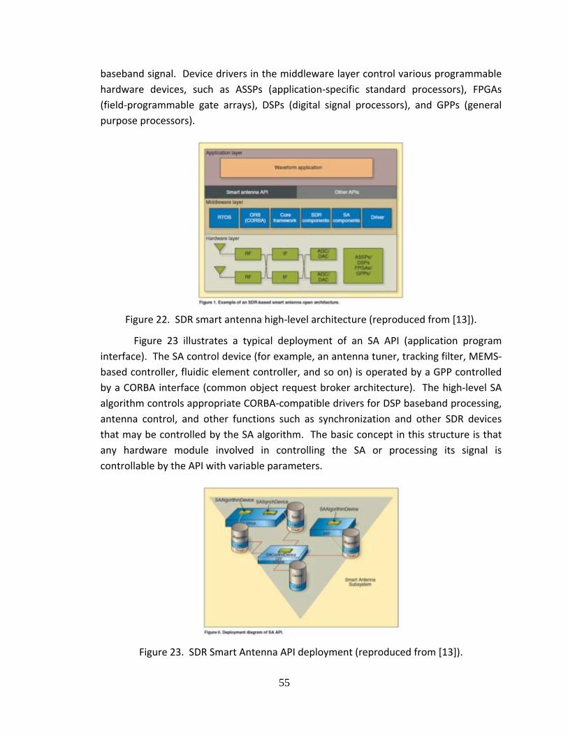
baseband signal. Device drivers in the middleware layer control various programmable
hardware devices, such as ASSPs (application‐specific standard processors), FPGAs
(field‐programmable gate arrays), DSPs (digital signal processors), and GPPs (general
purpose processors).
Figure 22. SDR smart antenna high‐level architecture (reproduced from [13]).
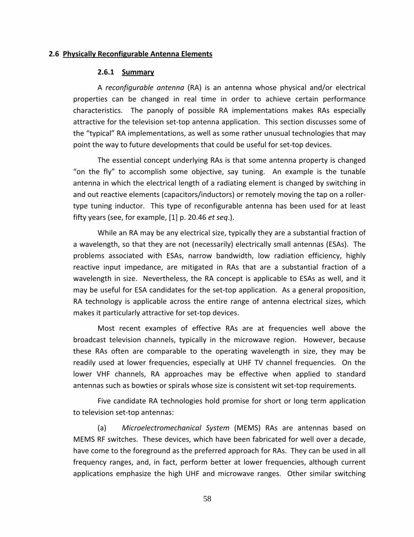
Figure 23 illustrates a typical deployment of an SA API (application program
interface). The SA control device (for example, an antenna tuner, tracking filter, MEMS‐
based controller, fluidic element controller, and so on) is operated by a GPP controlled
by a CORBA interface (common object request broker architecture). The high‐level SA
algorithm controls appropriate CORBA‐compatible drivers for DSP baseband processing,
antenna control, and other functions such as synchronization and other SDR devices
that may be controlled by the SA algorithm. The basic concept in this structure is that
any hardware module involved in controlling the SA or processing its signal is
controllable by the API with variable parameters.
Figure 23. SDR Smart Antenna API deployment (reproduced from [13]).
56
A typical SA hardware implementation for the SDR baseband signal processing
module is shown in Figure 24. The two DSP integrated circuits (ICs), the GPP, and the
FPGA ICs are labeled. This type of module is simply inserted into a backplane containing
the other SDR modules to create a complete SDR. All chip‐level functions are fully
controllable by the SA API. As modifications are required, a simple download of the
updated API is all that is necessary. No hardware modifications or swaps are necessary.
The SDR approach thus provides exceptional flexibility in customizing radio performance
and it well may be a very useful approach to developing effective set‐top television ATs.
Figure 24. Typical SDR smart antenna hardware implementation (reproduced from
[14]).
2.5.2 References
[1] Stemmer, S., “Structure‐Property Relationships of Tunable Thin Film Dielectrics for Microwave Applications,” Ferroelectrics UK Conference, Birmingham, UK, May 23‐26, 2006.
[2] Lee, Y. C., Hong, Y P., and Ko, K. H., “Low‐voltage and High‐tunability Interdigital Capacitors Employing Lead Zinc Niobate Thin Films,” Applied Physics Letters, 90, 182908 (2007).
[3] Peregrine Semiconductor Corp., 9380 Carroll Park Drive, San Diego, CA 92121 USA (www.psemi.com).
[4] Ranta, T., and Novak, R., “Antenna Tuning Approach Aids Cellular Handsets,” Microwaves & RF, p. 82, November, 2008.
57
[5] Soulimane, S., Casset, F., Chapuis, F., Charvet, P. L., and Aid, M., “Tuneable
Capacitor based on Dual Picks Profile of the Sacrificial Layer,” DTIP of MEMS
DTIP of MEMS & MOEMS, Stresa, Italy, 25‐27 April 2007 (EDA
Publishing/DTIP 2007, ISBN: 978‐2‐35500‐000‐3).
[9] Firrao, E. L., Annema, A‐J., Nauta, B., “An Automatic Antenna Tuning System
Using only RF Signal Amplitudes,” IEEE Trans. Circuits and Systems – II:
Express Briefs, 55, No. 9, pp. 833‐837, Sept. 2008.
[10] Sun, Y., Lee, J‐s., Lee, S‐g., “On‐chip Active RF Tracking Filter with 60dB 3rd‐ Order Harmonic Rejection for Digital TV Tuners,” SoC Design Conference, 2008. ISOCC '08, 24‐25 Nov. 2008, Busan, vol. 01, pp I_406‐I_409. DOI: 10.1109/SOCDC.2008.4815658
[11] Suma, M. N., and Suhas, K., “Performance Analysis and Process Parameters of Novel LTCC Filters,” International Journal of Recent Trends in Engineering, 1, No. 3, p. 346, May 2009.
[13] Hyun, S., Kim, J., Choi, S., Pucker, L., Fette, B., “Standardizing Smart Antenna API for SDR Networks,” RF Design, p. 34, Sept. 2007.
[14] Hyeon, S., kim, J., Choi, S., “Smart Antenna APIS: From Concept to Practice,”
Proc. SDR 07 Technical Conference and Product Exposition, SDR Forum,
http://www.wirelessinnovation.org
58
2.6 Physically Reconfigurable Antenna Elements
2.6.1 Summary
A reconfigurable antenna (RA) is an antenna whose physical and/or electrical
properties can be changed in real time in order to achieve certain performance
characteristics. The panoply of possible RA implementations makes RAs especially
attractive for the television set‐top antenna application. This section discusses some of
the “typical” RA implementations, as well as some rather unusual technologies that may
point the way to future developments that could be useful for set‐top devices.
The essential concept underlying RAs is that some antenna property is changed
“on the fly” to accomplish some objective, say tuning. An example is the tunable
antenna in which the electrical length of a radiating element is changed by switching in
and out reactive elements (capacitors/inductors) or remotely moving the tap on a roller‐
type tuning inductor. This type of reconfigurable antenna has been used for at least
fifty years (see, for example, [1] p. 20.46 et seq.).
While an RA may be any electrical size, typically they are a substantial fraction of
a wavelength, so that they are not (necessarily) electrically small antennas (ESAs). The
problems associated with ESAs, narrow bandwidth, low radiation efficiency, highly
reactive input impedance, are mitigated in RAs that are a substantial fraction of a
wavelength in size. Nevertheless, the RA concept is applicable to ESAs as well, and it
may be useful for ESA candidates for the set‐top application. As a general proposition,
RA technology is applicable across the entire range of antenna electrical sizes, which
makes it particularly attractive for set‐top devices.
Most recent examples of effective RAs are at frequencies well above the
broadcast television channels, typically in the microwave region. However, because
these RAs often are comparable to the operating wavelength in size, they may be
readily used at lower frequencies, especially at UHF TV channel frequencies. On the
lower VHF channels, RA approaches may be effective when applied to standard
antennas such as bowties or spirals whose size is consistent wit set‐top requirements.
Five candidate RA technologies hold promise for short or long term application
to television set‐top antennas:
(a) Microelectromechanical System (MEMS) RAs are antennas based on
MEMS RF switches. These devices, which have been fabricated for well over a decade,
have come to the foreground as the preferred approach for RAs. They can be used in all
frequency ranges, and, in fact, perform better at lower frequencies, although current
applications emphasize the high UHF and microwave ranges. Other similar switching
59
devices such as PIN diodes or GaAs (gallium arsenide) solid‐state switches also are used
to build RAs, but these technologies are older and perform less well. The latest
developments in MEMS, nano‐MEMS and the use of carbon nano‐tubes (CNT), reduce
sizes and improve performance to the point where there seems essentially no question
that MEMS‐based set‐top RAs will be achievable in the near future.
(b) Fluidic RAs are a very recent development that promises simple, cost‐
effective, rugged reconfigurable wire antenna structures in almost any shape
imaginable. Fluidic elements are fabricated from a flexible eslastomer enclosing human‐
hair‐thin channels filled with eutectic gallium/indium (EGaln), a liquid metal. The
resulting “wire” provides electrical performance similar to copper and can be stretched,
bent, rolled, or twisted into almost any shape simply by applying mechanical stress. The
wire returns to its original linear structure upon relieving the stress. These elements
have been used to fabricate a simple center‐fed dipole that is tuned by stretching. A
similar approach using a multiplicity of wires or other geometries (for example, bow ties
or spirals) may well be the basis of a simple, effective set‐top antenna. This technology
has only recently been reported, and it certainly bears watching as a candidate for set‐
top RAs.
(c) Pixelated piston RAs comprise small individually controllable and
addressable “pistons” in a two‐dimensional matrix. Each piston is controlled by an
actuator which, in turn, is operated by an electronic controller. A conductive patch is
mounted on the end of each piston, which in their quiescent position form a continuous,
flat ground plane. Each piston moves back and forth above and below the ground
plane to form reconfigurable antenna radiating elements or transmission lines. This
technology, which is patented, has been demonstrated to provide high‐gain, beam
steerable, antennas operating from 500 MHz to 18 GHz with reconfiguration times less
than one millisecond. Its utility for the set‐top application is self‐evident, but at this
point in its development the cost likely is prohibitive.
(d) Liquid crystal (LC) RAs are fabricated using LC substrates sandwiched
between two electrodes that apply a DC bias voltage to control the LC’s dielectric
constant by deforming its molecules. Very small unit cells are fabricated that can be
formed or applied onto surfaces of various shapes. At this point in its development, LC
RAs have been demonstrated only on planar surfaces, and only at extremely high
frequencies (high microwave through millimeter wave ranges). An effective LC RA
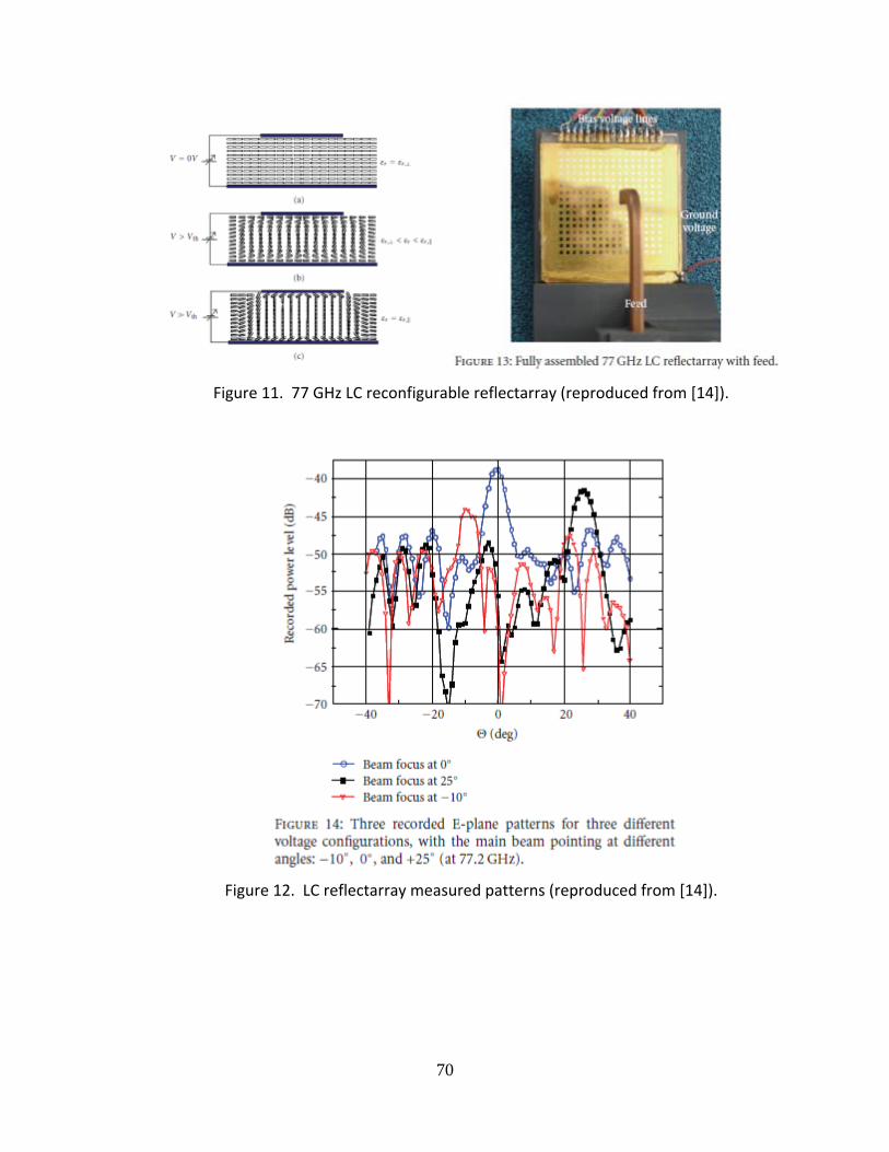
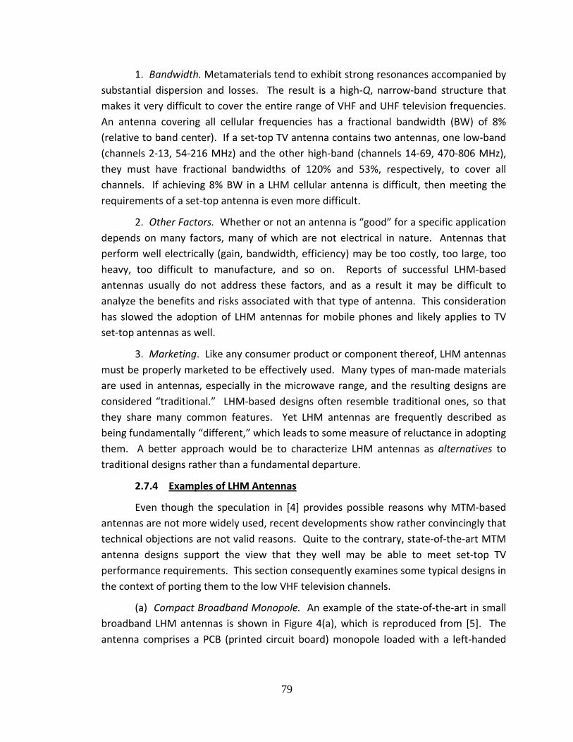
reflectarray antenna has been demonstrated at 77 GHz. It provided complete electronic
beam steering over an angular range of 35 degrees with good gain and sidelobe
performance. Whether or not this technology can be ported to low VHF television set‐
60
top channels is not clear, but the technology bears watching because it is demonstrably
effective for designing and building reconfigurable antennas.
(e) Plasma RAs are similar to the pixilated piston antennas, but instead of
using conductive patches, they utilize ionized gas (plasma) as the conductive element.
Each plasma element is turned “on” (ionized) or “off” (non‐conducting) by a control
voltage, so that the entire antenna aperture is electronically reconfigurable. Unlike
pixilated piston RAs, the plasma elements lie in a single plane and cannot be positioned
above or below the plane. This limitation, however, is minor in the context of set‐top
receive antennas because it is very likely that good receiving structures can be formed
on a planar surface, which also simplifies the RA. The plasma RA has another potentially
significant advantage over other candidate technologies. Existing plasma display
technology, which is very highly developed and sophisticated, may be directly applicable
to the design and manufacture of plasma RAs for the set‐top application. Leveraging
this existing technology may speed time to market and reduce costs substantially.
2.6.2 MEMS‐based RAs
Microelectromechanical system (MEMS) radio‐frequency switches have gained
widespread acceptance as a standard element for implementing in RA structures. RF
MEMS are routinely used to change both antenna feed networks to accomplish
impedance matching and radiating element topology to control radiation pattern and
efficiency. Most applications are in the microwave range, but MEMS use is not
frequency‐limited.
While there are other switching elements besides MEMS, notably sold‐state PIN
diodes and GaAs switches, MEMS offer several advantages. They are inexpensive, which
is a major advantage for set‐top applications, and they exhibit low insertion loss and low
power consumption [2]. In recent years their availability as a commercial item has
grown considerably, and they are now readily available as off‐the‐shelf components
[3,4,5]. Demonstrated lifetimes exceed 100 billion cycles, which is consistent with
consumer levels of usage over periods of several years.
Figure 1 shows a typical bi‐layer curled MEMS structure. It is extremely small in
size (300x1500μm). The two‐layer switch element comprises materials with different
thermal coefficients of expansion that pull it up away from the contact after annealing
as shown in (a). The switch therefore is normally open (NO) when no control voltage is
applied. Applying a DC voltage between the switch post and bottom electrode (1.5 μm
thick polysilicon) creates an electrostatic field that pulls the switch element onto the
contact as shown in (b). The microphotograph below the switch diagram shows its
structure as actually fabricated.
61
Figure 1. Typical RF MEMS switch (reproduced from [2]).
MEMS technology is improving at a rapid pace, and the latest generation of
these switches are nano‐scale [6]. Nanoelectromechanical system (NEMS) are laterally
~10‐100 times smaller than a typical MEMS device, and they operate with actuation
voltages below 10 volts, compared to 30‐80 volts for MEMS switches. NEMS also
provide faster switching times (<~1 μsec) compared to MEMS (~10‐20 μsec ). Figure 2
shows the new NEMS double‐arm cantilevered switch schematically (a) and as
fabricated (b) imaged by a scanning electron microscope.
62
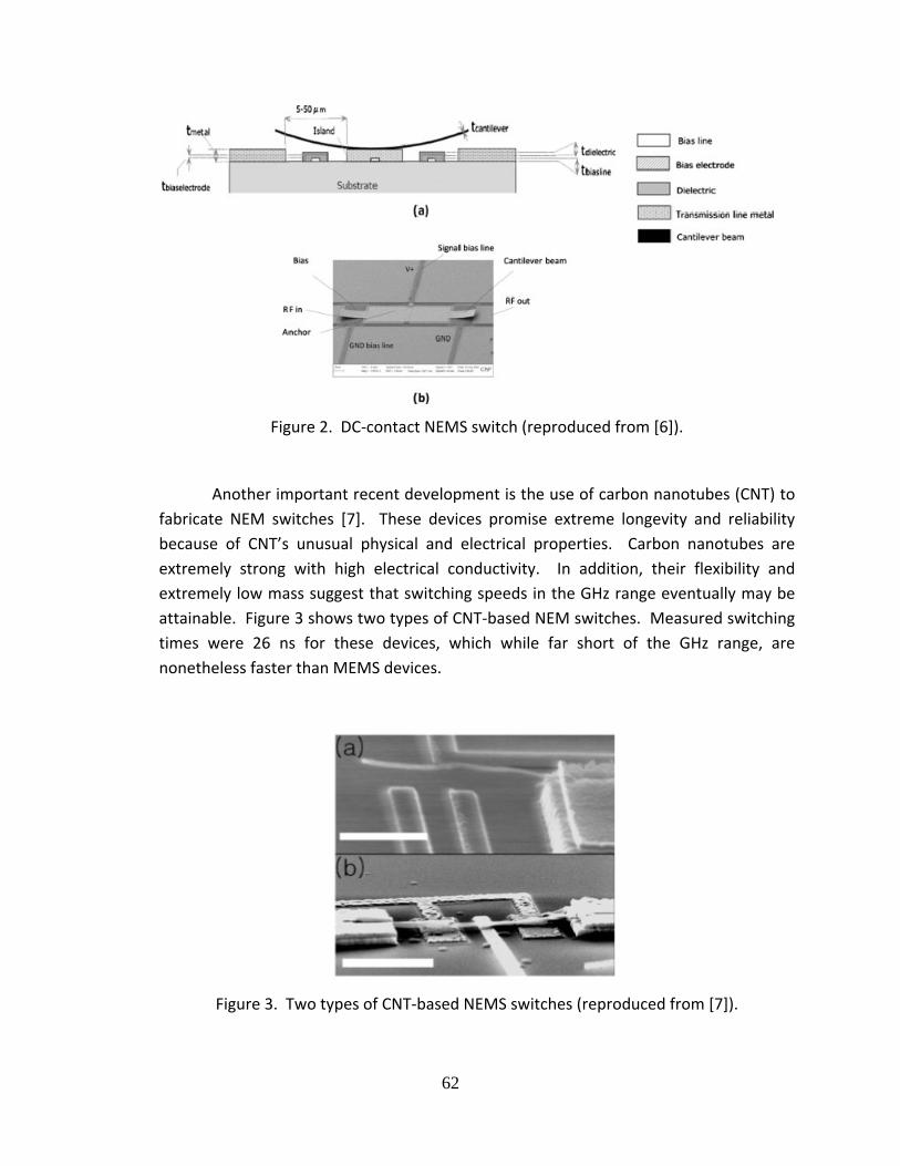
Figure 2. DC‐contact NEMS switch (reproduced from [6]).
Another important recent development is the use of carbon nanotubes (CNT) to
fabricate NEM switches [7]. These devices promise extreme longevity and reliability
because of CNT’s unusual physical and electrical properties. Carbon nanotubes are
extremely strong with high electrical conductivity. In addition, their flexibility and
extremely low mass suggest that switching speeds in the GHz range eventually may be
attainable. Figure 3 shows two types of CNT‐based NEM switches. Measured switching
times were 26 ns for these devices, which while far short of the GHz range, are
nonetheless faster than MEMS devices.
Figure 3. Two types of CNT‐based NEMS switches (reproduced from [7]).
63
A typical MEMS‐based reconfigurable array structure appears in Figure 4. This is
an example of a complex RECAP (Reconfigurable Aperture) structure whose objective is
wide bandwidth. Because a MEMS‐based antenna can be reconfigured essentially in
real‐time, it can operate in multiple frequency bands. Aperture reconfiguration is
achieved by switching in and out receiving and/or transmitting elements (radiating a
signal, of course, is not an issue with set‐top TV antennas). The structure shown in
Figure 4 typically would be implemented using solid‐state switches, but MEMS
technology has leap‐frogged that approach, so that MEMS provides better performance.
In the array application, only the MEMS network departs from an otherwise standard
design. The receiving/radiating element structure and its feed network are independent
of the MEMS switch layer, as are the bias, FSS (frequency selective surface) and PBG
(photonic band gap) layers. These last two elements may well not be required in an
application like the set‐top antenna because the operating frequencies are well below
the microwave range where FSS and PBG structures are common.
Figure 4. Reconfigurable MEMS‐based antenna array (reproduced from [8]).
Another example of a state‐of‐the‐art multiband MEMS‐based antenna is
reported in [9]. The design emphasizes a symmetric, repeatable topology which lends
itself well to scalability, so that additional frequency bands are readily added. Scalability
could be an important attribute in applying MEMS technology to the set‐top
environment, and this antenna demonstrates that scalability is achievable with MEMS.
As configured the antenna covers four bands: 800‐900 MHz; 1.7‐2.5 GHz; 3.3‐3.6 GHz;
and 5.1‐5.9 GHz. The lowest band lies just above the highest UHF television range,
suggesting that this design likely could be easily modified to cover some portion of the
upper TV channels. Table 2 reproduced below from [9] shows that this antenna indeed
provides excellent performance in the four design bands. Its structure appears in Figure
5.
64
Figure 5. Four band MEMS‐based antenna (reproduced from [9]).
2.6.3 Fluidic RAs
An interesting new RA technology is the fluidic antenna. A fluid metallic alloy, eutectic gallium/indium (EGaln), comprising the metals gallium and indium, that remains liquid room temperature is injected into a microfluidic channel made from the silicone elastomer PDMS (polydimethylsiloxane). The channels are very small, about the width of a human hair, open at each end, and of any desired shape. After the channel is filled with EGaln, the alloy’s surface oxidizes, creating a “skin” that holds the alloy in place while allowing it to retain its liquid properties. The alloy’s mechanical properties are determined by the elastomer casing because it remains liquid.
The “wires” created by this process can be bent, stretched, rolled and twisted by applying a stress. Figure 6 shows a photograph of a twisted fluidic wire. Upon relieving the stress, the liquid conductor/elastomer reversibly returns to its original shape without hysteresis. An antenna fabricated of fluidic elements consequently is fully reconfigurable. The structure is self‐healing to small cuts, and it is highly flexible and durable. Life expectancy therefore is very high, and fabrication costs reasonable because the elastomer’s channels are formed using a technique known as “soft lithography” which avoids milling or etching in fabricating the fluidic antenna elements. However, the EGaln liquid metal is expensive, and at this time may be prohibitive for consumer applications.
65
A simple center‐fed dipole was constructed from the fluidic element and tested. The antenna is shown in Figure 7. Its radiation efficiency was measured at approximately 90% over a frequency range of 1910‐1990 MHz tuned by stretching the antenna. The efficiency is comparable to a copper element in this frequency range, so that the fluidic antenna is expected to perform as well as any metallic structure. In the television set‐top application, this type of RA may be very attractive, especially if the price of EGaln alloy can be reduced because of volume. Of course, there are unanswered questions, for example, to what degree the elastomer casing can be stretched. The important conclusion that can be drawn from the reported research is that an entirely new fluidic technology may be close enough to maturity that it soon will be viable for reconfigurable set‐top receive antennas.
Figure 6. Twisted fluidic wire element.
Figure 7 (a. b, c) Photographs of a prototype antenna being stretched and rolled. There
is no hysteresis in the spectral properties of the antenna as it is returned to the
‘‘relaxed’’ state. d) The antenna self‐heals in response to sharp cuts, such as those
inflicted by a razor blade. Fluidic dipole antenna (reproduced from [10]).
66
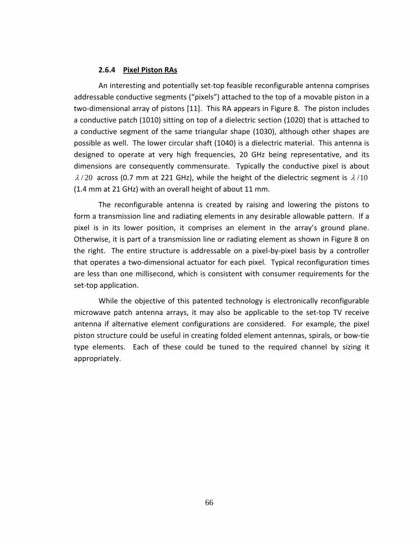
2.6.4 Pixel Piston RAs
An interesting and potentially set‐top feasible reconfigurable antenna comprises
addressable conductive segments (“pixels”) attached to the top of a movable piston in a
two‐dimensional array of pistons [11]. This RA appears in Figure 8. The piston includes
a conductive patch (1010) sitting on top of a dielectric section (1020) that is attached to
a conductive segment of the same triangular shape (1030), although other shapes are
possible as well. The lower circular shaft (1040) is a dielectric material. This antenna is
designed to operate at very high frequencies, 20 GHz being representative, and its
dimensions are consequently commensurate. Typically the conductive pixel is about
20/ across (0.7 mm at 221 GHz), while the height of the dielectric segment is 10/
(1.4 mm at 21 GHz) with an overall height of about 11 mm.
The reconfigurable antenna is created by raising and lowering the pistons to
form a transmission line and radiating elements in any desirable allowable pattern. If a
pixel is in its lower position, it comprises an element in the array’s ground plane.
Otherwise, it is part of a transmission line or radiating element as shown in Figure 8 on
the right. The entire structure is addressable on a pixel‐by‐pixel basis by a controller
that operates a two‐dimensional actuator for each pixel. Typical reconfiguration times
are less than one millisecond, which is consistent with consumer requirements for the
set‐top application.
While the objective of this patented technology is electronically reconfigurable
microwave patch antenna arrays, it may also be applicable to the set‐top TV receive
antenna if alternative element configurations are considered. For example, the pixel
piston structure could be useful in creating folded element antennas, spirals, or bow‐tie
type elements. Each of these could be tuned to the required channel by sizing it
appropriately.
67
Figure 8. Pixel piston reconfigurable array (reproduced from [11]).
This technology has been implemented in commercially available antennas [12].
PARCA (Pixel‐Addressable Reconfigurable Conformal Antenna) arrays are being
developed for military applications requiring UWB (ultra wide‐band) transmit antennas
that adaptively reconfigure operating frequency, gain (beam width), and polarization
while handling high power (~2 KW). A typical implementation operating from 1 to 18
GHz using approximately 100,000 ~1.65 mm diameter pixels would be 0.5 meter (20.5
in) square in size with a thickness of about 20 mm (0.8 in). Approximate weight is 12
lbs. This PARCA array would provide gain of 15 dBi and 40 dBi at 1 GHz and 18 GHz,
respectively. The antenna is shown schematically in Figure 9.
Testing of microstrip transmission line and patch pixelated antennas has been
done with good performance being demonstrated from 500 MHz to 18 GHz [13].
Whether or not this technology can be extended an order or magnitude lower in
frequency for the set‐top application with reasonable overall size is an open question.
But it is clear from the current state‐of‐the‐art that pixilated RAs constitute a technology
to watch for the set‐top receive antenna.
68
Figure 9. UWB PARCA array (reproduced from [13]).
2.6.5 Liquid Crystal Reconfigurable Antennas
Liquid crystal (LC) technology has recently been applied to RF front end
components and array antennas for satellite applications, typically at quite high
frequencies (> 20 GHz). Porting this technology to the low VHF range for a television
set‐top receive antenna simply may not be possible. Nevertheless, LC technology is
worth monitoring because it may migrate to substantially lower frequencies, or it may
inspire development of similar crystal‐based technologies that are applicable in the VHF
range.
Liquid crystals are inherently anisotropic and are so named because they
simultaneously exhibit properties of liquid and crystalline materials. The class of
nematic LCs provide the best dielectric characteristics from the microwave through
millimeter wave bands, and therefore are the material of choice for very short
wavelength RAs. A nematic LC molecule has a more or less rod‐like shape a shown in
Figure 10. Anisotropy is reflected in different perpendicular and parallel (relative to an
incident electric field) dielectric constants, typical values being ~2.5 and ~2.8‐3.5,
respectively. Application of a bias voltage to an LC causes a deformation of the
molecular alignment as shown schematically in Figure 10, the effect of which is to
change the LC’s dielectric properties. These changes, in turn, constitute the basis of a
reconfigurable antenna element.
69
Figure 10. LC deformation modes (reproduced from [14]).
A reflectarray RA was fabricated using a dielectric substrate whose properties
could be tuned using a bias voltage less than about 20 volts. The RA is a waveguide‐fed
planar reflecting surface capable of accurately steering the radiated beam into a wide
range of directions. A unit cell comprising a single microstrip patch of dielectric
sandwiched between two parallel plate electrodes is shown in cross‐section in Figure 7
(left). The upper electrode patch is printed onto the dielectric substrate as is the lower
electrode which acts as the antenna’s ground plane. Initial LC molecule alignment is
achieved using a thin (~300 nm) polyimide film on the electrode patch and ground
plane. The applied external electric field created by the bias voltage reorients the LC
molecules, thereby changing its dielectric properties. The figure shows the variation of
dielectric constant as the bias voltage increases from zero to a value slightly exceeding
the LC’s threshold voltage, thV , and then to a value that is much greater. As the
effective dielectric constant changes, so does the capacitance per unit length of the
microstrip patch, which allows the cell to be voltage‐tunable as a reconfigurable
antenna element.
The reflectarray antenna comprises 16x16 unit cells spaced 55.0 . Each cell is
2.2 mm across with an LC cavity height of 50 μm. The complete antenna is shown in
Figure 11, in which the individual cells are clearly visible, as are the control lines (bias
lines). The antenna is fed using a right‐angle bent WR‐10 open‐ended waveguide as
shown in the figure. Figure 12 shows measured pattern data for different bias voltage
levels. The main lobe is clearly steered into the desired directions of zero (blue), +25
(black), and ‐10 (red) degrees with good relative main lobe gain and sidelobe
suppression.
70
Figure 11. 77 GHz LC reconfigurable reflectarray (reproduced from [14]).
Figure 12. LC reflectarray measured patterns (reproduced from [14]).
71
2.6.6 Plasma Reconfigurable Antennas
The plasma RA [15] is conceptually similar to the PARCA antenna in §4. It also
uses electrically conductive/non‐conductive surfaces to create radiating elements and
associated components. But instead of conductive metallic patches, the plasma RA
utilizes gas enclosures in which the gas can be made electrically conductive (plasma
state) or non‐conductive. The enclosures are interconnected and can be turned on
(conducting) and off (non‐conducting) by applying a control voltage. Figure 13 shows
the basic plasma RA structure. It comprises square cells that contain four control
electrodes, one on each edge. In the diagram, a cell that is turned on is shown by wavy
lines between the electrodes. For example, cell 110 is “on” as shown by the wavy lines
which indicate that the gas within the cell has been ionized into a plasma state. By
contrast, cell 202 is “off” as indicated by the absence of wavy lines; its gaseous contents
have not been ionized. Turning individual cells on and off in the manner forms the basis
for a reconfigurable antenna system.
Figure 13. Plasma RA structure (reproduced from [15]).
While the reconfigurable aperture in Figure 13 can be used on a stand‐alone
basis, it frequently is coupled to backplane as shown in Figure 14. The backplane
comprises control elements (304) that are arrayed on an insulating substrate (302) with
conductive traces (312) that form the control lines. When mated with the plasma
structure, the control elements turn individual gas enclosures on and off. A typical
72
complete plasma RA is shown in Figure 15, which adds a ground plane (404) printed on a
dielectric substrate (402). The sandwich comprising the individually controllable plasma
enclosures, the groundplane, and the backplane form an electronically reconfigurable
antenna system.
The plasma RA may be particularly useful as a set‐top antenna. One advantage is
has over other approaches is that it almost certainly can benefit from the highly
developed plasma screen technology used in consumer televisions. A plasma RA should
be much simpler in structure and fabrication than a large plasma screen display.
Applying existing display technology to manufacturing plasma RAs may be only an
incremental step, thereby reducing time to market and costs.
Figure 14. Plasma RA backplane (reproduced from [15]).
Figure 15. Complete plasma RA (reproduced from [15]).
73
2.6.7 References
[1] Reed, D. (ed.), The ARRL Handbook (2004), American Radio Relay League, Newington, CT 06111 USA.
[2] Ativanichayaphong, T., Cai, Y., Wang, J., Chiao, M., and Chiao, J.‐C., “Design Considerations of Reconfigurable Antennas using MEMS Switches,” SPOIE 2005 Microelectronics, MEMS, and Nanotechnology Symposium, Brisbane, Australia, Dec. 11‐15, 2005.
[3] RadantMEMS, Inc., 255 Hudson Road, Stow, MA 01775 USA.
[4] DowKey Microwave Corp., 4822 McGrath Street, Ventura, CA 93003 USA.
[5] MEMScomm, LLC, 419r East Main Street, Morehead, KY 40351 USA.
[6] Cetiner, B., Biyikli, N., Yildirim, B. S., and Damgaci, “Nanoelectromechanical
Switches for Reconfigurable Antennas,” Microwave and Optical Technology
Letters, 52, No. 1, January 2010.
[7] Lee, S., Eriksson, A., Abdelrahim, A. S., Campbell, E. E. B., “Carbon‐nanotube‐
based Nano Electromechanical Switches,” Jour. Korean Physical Society, 55, No.
3, pp. 957‐961, Sept. 2009.
[8] Sabel, K. F., Katehi, L. P. B., Sarabandi, K., “Modeling and Design of MEMS‐
Based Reconfigurable Antenna Arrays,” IEEE Aerospace Conference, 2003.
Proceedings, p. 2‐1135. DOI: 10.1109/AERO.2003.1235528
[9] Wu, T., Li, R. L., Eom, S. Y., Lim, K., Jeon, S. I., Laskar, J., and Tentzeris, M. M.,
“A Multiband/Scalable Reconfigurable Antenna for Cognitive Radio Base
Stations,” IEEE Antennas and Propagation Society International Symposium,
2008. AP‐S 2008, 5‐11 July 2008, pp. 1‐4. DOI: 10.1109/APS.2008.4619490.
[10] So, J‐H., Thelen, J., Qusba, A., Hayes, G. J., and Dickey, M. D., “Reversibly Deformable and Mechanically Tunable Fluidic Antennas, ” Advanced Functional Materials, 19, pp. 3632‐3637 (2009). DOI: 10.1002/adfm.200900604.
[11] Walton, et al., “Reconfigurable Antenna Using Addressable Pixel Pistons,” U.S. Patent No. 7,561,109 B2, July 14, 2009.
[12] Syntonics, LLC, 9160 Red Branch Road, Columbia, MD 21045 USA.
[13] Syntonics, http://www.syntonicscorp.com/
[14] Gaebler, A., Moessinger, A., Goelden, F., Manabe, A., Goebel, M., Follmann, R.,
Koether, D., Modes, C., Kipka, A,. Deckelmann, M., Rabe, T., Schulz, B.,
Kuchenbecker, P., Lapanik, A., Mueller, S., Haase, W., and Jakoby. R., “Liquid
Crystal‐Reconfigurable Antenna Concepts for Space Applications at Microwave
74
and MillimeterWaves,” International Journal of Antennas and Propagation,
Volume 2009, Article ID 876989, 7 pp. DOI:10.1155/2009/876989.
[15] Metz, C., “Reconfigurable Plasma Antenna with Interconnected Gas Enclosures,”
U.S. Patent Application Publication No. US 2006/0220980 A1, Oct. 5, 2006.
75
2.7 Use of Metamaterials in Antenna Systems
2.7.1 Summary
Traditional antennas are fabricated from electrical conductors such as copper or
aluminum and insulators such as plastic or rubber. Their performance is limited by their
electrical size, that is, the largest dimension measured in wavelengths. Electrically small
antennas are narrow‐band, inefficient, and difficult to impedance‐match. The demands
on a television set‐top antenna are for the most part antithetical. It must be small, but
it requires a very wide bandwidth to cover all VHF/UHF broadcast channels with good
gain and efficiency. Traditional antennas therefore have fallen short of providing good
set‐top performance.
A very promising emerging technology that may soon well address this limitation
is the use of metamaterials (MTM) in the set‐top antenna. This section examines
whether or not MTM can sufficiently improve the performance of electrically small
antennas to make MTM‐based designs attractive for set‐top use. While MTM have been
available since the mid‐1990s and the subject of much literature, they have not gained
widespread commercial acceptance until recently. A recent survey paper examines this
question and suggests some explanations for the MTM’s slow acceptance, much of
which is not based on the technology itself.
More recent developments show that well‐designed MTM‐based antennas
indeed can provide significantly improved performance over traditional designs, but the
reported designs are in frequency bands well above the TV VHF band. Wireless
communication antennas have been designed, fabricated, and measured that improve
on the “Chu limit” for small antenna performance by orders of magnitude using MTM.
Substantially improved bandwidth, high efficiency, and good gain are available from
antennas with maximum dimensions less than one‐tenth wavelength. The question is
whether or not this technology can be ported to the low end of the television broadcast
band; and, while the answer is not guaranteed, it appears to be in the affirmative.
The MTM‐based antenna is an attractive candidate for the set‐top application,
and it should be vigorously studied as a candidate architecture. Because MTM typically
are formed from simple wire structures, they likely can be optimized for the set‐top
application, which may lead to designs that are different than those used at higher
frequencies that still meet set‐top performance objectives.
76
2.7.2 What is a metamaterial?
The term metamaterial (MTM) applied to antennas does not connote a material
in its commonly used sense. The materials used to fabricate an antenna broadly fall into
the categories of conductors (metallic elements), insulators (non‐conductors), and,
occasionally, semiconductors. Materials like copper, aluminum, silver, various plastics,
rubber, paper, and so on, are what come to mind as typical antenna materials; and all of
these share some common features. Whether naturally occurring or man‐made, they
are homogeneous with electrical properties determined by their chemical structure.
Like all other naturally occurring substances (at least all that are known at this time),
(b) Efficient Electrically Small Antenna (EESA). An MTM‐based Efficient Electrical
Small Antenna (ESSA) [6] is shown in Figure 5. It provides another example of how LHM
antennas can achieve performance that is not possible with traditional designs, and
suggests that porting MTM designs to TV set‐top antennas is a viable approach to
achieving improved performance.
The ESSA comprises a monopole surrounded by an SNG (single negative) MTM
structure mounted on a plane substrate. It achieves a voltage standing wave (VSWR)
bandwidth 2 of 470 MHz (1.75‐2.22 GHz) [fractional VSWR bandwidth of 24%] in a
package with an electrical size of only 07.0 . The addition of LHM in this case resulted
in a much broader bandwidth than could achieved otherwise because the effect MTM’s
effect is to lower the system Q‐factor from the theoretical “Chu limit” of 16.72 for
traditional materials to 2.23. Significantly, the increased bandwidth is not accomplished
at the expense of radiation efficiency or gain, which often must be sacrificed in
traditional designs. The ESSA’s measured maximum gain and efficiency were 2.44 dBi
and 83.61%, respectively.
The radiation patterns generally exhibited broad lobes with fairly shallow nulls (
dB25 , Figure 6), which lend themselves well to omnidirectional reception as
required in a set‐top antenna. Because the ESSA’s electrical size is comparable to that
required for a set‐top antenna (see §3), it may be possible to “stack” several ESSA’s
covering different band segments in a fairly small set‐top package. This particular ESSA
design suggests that MTM‐based antennas may well meet TV set‐top reception
requirements.
Figure 5. MTM ESSA geometry (reproduced from [6])
82
Figure 6. ESSA measured radiation patterns (reproduced from [6]).
(c) LHM Topologies. There are some general approaches to MTM‐based
antennas that appear to be useful regardless of the specific type of radiating element
[7], and these likely should be the focus of future efforts to apply LHM to television set‐
top antennas. Various types of materials are available as shown in Figure 7. “Normal”
materials have positive permittivity and permeability, and are referred to as Double
Positive (DPS). “Epsilon negative” (ENG) materials can occur naturally in unusual states
of matter (for example, plasmas), while homogeneous “mu negative” (MNG) materials
can be man‐made (for example, ferrite). LHM materials, on the other hand, do not
occur in Nature and are “Double Negative” (DNG) because both permittivity and
permeability are negative. While composite MTMs usually are DNG, ENG and MNG
types also can be made and sometimes are desirable in antenna applications.
Figure 7. Material classification (reproduced from [7]).
Figure 8 shows two LHM configurations that should be useful in a wide range of
applications and, in particular, TV set‐top antennas. In Figure 8(a) a PCB antenna is
placed on an MTM substrate in order to decrease radiating element size while in
creasing radiation efficiency and bandwidth. In this example, the substrate is an MNG
83
array of square SRRs imbedded in a homogeneous dielectric medium. Figure 8(b) shows
an ENG shell surrounding a radiator fed against a PEC (perfectly electrically conducting)
ground plane. The shell can be very thin ( 01.0 ) so that it has little effect on
attenuating signal level, yet it substantially reduces antenna input reactance over a fairly
wide range of frequencies. While the “Chu Q‐factor” is the recognized theoretical limit
for antennas made from normal materials, the ENG shell can lower Q by a factor of
1,583 while providing a good match to 50 Ω and efficiencies approaching 98%, at least
over some range of frequencies. These examples illustrate LHM’s potential benefits for
TV set‐top antennas, and they should be vigorously pursued for the next generation of
set‐top antennas.
(a) (b)
Figure 8. Generally useful LHM configurations (reproduced from [7]).
2.7.5 LHM Antenna Patents
An online search at Patent Storm (http://www.patentstorm.us/) using the
keyword ‘metamaterial’ returns 521 U.S. issued patents and applications, many of which
are related to antennas or optics. The application of MTM to antennas is a very active
technology area, both in the scientific and engineering literature and in the realm of
patented proprietary technology. While a thorough review of the patent literature is
beyond the scope of this report, it is instructive to examine a specific development as
representative of the state‐of‐the‐art.
84
Figure 9 shows a typical implementation disclosed in U.S. patent #7,592,957 B2,
which issued recently (Sept. 22, 2009) and consequently representative of the state‐of‐
the‐art. The figure illustrates one implementation of many described in the patent
(forty‐nine drawing sheets, many with multiple figures). This patent discloses composite
right‐ and left‐handed (CRLH) MTM structures as the basis of electrically small antennas
and antenna arrays for use in wideband multi‐band communications. One design, for
example, provides 5.6 dBi gain with a 2.35‐4.42 GHz BW (S11<‐10 dB). This level of
performance is representative of what can be achieved today for wireless
communication applications, and it is quite good compared to the performance of
traditional antennas. It bodes well that LHM‐based antenna designs likely can be useful
for the TV set‐top application.
Figure 9. Typical CRLH MTM 2‐D array (reproduced from U.S. patent #7592957)
2.7.6 Theory of LHM
A metamaterial (MTM) or left‐handed material (LHM) has simultaneously
negative values of relative permittivity ( r ) and permeability ( r ). There are no known
naturally occurring substances with this attribute, but there are artificial media
exhibiting left‐handedness. MTM are useful antenna components because unusual
electromagnetic effects occur when r and r are both negative. For example, the
direction of power flow, wave refraction, Doppler shift, and the direction of Cherenkov
radiation are all dramatically different than they are in “normal” media. These and
perhaps other unusual electromagnetic properties of MTM may be useful in antenna
system design, particularly in the microwave region.
85
Artificial MTM can be manufactured from arrays of conducting elements, such as
small wire segments, split ring resonators, or other similar structures. These discrete
elements may mimic continuous media, because, surprisingly, their left‐handedness can
extend to frequencies where the wavelength is much larger than either the element size
or spacing. MTM slabs may be useful as coatings on metallic antenna parts. If the
metamaterial can be “worked” appropriately, then major antenna components might be
fabricated from it directly. The utility of these materials is an open question, because
they are not well understood either theoretically or experimentally. In fact, serious
investigation of these materials has occurred only in about the past decade. What
follows is a discussion of how metamaterials behave and some of the issues in using
them as antenna components.
Maxwell’s Equations
All electromagnetic (EM) phenomena, including the EM behavior of metamaterials, are described by Maxwell’s equations. Maxwell’s equations are completely general, and apply to EM phenomena in all media at all frequencies, including electrostatics (“zero” frequency). MTM behavior must be consistent with Maxwell’s equations in every limiting case for which theoretical results are available, whether electrostatic or time‐varying. Limiting cases may be useful in understanding the counter‐intuitive behavior of metamaterials.
Maxwell’s equations are:
0
r
t E (1)
0 B (2)
0
t
BE (3)
mrrr tJ
EB 000
(4)
in which: E is the electric field (volts/meter).
bft is the total charge density (coulombs/cubic meter).
f is the free charge density, and b is the bound charge density.
Bis the magnetic induction (teslas or webers/square meter).
MPJJ tfm is the total current density (amperes/square
86
meter), consisting of fJ , the current density of free charges; tP , the
polarization current density; and M , the magnetization current
density.
M is the magnetization (amperes/meter).
0 is the permittivity of free space (farads/meter).
r is the relative permittivity, or dielectric constant.
0 is the permeability of free space, which is arbitrarily set equal to
7104 teslas meter/ampere (henrys/meter).
r is the relative permeability.
In materials where Ohm’s law applies, the free current density is related to the
electric field by EJ f , where is the conductivity (Siemens/meter).
Physically, the two fundamental vector fields areE and B , because it is these
fields that produce forces on electric charge according to the Lorentz force law
BvEF q . It is customary, however, to write Maxwell’s equations in terms of
the fields E and H , where H , the “magnetic field” or “magnetic intensity”
(amperes/meter), is proportional to B . The primary reason for doing this is that the
quantity HE is the energy flux density, which is of paramount importance is
determining a system’s electromagnetic behavior.
Media Parameters
It is necessary to specify the electrical and magnetic properties of the medium
supporting the electromagnetic field in order to solve the field equations, subject to
appropriate boundary conditions. Without this information, Maxwell’s equations do not
form a determinate system.
The EM behavior of any medium is determined by its material properties, the
electric permittivity and magnetic permeability. There are other material parameters,
but they are secondary in nature. For example, in linear media the electric susceptibility
is the proportionality factor between the applied electric field and induced polarization.
Similarly, the magnetic susceptibility relates magnetization to the applied magnetic
87
field. Each of these parameters is included indirectly in the relative permittivity and
permeability, respectively, and therefore they have no independent significance.
Various classes of media exit. The simplest is free space, in which the relative
permittivity and permeability are both unity. The EM properties of isotropic media are
independent of the direction of the EM fields. Media in which the electrical properties
are the same everywhere are spatially homogeneous. In some media, the EM
properties vary in time, and such media are described as temporally inhomogeneous.
The most complex media are anisotropic. The EM properties are direction‐dependent,
and may also vary spatially or temporally. The permittivity and permeability of
anisotropic media are described by tensors instead of real or, in the case of lossy media,
complex scalars.
Wave Velocity and Refractive Index
Time‐varying fields in the form of propagating electromagnetic waves follow
directly from Maxwell’s equations. The equations are combined to obtain a “wave
equation” whose solutions are coupled electric and magnetic field that move through
the medium carrying energy as they do.
In a lossless medium, r and r are real numbers. A monochromatic EM wave’s
phase velocity, the velocity at which the wavefront (surface of constant phase)
propagates, is completely determined by these two material parameters. The
propagation velocity is
rrrr
cv
00
1, (5)
wherec is the velocity of light in free space, or simply “speed of light” (very nearly 3x10⁸
meters/second).
In lossless “normal” media, r and r are positive real numbers greater than 1
(this is not true in a metamaterial). Waves in normal media always propagate slower
than the speed of light. The velocity ratio is the medium’s refractive index, given by
rrv
cn . (6)
When n is real, EM waves can propagate in the medium. If n is purely imaginary at some frequency, then no wave mode (field configuration) can propagate at
that frequency.
88
In lossless anisotropic or inhomogeneous media, r and r vary with
propagation direction or position, and are represented mathematically as matrices of
positive real numbers. In lossy materials r and r are complex numbers with non‐zero
imaginary parts that result in energy dissipation as the wave propagates through the
medium. In such media the refractive index varies with direction or position or both.
2n may be negative ( n is imaginary) in some naturally occurring media. At
frequencies below its plasma frequency, for example, a gaseous plasma has a negative
dielectric constant but positive permeability, resulting in 02 n . This situation occurs
in the earth’s ionosphere, and provides an example of unusual wave propagation
resulting from the negative permittivity. Instead of being refracted, as it would be if 2n
were positive, below the plasma frequency an incident radio wave is instead reflected.
This is the mechanism that supports long distance high‐frequency (HF) radio
communication.
In normal media, both r and r are frequency‐dependent, often strongly so. For
example, the dielectric constant of water decreases from 81 at DC and very low
frequencies, to 78 at 1 Mhz, 34 at 10 Ghz, and about 2 at optical frequencies. The
refractive index varies correspondingly from 9 at DC to 1.4 in the optical region. In
magnetic materials (water is not one), the frequency variation of relative permeability
can be several orders of magnitude.
The effectiver and r of metamaterials are also are frequency‐dependent (in
fact they must be), and they change sign just as the dielectric constant does in a plasma.
As a result, in certain frequency ranges the metamaterial’s novel EM properties
disappear, and there is a strong analogy between the behavior of a metamaterial and
naturally occurring plasma. The variation of permittivity and permeability with
frequency may be very important in practical antenna applications, particularly in view
of the wide spectrum used by modern communication systems. Metamaterials may be
quite useful in the microwave range, but less so at lower frequencies.
Right and Left Handed Media and Power Flow
Another important parameter describing the propagation of an EM wave is its
wave vector, k , whose magnitude is the wavenumber. k is in the direction of
propagation and perpendicular to the wavefront. In normal media, not in a
metamaterial, it also coincides with the direction of energy flow.
The wavefront consists of electric and magnetic fields which are orthogonal to
each other, and to the direction of propagation. The triad of vectors E , H , and k
constitute a mutually orthogonal set related by the “right hand rule”. When the vector
89
E is rotated into the direction of H through the included angle in the plane
containing E and H , curling one’s fingers in the direction of rotation with the thumb
extended perpendicular to the fingers determines the direction of the wave vector k
(hence, right “hand” rule). The handedness of a medium is determined by the vector
triplet E , H , and k . The right hand rule relationship holds in normal media, which are
consequently described as right handed. A metamaterial, by contrast, is left handed as
discussed below.
The direction of energy flow in the wavefront is HE , which for a plane wave in
normal media corresponds to the direction of the wave vector k . The vector HES is known as the Poynting vector, in units of watts/square meter. Integrating S over a
closed surface gives the amount of energy per unit time (joules/second) flowing out of
that surface.
Theoretical Basis of Metamaterials
Veselago’s Model: In a seminal paper published in the late 1960s, the Russian
physicist V. G. Veselago theoretically investigated the effects on EM fields of negative
values of relative permittivity and permeability [3]. Because the refractive index is equal
to the square root of their product, changing the signs of both r and r produces no
change in the refractive index. Veselago suggested three possible interpretations of
what simultaneously negative values of r and r might mean:
(1) The electromagnetic properties of any material are independent
of whether or not r and r are both positive or both negative.
(2) Having simultaneously negative values for r and r is
inconsistent with the laws of physics, and no such material can ever exist.
(3) Materials with negative permittivity and permeability may exist
and possess unusual electromagnetic properties.
Veselago acknowledged that, at the time of his paper, there were no materials,
naturally occurring or artificially made, with 0r and 0r . He nevertheless proceeded
to analyze the properties of such media in the event that they might be discovered or
man‐made.
In the case of a monochromatic plane wave described by the propagation factor tkzie , Maxwell’s equations lead to the following relationships:
90
HEk orc
(7)
EHk orc
(8)
If 0r and 0r , then the triad E , H , and k are related by the right hand
rule. The medium is therefore normal or right‐handed (RH). If, instead, 0r and
0r , the sign of the right hand side of equations (7) and (8) changes. As a result, the
vector triplet is now left‐handed (curling the fingers of the left hand). The direction of
the wave vector k therefore is reversed when the material parameters are both
negative. A metamaterial with negative permittivity and permeability is consequently
called a left‐ handed (LH) material (LHM).
Power Flow in LHM: Compared to its orientation in RHM, the wave vector k in
LHM points in the opposite direction relative to E and H . An immediate consequence
is that the Poynting vector and wave vector are in opposite directions. Because the
Poynting vector HES always forms a right‐handed triad withE and H , regardless
of the sign of the permittivity and permeability, allowing 0r and 0r changes the
direction of k but not of S .
The wave propagates in one direction, but the power flow is in the opposite
direction. Veselago points out that this situation corresponds to a negative group
velocity (k
Vgroup
, computed at the average value of the wavenumber). While
perhaps somewhat surprising, there are examples of just this effect. Some naturally
occurring anisotropic media and certain media in which spatial dispersion exists exhibit
negative group velocity.
Doppler Effect and Cherenkov Radiation in LHM: Other unusual effects occur in
LHM. The Doppler effect is reversed. The measured frequency of an approaching
emitter will be lower than the stationary frequency, not higher as in RHM. Cherenkov
radiation, electromagnetic radiation emitted by a charged particle moving at high speed
in a LHM, will be directed backward relative to the direction of motion, which is the
opposite of what happens in RHM.
Reflection and Refraction at a Plane Interface: EM plane waves incident upon a
plane material surface are refracted as they enter the medium. For waves propagating
between normal media, the wave bends towards the normal upon entering a denser
medium (higher refractive index), and away upon entering a less dense medium. Figure
10 shows this effect in which the upper medium is less dense than the lower one. is
91
the incidence angle, and the refraction angle. If the wave propagates from a RHM
into a denser LHM, the refracted wave is bent towards the normal, but on the opposite
side of the normal as shown in Figure 2. Interestingly, the direction of the reflected
wave is the same (reflection angle equals the incidence angle) regardless of the nature
of the lower medium.
Figure 10. Refraction at MTM interface Figure 11. Media classification
Media Classification: In order to classify media based on permittivity and
permeability, Veselago introduced the diagram shown in Figure 11. The plane is
divided into the four standard quadrants, labeled I through IV proceeding counter‐
clockwise from the upper right‐most quadrant. Considering only isotropic materials,
normal dielectrics with 0r and 0r are contained in quadrant I. Quadrant II
contains media with 0r and 0r , which is characteristic of gaseous and solid‐state
plasmas. The dielectric constant of a gaseous plasma is given by 2
2
1
o , where
0 is the plasma frequency, and the summation is over all species in the plasma. At
sufficiently low frequencies, the second term in this expression becomes greater than 1,
which leads to a negative permittivity. Quadrants II and IV, however, are unoccupied, at
least by isotropic materials, because there is no known naturally occurring material with
negative permeability.
The diagram can be used only for scalar values of permittivity and
permeability. Certain anisotropic materials with tensor permittivity and permeability
fall into quadrants III and IV for propagation in specific directions within the medium,
because in those directions r and r are scalars. An example is propagation along the
magnetic field direction in a gyrotropic medium, such as a plasma in a magnetic field. In
92
the propagation direction r and r are scalars, while generally in the medium they are
second‐rank tensors (3x3 matrices).
Requirement of Dispersion: A non‐dispersive LHM cannot exist. This result
follows from the fact that the energy density of an electromagnetic field is given by
HHEE ororW . If both r and r are negative, then the total energy is
negative, which is not possible.
In order to assure positive total energy, the medium must be dispersive. In a
dispersive material, the expression for energy density is different, and includes the
variation of permittivity and permeability with frequency:
22 HEW r
or
o
. (9)
W is always positive if
0
r and
0
r . In general, therefore, the
permittivity and permeability must be frequency‐dependent in LHM. Media in which
both r and r are negative and constant with respect to frequency cannot exist. It
does appear possible to have only one parameter depend on frequency, as long as its
derivative is large enough to avoid a negative total energy; but Veselago did not
consider this possibility.
The same conclusion about the necessity of dispersion can also be reached by
considering the limiting case of a parallel plate capacitor at DC. Neglecting fringing, the
capacitance is d
AC or , where A is the plate area, and d is the plate separation in
consistent units. Physically, capacitance is the ratio of free charge on the plates, Q , to
the potential difference (voltage) between them, V , taken as positive quantities. Thus,
V
QC , must be positive at DC. If a metamaterial were used as a dielectric between the
capacitor plates, its permittivity therefore must be positive in the limit of zero frequency
(DC). This is necessary to avoid the physically impossible case of a negative capacitance.
But, by definition, r in a metamaterial must be negative at some frequency in order for
the medium to be a metamaterial. Consequently, the metamaterial’s relative
permittivity must change sign with frequency, from a positive value at DC to a negative
value at some non‐zero frequency. This is dispersion. Note that this brief discussion
does not address how the capacitor behaves as a circuit element at frequencies where
0r . Doing so should be quite interesting.
93
Realization of Metamaterials
Because metamaterials do not occur naturally, the only way to obtain a
metamaterial is to manufacture it. The very nomenclature, metamaterial, conjures up
the image of a “substance”, generally a solid material with some specific chemical
composition. Existing metamaterials, however, could not be further from that image.
Smith [8] recently described a LHM that was modeled theoretically and
measured experimentally. Building upon the split ring resonator (SRR) medium created
by Pendry [9], short, small‐diameter wires were added to a an array of SRRs to create
the left‐handed metamaterial. The medium is actually an array of discrete
electromagnetic scatterers arranged so that the effective r and r are negative at some
frequencies. It is not at all a “substance” in the usual sense.
Figure 10 represents this concept schematically. Imagine two parallel planes in
space, between which an array of scattering elements is deployed. The scatterers,
represented by dots in the figure, might be short wire segments, other geometrical
shapes, SRRs, other resonant structures, or any number of EM elements fabricated from
conductors and/or dielectrics.
In the realm of every possible configuration, it seems intuitively plausible that
some arrangements will result in anomalous propagation such as seen in metamaterials.
In Figure 10, for example, it is not difficult to imagine that there is some scatterer
arrangement that will “refract” a wavefront incident at the angle in the direction
opposite to “normal” refraction as shown. This type of propagation is a characteristic of
a left‐handed material. If the volume between the planes is thought of as a “medium”,
it would be properly described as one with negative effective permittivity and
permeability, that is, a metamaterial.
Metamaterials that are “substances” may eventually be developed or
discovered. But current research focuses on creating LHMs using imbedded scatterers.
This is not a limitation, however, and indeed may actually provide more flexibility than
attempting to create purely chemical substances. Designing the scattering matrix may
permit engineering metamaterials whose properties could not exist in chemical
substances. Creating solid materials consisting of a matrix containing small conductive
scatterers, possibly even carbon nanotube scatterers, might permit the designer to
actually tailor the LHM properties to the EM application.
The idea of using a matrix of scatterers to create a “medium” with a negative
effective permittivity is not new. In the 1950s, Bracewell [10] and Rotman [11]
experimentally investigated ionospheric propagation using a three‐dimensional array of
94
intersecting thin, straight wires. Dispersion in this “medium” is similar to that in a
neutral plasma, such as the ionosphere.
Just as the real ionosphere does, the artificial one has 0r for frequencies
below the “plasma frequency”. However, unlike the ionosphere’s plasma frequency,
which depends on the charged particle density, and particle charge and mass, the
artificial medium’s “plasma frequency” depends on the arrangement and dimensions of
the wires. Because LHM must exhibit 0r at some frequencies, and because the
dispersion relation has the same form as a gaseous plasma’s, metamaterials made from
scatterers are often described in terms of a plasma frequency. It is important to
remember that the term used in the manner is a purely formal construct, not to be
confused with the parameter of the same name describing a gaseous plasma.
The effective permittivity of Smith’s wire medium is given by
2
2
1
peff (10)
where p is that medium’s plasma frequency. p depends in a complicated way on
the wire scatterers’ electrical properties and geometrical arrangement. At frequencies
below p , eff is negative, which is one of the requirements for LHM. The other
requirement is that r simultaneously be negative. The SRR medium has an effective
permeability given by
i
F
o
oeff 22
2
1 (11)
where F is the fractional area of the unit cell occupied by the SRR’s interior, and is
the SRR dissipation factor. o is the SRR medium’s plasma frequency. Equations (10)
and (11) assume that the array of wires and the array of SRRs do not interact
appreciably, which was true in Smith’s medium.
When the scatterer arrays are uncoupled, the wire array produces the medium’s
eff , and the SRR array produces its eff . Under these conditions, the effective
refractive index of the composite medium is effeffeffn . If there is an
overlapping band of frequencies in which the effective permittivity and permeability are
both negative, then the effective index of refraction is real, and propagating modes
exist. The medium is LH, however, because of the negative material parameters, so that
the unusual propagation effects associated with LHM occur.
95
The SRR, wire segment, wire‐SRR media were modeled using a commercial EM
software package to generate dispersion curves (the problem is far too complex for an
analytical solution). The SRR array alone showed a pronounced band gap from 4.2‐4.6
Ghz. No modes would propagate in this band. The wire array alone exhibited an even
wider band gap, from just above DC to 13 GHz, the array’s plasma frequency. No modes
would propagate in this range. The reason propagation cannot occur is that eff and
eff , respectively, are separately negative in these bands, which results in a purely
imaginary refractive index.
A metamaterial is created by combining the wire and SRR arrays. The wire‐SRR
array has overlapping bands from 4.2‐4.6 GHz where the simultaneously negative
material parameters combine to create a metamaterial. Computer modeling of the
dispersion characteristics of the combined arrays clearly showed propagation in the
otherwise forbidden band. Experimental measurements further confirmed the LH
nature of the medium by observing propagation between 4.2 and 4.6 GHz which was
not possible in either array alone.
Analysis of Metamaterials
In calculating a metamaterial’s performance, it is unlikely that analytical results
are attainable for all but the simplest scatterer geometries. Analytically solving
Maxwell’s equations is almost certainly impractical. Computer modeling is likely to be
the best approach, and possibly the only truly useful one. Metamaterials made of
imbedded arrays of scattering elements can, in fact, be analyzed with existing modeling
software, at least to some degree. Commercially available packages, and government‐
developed programs such as NEC‐4, provide a starting point for modeling
metamaterials. But many questions arise.
Most EM software approximates the modeled structure using some form of
discretization. In NEC‐4, for example, continuous wires are approximated by short
segments. Continuous surfaces are approximated by patches of surface area. Other
programs use the same or similar approaches.
One characteristic of the discretized models is that very substantial computer
resources (memory and speed) are often required to obtain good results. In NEC‐4, for
example, the model size (a measure of required memory) is proportional to the square
of the number of segments, and the computation time (a measure of required processor
speed) scales similarly. Other types of models exhibit similar characteristics.
Disproportionately greater resources are required with increasing complexity, modeling
accuracy, and resolution in the frequency domain. It may be expected that these issues
will be exacerbated for metamaterials, because LHMs fabricated from large numbers of
96
complex individual scatterers are indeed very complex structures. This level of
complexity is likely to push existing modeling capabilities to the limit.
Metamaterials should be studied experimentally, not only to characterize
available materials, but also to develop the experimental techniques and fixtures
needed for such studies. Because of the anomalous propagation, it is likely that new
measurement techniques will have to be developed to fully explore metamaterial
properties. For example, direct measurement of the negative values of permittivity and
permeability, key parameters in characterizing a metamaterial, is required. But it is not
clear that suitable instrumentation or techniques for doing so exist.
Future of MTM
MTM hold great promise as components in antenna design, particularly at
microwave frequencies. Whether or not they can be used effectively a low VHF
frequencies is an open question because there simply is not enough data to reach a
conclusion. At this time not enough is known about MTM’s electromagnetic behavior.
There are no “design handbooks” and essentially no low frequency data. Nevertheless,
the performance of MTM‐based antennas at microwave frequencies strongly suggests
hat MTM antennas will be useful at VHF as well.
2.7.7 References
[1] Markos, P., and Soukoulis, C. M., “Numerical studies of left‐handed materials and
arrays of split ring resonators,” Physical Review E, 65, p. 036622‐1 (2002). DOI:
10.1103/PhysRevE.65.036622.
[2] Shapiro, M. A., Shvets, G., Sirigiri, J. R., and Temkin, R. J., “Spatial dispersion in
metamaterials with negative dielectric permittivity and its effect on surface
waves,” Optics Letters, 31, 13, p. 2051 (2006).
[3] Veselago, V. G., “The electrodynamics of substances with simultaneously
negative values of and ,” Soviet Physics Uspekhi, 10, 4, Jan.‐Feb. 1968
[4] Ikonen, P., “Electrically small metamaterial‐based antennas – have we seen any
real practical benefits?” arXiv:0902.1820v1 [cond‐mat.mtrl‐sci] (2009).
[5] Antoniades, M. A., and Eleftheriades, G., V., “A compact broadband NRI‐TL
metamaterial monopole antenna,” 13th Annual International Symposium on
Antenna Technology and Applied Electromagnetics and the Canadian Sciences
Meeting (2009).
97
[6] Kim, J‐H., Kim, H‐Y., Lee, H‐M., “Design of efficient electrically small dual band
monopole antenna using negative permittivity metamaterial structures,” IEEE
Antennas and Propagation Society International Symposium, 2008, San Diego,
CA, pp.1‐4. DOI: 10.1109/APS.2008.4619487
[7] Slyusar, V. I., “Metamaterials on antenna solutions,” International Conference on
Antenna Theory and Techniques, Lviv, Ukraine, pp. 19‐24, 6‐9 October 2009.
[8] Smith, D. R., Padilla, W. J., Vier, D. C., Nemat‐Nasser, S. C., Schultz, S.,
“Composite medium with simultaneously negative permeability and
permittivity,” Phys. Rev. Lett., 84, 18, 1 May 2000
[9] Pendry, J. B., Holden, A. J., Robbins, D. J., Stewart, J., “Extremely low frequency
plasmons in metallic microstructures,” Phys. Rev. Lett., 76, 4773 (1996).
[10] Bracewell, R. N., “Analogues of an ionized medium, applications to the
ionosphere,” Wireless Engineer, 31, p. 320 (1954).
[11] Rotman, W., “Plasma simulation by artificial dielectrics and parallel‐plate media,”
IRE Trans. Ant. Prop., AP10, p. 82 (1962).
98
2.8 Electronic Band‐Gap and High Impedance Surfaces
Introduction Electromagnetic band‐gap (EBG) structures recently have attracted a great deal of interest among researchers because EBG structures can significantly reduce surface waves, thereby improving patch antenna performance [1]. Reflection phase characteristics also can have a pronounced negative effect on antenna performance [2,3]. It is well known that when a dipole antenna is operated near a metallic ground plane as shown in Figure 1, the radiated waves are reflected from the ground plane, so that interference may occur. Antenna bandwidth and gain are degraded, which is readily demonstrated by applying image theory.
Figure 1. Antenna Near Ground Plane
To overcome these difficulties, dipoles are operated at a height of 0.2% or higher above the ground plane. In [1] the concept and feasibility of developing wideband, ultra‐thin (substrate thickness < O.1) directional dipoles and dipole arrays using EBG structures are addressed. The reflection phase angle of an EBG surface varies from ‐180 to 180 degrees with frequency. The goal is to make the antenna operating frequency band coincide with the EBG stop band, and then to flatten the reflection phase curve within the stop‐band region, which then will ensure wide‐band operation of the antenna. This technology could be useful in an integral television antenna as well as set‐top antennas that lay flat on the television. The parameters generally adopted to characterize the performance of EBG structures include the surface wave attenuation and reflectivity. A double benefit can be derived from the use of artificial magnetic conductor type of EBGs because not only are surface waves suppressed, but also in‐phase image currents are induced. The so‐called reflection phase—frequency diagram gives information on how the structure reacts to a wave impinging on it. Normally, the configuration behaves similar to a metal plate (perfect electric conductor, “PEC”). However, another characteristic feature of EBGs is the existence of a certain frequency range over which an incident electromagnetic wave does not experience any phase reversal upon reflection (a rather remarkable phenomenon). In this range the structure behaves as a perfect magnetic conductor (“PMC”). The frequency range where the phase reversal is within from the PMC point (phase reversal) is conventionally used to define the bandwidth and is called the “bandgap.” The concept here is to introduce a ground plane for shielding purposes (reducing the contributions of LHCP signals), and cover this plate with EBG cells (cancelling out the surface currents)
99
Types of EGB‐Cells Various EBG structures from literature have been investigated. A small sample of different geometries is displayed in Figure 2. These EBG cells can be with or without vias to a ground plane on the opposite side of the substrate. A Mushroom EBG substrate is shown in figure 3. The EBG cells in this figure are shown with vias (each cell is shorted to the ground plane).
Figure 2. Different Types of EBG Structures.
Figure 3 Mushroom EBG substrate (inset: Zoom on a single cell and a golden nail)
Performance of a Dipole Antenna on a Constant Reflection Phase EBG Surface For a dipole antenna operating against a ground plane, the driving‐point impedance is the algebraic sum of the self and mutual impedances when image theory is applied. For a PEC ground plane the driving point impedance is the self minus the mutual impedance since the reflection phase is 180 degrees. The driving point impedance of a dipole on an EBG structure with any other constant reflection phase characteristics can also be
100
calculated. For example, for a thin wire dipole the self and mutual impedances can be computed using the induced EMF theory. Of course, it may not be possible to achieve a constant reflection phase over a band of frequencies using an EBG structure, but that is the goal. As an example, the dipole under consideration is infinitely thin and resonant at 2.9 GHz in free‐space with a 2:1 VSWR bandwidth of 5%. The driving point resistance is negative (at low frequencies) for phase angles of ‐100 degrees to ‐160 degrees because the mutual resistance is larger than the self resistance and adds destructively with it. But for phase angles of 40 degrees to 110 degrees the mutual resistance adds constructively with the self‐resistance. Thus, the driving point reactance for different phase angles is capacitive at low frequencies and inductive at high frequencies. An EBG surface can be characterized by its reflection phase angle given by
where a, b and c are the EBG design parameters with a=4π2ηLC, b=2 πL and c=η [4]. Here L C and η represent the inductance, capacitance and intrinsic impedance of free‐space, respectively. The slope of the reflection phase curve can be changed by varying the values of a and b. The bandwidth of this dipole antenna has been enhanced by flattening out the reflection phase curve at the useful phase angle regions, which corresponds to the EBG surface of having a stop band center frequency at 2.82 GHz. EBG Dipole
Work on an EBG Dipole was completed in the past by MegaWave Corp. Figure 4 shows
an EBG structure modeled in XFDTD. It consists of a double layer, mushroom‐like
structure embedded in FR‐4 substrate with the bottom layer consisting of an array of 6
by 12 square patches and the top layer of an array of 5 by 10 square patches. The
overall dimensions are 2”x4” with a thickness of 0.18”. The computed reflected phase
of the EBG is plotted in Figure 5. The reflected phase was generated by comparing the
phase of a plane wave scattered from the EBG surface with that from a PEC surface. The
bandwidth of the EBG material was estimated to be from 1.66 to 2.35GHz as
determined by the reflection phase being in the range of 90°±45°[2].
101
Figure 4: XFDTD Model of Dual Layer EBG Material
Figure 5: Computed Reflection Phase of EBG Material
A prototype of the MegaWave‐designed EBG structure was fabricated as shown in
Figure 6, and Figure 7 shows a wideband dipole placed 0.25” away from the EBG
structure. The measured VSWR was less than 2.6:1 across a very wide operating
frequency band from 1.35 to 2.7GHz as shown in Figure 8.
Figure 6: Lab Prototype of EBG Structure (Top and Bottom Layers Shown)
-200
-150
-100
-50
0
50
100
150
200
1000 1500 2000 2500 3000
Frequency (MHz)
Refl
ecti
on
Ph
ase (
Deg
)
102
Figure 7: Lab Prototype of Wideband Dipole on EBG Material
The free space radiation patterns of both the wideband dipole on the EBG structure and
the Phase I directional dipole antenna were measured and compared in MegaWave’s
laboratory. Figures 9 and 10 show the measured free‐space patterns. This EBG
technology could be implemented in the television UHF and VHF bands with an
expectation of greatly improved set‐top antenna performance.
Figure 8: VSWR of Wideband Dipole on EBG Material
103
Figure 9: Measured Radiation Patterns of Antenna
Figure 10: Measured Radiation Patterns of Wideband Dipole on EBG
References
[1] R. Baggen, M. Martinez‐Vazquez, J. Leiss, S. Holzwarth, L. S. Drioli and P.
D.Maagt, “Low Profile GALILEO Antenna Using EBG Technology”,IEEE,
Antennas and Prop.,Vol.56,Num. 3, March 2008, pp 667‐673
[2] Fan Yang and Yahya Rahmat‐Samii, “Reflection Phase Characterization of the
EBG Ground Plane for Low Profile Wire Antenna Applications”, IEEE
Transactions on Antennas and Propagation, Vol.51, No.10, October 2003.
,
-30
-25
-20
-15
-10
-5
0
50
11.2522.5
33.7545
56.25
67.5
78.75
90
101.25
112.5
123.75
135146.25
157.5168.75180
191.25202.5
213.75225
236.25
247.5
258.75
270
281.25
292.5
303.75
315326.25
337.5348.75
1350
1500
1750
2000
2250
2500
2700
EBG Dipole, Elevation Cut
-30
-25
-20
-15
-10
-5
0
50
11.2522.5
33.7545
56.25
67.5
78.75
90
101.25
112.5
123.75
135146.25
157.5168.75180
191.25202.5
213.75225
236.25
247.5
258.75
270
281.25
292.5
303.75
315326.25
337.5348.75
1350
1500
1750
2000
2250
2500
2700
104
2.9 Fractal and Self‐Similar Antennas
There is no question that, among all the antennas existing today, one of the most
interesting and visually appealing is the Fractal antenna. However it not clear exactly
what benefits in bandwidth and gain they provide as compared to non‐fractical
elements of the same shape and area, but without the fine detailed geometries. The
reader is directed to the section on pathological antennas (1.5) and its subsection 1.5.8
on fractals in Dr. R.C. Hansen’s recent textbook, “Electrically Small, Superdirective, and
First publications about electrodynamic characteristics of fractal structures were
published in the 1980’s, but first practical approach appeared 10 years later. Dr. Nathan
Cohen, a professor at Boston University, designed, engineered and patented many
fractal antenna designs, some of which are shown in Figure 1.
Figure 1. Fractal Designs
This fractal figure is built as follows: first line (length is z) is cut in 3 equal pieces z/3. In the middle the triangle is formed with same side lengths z/3 and same angles. This creates a single element template. This process is repeated with other segments in which sizes diminish 3 times (z/9), then again 3 times (z/27), and so on. A fractal antenna is created using fractal geometry, a self‐similar pattern built from the repetition of a simple shape.
105
Figure 2. Fractal Dipole
The Fractal dipole as shown in Figure 2, is a recursive tree. Each of the new
iterations multiplies the branches by two, in the process lowering the resonance
frequency. By using many iterations, it is possible to use an antenna at lower
frequencies without increasing the overall antenna size. Dipole antennas usually have
narrow bandwidth, about 2.4% of the center frequency. If the 5th fractal iteration is
used, then this parameter increases to 3.1%. If a 3D tree is used (when there are 4
branches used instead of 2) then this parameter increases 12.7%. Besides Dipole
antennas there are resonant loop antennas used. Some typical loop fractal antennas
built using Koch figures as shown in Figure 3 [7,8].
Figure 3. Fractal Loop Examples
RF MEMS could also be used in conjunction with fractal antenna structure as the basis of a new reconfigurable array antenna approach. The RF MEMS switches permit the connectivity of sections of the antenna's conductive parts, and therefore enhance the coupling between the fractal elements allowing multiple frequency operation with one antenna. Using this scheme a set‐top antenna could be designed to change shape and/or size based upon which frequency (channel) the television was currently tuned to. The use of fractal shapes provides the multiband characteristic through the property of self similarity at equal or different physical scales. The electromagnetic performance of the RF MEMS switches is ideal for this application, and their placement is accomplished by small physical connections of the antenna's adjacent conducting pans [1].
106
Most fractal antennas, including the Sierpinski antenna, have been studied extensively over the last few years [3,4]. A modified Sierpinski antenna is shown in Figure 4. The centerline of the CPW [1] feed provides the RF input and dc voltage for MEMS switch actuation. Switches S1 and S1’ actuate at a low voltage, switches S2 and S2’ at a medium voltage, and switches S3 and S3’ at a high voltage. Figure 5 shows the different states of the antenna. An alternate implementation could be for a bowtie antenna as shown in Figure 7.
Figure 4. Illustration of a MEMS reconfigurable Sierpinski antenna.
Figure 5. States of Reconfigurable Sierpinski Antenna
In most of the literature, integration has been accomplished on rigid and nonflexible semiconducting or organic polymer substrates such as silicon and FR‐4. The idea of integrating RF MEMS switches into a multiband self‐similar antenna was first implemented in [2], where the entire system, including the RF MEMS, the planar self‐similar antenna, and the CPW–coplanar strip transition, was fabricated on silicon. The integration is achieved on a very thin and flexible liquid crystal polymer (LCP) substrate. Since the switches share a common dc feed, this technique provides reconfigurability
107
without the need for additional bias lines. This is advantageous since dc bias lines take up space, add loss, and reduce the bandwidth of a device. This technology is particularly useful for antennas where bias lines can have a pronounced effect on radiation patterns, and may be especially useful in the set‐top application. The implementation of a sequentially activated antenna is shown in Figure 5. All of the MEMS switches used are single supported (cantilever type) and ohmic. Regardless of the applied voltage, the triangular element that is closest to the RF/dc input is always active. When no dc voltage is applied, the antenna radiates at its highest frequency. When a low dc voltage is applied to the signal line, the first set of MEMS switches (S1 and S1’) actuate, and this activates the second level of triangular elements. The antenna now radiates at a lower frequency. Since all of the switches are ohmic, the low voltage is also present at the membrane of the next set of switches (S2 and S2’). However, these switches are designed to actuate at a higher voltage so they are unaffected by the voltage present. When a higher dc voltage is applied, the first set of MEMS switches (S1 and S1’) remains in the “ON” position while the second set of switches (S2 and S2’) actuates. This activates the next iteration, consisting of six additional radiating elements. Again, this higher voltage is present at the next set of switch membranes (S3 and S3’), but the electrostatic force created is not sufficient for actuation. Finally, when the voltage is increased to its highest value, the first two sets of switches (S1 and S1’ and S2 and S2’) remain in the “ON” position while the remaining set of the switches (S3 and S3’) actuates . Thus, the voltage “cascades” from one state to the next like a sequence of overflowing buckets. This technique could not be used if the switches were capacitive since they do not pass dc voltage. The four different states are illustrated in Figure 8, where all of the activated regions for different voltages are dark in color. This biasing technique allows for direct actuation of the electrostatic MEMS switches through the RF feed structure. Since only the RF feed is dc grounded, the switches actuate with the use of a floating ground. That is, the signal pin of the CPW feed is connected to the dc cathode, and the ground pins are corrected to the anode of a bias tee. The electrostatic charges that are created during switch actuation can dissipate through the substrate and be removed by the dc‐grounded RF feed when in the “OFF” state. This method has been successfully documented in [5]. The reduction or elimination of bias lines is highly advantageous because they can significantly distort the radiation patterns and they can introduce additional unwanted resonances. To change the actuation voltage of a MEMS switch, there are four parameters that can be changed. 1) Membrane material: Switch membranes are almost always made of metal. This is
due to their pliable nature. Stiffer metals (that is, those with a high Young’s Modulus, E) will have a higher actuation voltage than those with a lower E.
2) Bridge thickness: The thicker the bridge, the stiffer the membrane, resulting in a higher actuation voltage.
108
3) Bridge height: The higher the bridge, the larger the gap between the metal layers, resulting in decreased the electrostatic force and increased actuation voltage.
4) Membrane geometry: Springs can be designed into the shape of the membrane to lower the actuation voltage.
Of these parameters, only the fourth does not require any fabrication changes. Making changes to a fabrication process can be a costly endeavor and may create additional variables of concern. LCP was chosen as the substrate for its many advantages. LCP is a thin (100 μm), flexible, low‐loss (tan δ ≈ 0.004), low‐moisture absorbing material with low permittivity (εr ≈ 3) [9]. Since the material is a polymer, there are additional packaging and cost advantages. All of these characteristics make it an ideal substrate for antennas, particularly at high frequencies. With respect to the geometry, the antenna elements have a 60 flare angle and maintain the resonant structure’s self similarity with a log‐periodicity of δ = 2. The antenna is fed through a 6‐mm‐long CPW transmission line with a 50‐μm gap, a 1.3‐mm signal conductor width, and a 1.5‐μm‐thick aluminum layer. The overall size of the antenna, including the feed, is 20 × 25 mm. The CPW feed was chosen to facilitate the measurement setup. This reconfigurable antenna operates at four different principle frequencies. For each frequency, the antenna maintains its multiband performance. It was verified that the antenna has a different first resonant frequency for each of the four states. Since the antenna is self‐similar with a log‐periodicity of 2, each time the antenna transitions to the next state, the frequency should be halved. That is, the resonant frequency of state 2 should be half that of state 1. This is shown in Figure 6.
Figure 6. Measured Results of Built antenna for S11 and pattern
109
Fractal Antenna with RFID‐MEM’s The general problem with using MEMS in a fractal antenna is how to power them. This was accomplished by putting DC on the RF of the feed of the antenna with a floating ground in the last section. If the goal is a dipole antenna as shown in Figure 7, then the floating ground would become a problem. One possible solution for this difficulty is known as “RFID‐MEM’s.” The RFID could power the MEM to switch a section on and off. It would be controlled with a reader placed close to the antenna. If the television sends a digital signal back on the coaxial line that has information on what channel is currently tuned, then this information could be used by the reader to activate the correct switches to optimize the antenna for the best reception on the tuned channel. The RFID would need to operate either below the television spectrum, such as 13.56MHz, or above it, such as an UWB RFID. This system should have minimal effects on the antenna pattern of the bowtie antenna and could cover the entire VHF and UHF bands.
Figure 7. Bowtie Antenna Fractennas There have been some commercially available fractal/self similar antennas made by Fractal Antenna systems Inc. [10]. Fractal Antenna Systems has fabricated a wideband dipole as shown in Figure 8. The antenna has a self similar geometry present at multiple resolutions. Along two of the axes there is a substantial mirror image. Along the center there is a thin dipole that runs all the way through the antenna. The long thin dipole geometry creates a loading effect rather than predominately providing the function of radiating electromagnetic energy, which instead is provided by the more distinct V shaped dipole as shown in Figure 9. This antenna is claimed to radiate energy between 400 MHz and 6000MHz and are fabricated using deterministic fractal geometry.
110
Figure 8 Wideband dipole by Fractenna
Figure 9 Wideband Dipole (Bowtie) by Fractenna
REFERENCES [1] N. Kingsley, D.E. Anagnostou, M. Tentzeris and J. Papapolymerou, “RF MEMS
Sequentially Reconfigurable Sierpinski Antenna on a Flexible Organic Substrate With Novel DC‐Biasing Technique”, J. OF MICROELECTROMECHANICAL SYSTEMS, VOL. 16, NO. 5, OCTOBER 2007, pp. 1185‐1192
[2] D. E. Anagnostou et al., “Design, fabrication, and measurements of an RF‐MEMS‐based self‐similar reconfigurable antenna,” IEEE Trans. Antennas Propag., vol. 54, no. 2, pt. 1, pp. 422–432, Feb. 2006.
[3] B. Cetiner, J. Qian, H. Chang, M. Bachman, G. Li, and F. DeFlaviis, “Monolithic integration of RF MEMS switches with a diversity antenna on PCB substrate,” IEEE Trans. Microw. Theory Tech., vol. 51, no. 1, pp. 332–334, Jan. 2003.
[4] R. Jackson and R. Ramadoss, “A MEMS‐based electrostatically tunable circular microstrip patch antenna,” J. Micromech. Microeng., vol. 17, no. 1, pp. 1–8, Jan. 2007.
[5] N. Kingsley and J. Papapolymerou, “Organic ‘wafer‐scale’ packaged miniature four‐bit RF MEMS phase shifter,” IEEE Trans. Microw. Theory Tech., vol. 54, no. 3, pp. 1229–1236, Mar. 2006.
[6] C. P. Baliarda, J. Romeu, and A. Cardama, “The Koch monopole: A small fractal antenna,” IEEE Trans. Antennas Propag., vol. 48, no. 11, pp. 1773–1781, Nov. 2000.
[7] N. Cohen and R. Hohlfeld, “Fractal loops and the small loop approximation,” Commun. Q., pp. 77–81, Winter 1996.
[8] J. Anguera, C. Puente, C. Borja, and J. Soler, “Fractal‐shaped antennas: A review,” in Wiley Encyclopedia of RF and Microwave Engineering, vol. 2, K. Chang, Ed. New York: Wiley, 2005, pp. 1620–1635.
111
[9] D. Thompson, O. Tantot, H. Jallageas, G. Ponchak, M. Tentzeris, and J. Papapolymerou, “Characterization of liquid crystal polymer (LCP) material and transmission lines on LCP substrates from 30 to 110 GHz,” IEEE Trans. Microw. Theory Tech., vol. 52, no. 4, pp. 1343–1352, Apr. 2004.
[10] Fractal Antenna Systems, Inc. 130 Third Avenue Waltham MA 02451, www.fractenna.com
112
2.10 Retrodirective Arrays
2.10.1 Summary
Retrodirective antennas are self‐adapting systems that transmit a signal or direct their
beam in the direction of an incoming signal without any prior knowledge of the signal’s
angle of arrival or intensive signal processing to determine the direction. Two types of
retrodirective antennas have been developed, the Van Atta (VA) array and the Phase
Conjugating (PC) array. The VA array is a fundamentally a passive, planar structure
(although active VA arrays exist as well). The PC array is an active antenna that can be
fabricated on a non‐planar surface. Thus, the VA array generally is simpler and,
consequently, easier to design and fabricate. Retrodirective systems are attractive
candidates for the set‐top television antenna.
While existing retrodirective systems typically operate at frequencies well above the
television band, the technology is advancing rapidly and much of it at this time or in the
short‐term future likely will be applicable to set‐top antennas. This section describes
several state‐of‐the‐art implementations, mostly for VA systems, but some for PC
systems. It also describes an important development in conformal PC array design using
genetic algorithm optimization that allows a retrodirective array to be designed for a
specific surface shape. Finally, some new work on near field scatterer effects is discussed
that shows how a retrodirective antenna can mitigate near field phase distortions in
environments such as the interior of a building (a typical set‐top environment).
(a) Retrodirective Concept
A retrodirective antenna is conceptually similar to an optical corner reflector, three
plane reflecting surfaces intersecting at right angles. A light beam incident onto the
corner reflector, also known as a retroreflector or cataphote, is automatically reflected
back along the direction from which it came. The basic retrodirective array concept is
shown schematically in Figure 1. There are two basic structures: (1) the Van Atta array,
and (2) the Phase Conjugating array. The VA array is simpler than the PC array because it
does not require active devices, whereas the PC array does. VA and PC arrays operate
differently, but both systems achieve the same goal of directing the antenna’s beam in
the direction of an incoming signal. Without any knowledge of the signal’s direction of
arrival, a retrodirective antenna is able to transmit a signal back toward the transmitter
along the direction of that incoming signal without using phase shifters.
113
Figure 1. Basic retrodirective concept (reproduced from [1].
(b) Van Atta Array
The VA concept [2] is shown in Figure 2. Pairs of antenna elements, which can be any
type of radiator (in this case horns), are equally spaced about the array’s center point
and interconnected with waveguides (or transmission lines) that have equal length or are
multiples of a wavelength. Each antenna element acts as both a receiving antenna and a
transmitting antenna. The incident field received by each element is reradiated by its
paired counterpart after propagating along the interconnecting transmission line or
waveguide. The effect of the resulting propagation delay is to reverse the phase of the
reradiated field distribution relative to the received field distribution, causing the
reradiated field to be directed back along the line of sight of the incident field. While Van
Atta’s original antenna was strictly a passive retroreflector, active systems have been
developed that utilize the basic Van Atta structure [3,4,5]. Figure 3 provides a schematic
illustration of the Van Atta concept for passive and active implementations.
114
Figure 2. Van Atta retrodirective array (reproduced from [2]).
Figure 3. Passive (a) and active (b) Van Atta array phase front (reproduced from [3]).
115
(c) Phase‐Conjugating Array
Unlike the Van Atta array, the PC retrodirective array requires active elements because
its operation relies on actively changing the relative phase of its elements. The direction
of an emitted signal, or, by reciprocity, the maximum directivity for received signals, is
controlled by the relative phase and amplitude of the individual radiating sources or
receiving elements in a multi‐element array as shown in Figure 4. By operating a local
oscillator (LO) at twice the received signal’s radio frequency (RF), mixing the LO and RF
signals results in a lower sideband product whose frequency is the same as the incident
signal’s but whose phase is conjugated (reflected about the real axis as shown in Figure
5).
Figure 4. Beam direction control (reproduced from [1]). Figure 5.
Phase conjugation.
Conjugating the phase for each antenna element steers the antenna beam back along
the direction of the incoming signal as shown in Figure 6. If the antenna is used for
transmitting, then the radiated signal is transmitted along back along the direction of the
received signal. If the antenna is used for receiving, then the radiation pattern is steered
with is maximum directivity in the direction of the received signal.
116
A conjugating retrodirective antenna, whether VA or PC, could be very useful as a set‐
top television antenna because it provides optimal gain in the direction of the received
signal regardless of its incidence direction. A retro receive antenna would automatically
adapt itself to the signal environment allowing a fixed antenna to provide maximum
response to signals from any direction. The following sections describe some state‐of‐
the‐art implementations that may be applicable in the set‐top television environment.
Figure 6. Retrodirective phase conjugating architecture (reproduced from [1]).
(d) Retrodirective Array Implementations
Broadband Van Atta Array. Figure 7 shows the schematic diagram for a frequency‐
offset broadband Van Atta array [6]. While the VA architecture is inherently more
broadbanded than PC arrays because bandwidth‐limiting LO and phase conjugation
mixers are not required, there nevertheless are active‐element implementations that
improve performance while maintaining substantial bandwidth as shown in the figure. In
this particular application, the antenna is used for two‐way communication, which is why
optional amplifiers that increase effective radiated power are included and dual‐
polarized antennas are used (orthogonal polarizations for transmission/reception to
increase isolation).
117
Figure 7. Diagram of broadband two‐way Van Atta array (reproduced from [6]).
Figure 8 shows the structure of the prototype broadband VA array antenna. A patch
radiator is fed by two excitation slots at right angles to provide orthogonal polarization.
Microstrip feed lines excite the apertures and are deposited as shown the opposite side
of the aperture substrate. The reflecting plane is included to improve front‐to‐back ratio.
Two such antennas comprise the prototype array which operates from 2.8 to 3.4 GHz.
The antenna as fabricated is shown in Figure 9. The patch antennas are evident on the
surface of the front circuit board substrate, while the separate SSB mixer circuit boards
are seen in the background. This antenna achieved beam steering over approximately
±30º from the broadside direction (perpendicular to the plane of the antenna patches).
This active VA array shows that substantial retrodirectivity can be achieved even in a
simple two‐element array. It perhaps points the way towards retrodirective set‐top
antennas based on the same or similar architecture that utilize different antenna
elements, such as dipoles or bow‐ties, that are better suited to the lower television
frequencies.
Figure 8. Broadband two‐way Van Atta array antenna element (reproduced from [6]).
118
Figure 9. Broadband two‐way Van Atta array as fabricated (reproduced from [6]).
Passive Array with Hybrids. An interesting example of a passive VA array
implementation involves using 90º hybrid couplers as the phasing elements [7]. This
design relies on a clever use of hybrid couplers whose incident and reflected signals’
phases are reversed when the coupler is terminated with loads having the same
reflection coefficient. Figure 10 shows how a phase difference between signals into
ports 1 and 2 (input/isolated ports, respectively) is transformed into a phase difference
of between the reflected signals at those ports as long as ports 3 and 4
(direct/coupled, respectively) are terminated with the same reflection coefficient. In
practice, these ports simply float unterminated because then is the same for each
(~1).
119
Figure 10. Passive VA array using hybrid couplers (reproduced from [7]).
A particularly attractive feature of this design is ease of implementation. Figure 11
shows 3‐, 4‐ and 6‐element retrodirective array circuits fabricated on 1.6 mm thick FR4
substrate using planar 90º microstrip branch line couplers. It is significant, too, that this
retrodirective design does not require an even number of array elements as does the
basic Van Atta design. The prototype array was fabricated with 2.9 GHz patch antenna
elements on the same type substrate spaced 48.0 . Measurements showed effective
beam steering over a range of ±40º. This type of retrodirective antenna may be
particularly attractive for the set‐top application because of its simplicity.
Figure 11. Passive 3/4/6‐element VA array circuits as fabricated on PCB
(reproduced from [7]).
120
Feed Systems for Van Atta Arrays. Two interesting and potentially useful VA array
designs are described in [8]. Two planar VA arrays were designed and simulated using
commercially available electromagnetic modeling software (ANSOFT HFSS). The first
antenna (Figure 12, (a)/(b) left) used a microstrip line edge‐fed patch at 7.58 GHz as the
antenna element (overall dimensions ~13 x 30 mm). This element was arrayed in a two‐
dimensional 4x4 grid and evaluated for bandwidth and radiation characteristics. The
second antenna comprised aperture‐coupled microstrip patch antenna elements
operating at 9 GHz also arrayed in a 4x4 2‐D grid (Figure 12, (a)/(b) right). The second
design was found to be superior because it could be more easily fabricated using both
sides of the substrate and it provided better beam steering (±80º @ ‐10 dB). This
simulation shows that very effective designs with small footprints are possible at very
short wavelengths. This technology may be applicable directly or with modification or
extension to set‐top antenna requirements.
Figure 12. Planar edge‐fed VA arrays (reproduced from [8]).
A Fractal VA Antenna Element. Dual‐polarized Van Atta array antenna elements provide
advantages over singly polarized elements, in particular increased transmit/receive (T/R)
isolation on two‐way links, multipath mitigation, and polarization diversity. While T/R
isolation is not a consideration in the set‐top television antenna, the other factors are.
Additionally, size is a concern, and newer antenna element designs emphasize small size.
An interesting fractal‐based element is reported in [9] that may be useful for set‐top VA
arrays. Figure 13 shows the overall antenna in perspective and plan views. There are
two square (40 mm) 1‐mm thick material dielectric substrates, the top one being PTFE
material ( 65.2r ), and the bottom FR3 ( 4.4r ). The First Minkowski fractal patch is
shown on the right with the vertical and horizontal polarization feed ports marked V and
H, respectively.
121
Details of the patch, which is designed to operate from ~4.4 to 5 GHz, appear in Figure
14. Its overall size is quite small at 21 x 16.8 mm, and it provides similar electrical
performance to a square patch that is about 20% larger. Figure 15 shows details for the
H‐shaped slots that function as aperture coupling structures to excite the fractal patch. It
is evident that, once dimensions are specified, the components are readily fabricated and
easily assembled, which are very desirable characteristics for the set‐top television
antenna.
Computed data show that the antenna element exhibits H‐polarization VSWR < 2 from
~4.82‐5.17 GHz with 16.8% impedance bandwidth. The corresponding V‐polarization
figures are ~4.27‐5.2 GHz, bandwidth 19.8%. Measured results confirm the modeling
with bandwidth figures of 19.7% and 20.5%, respectively, which is good agreement.
Directive gain is ~8 dB with >20 dB front‐to‐back ratio. These results clearly show that
the microstrip Minkowski fractal antenna element is useful in VA arrays at microwave
frequencies, and that it well may provide excellent performance for the higher television
bands as well.
Figure 13. Proposed microstrip fractal antenna element (reproduced from [9]).
Dual‐Ring Antenna Elements. The dual‐ring antenna element proposed in [10] is
another novel device that can be used in retrodirective Van Atta arrays. Inner and outer
concentric rings form an inherently two resonant‐frequency structure. Each of the rings
is parasitic with the other ring excited, and by properly choosing dimensions fairly widely
separated resonance points can mark the upper and lower limits of a fairly flat response
curve. The structure of the dual‐ring element is shown in Figure 16. It is implemented in
a two‐layer microstrip structure with the rings deposited on the outer surface of an
upper substrate underlain by a transmission line for feeding and a ground plane as
shown. Element dimensions were optimized using HFSS modeling software, and the
fabricated element tested. The measured bandwidth (‐10 dB) was just under 34% (31‐
42.8 GHz), which agreed quite well with the predicted value of 34.3% (30‐42 GHz).
Between 30 and 40 GHz the average measured gain was ~4.5 dBi.
123
Figure 16. Dual ring antenna element (reproduced from [10]).
The Van Atta array implemented using dual‐ring elements was fabricated using 8 sub‐
arrays comprising 16 dual‐ring elements in a 4 x 4 2‐D grid. Figs. 17 and 18 show the sub‐
array and complete array structures, respectively. Measurements confirm the new
array’s predicted performance, which shows excellent beam steerability out to about
Figure 17. Dual ring element sub‐array (reproduced from [10]).
±45º. The large array exhibits a very narrow main half‐power beamwidth on the order of
~2º that is very stable between 32 and 49 GHz. Of course, this prototype antenna
operates far beyond the highest television operating frequency, but its technology may
be applicable to the TV set‐top antenna with appropriate modifications.
124
Figure 18. Retrodirective array of dual ring elements (reproduced from [10]).
Conformal Retrodirective Arrays. In some cases it may be desirable to deploy a
retrodirective antenna on a non‐planar surface (the systems described above all utilize
planar structures). Unfortunately the simpler Van Atta design cannot be used in such
cases, so that Phase Conjugating systems are required instead. An interesting example of
a genetically optimized, thinned PC array is described in [11]. The array’s schematic
representation appears in Figure 19, and its final physical configuration in Figure 20.
Figure 19. Conformal PC retrodirective array schematic diagram (reproduced from [11]).
125
In this example, the array was thinned to a total of 16 elements whose positions
were optimized to achieve reasonable sidelobe levels over a scanning range of ~±120º.
The shape and size of the optimized array aperture cannot be determined analytically,
but a suitable optimization algorithm permits design of conformal PC arrays. This type of
structure could be important in the set‐top environment as a space‐saving measure, but
it would incur the additional expense and complexity associated with active PC arrays
compared to the simpler passive Van Atta design.
Figure 20. Conformal PC array structure (reproduced from [11]).
Near‐Field Effects. Retrodirective antennas typically operate primarily in free space or
near‐free space environments, so that near field obstructions are not a factor in antenna
performance. This typical environment is quite different from the set‐top environment
in which nearby objects and structures will definitely be in the antenna’s near field and
consequently a potential source of interference. Near field effects were studied in [12] in
order to investigate these effects. Figure 21 shows the experimental antenna in an
anechoic chamber and typical measured data. Three different near field scatterers were
studied: (a) straight wire grid; (b) partially obscuring low loss MDF (medium density
fiberboard); and (c) partially or totally obscuring concrete blocks.
126
Figure 21. Measurement system for near field effects (reproduced from
[12]).
Measurements were made at 2.4 GHz using a 10‐element retrodirective array scanning
±40º with a half‐power beamwidth of ~12º. The retrodirective antenna performed quite
well in the presence of obstructions. For example, using gapped concrete block
scatterers, it was able to fully compensate for phase distortions that reduced a basic
reference antenna’s gain by 11 dB. This study was the first to demonstrate that
retrodirective antennas offer demonstrable performance advantages over other
antennas in difficult propagation environments such as the interior of a building. This
finding is an important reason for exploring retrodirective technology as it might be used
in a television set‐top antenna.
2.10.2 References
[1] Leong, K., and Itoh, T., “Active Retrodirective Arrays,” Electrical Engineering Dept., Univ. of California Los Angeles, available online: http://www.rish.kyoto‐ u.ac.jp/jusps/P15.pdf.
[2] Van Atta, L. C., “Electromagnetic Reflector,” U.S. Patent No. 2,908,002, Oct. 6, 1959.
[3] Chung, S‐J., Chen, S‐M., Lee, Y‐C., “A Novel Bi‐Directional Amplifier with Applications in Active Van Atta Retrodirective Arrays,” IEEE Trans. Microwave Theory and Techniques, 51, No. 2, Feb. 2003, p. 542.
[4] Guo, Y. C., Shi, X. W., Chen, L., “Retrodirective Array Technology,” Prog. In Electromagnetics Research B (PIER B), 5, pp. 153‐167 (2008).
[5] Goshi, D. S., Leong, K. M. K. H., and Itoh, T., “Recent Advances in Retrodirective System Technology,” IEEE Radio and Wireless Symposium, pp. 459‐462, 2006.
[6] Chen, L., Wang, X.‐H., Shi, X.‐W., Zhang, T.‐L., Ting, J.‐Z., “Design of a
Broadband Frequency Offset Van Atta Array,” Prog. In Electromagnetics
Research Letters, 13, pp. 161‐171 (2010).
127
[7] Hsieh, S‐N., and Chu, T‐H., “Linear Retro‐Directive Antenna Array Using 90º
Hybrids,” IEEE Trans. Antennas and Propagation, 56, No. 6, June 2008.
[8] Yao, H‐Y., and Wang, C‐F., “Investigation of Electromagnetics Properties of Two
Types of Passive Retrodirective Antenna Arrays,” IEEE Antennas & Propagation
Society International Symposium 2008 (AP‐S 2008). DOI:
10.1109/APS.2008.4619052.
[9] Cheng, H. R., Chen, X. Q., Chen, L., and Shi, X. W., “Design of a Fractal Dual‐ Polarized Aperture Coupled Microstrip Antenna,” Progress in Electromagnetics Research Letters, 9, pp. 175‐181 (2009).
[10] Ren, Y‐J., and Chang, K., “A New Millimeter‐Wave Broadband Retrodirective Antenna Array,” Microwave Symposium, 2007. IEEE/MTT‐S International. DOI: 10.1109/MWSYM.2007.380038.
[11] Sun, J. S., Goshi, D. S., Itoh, T., “Optimization and Modeling of Sparse Conformal Retrodirective Array,” IEEE Trans. Antennas and Propagation, 58, No. 3, March 2010.
[12] Fusco, V. F., and Buchanan, N., “Retrodirective Array Performance in the
Presence of Near Field Obstructions,” IEEE Trans. Antennas and Propagation,
58, No. 3, March 2010.
128
3.0 Conclusions and Design Recommendations
Upon consideration of Table 1‐1 at the end of Section 1 of this report we have concluded the following:
There have been significant and potentially useful antenna design methods and actual hardware developed over the past 15 years that will improve the performance of low‐profile, compact indoor/set‐top DTV antennas.
In the area of electro‐magnetic computational and design optimization methods Genetic Algorithms (GA) and the Central Force Optimizer (CFO) have proven themselves as powerful tools in the design of broadband, compact antennas.
Using the above, we have included an example of an advanced antenna technology, specifically the Fragmented Antenna as part of this project. We submit that it would be nearly impossible for a human to replicate its design and performance.
The Non‐Foster active broadband matching technology and its required semiconductors have matured to the point where they could be incorporated into a commercial indoor/set‐top design to provide a matched antenna where it is considered as being electrically small. In the example shown below it would be used to provide acceptable performance with the Fragmented dipole within the 54‐88 MHz band. Other element geometries are also possible.
Many of the other advancements listed in Table 1‐1, specifically 2.4 through 2.6, require a CE‐909‐A type interface with the DTV receiver, and while potentially useful if and when manufacturers start adding this feature to their products they offer no practical improvement for the near term.
The technologies designated as 2.7 through 2.10 while interesting are either too embryonic (2.7 & 2.8), too complicated and too large (2.10) or not well vetted (2.9) to be considered in the near term.
Considering the above it is recommended that the NAB give consideration to further developing a computer generated/optimized broadband dipole antenna element, such as a Fragmented Planar Dipole with/without a Non‐Foster Matching circuit in order to demonstrate that it is feasible to design a VHF/UHF antenna system that is both simple, have positive gain, be of reasonable size and weight and not require a CE‐909‐A interface with the DTV receiver.
As an example, a fragmented planar antenna was optimized for 54‐698 MHz to cover all
three DTV television bands. The antenna has dimension of 13” x 13” across the VHF and UHF
bands, a block diagram of the proposed antenna system is shown in Figure 1. The computed
directivity, after optimization, along the horizon is good at all DTV frequencies as shown in
Figure 2. The antenna shows a good match at UHF frequencies, but as shown in Figures 4 and 5
some matching, using a simple L‐C passive network of SMT components and Non‐Foster
Matching circuitry at the feed‐point would be necessary for good performance in the high and
low VHF bands respectively.
129
Figure 1. Fragmented Antenna Example, 13”x13”
Figure 2. Directivity Along Horizon for Fragmented Antenna
The pattern of the antenna as currently designed is a “figure eight” dipole pattern at all
frequencies, as shown in Figure 3. Figure 6 indicates that without any matching, a very low
VSWR across the UHF 470‐698MHz band.
130
Figure 3. Azimuthal Pattern of Fragmented Antenna
Figure 4. Impedance of Fragmented Antenna at low VHF
Figure 5. Impedance of Fragmented Antenna at high VHF