Page 1
IA-32Nicholas FitzRoy-Dale
“At the forefront of the computer revolution”- Intel
“Difficult to explain and impossible to love”- Hennessy and Patterson
Datapoint 2200
! Released 1970
! 2K shift register main memory
! CPU: ~100 TTL components
! Instruction set implemented by Intel in the 8008
8088, 8086, 81016, 80286
80386
Before IA-32: "x86". Rather dull.
IA-32. 32-bit addressing. Paging.
i486 On-chip L1. Pipelining.
DP2200, 8008 Precursors to x86
Pentium Superscalar! Branch prediction. SMP.
Pentium Pro P6 microarchitecture. Dynamic execution. Speculation.
History HistoryPentium II SIMD extensions.
Pentium III SIMD extensions #2.
Pentium 4Netburst microarchitecture. SIMD extensions #3 and #4,
virtualisation, 64-bit support
Pentium M
Core family
Pentium M microarchitecture.
SIMD extensions try #5.
Page 2
Legacy
! CISC ISA
! Lack of registers
! Four modes of operation
! Segmentation
! Superscalar
! Complex addressing modes
Microarchitectures
! New one “every two years”
! Focus on P6
P6 microarchitecture
2
3. The sources and destinations of up to 3 uops are
renamed every cycle to a set of 40 physical registers
by the Register Alias Table (RAT), which eliminates
register re-use artifacts, and are forwarded to the 20-
entry Reservation Station (RS) and to the 40-entry
ReOrder Buffer (ROB).
4. The renamed uops are queued in the RS where they
wait for their source data - this can come from several
places, including immediates, data bypassed from
just-executed uops, data present in a ROB entry, and
data residing in architectural registers (such as EAX).
5. The queued uops are dynamically executed according
to their true data dependencies and execution unit
availability (integer, FP, address generation, etc.).
The order in which uops execute in time has no
particular relationship to the order implied by the
source program.
6. Memory operations are dispatched from the RS to the
Address Generation Unit (AGU) and to the Memory
Ordering Buffer (MOB). The MOB ensures that the
proper memory access ordering rules are observed.
7. Once a uop has executed, and its destination data has
been produced, that result data is forwarded to
subsequent uops that need it, and the uop becomes a
candidate for "retirement".
8. Retirement hardware in the ROB uses uop timestamps
to reimpose the original program order on the uops as
their results are committed to permanent architectural
machine state in the Retirement Register File (RRF).
This retirement process must observe not only the
original program order, it must correctly handle
interrupts and faults, and flush all or part of its state
on detection of a mispredicted branch. When a uop is
retired, the ROB writes that uop’s result into the
appropriate RRF entry and notifies the RAT of that
retirement so that subsequent register renaming can be
activated. Up to 3 uops can be retired per clock cycle.
The Pentium Pro processor implements a 14-stage
pipeline capable of decoding 3 instructions per clock
cycle. The in-order front end has 8 stages. The out-of-
order core has 3 stages, and the in-order retirement logic
has 3 stages. For an integer op, say a register-to-register
add, the execute phase is just one cycle. Floating point
adds have a latency of 3 cycles, and a throughput of 1 per
cycle. FP multiply has a latency of 5 cycles and a
repetition rate of 1 every 2 cycles. Integer multiply has a
latency of 4 cycles and a throughput of 1 every cycle.
Loads have a latency of 3 cycles on a Dcache hit. FDIV is
not pipelined; it takes 17 cycles for single, 32 cycles for
double, and 37 cycles for extended precision. The
processor includes separate data and instruction L1 caches
(each of which is 8KB). The instruction cache is 4-way set
associative, and the data cache is dual ported, non-
blocking, 2-way set associative supporting one load and
one store operation per cycle. Both instruction and data
cache line sizes are 32 byte wide. More details of the
microarchitecture can be found elsewhere [2].
Bus Interface Unit
Instruction Fetch Unit
BranchTarget
Buffer
Instr
uction
Decod
er
Micro-instructionSequencer
RegisterAlias Table
Re
se
rva
tion S
tation
Memory ReorderBuffer
Data Cache Unit
Memory Interface
Unit
Address
Generation Unit
Integer Execution
Unit
Floating Point
Execution Unit
Reorder Bufferand
RetirementRegister File
L2 CacheExternal Bus
Figure 1 Pentium!
Pro Processor Block Diagram
The secondary cache (L2 cache), which can be either
256KB or 512KB in size, is located on a separate die (but
within the same package). The L2 cache is 4-way set
associative unified non-blocking cache for storage of both
instructions and data. It is closely coupled with a
dedicated 64-bit full clock-speed backside cache bus. The
L2 cache line is also 32 bytes wide. The L2 cache fills the
L1 cache in a full frequency 4-1-1-1 cycle transfer burst
transaction. The processor connects to I/O and memory
via a separate 64-bit bus that operates at either 60 or 66
MHz. The bus implements a pipelined demultiplexed
design with up to 8 outstanding bus transactions.
3. Performance Monitoring Facility
The Pentium" Pro processor implements two performance
counters[3]. Each performance counter has an associated
event select register that controls what is counted. The
counters are accessed via the RDMSR and WRMSR
instructions. Table 1 shows a partial list of performance
metrics that can be measured by selecting the two events
to be monitored.
Image from http://tams-www.informatik.uni-hamburg.de/lehre/ss2001/ps-mikroprozessoren/papers/pentium-pro-performance.pdf
P6 microarchitecture
! As RISC as possible
! Register renaming
! Superscalar
! Out-of-order execution
! Speculation
Page 3
P6: As RISC as possible
Complex
instruction
decoder
Simple
instruction
decoder 0
Simple
instruction
decoder 1
µ-op
sequencer
L1 I-cache
µ-op queue
P6 family instruction decoder
Instruction decode
! Pentium 4: Trace cache
! Pentium M, Core: µ-op fusion
! ARM: Single instruction per clock
! IA-64: Two identical decoders (currently)
P6: “Register renaming”
! Performed by ROB
! 40 physical registers in RAT
! ARM: Lots of GPRs
! IA-64: Lots of GPRs and register rotation
Avoiding stalls
! Out-of-order execution
! Branch prediction
! Speculation
Page 4
Out-of-order execution
µ-op queue
Reservation station
6 µ-ops
20 entries
Reorder buffer 40 entries
P6 family OOO architecture
P6: Superscalar
Reservation station
Store
data
Store
address
Load
addressFPU CIU SIU
4 3 2 0 1
Memory units Integer units
Superscalar: Netburst“They can fricassee or roast a duck in half the
time!” - Intel
A Detailed Look Inside the Intel® NetBurst™ Micro-Architecture of the Intel Pentium® 4 Processor
Page 14
! selecting IA-32 instructions that can be decoded into less than 4 µops and/or have short latencies
! ordering IA-32 instructions to preserve available parallelism by minimizing long dependence chains and
covering long instruction latencies
! ordering instructions so that their operands are ready and their corresponding issue ports and execution units
are free when they reach the scheduler.
This subsection describes port restrictions, result latencies, and issue latencies (also referred to as throughput) that
form the basis for that ordering. Scheduling affects the way that instructions are presented to the core of the
processor, but it is the execution core that reacts to an ever-changing machine state, reordering instructions for faster
execution or delaying them because of dependence and resource constraints. Thus the ordering of instructions is
more of a suggestion to the hardware.
The Intel® Pentium® 4 Processor Optimization Reference Manual lists the IA-32 instructions with their latency,
their issue throughput, and in relevant cases, the associated execution units. Some execution units are not pipelined,
such that µops cannot be dispatched in consecutive cycles and the throughput is less than one per cycle.
The number of µops associated with each instruction provides a basis for selecting which instructions to generate. In
particular, µops which are executed out of the microcode ROM involve extra overhead. For the Pentium II and
Pentium III processors, optimizing the performance of the decoder, which includes paying attention to the 4-1-1
sequence (instruction with four µops followed by two instructions each with one µop) and taking into account the
number of µops for each IA-32 instruction, was very important. On the Pentium 4 processor, the decoder template is
not an issue. Therefore it is no longer necessary to use a detailed list of exact µop count for IA-32 instructions.
Commonly used IA-32 instructions, which consist of four or less µops, are provided in the Intel®
Pentium®
4
Processor Optimization Reference Manual to aid instruction selection.
Execution Units and Issue Ports
Each cycle, the core may dispatch µops to one or more of the four issue ports. At the micro-architectural level, store
operations are further divided into two parts: store data and store address operations. The four ports through which
µops are dispatched to various execution units and to perform load and store operations are shown in Figure 4. Some
ports can dispatch two µops per clock because the execution unit for that µop executes at twice the speed, and those
execution units are marked “Double speed.”
Port 0 . In the first half of the cycle,
port 0 can dispatch either one
floating-point move µop (including
floating-point stack move, floating-
point exchange or floating-point
store data), or one arithmetic
logical unit (ALU) µop (including
arithmetic, logic or store data). In
the second half of the cycle, it can
dispatch one similar ALU µop.
Port 1 . In the first half of the cycle,
port 1 can dispatch either one
floating-point execution (all
floating-point operations except
moves, all SIMD operations) µop
or normal-speed integer (multiply,
shift and rotate) µop, or one ALU
(arithmetic, logic or branch) µop.
In the second half of the cycle, it can dispatch one similar ALU µop.
Port 2 . Port 2 supports the dispatch of one load operation per cycle.
Note:FP_ADD refers to x87 FP, and SIMD FP add and subtract operations
FP_MUL refers to x87 FP, and SIMD FP multiply operationsFP_DIV refers to x87 FP, and SIMD FP divide and square-root operations
MMX_ALU refers to SIMD integer arithmetic and logic operationsMMX_SHFT handles Shift, Rotate, Shuffle, Pack and Unpack operations
MMX_MISC handles SIMD reciprocal and some integer operations
Figure 4 Execution Units and Ports of the Out-of-order Core
Memory
Store
Store
Address
Port 3
Memory
Load
All Loads
LEAPrefetch
Port 2
ALU 1Doublespeed
ADD/SUB
Integer
Operation Normal
speed
Shift/Rotate
Port 1
FP
Execute
FP_ADD
FP_MUL FP_DIV
FP_MISC MMX_SHFT
MMX_ALU MMX_MISC
Port 0
FP Move
FP MoveFP Store Data
FXCH
ALU 0Doublespeed
ADD/SUBLogic
Store DataBranches
Source: http://www.people.virginia.edu/~zl4j/CS854/netburst_detail.pdf
Superscalar
! ARM:
! Varies per-core:
! None
! Separate ALU, MAC and LS (ARM11)
! IA-64:
! 2 I-units, 2 F-units, 3 B-units
! But very few templates avoid “split issue”
Page 5
P6: Branch prediction
! Branch target buffer: 512 entries
! Branch history and predicted address
! Mispredicts: 10-15 cycles
! Static prediction
! ~90% hit rate
! Pentium M: Loop detection
P6: Speculation
Reservation station
ROB
Execution units
ROB
Write
P6 speculative execution
RegistersALAHEAX
CLCHECX
DLDHEDX
BLBHEBX
EBP BP
ESP SP
ESI SI
EDI DI
EIP IP
EFLAGS FLAGS
CS
SS
DS
ES
FS
GS
Accumulator
Count
Data
Base of data
Base of stack
Stack pointer
String source idx
String dest idx
Instruction pointer
CPU flags
Code segment
Stack segment
Data segment
Extra data segment
Extra data segment 2
Extra data segment 3
15 732 0
Source: Hennessy and Patterson
Floating-point
Source: Hennessy and Patterson
79
FP stack
FP status
Page 6
MMX
MM0
79
FPR
63 0
MMX GP register 0
MM1FPR MMX GP register 1
MM2FPR MMX GP register 2
MM3FPR MMX GP register 3
MM4FPR MMX GP register 4
MM5FPR MMX GP register 5
MM6FPR MMX GP register 6
MM7FPR MMX GP register 7
SSE, SSE2, SSE3, SSE4
XMM0
127 0
SSE GP register 0
XMM1 SSE GP register 1
XMM2 SSE GP register 2
XMM3 SSE GP register 3
XMM4 SSE GP register 4
XMM5 SSE GP register 5
XMM6 SSE GP register 6
XMM7 SSE GP register 7
IA-32 Instructions
0
110
220
330
440
550
8086 80186 80286 80386 i486 PentiumPPro P. MMX P2 P3 P4
516
372
302271
245214209201
118
5848
Instructions (x86)
What everyone (usually) targets
Instruction counts
$ python2.4 instrcount.py /bin/* `which gcc` `which vim`
! "! #!! #"! $!! $"! %!! %"!#!&"
#!&'
#!&%
#!&$
#!&#
#!!
#!#
#!$
()%$)*+(),'
Page 7
Instruction counts
0
25
50
75
100
mov call jmp je test lea push nop cmp pop
2.73.23.23.74.64.85.05.17.1
39.3
Percentage
IA-32 vs ARM
0
80
160
240
320
400
health power perimeter em3d em3d core
4950
129
318
174
5267
353
296
212
5669
175
311
240
6175
173
373
222
62
88
148
347
264
IA-32 gcc4.1IA-32 gcc3.3 P4IA-32 gcc4.1 P4IA-32 icc9.0 P4ARM
compute_nodes()
The code ARM IA-32other_value = localnode->from_values[i];
ldr r4, [r0, #12]ldr r2, [r4, lr, lsl #2]
mov ecx,DWORD PTR [eax+12]mov eax,DWORD PTR [ecx+ebx*4]
cur_value -= coeff * value; mufd f0, f2, f1sufd f3, f3, f0
mulsd xmm1,xmm2subsd xmm0,xmm1
<function prologue> stmdb sp!, {r4, r5, lr} push ebpmov ebp, espand esp, 0xfffffff8sub esp, 0x10mov DWORD PTR [esp], esimov DWORD PTR [esp+4], edimov DWORD PTR [esp+8], ebx
<function epilogue> ldmia sp!, {r4, r5, pc} mov esi, DWORD PTR [esp]mov edi, DWORD PTR [esp+4]mov ebx, DWORD PTR [esp+8]mov esp, ebppop ebpret
SIMD“These instructions tend to be solutions,
not primitives...” - H&P
! MMX: Integer only. Renames the FP registers
! SSE: 8 new registers, each with 4 ints or 4 single-precision floats. Cache control.
! SSE2: Lots more data types
! SSE3: Horizontal operations
! SSE4: Unknown
Page 8
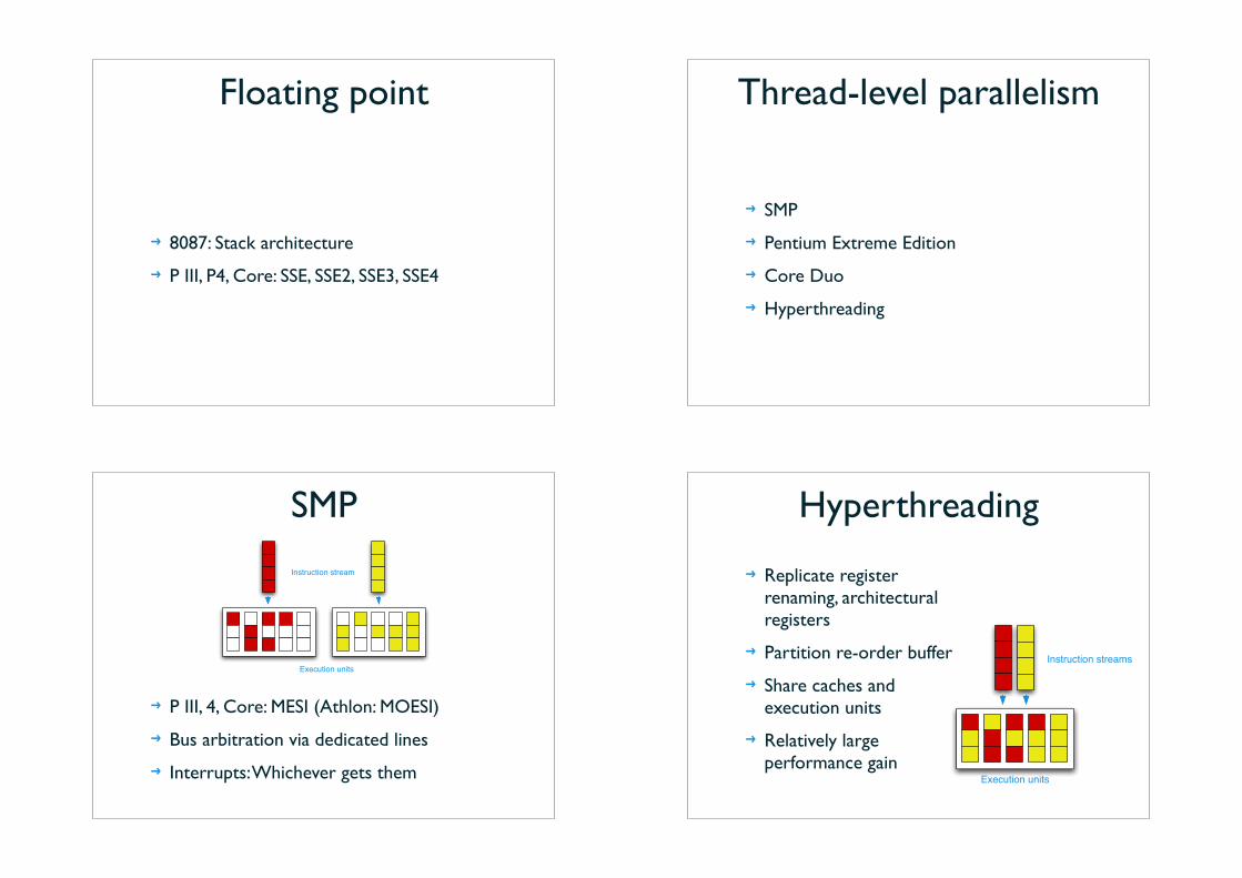
Floating point
! 8087: Stack architecture
! P III, P4, Core: SSE, SSE2, SSE3, SSE4
Thread-level parallelism
! SMP
! Pentium Extreme Edition
! Core Duo
! Hyperthreading
SMP
! P III, 4, Core: MESI (Athlon: MOESI)
! Bus arbitration via dedicated lines
! Interrupts: Whichever gets them
Instruction stream
Execution units
Image: arstechnica.com
Hyperthreading
! Replicate register renaming, architectural registers
! Partition re-order buffer
! Share caches and execution units
! Relatively large performance gain
Instruction streams
Execution units
Image: arstechnica.com
Page 9
Performance
! “Speed demon” P4 was disappointing
! Focus on ILP / TLP
! Dual-core designs
! Hyperthreading120 ,
a, 100-
I 25 50 63 75 a7 io0 125 200 i
Relative area (percentage)
Figure 2. Performance versus die area for different
decoder designs.
The load port would operate about 30 percent of the time
and the store port at about 10 percent of the time. This
proved to be the case, with less than a 1 percent performance
loss for this change.
Changing from a 4-2-2-2 decode template (four instruc-
tions per clock) to a 4-2-2 template (three instructions per
clock) also was a no-brainer, with no detectable performance
change on 95 percent of programs examined.
We also changed the renaming and retirement ports from
fourxmicro-ops per clock to three, which resulted in a slight-
ly larger, but still manageable 2 percent performance loss.
Finally, we reduced the L 1 cache size from 16 to 8 Kbytes.
In doing this, we took advantage of the full-frequency ded-
icated bus we had already chosen. Since the L1 cache is back-
stopped by a full bandwidth, three-clock L2 cache, the extra
L 1 misses that result from cutting the L1 cache size cause a
relatively minor 1.5 percent performance loss.
The reduction from four- to three-way superscalar opera-
tion and the reduction in L 1 cache size had some negative
impact on chest-thumping bragging rights, but we could not
justify the extra capacity by the delivered performance.
Further, tenaciously holding on to extra logic would have
resulted in significant negative consequences in die area,
clock speed, and project schedule.
As the design progressed, we eventually found that even
the first round of trimming was not enough. We had to make
further reductions to keep die size in a comfortable range,
and, as it turned out later, maintain clock frequency. This
required making further cuts, which resulted in detectable
performance loss, rather than the truly negligible losses from
the earlier changes.
We made two major changes. We cut back the decoder to
a 4-1-1 template from a 4-2-2 template. This amounted to
about a 3 percent performance loss. We also cut back the
branch target buffer from 1,024 to 512 entries, which barely
affected SPECint92 results (1 percent) but did hurt transac-
tion processing (5 percent). It was emotionally difficult (at the
time) for the microarchitecture team to accept the resulting
performance losses, but these results turned out to be criti-
cal to keeping the die area reasonable and obtaining a high
clock frequency. This kind of careful tuning and flexibility in
product goals was essential to the ultimate success of the
program.
It is important to consider the actual shape of the area-
performance curve. Most high-end CPU designs operate well past the knee of this curve. Efficiency is not a particularly
critical goal. For example, the market demands as much per-
formance as possible from a given technology, even when
that means using a great deal of silicon area for relatively
modest incremental gains
Figure 2 illustrates this effect. This graph charts the per-
formance of various instruction decoder schemes coupled
to a fixed execution core. All of the architectures discussed
earlier are clearly well past the knee of the performance
curve. Moving from point A (a 4-2-2-2 template) to point B
(4-2-2) is clearly the right choice, since the performance
curve is almost flat. Moving down to point C (4-1-1) shows
a detectable performance loss, but it is hardly disastrous in
the grand scheme of things. Point D (4-2-one we actually
considered at one time) occupies an awkward valley in this
curve, barely improved over point E (4-1) for significantly
more area and noticeably lower performance than point C.
As we converted the microarchitecture to transistors and
then to layout, execution quality became critical. All mem-
bers of the project team participated in holding the line on
clock frequency and area. Some acted as firefighters, han-
dling the hundreds of minor emergencies that arose.
This phase is very critical in any major project. If a project
takes shortcuts and slips clock frequency or validation to
achieve earlier silicon, the design often contains bugs and
suffers unrecoverable performance losses. This design phase
determines a project’s ultimate success. The best planned
and most elegant microarchitechire will fail if the design team
does not execute implementations well. As CPU architects,
we were very fortunate to work with a strong design and
layout team that could realize our shared vision in the result-
ing silicon.
THE PENTIUM P R O PROCESSOR ran DOS, Windows,
and Unix within one week of receiving first silicon. We had
most major operating systems running within one month.
We made a series of small metal fixes to correct minor bugs
and speed paths. The A2 material, manufactured using a 0.6-
micron process, ran at 133 MHz with a production-quality
test program, including 85 degree case temperature and 5
percent voltage margins).
The BO steppingincorporated several microcode bug and
speed path fixes for problems discovered on the A-step sil-
icon, and added frequency ratios to the front-side bus. Our
success with early Pentium Pro processor silicon, plus pos-
itive early data on the 0.35-micron process, encouraged us
to retune the L2 access pipeline. Retuning allowed for ded-
icated bus frequencies in excess of 200 MHz. We added one
clock to the L2 pipeline, splitting the extra time between
address delivery and path while retaining the full-core clock
frequency and the pipelined/nonblocking data access capa-
bility. The 0.6-micron BO silicon became a lSO-MHz, pro-
duction-worthy part and met our goals for performance and
frequency using 0.6-micron Pentium processor technology.
We optically shrank the design to the newly available 0.35-
14 IEEEMicro
Source: IEEE Micro
The future of IA-32
! EMT64
! Virtualisable
! Multicore
seuQnoit!!?s