B ERLINER T OR 3 . D-20099 H AMBURG hochschule für angewandte wissenschaften hamburg FACHBEREICH ELEKTROTECHNIK UND INFORMATIK university of applied sciences Degree course : Information Engineering Performed at Robert Bosch GmbH Stuttgart Supervisor at Bosch: Mr. Dipl.-Ing. J. Schimpke Supervising examiner: Prof. Dr.-Ing. B. Schwarz Second examiner: Prof. Dr.-Ing. F. Schubert Delivery day 14 th May 2002 Bachelor Thesis Hardware Tests and Software Development for Components of an Identification and Data Storage System applied in Assembly Lines Bin Fu
Transcript
BERLINER TOR 3 . D-20099 HAMBURG
hochschule für angewandte wissenschaften hamburg F A C H B E R E I C H E L E K T R O T E C H N I K U N D I N F O R M A T I K
university of applied sciences
Degree course : Information Engineering Performed at Robert Bosch GmbH Stuttgart Supervisor at Bosch: Mr. Dipl.-Ing. J. Schimpke Supervising examiner: Prof. Dr.-Ing. B. Schwarz Second examiner: Prof. Dr.-Ing. F. Schubert Delivery day 14th May 2002
Bachelor Thesis
Hardware Tests and Software Development for Components of an Identification and Data Storage
System applied in Assembly Lines
Bin Fu
- I -Preface
1 If it is not indicated in addition, all the components referred in this thesis is concerning of system ID40
Preface A controllable transport system should have an intelligent control ability so that it needs functionalities of read/write, recording and dealing with the current information, a central bus control or a decentralized control with internal processor. There is a team in Department BRL/EMT4 at Robert Bosch GmbH who has developped such kind of controllable transport systems since 15 years ago, which is so called Identification and Data storage system(ID). Nowadays the main product is ID80/E and is still being reformed continually, and the new design is ‘ID40’ that has a read-write-station(SLS) fixed on the assembly system and a mobile data tag(MDT) on the workpiece carrier by using the magnetic induction to communicate with each other, both sides could be programmed, and the SLS side could be controlled by a central host computer with a serial data path or by a decentralized control. At the beginning of this 13 weeks’ internship(July 15, 2001 – Octo 15, 2001), my task focuses on the new design ID401, which is being developed since 3 years. At first I examined the circuit of MDT ID40, afterwards I developped a C-Code of a read-write function for the micro controller of MDT ID40. During the internship, I leaned how hardware and software are combined in such a system, how software driver controls hardware performance, how to make a proper theoretical evaluation before real testing, etc. This thesis mainly describes system ID40, and focuses on some hardware tests and software development of component MDT ID40, moreover, a hardware test for Read-Write-Head (SLK) will be descripted as well. All tests include assignment descriptions, detailed process and results analysis. Herewith I am very grateful for Mr. Dipl.-Ing. J. Schimpke’s technical guidance and Mr. Dipl.-Ing. B. Waser’s supervision, as well as all my colleagues’ supports during the internship. Moreover, I thank Mr. Prof. Dr. B. Schwarz for his careful examination and kindly guidance to this thesis. My sincere thanks to all. Bin Fu
List of figures .................................................................................................................IV
Introduction and objectives........................................................................................... V
Introduction of identification and data storage system ID40................................................................V An ‘FMS’ – Flexible Assembly System for spark plug ...................................................................V Working principle of ID40 ............................................................................................................. VI Objectives of thesis............................................................................................................................. VI Topical highlights .............................................................................................................................. VII
1 Overview of an identification and data storage system - ID40 ............................ 1
1.1 Main components of ID40 ............................................................................................................1 1.2 Intermedium of data transmission.................................................................................................2 1.3 Data processing using ID40 ..........................................................................................................3
2 Introduction of MDT ID40 ...................................................................................... 4
2.1 Overview of MDT ID40 ...............................................................................................................4 2.2 Energy transmission system ........................................................................................................5 2.3 Transmission and receiving module ............................................................................................6 2.4 Signal demodulating and CPLD ...................................................................................................7 2.4.1 Protocol for recovery of the signal .......................................................................................7 2.4.2 Description of CPLD - XCR3064XL ...................................................................................8 2.5 Micro controller ............................................................................................................................8 2.6 External Memory ..........................................................................................................................9 2.6.1 Description of external memory chip - FM24160 .................................................................9
2.6.2 Command structure of external memory chip .....................................................................10
3 Hardware tests for MDT ID40 and Read Write Head (SLK)............................ 11
3.1 Tests of CPLD for MDT ID40 ....................................................................................................11 3.1.1 Functionality of CPLD (XCR3064XL) in MDT..................................................................12 3.1.2 Test of CPLD (XCR3064XL) for MDT ID40 .....................................................................13 3.1.3 Test of CPLD (XCR3032XL) for MDT ID40 .....................................................................16 3.2 Test of changing communication frequency for SLK.................................................................17 3.2.1 Theoretical analysis for the test ...........................................................................................19
3.2.2 Measurement results and conclusion ...................................................................................20
4 Software development with C for driver of MDT ID40 ..................................... 22
4.1 Fundmentals of communication between SLS/SLK and MDT ..................................................22 4.1.1 Specification of HF-Protocol ...............................................................................................23 4.1.2 Communication sequence ....................................................................................................23 4.2 Driver for MDT controller ..........................................................................................................26 4.2.1 Read-write function specification ........................................................................................27 4.2.2 Function requirements and process analysis...........................................................................27
List of figures Figure 1: An ‚FMS‘ -- Flexible Assembly System ................................................................V Figure 2: shows SLS and MDT using the Bosch FMS as an example............................... 2 Figure 3: A rough description of energy and data transmission by means of an RF field ................................................................................................................................................. 2 Figure 4: An example of central processing of MDT data .................................................. 3 Figure 5: Block diagram of MDT ID40 circuit...................................................................... 4 Figure 6: Two channels‘ rectifier for energy transmission of MDT ID40........................... 5 Figure 7: DC voltage on C2 of MDT when MDT is stationary in front of SLS ................... 6 Figure 8: Block diagram of transmission and receiving circuits of MDT ID40 ................. 6 Figure 9: Input Rx signal (above) and output Rx signal (down) of CPLD ......................... 7 Figure 10: Inputs and outputs of CPLD - XCR3064XL (44 pin) .......................................... 8 Figure 11: Inputs and outputs of PIC controller.................................................................. 8 Figure 12: Pin layout and functions of memory chip - FM25160 ....................................... 9 Figure 13: Table Op-code Commands of memory chip - FM25160 ................................. 10 Figure 14: Timing diagram of memory write (above) and memory read (below) of chip - FM25160................................................................................................................................ 10 Figure 15: Overview of testing for CPLD ........................................................................... 11 Figure 16: Pin’s configuration of CPLD ............................................................................. 12 Figure 17: Timing diagram of transmission signal Tx and receiving signal Rx before changing CPLD pin configuration measured by a 4-channel-oscilloscope ................... 13 Figure 18: Pin layout of CPLD (XCR3064XL) ..................................................................... 13 Figure 19: Changing pin configuration in .UCF file(DEC_OUT is changed to PIN23) .... 14 Figure 20: Timing diagram of Tx and Rx after changing CPLD pin configuration ......... 14 Figure 21: Timing diagram of original Rx, decoded Rx and Tx ...................................... 15 Figure 22: Total device resource summary of CPLD XCR3064XL.................................. 16 Figure 23: Rx decoding comparison of CPLD XCR3032XL and CPLD XCR3064XL....... 17 Figure 24: Signal receiving circuit of the SLK................................................................... 18 Figure 25: Timing diagram of the comparator PC74HCT132T input and output with communication frequency 1.25 MHz on the MDT ............................................................. 18 Figure 26: Timeing diagram with communication freqency 2.304 MHz on the MDT(Result 1)....................................................................................................................... 20 Figure 27: Timing diagram with communication frequency 2.304 MHz on the MDT(Result 2)....................................................................................................................... 21 Figure 28: State transition of communication sequence between SLS/SLK and MDT.. 22 Figure 29: Logon phase of communication between SLS and MDT ............................... 23 Figure 30: Data read and write of communication between SLS and MDT..................... 24 Figure 31: Main loop of the driver of MDT ID40................................................................. 26 Figure 32: Communication sequence between SLS/SLK and MDT................................. 27 Figure 33: Decision chart of Read/Write function for 2K memory of MDT...................... 28 Figure 34: Main differences between external memory chip FM25160(2K) and FM25640(8K)......................................................................................................................... 32 Figure 35: Timing diagrams of memory write (above) and memory read (below) for 8K ............................................................................................................................................... 32 Figure 36: Decision chart of Read/Write function for 2K memory of MDT...................... 33 Figure 37: Send “Read” Co-opcode................................................................................... 35 Figure 38: Send requested address ................................................................................... 36 Figure 39: Read out the data from the memory ................................................................ 36
- V –Introduction and objectives
Introduction and objectives
Introduction of identification and data storage system ID40 The Bosch identification and data storage system is specially developed for the automation and control of transport assembly system. Nowaday there are two main products ID80 and ID40. Bosch ID80 identification and data storage system is the old design and the main product in the moment, and ID40 introduced in this thesis is the new design, which is concentrated to develop by Department BRL/EMT4 of Bosch. The main differences between both systems are on the design of the Mobile Data Tag (MDT), which is the main component of the system. MDT ID40 is about 2/3 smaller than MDT ID80, because more micro chips e.g. CPLD XCR3064XL are implemented in the new MDT ID40 instead of many electric circuit in the old design ID80. Anyway, MDT ID40 has the same functionality and same working principles as MDT ID80, and many functionality blocks between both designs are totally same. The differences between both kinds of MDTs are only the layout of the electrical circuit and the using of some electronical elements.
An ‘FMS’ – Flexible Assembly System for spark plug Flexible assembly system has been widely used in industry since massive industrial production were prevalent all over the world. Products on the mobile workpiece carrier can be carried to specific working station by a flexible assembly system(FMS). A typical flexible assembly system for spark plug is shown in Figure 1, there are 5 working stations in this assembly line, including a robot arm at working station 5. It can be assumed that the spark plug
Figure 1: An ‚FMS‘ -- Flexible Assembly System [13]
intersection
- VI –Introduction and objectives
after processing by the robot arm would be processed by the human hand work, either be inspected at station 1, or be assembled at station 2, or anything else. Different stations might have different tasks, so for an intelligent transport system, it should know where the products should go according to its current state before the spark plug reaches each intersection. In other words, a control system on an FMS which can store the current information of the spark plug e.g. ‘waster’, can know the position of each mobile carrier, can choose the route for each mobile, can deal with the requests of the user and can process information indenpendantly is needed. With this control system, an ‘FMS’ can be a really intellegent transport system. The Bosch Identificaiton and Data Storage System ID40 is this kind of control system.
Working principle of ID40 As the destination of this control system, ID40 must have following characteristics:
• Be able to keep the products/system information in the memory • Be able to read and write the information • Ability to control a transport assembly system, e.g. direction of mobile carrier • A central control ability, which can process the current/stored information • Ability to communicate among each component • etc.
As to be introduced in following Chapter 1 and Chapter 2, the system works base on the wireless communication between its two components i.e. Mobile Data Tag(MDT) and Write Read Station(SLS). The MDT is mounted on the mobile workpiece carrier, so it will flow with the carrier. The MDT could store the information of workpiece on the same carrier or information of system. The SLS is mounted stationary on the assembly system, and as long as the MDT enters its inductive magnetic area, it will communicate with the MDT to read the information or write information from/into the memory of the MDT. According the result of the communication, the SLS will tell the system, where the workpiece carrier should go to, or tell the system, which state should be set, etc. In Chapter 1, these chacteristics will be instroduced in detail, and in Chapter 2, a particular introduction of MDT ID40 also will be given.
Objectives of thesis This thesis describes a series of hardware tests for the CPLD of the MDT and for the Write Read Head (SLK) respectively. CPLD acts as the decoder of the MDT, it remodulates the signal received from the SLS/SLK into the form which the processor can recognise. The SLK is something similar to the SLS, but it is not such a programmable device for the customer as the SLS, all the function has been defined by Bosch before it is sold out. But in the aspect of communicating with the MDT, it performs same characteristic as the SLS. The assignment description of these hardware tests are enumerated following:
• There are disturbances occuring on on the receiving signal Rx decoded by the CPLD sometimes while pulse appears on the transmission signal Tx in the same time, which is sent to the processor. The pin layout of the CPLD and the influence of the original receiving signal are assumed as the reason of the disturbancs and need be proved.
• The CPLD XCR3064XL is implemented in the MDT ID40, in order to save the original cost, a possibility to use a cheaper CPLD XCR3032XL to replace the original one need be proved.
- VII –Introduction and objectives
• 1.25MHz is the communication frequency between the MDT and the SLS/SLK, a possibility to change another communication freuqency need be proved.
This thesis describes also the development of a ‘Read/Write function’ for the driver software of the MDT controller. This driver is implemented in C, and acts as the soul of the MDT, which should be able to recognize the commands from the SLS/SLK and give the corresponding response. The implementation of this driver should obey not only the communication protocol between the MDT and the SLS/SLK, but also the specification of the memory chip. Therefore, the objectives of this thesis is to let the reader know the fundamental aspects of ID40, and it begins with an overall instroduction of the system and the MDT, then the hardware tests and software development described upper will be emphasized to instroduce. These aspects of the Identification and Data Storage System ID40 are enumerated following:
• Industrial application of ID40 • Main components of ID40 • Rationale of the wireless communication between two componets i.e. MDT and SLS/SLK of
system ID40 • Communication principle/protocol between two componets i.e. MDT and SLS/SLK of ID40 • Main data processing sorts of ID40 • Working principle of MDT ID40, including introduction of each functional block of MDT
ID40 • A driver software written in C for the processor of main component MDT ID40
Topical highlights The Bosch identification and data storage system ID40 is being developed mainly in two specific areas i.e. hardware and software. In the area of hardware development for ID40, measurements of working performance, tests of each compont and corresponding results analysis are indispensable, in order to make each component of ID40 work more steadily and precisely. In the area of software development for ID40, both overall driver software design and detailed coding must obey the specfic communication protocol and the specification of each component i.e. Complex Programmable Logic Device(CPLD), micro controller and external memory. This thesis contains four chapters and one summary at last, the first two chapters emphasize to introduce composition, main sorts and main components i.e. MDT and SLS of ID40. From Chapter 3, main topics turn to the detailed tasks for both hardware tests and software development. Description of these four chapters are enumerated following:
• Chapter 1: Overview of an identification and data storage system - ID40 An overview on identification and data storage system ID40 is to be described, main components and sorts, as well as principle of inductive data transmission will be introduced.
• Chapter 2: Introduction of MDT ID40 The emphasis will be turn to analyse one component of ID40 i.e. MDT ID40, most of electrical circuit block of MDT ID40 will be introduced, i.e. energy transmission circuit, transmission-receiving module, micro controller and external memory.
- VIII –Introduction and objectives
• Chapter 3: Hardware tests for MDT ID40 and Read Write Head (SLK) Guide the reader to more specific and detail things. A series of hardware tests to make the MDT work steadier are to be descripted, moreover, a test of SLK will also be described. All the records will be analysed in detail.
• Chapter 4: Software development with C for driver of MDT ID40 A C-Coding read/write function will be emphasized to introduce, in order to let the reader get a gerneral impression on the driver software development of ID40.
• Summary: This chapter expounds the differences between old design ID80 and new design ID40 presented in this thesis, and summarizes the results of all the hardware tests and software development mentioned in this thesis, as well as introduces the background and the destination of some tasks.
• Appendix: Bibliography, abbreviation reference and Source code of Read/Write function for
Micro controller of MDT ID40. ‘Bibliography’ enumerates all literatures or document which are used by the author, in this thesis all square brackets with number e.g. [8] means that the corresponding contents or figures are cited from indexed literature or document in the bibliography list. Appendix A - ‘Abbreviation reference’ enumerates all the abbreviations appeared in the thesis and their full names. Appendix B presents source code of Read/Write function for micro controller of MDT ID40.
- 1 –Overview of an identification and data storage system - ID40
1 Overview of an identification and data storage system - ID40
During the frontal introduction, the reader should have already known the usage of identification and data storage system ID40 and its rough working principle. And in this chapter, an introduction of main components and data processing modes of ID40, as well as the intermedium of data processing is to be given. After this chapter, the reader can get an overview of a complete ID40 system.
1.1 Main components of ID40 ID40 has mainly two components: Mobile Data Tag (MDT) and Read Write Station (SLS). The MDT is mounted on the mobile workpiece carrier, because of the function of keeping and processing the data, it is called ‘Mobile Data Tag’. The high memory capacity of the MDT permits the decentralized storage of such data as for instance: • Identity numbers • Workpiece data • Machine data • Set-up parameters • Test specifications • Production status data • Production parameters • Destination lists • etc The MDT allows for an unlimited number of data input or retrieval operations. The input of data into the MDT, and the retrieval of data from it, takes place through the stationary SLS. The SLS is equipped with: • Program memory • Data memory • Process inputs and outputs • Serial communication interfaces • Parallel data interfaces As shown Figure 2 there is a mobile workpiece carrier, which is fixed on the transport system, an MDT is stationed on the workpiece carrier, which can store the data of workpiece or data of system, as long as the MDT enters into the magnetic field of SLS, it will communicate and accomplish data exchange with SLS, as the full name of SLS – Read Write Station, the SLS can either read data from the MDT or write data to the MDT during the communication.
- 2 –Overview of an identification and data storage system - ID40
Figure 2: shows SLS and MDT using the Bosch FMS as an example[13]
1.2 Intermedium of data transmission Transmission of energy and data between MDT and SLS takes place inductively by means of a radio frequency (RF) field. Figure 3: A rough description of energy and data transmission by means of an RF field[13]
Figure 3 shows that when MDT is inside the RF field transmitted by the SLS, data transmission takes place between the MDT and the SLS. Data exchange can be carried out with the MDT stationary or in motion. During the data transfer, the MDT is energized exclusively by the SLS. Once the MDT leaves the RF field, data is maintained in the memory of the MDT.
MDT
SLS
Workpiece carrier
MDT side SLS side
Magnetic radio frequency field
- 3 –Overview of an identification and data storage system - ID40
1.3 Data processing using ID40 The ID40 system permits local or centralized processing of the MDT data. For centralized data processing, the SLS could be connected to a host system, for instance a master computer through a serial interface, or through a parallel interface e.g. to a Programmable Logic Controller(PLC). In this case, the host computer determines the program sequence. For local data processing, there is no connection to a host computer. The data is processed by programs which are stored in the SLS itself. There are a number of programs stored in the SLS, and as soon as the MDT enters the RF field of the SLS, the program which is activated is executed. Both types of data processing can be mixed.
Figure 4: An example of central processing of MDT data[6]
A ‘centralized processing’ identification and data storage system is shown in Figure 4, the SLS is connected to a host computer by a serial interface, data porcessing is carried out centrally by the host computer.
MDT SLS
Serial interface
Host computer
- 4 –Introduction of MDT ID40
2 Introduction of MDT ID40 MDT ID40 can not only store the information of the products and the system, but also deal with the requests from the SLS and afterwards can give the SLS corresponding response. The demension of MDT ID40 is about 2/3 smaller than the old product MDT ID80/E, because of using more micro chips, i.e. CPLD (XCR3064XL) replaces many electrical circuits of the MDT ID80/E. In this chapter an overview of the working principle of the MDT ID40 will be described in chief, moreover, most important blocks’ functionalities will be analysed in the total MDT circuit as well.
2.1 Overview of MDT ID40 The circuit of the MDT ID40 can be divided into following parts:
• Spool transmission of energy and data • Supply voltage of micro controller during communication period
Figure 5: Block diagram of MDT ID40 circuit
Receiving Circuit
Transimision Circuit
Clock generator
Micro Controller with memroy (PIC16LD65)
CPLD (XCR3064XL)
External Memory
(FM25160)
Energy Transmission circuit
Original Rx
Decoded Rx
Tx
Tx
Clockout
Reset
Serial Peripheral Interface(SPI) Bus
SLS
Clockin
MDT Side SLS Side
Vcc
Vcc
Vcc
Vcc Vcc
Radio Frequency(RF) Field
- 5 –Introduction of MDT ID40
• Clocking generated circuit for processor • Micro controller with memory • External memory • Transmission circuit • Receiving circuit
The block diagram of MDT ID40 is shown in Figure 5. The received signal(Rx) from receiving circuit will be docoded by the CPLD, then be sent to micro controller to process. The transmission signal can be sent to CPLD from the mirco controller, then be sent to transmission circuit, by means of an RF field it will be recoganised by the SLS. The micro controll is able to read and write the processed information to the external memory by a Serial Peripheral Interface(SPI) bus. The supply voltage is offered by the energy transmission circuit, the energy is charged by the SLS when the MDT is in the RF field. Except for reset generator and clock generator, each block will be depicted in detail in following chapters.
2.2 Energy transmission system The data and energy transmission between the SLS and the MDT is done by a electrical magnetic altering field with the frequency of 1.25MHz. The MDT lies at the sending range of the SLS, and its electric coil couples with the transmission coil of the SLS. The maximum induced amplitude of voltage of the MDT is ca. 20V, which depends on the distance between the MDT and the SLS.
Figure 6: Two channels‘ rectifier for energy transmission of MDT ID40 In order to generate the steady signal from the changeable signal, a two-channel-rectifier is used (Figure 6). The both half waves of the signal charge C2, which is with large capacity. This capacitor
Vcc
SLS
RF Field
MDT Side
- 6 –Introduction of MDT ID40
supplies the energy for all the MDT circuit. In the same time the capacitor (C2, C3) polishes the pulsing output of this rectifier. The voltage on C2 – Vcc (ca.16V) is unsteady, which depends on the distance between the MDT and the SLS. The rising speed of DC voltage Uin also depends on the distance between the MDT and the SLS. The system demands, when the distance between the SLS and the MDT is more than 4mm and less than 14mm, the system should work properly. Figure 7 shows the DC voltage on C2 when MDT is stationary, SLS does not communicate always successively with the MDT, there is an interval about 40ms.
Figure 7: DC voltage on C2 of MDT when MDT is stationary in front of SLS
2.3 Transmission and receiving module This module is the interface to the SLS in MDT ID40 circuit, which can receive the signals from the SLS or can send the signals to the SLS, and couples with the resonant circuit of the SLS. This module is also connected to the energy transmission block, and acts as ‘Input’ and ‘Output’ ports in MDT ID40.
Figure 8: Block diagram of transmission and receiving circuits of MDT ID40 Electric coils are implemented at each side of transmission and receiving module facing to the SLS, by which transmitted signal (Tx) from the CPLD can be sent directly. For the received signal (Rx), it must
5
15
10
-5
-10
-15
50 t / ms 150 250 350
Vcc(V)
40 320
Receiving Circuit
Transimision
Circuit
SLS
RF Field Coil
Schmidt Trigger (7WZ38)
Tx
Original Rx
Original Rx
CPLD
(XCR3064XL)
Tx
Decoded Rx
Pin 3
Pin 44
Pin 10
Pin 2
- 7 –Introduction of MDT ID40
be rectified by a schmidt trigger (7WZ38) in order to transfer the original half wave to half rectangular wave, which CPLD can recognise (Figure 8).
2.4 Signal demodulating and CPLD The signals from the SLS through the receiving circuit of the MDT need be demodulated again by a decoder in order for micro controller to realize the correct biniary information. For this purpose a CPLD chip XCR3064XL is implemented in MDT ID40.
2.4.1 Protocol for recovery of the signal In order to recover the signal, a Schmitt-Trigger (7WZ38) is set between the signal receiving circuit and the CPLD (XCR3064XL). The received information is interpreted by the following protocol: • Two symmetric rectangular pulses, which will be interpreted as binary code “1”. Every binary code
corresponds two periods of the signal with communication frequency 1.25MHz. • Two unsymmetric rectangular pulses, which will be interpreted as binary code “0”. Every binary
code corresponds two periods of the signal with communication frequency 1.25MHz as well. Ten such kinds of double pulses represents one bit, then it will be decoded according to the specified protocol by the CPLD.(Figure 9) Because:
Transfer Rate = Communication Frequency / 20 = 1.25MHz / 20 = 62.5 Kbps The time range of each bit is 1 / 62.5 Kbps = 16 us
Figure 9: Input Rx signal (above) and output Rx signal (down) of CPLD
- 8 –Introduction of MDT ID40
2.4.2 Description of CPLD - XCR3064XL A decoder is needed, which can demodulate receiving signals into the format that micro controller can recognize. It should also be able to divide the frequency of the clock as the requirement of the micro controller. In addition, the transmision signal (Tx) is also connected to the CPLD, but there are actually no combinational logic implemented between input and output of the transmission signals, it is only conventional for a later improvement. According to practical requirements, this decoder should also be small demension, low consume and price.Therefore, the CPLD chip XCR3064XL is implemented as the decoder of the MDT during the trial phase. Figure 10 shows the inputs and outputs of the XCR3064XL.
Figure 10: Inputs and outputs of CPLD - XCR3064XL (44 pin) XCR3064XL is a 3.3V, 64-Macrocell CPLD. A total of four function blocks provide 1,600 usable gates. Pin-to-pin propagation delays are 6.0 ns with a maximum system frequency of 145 MHz. Xilinx offers a TotalCMOS CPLD, both in process technology and design technique. The specified function of the CPLD is designed with a software from Xilinx ‘WebPACK XPLA Programmer’, afterwards the design can be programmed on the chip.
2.5 Micro controller Processing signals is the prime task of the MDT, which should be able to storage the data, be able to access the data in the memory and so on. In order to get this destination, a micro controller PIC16LC65 is implemented to act as the ‘CPU’ of the MDT.
The PIC16LC65 device has 33 I/O pins and 192 bytes of RAM. In addition, several peripheral features are available including: three timer/counters, two Capture/Compare/PWM modules and two serial ports. The PIC16LC65 has special features to reduce external components, thus reducing cost, enhancing system reliability and reducing power consumption. [11] The micro controller PIC16LC65 can process the input signal from the CPLD or from the external memory, then send output signal to the CPLD or the external memory.(Figure 11) In MDT ID40, the PIC controller is programmed by C, then program is converted to hex file, at last it is uploaded to the chip by an interface from company IAR. After these procedures, the MDT becomes an intelligent system, all the functions can be defined by the user.
2.6 External Memory In order to backup the processed data, e.g. identity numbers, workpiece data, production status etc, an external memory chip FM25160 - 16K bits (2K Bytes) Ferroelectric Random Access Memory (FRAM) is implemented, which can be manipulated by the micro controller.
2.6.1 Description of external memory chip - FM24160 The FM25160 is a memory employing an advanced ferroelectric process. A ferroelectric random access memory (FRAM) is nonvolatile but operates in other respects as a RAM. It provides reliable data retention for 10 years while eliminating the complexities, overhead, and system level reliability problems caused by EEPROM and other nonvolatile. [7]
Figure 12: Pin layout and functions of memory chip - FM25160 [7] The FM25160 (Figure 12) is a serial FRAM memory, which has 8 pins. SO and SI are connected to an industrial standard Serial Peripheral Interface(SPI) bus. The other side of the SPI bus is connected to the micro controller, all the opcodes and data are sent and received through this SPI bus.
- 10 –Introduction of MDT ID40
2.6.2 Command structure of external memory chip There are six opcodes that can be issued by the bus master to FM25160. They are listed in Figure 13 below. These opcodes control the functions performed by the memory. They can be divided into three categories. First are commands that have no subsequent operations. They perform a single function such as to enable a write operation. Second are commands followed by one byte, either in or out. They operate on the status register. Last are commands for memory transactions followed by address and one or more bytes of data.
Name Description Op-code value WREN Set Write Enable Latch 00000110 WRDI Write Disable 00000100 RDSR Read Status 00000101 WRSR Write Status Register 00000001 READ Read Memory Data 00AAA011 WRITE Write Memory Data 00AAA010
Figure 13: Table Op-code Commands of memory chip - FM25160 Figure 14 shows the operation of “Memory Write” and “Memory Read”. After chip is selected (CS), according to the SCK (Serial Clock) the first 8 bits on SI (Serial Input) are command of Write / Read, following 8 bits are the address which the user wants to write in or read out. “AAA” in first 8 bits are the highest three bits of the address, that means the address range of the memory is 0x 00 00 to 0x 07 FF. The last 8 bits are the data, if the operation is read, it takes place on SO (Serial Output), if the operation is write, it takes place on SI (Serial Output). These commands come from the SLS or the SLK, which are interpreted by the micro controller of the MDT.
Figure 14: Timing diagram of memory write (above) and memory read (below) of chip - FM25160[7]
- 11 –Hardware tests for MDT ID40 and Read Write Head (SLK)
3 Hardware tests for MDT ID40 and Read Write Head (SLK) A full-grown product must be tested thousands of times so that its different working performances can be proved. Many flaws of the products can be also found during the tests, moreover, each technical parameter also should be got by tests and experiments in the laboratory. The SLK has the similar function to the SLS. It may be puzzled for the readers to know the differences between both devices. As mentioned in the introduction chapter, the SLS has more complete funtions than the SLK , and it has its own programmable system, the customers can program and define some control functions by themselves. And the SLK has not this kind of ability, whose function is defined by BOSCH, after sold, the customers can not modify it by themselves. In the other aspects e.g read/write information from/to the MDT, deal with the information etc, they have same effects. In this chapter, some tests associated with the working performance of CPLD in MDT ID40 will be described, a possibility to exchange current CPLD (XCR3064XL) with another model of CPLD (XCR3032XL) will be described as well, at last, a test of changing communication frequency for the SLK will be explained in detail.
3.1 Tests of CPLD for MDT ID40 XCR3064XL is a programmable CPLD, which can be designed for different functions and implemented by a software from Xilinx called ‘WebPACK XPLA Programmer’, after design, compile and debug, user can upload the design to the CPLD by “XPLA Device Programming”.
XILINX Project navigator
Program uploading
CPLD (XCR3064XL)
Rx(transmission circuit)
Tx (micro controller)
Pin 44 Rx (micro controller)Pin 10
Pin 2
Clockin ClockoutPin 37 Pin 11
Tx (transmission circuit)Pin 3
Port LPT2
Figure 15: Overview of testing for CPLD
- 12 –Hardware tests for MDT ID40 and Read Write Head (SLK)
This process is described in Figure 15. A product with good quality should not only be able to work well under any working environment, but also be able to work steadily as long as possible. The focus of the following tests will be on the working performance of CPLD.
3.1.1 Functionality of CPLD (XCR3064XL) in MDT In MDT ID40, the CPLD is designed as following: Pin44 and Pin10 are designed as the receiving part (Rx), Pin44 receives the periodic rectangular signals, which are through the Schmitt-Trigger from the receiving circuit(Original Rx). After the CPLD’s demodulating these signals will be sent to the micro controller chip PIC16LD65, which acts as the CPU of a computer, it fetches and stores the data of memory with the uploaded program. A pin’s description of the CPLD can be found in Figure 10. The signals of original Rx (Pin44) and decoded Rx (Pin10) are described as Figure 9 in Chapter 2.4.1. Pin2 and Pin3 are designed as the transmission part (Tx), Pin2 is connected to the PIC Controller, which can get the transmitted signal, then through the CPLD, it is outputed at Pin3, which is connected to the transmission circuit, in the end the signal is sent to the SLS. There are no any combinational logic relations implemented between Tx Pin2 and Tx Pin3 in the CPLD, therefore they (input and output) are completely same. They could also connect directly without the CPLD, through a CPLD is just to offer a possibility to implement some functions later, so the name original Tx or decoded Tx will not be given as Rx, it is only one so called Tx in this thesis. The corresponding block diagram can be found in Figure 5 in Chapter 2.1, pin layout of the CPLD is described in Figure 10. Moreover, Pin11 offers the PIC controller the indispensable Clock, Pin27 offers the PIC controller RESET. An overall view can be found in following table Figure 16. It is an UCF file generated by ‘WebPACK XPLA Programmer’, which assigns the input and output ports for the CPLD. User can also change the pin layout of the CPLD by mean of modifying UCF file.
Figure 16: Pin’s configuration of CPLD
//UCF file created by Project Navigator NET "ASY_INP" LOC = ":PIN44"; NET "CPU_OSC" LOC = ":PIN11"; NET "DEC_OUT" LOC = ":PIN10"; NET "RESET" LOC = ":PIN27"; NET "CLOCK" LOC = ":PIN37"; NET "SEND" LOC = ":PIN35"; NET "TX_IN" LOC = ":PIN2"; NET "TX_OUT" LOC = ":PIN3"; #PINLOCK_END
- 13 –Hardware tests for MDT ID40 and Read Write Head (SLK)
3.1.2 Test of CPLD (XCR3064XL) for MDT ID40 Sometimes there are several disturbances taking place at decoded Rx (Pin10) of the CPLD of MDT ID40, while some pulses are coming from Tx Pin2 or Pin3(Figure 17). Pin10 is the decoded receiving signal (Rx), which should be sent to micro controller, Pin2 and Pin3 are the transmission signal (Tx), which are from micro controller and to transmission circuit respectively.(Figure 10) Although the disturbance doesn’t appear all the time, it could lead to fatal error for a complete communication.
Figure 17: Timing diagram of transmission signal Tx and receiving signal Rx before changing CPLD pin configuration measured by a 4-channel-oscilloscope In order to remove these disturbances away, it is important to find its reason. The reason were prefumed either both wires decoded Rx and Tx(Pin10 and Pin2) arranged too close, or the orginal receiving signal’s decoding error, or something else. 3.1.2.1 Change the CPLD pins’ layout The distance between Tx(Pin2) and Rx(Pin10) is too close, which is prefumed the reason why the disturbance happens, i.e. the signals on both pins disturb each other.
Therefore the first scheme is to reprogram the CPLD (XCR3064XL), and to move decoded Rx (Pin10) to another place, where is further from Tx Pin2 and Pin3(Figure 18).
Figure 18: Pin layout of CPLD (XCR3064XL)
CH1 2 V 200 uS CH2 2 V 200 CH1 2 V 200 uS CH2 2 V 200 uS
U (V) U (V)
t / uS t / uS 0 400 800 0 400
2 . 3 .
. 10
1200 800 1200 1600
Tx Tx
Rx Rx
disturbance impulse signal
- 14 –Hardware tests for MDT ID40 and Read Write Head (SLK)
Main procedure: 1. Take the CPLD (XCR3064XL) away from the MDT board. 2. Modify the .ucf file by Xilinx Project Navigator, and move Rx signal Pin10 to Pin23(Figure 19),
which is further away from Pin2 and Pin3(Figure 18) 3. Upload the modified file to the CPLD. 4. Solder the CPLD again on the original MDT board. 5. Disconnect decoded Rx (Pin10) from the board, then connect Pin23 to where pin10 connected to
originally on the board. 6. Recording by oscilloscope to observe if the unwanted impulses still appear at Pin23
Figure 19: Changing pin configuration in .UCF file(DEC_OUT is changed to PIN23)
Figure 20: Timing diagram of Tx and Rx after changing CPLD pin configuration
//UCF file created by Project Navigator NET "ASY_INP" LOC = ":PIN44"; NET "CPU_OSC" LOC = ":PIN11"; NET "DEC_OUT" LOC = ":PIN23"; NET "RESET" LOC = ":PIN27"; NET "CLOCK" LOC = ":PIN37"; NET "SEND" LOC = ":PIN35"; NET "TX_IN" LOC = ":PIN2"; NET "TX_OUT" LOC = ":PIN3"; #PINLOCK_END
CH1 2 V 100 uS, CH2 2 V 100 uS CH1 2 V 100 uS, CH2 2 V 100 uS
U (V) U (V)
t / us t / us 0 400 800 0 400 800 1200 1200
disturbance impulse signal
Tx
Rx Rx
Tx
- 15 –Hardware tests for MDT ID40 and Read Write Head (SLK)
Results are recorded in Figure 20, from the observation on them, it is easy to see that the disturbances are still at Pin23 when several pulses come at the transmitted signals Tx (Pin2 and Pin3), although decoded Rx(Pin23) are now the furthest Pin from Pin2 and Pin3 on the CPLD. It is obvious that the disturbance has no relation with the distance of each pins. 3.1.2.2 Test original receiving signal (RX) on CPLD This scheme is to measure the original signal from the receiving circuit orginal Rx (Pin44), the disturbed decoded signal Rx(Pin10) and the transmission signal Tx (Pin3) in the same time, then record the characteristics of these three signals, after the observation try to find if the disturbance has a relationship with the undecoded signal at the Pin44 of the CPLD. Figure 21 is the result of these three signals. The signal on the Channel 2 (original RX) has an obvious disturbance, it lasts about 1 uS. Because the scale of the measurement is quite small, i.e. 500 ns, the width of the disturbance looks a little large. It is shown in Figure 21 that the disturbance does not synchronise with the undecoded original Rx signal at the Pin44 of the CPLD, which means when this disturbance happens, the signal of original undemodulated Rx is not at rising or falling edge. It is also easy to find that the width of the double signals at the Pin44(original Rx), which takes place in the same time as the disturbance appears, have no specifical differences. As the demodulating regulation, which was introduced in Chapter 2.4.1, it is not difficult to conclude that the disturbance has no relationship with the original receiving signal at Pin44.
Figure 21: Timing diagram of original Rx, decoded Rx and Tx
CH1 2 V 500 ns, CH2 2 V 500 ns, CH3 2V 500 ns
U (V)
t / ns 1 uS
No abnormity
1000 2000 4000 3000
Tx
Original Rx
Decoded Rx
Disturbance impulse signal
- 16 –Hardware tests for MDT ID40 and Read Write Head (SLK)
3.1.3 Test of CPLD (XCR3032XL) for MDT ID40 In the modern industry, the original costs are always very important. If the products have good quality and low price in the same time, they will be more competitive. The CPLD chip XCR3064XL is used as decoder of the MDT, in order to save the original costs, a programmable chip XCR3032XL, which has similar functionalities to the CPLD chip XCR3064XL is recommended to replace it. Following table Figure 22 is copied from a *.FIT file, which can be generated automatically after the design is implemented by Xilinx Project Navigitor. It records detailed implementation information of the CPLD, e.g. device recource summary, total pin used, etc. -------------------------------------------------------------------------- | RESOURCE AVAIL. USED UTILIZATION |
Figure 22: Total device resource summary of CPLD XCR3064XL This table shows the total occupied device recource. As shown in Figure 22, one CPLD has 4 logic blocks, each block contains control terms(C-Terms), programmable logic array(PLA) product terms(P-Terms) or sum terms(S-Terms) and 16 macrocells. P-Terms and S-Terms are used to control the preset/reset and output enables of the 16 macrocells’ flip-flops. Each macrocell can be configured as either a D- or T-type flip-flop or a combinatorial logic function. The degree of occupied hardware can be seen, e.g. for I/O pins total 32 pins are available and 7 pins are used in this design, so the percentage of utilization is 7/32 = 21.88%. It’s not difficult to find that most of resources are only least occupied. The CPLD XCR3032XL is a 32 macrocell CPLD compared to a 64 macrocell CPLD – XCR3064XL. Except for the number of macrocells, both of them have nearly same property, e.g. same number of I/O Pins, same number of logic blocks, same requirement of supply voltage 3.3V etc. On the other hand, the price of XCR3032XL is about 2.- DM cheaper than that of XCR3064XL in Germany. The main task of the CPLD is to demodulate the Rx signal to the controller, to transfer the Tx signal (without any processing on it) and to offer the controller the processing clock. Therefore, before testing, XCR3032XL is assumed theoretically to be competent to the requirement of the MDT. Main procedure of the test: 1. Upload the same function file as the XCR3064XL to a new CPLD XCR3032XL by Xilinx Project
Navigator. 2. Take away the original CPLD (XCR3064XL) from the MDT board. 3. Solder the new CPLD (XCR3032XL) on the MDT board. 4. Measure the results by an oscilloscope.
- 17 –Hardware tests for MDT ID40 and Read Write Head (SLK)
Figure 23: Rx decoding comparison of CPLD XCR3032XL and CPLD XCR3064XL
The results are recorded by an oscilloscope as shown in Figure 23. The upper figure is from XCR3032XL, comparing both figures it is not difficult to find that they have the same characteristics as decoder part. As explained in the chapter “Recovery of the signal”, signal at the Pin44 original Rx comes from the receiving block, and after the decoding, the signal at the Pin10 decoded Rx will be sent to the controller, it must be the style that the controller can recognise. The period of the signal at the Pin44 is about 1.56us, every period of the signal has two double impulses. If both impulses in one period have the same characteristics, then ten periods will be decoded to “1”, otherwise they will be decoded to “0”. The CPLD XCR3032XL finishes the same task for receiving signal decoding as XCR3036XL in this test. For other aspects, i.e. clock decoding, reset generating etc, they also have same effects. Therefore, it would be a reasonable scheme to replace the CPLD XCR3064XL in the decoder part of the MDT.
3.2 Test of changing communication frequency for SLK In order for the Read Write Head (SLK) to adapt the different working environments, a series of tests for SLK are to be done. The destination of these tests is to find the new configuration of circuit after the communication frequency between the MDT and the SLK is changed in order to adapt the different
CH1 2 V 2 uS, CH2 2 V 2 uS
t / us
t / us
U / V
U / V
Double symmetric signal
Double unsymmetric signal Double symmetric signal
Double unsymmetric signal
16 12 8 4 24 20 28
16 12 8 4 24 20 28
32
32
Original Rx
Original Rx
Decoded Rx
Decoded Rx
CPLD XCR3032XL
CPLD XCR3064XL
- 18 –Hardware tests for MDT ID40 and Read Write Head (SLK)
countries’ frequency laws. The original communication frequency between the MDT and the SLK is 1.25 MHz, and during this test it will be changed to 2.304 MHz. Figure 24: Signal receiving circuit of the SLK Figure 24 is the block diagram of the signal receiving block of the SLK. The comparator PC74HCT132T in Figure 24, which can be used to recover the signals from the ‘transmission-receiving-circuit’. Rx input(Pin1) and reference voltage(Pin2) are the inputs of the comparator, and Pin3 is the Rx output, which shows the modulated signal and whose form should be same and synchronise as transmission signal Tx of the MDT. Detailed specification is in Figure 24. As the shown Figure 25 it is easy to see that Pin2 offer a reference voltage i.e 2V to compare with the received signal Rx at Pin1, if the amplitude of Rx input is more than the reference voltage 2V, the output Pin3 will be low (0V), otherwise it will be high (5.0V). So after the signal goes through this comparator, it will be recovered orderly.
Figure 25: Timing diagram of the comparator PC74HCT132T input and output with communication frequency 1.25 MHz on the MDT
CH1 2 V 100 uS, CH2 2 V 100 uS
2V
U (V)
t / us 200 800 600 400
Rx Input(Pin 1 of
comparator)
Rx Output(Pin 3 of
comparator)In this case, the SLK communicates with MDT ID80 Time range of each bit = 16 us
Transimision and Receiving
Circuit
RF Field Coil
Comparator
(PC74HCT132T)
Pin3
Pin2 Pin1
2V R9 C8
SLK side MDT side
R7
Rx Output
Reference voltage
Uin(t)
Uout(t)
C7
GND
Band-pass filter
Rx Input
- 19 –Hardware tests for MDT ID40 and Read Write Head (SLK)
Figure 25 shows the characterics of input and output of the comparator before changing the communication frequency.
3.2.1 Theoretical analysis for the test As the definition of this test, the communication frequency from the MDT is changed to 2.304 MHz, which means the width of every signal from the MDT will be only half of the original one. The transfer rate can be got from the communication frequency by the transmission factor n = 20
Original transmission rate: KbpsMS 5.622025.1
==
New transmission rate: KbpsMS 2.11520
304.2' ==
Therefore original and new time range of each bit will be:
Original time range: usK
t 165.621
== New time range: usK
t 68.82.115
1' ==
The signal through the receiving circuit of the SLK, then it needs to pass a ‘Band-pass filter’, which comprise two resistants R7, R9 and two capacitors C7,C8 (Figure 24). The original values of R7, R9 and C7, C8 are 8.2K, 51K and 300pF, 47pF respectively. As shown in Figure 24, the frequency response can be got:
Frequency repsonse: )(1
)()(8977979787
2
97
CRRCRCjRRCCRCj
UinUoutF
+++−==
ωωωωω
Insert the original value of each parameter, the equation will be:
Frequency response: ωω
ωωω
jj
UinUoutF
317.110854.310536.6)()( 295 +×−×
== −−
According to frequency response, amplitude response and phase response also can be got:
The maximum of amplitude is Amax = 1/1.317 ≈ 0.76 at ω = 13.02 Hz, A(ω) is a bell-shaped function revealing the bandpass characteristic. )(ωϕ is partly negative(low) and partly positive(highpass).At the maximum ω = 13.02 Hz there is zero phase shift.
The real situation of the circuit is much more complicated than theoretical evaluation. As already know, the new load time for each bit will be less than the original load time because of increasing communication frequency, therefore, proportion of R7/R9 is to be decreased in order to make more voltage drop at output. In order to see the influence of the capacitor, C8 will also be decreased to make the time constant τ8 smaller along with the reduction of time range of each bit. The other elements in this band-pass filter will keep unchanged.
- 20 –Hardware tests for MDT ID40 and Read Write Head (SLK)
Signal lost
3.2.2 Measurement results and conclusion In this test, the main task is to measure Rx input(Pin1) and Rx output(Pin3) of the comparator, and compare them with Tx(Pin2) of the CPLD(XCR3036XL) of the MDT ID40 in the same time. In principle, the wave form between Pin3 of comparator and Pin2 of the CPLD should be same. According to this requirement, the scheme of the test is formulated: 1. Select suitable capacitors C8(10, 22, 27, 33, 47pf) and resistant R7(1, 2, 5, 8 KΩ).
2. Solder them on the SLK board one by one, then measure Pin1 and Pin3 of the comparator by the
oscilloscope. 3. Try to find the best configuration result from all the tests.
Figure 26: Timeing diagram with communication freqency 2.304 MHz on the MDT(Result 1) Result 1 analysis:
The result in Figure 26 proves it not accordant to the requirement. The second impulse on the channel2(Transmission signal of the MDT) disappears on the channel1 (Receiving signal on the SLK). If you pay attention to the original receiving signal on the input of comparator (channel 3), you will find that the second impulse is evidently too little to reach the “reference voltage” i.e. 2V from the Pin2 of the compatator. In the same time, whichever capacitor C8 in the list is used, it doesn’t help for the second pulse to reach 2V. Therefore, C8 can be seen that it has no influence to improve the results. For Uout gets more voltage drop, R7 should be decreased or R9 should be increased.
CH1 5 V 50 uS, CH2 5 V 50 uS, CH3 5 V 50 uS
<2V
U (V)
t / us 100 200 400 300 Rx Input
(Pin 1 of Comparatorof SLK)
Rx Output(Pin 3 of Comparator
of SLK)
Tx (MDT ID40)
R7=8K2, C8=27p, R9=51K on the SLK
- 21 –Hardware tests for MDT ID40 and Read Write Head (SLK)
Figure 27: Timing diagram with communication frequency 2.304 MHz on the MDT(Result 2) Result 2 analysis:
This result(Figure 27) looks much better than last one. The readers should still pay attention to the second impulse at the channel3 (Pin1 of PC74HT132T), and compare it to the corresponding signal in Figure 26. From the comparator the “reference voltage” about 2V can be found. Here R7 is nearly 0, and from a series of tests it can be found, if R7=0, however large C8 is, the result like Figure 26 can be always found. Conclusion: From a series of tests it can be found that R9 of the SLK can stay at 51K, at the same time R7 is recommended to set to 0 (or move it away from the circuit), then keep the other same, then the SLK could adapt the new communication frequency 2.304 MHz. After this change, this circuit will not be a band-pass filter any more, but this can be ignored for the result of testing for changing communication frequency.
CH1 5 V 50 uS, CH2 5 V 50 uS, CH3 5 V 50 uS
>2V
U / V
t / us 100 200 400 300
Rx Input(Pin 1 of Comparator
of SLK)
Rx Output(Pin 3 of Comparator
of SLK)
Tx (MDT ID40)
R7=0K, C8=47p, R9=51K on the SLK
- 22 –Software development with C for a driver of MDT ID40
4 Software development with C for driver of MDT ID40 As developing each kind of system with internal processor, an intelligent driver software is indispensable. There is a micro controller PIC16LC65 implemented in the MDT, which can process all the information inputing and outputing. It is actually controlled by a driver which is developed specially for this controller. In this chapter, fundmentals of communication i.e. HF-Protocol will be introduced at first, then the driver of MDT micro controller will be shown, in which a read-write to memory function will be especially thrown emphasis on introducing so that an overview of the driver can be given.
4.1 Fundmentals of communication between SLS/SLK and MDT Here at first an introduction of communication fundamental between SLS/SLK and MDT will be given so that an idea to get to know how each system component communicates with each other will be depicted. The driver software for the MDT micro controller must obey this protocol anyway.
Figure 28: State transition of communication sequence between SLS/SLK and MDT Explaination of Figure 28 is depicted as following, each index in following text corresponds same index in Figure 28: 1) Power up sequence from the MDT is received, which means the MDT has already been in the
range of RF field of SLS/SLK, communication begins. 2) Acknowledge(ACK) on WAIT-instr is received, no instructions for the MDT in the wait list. All
information has been sent, go to ‘Send End’.
Disconnected
Send WAIT
Send END
Session o.k.
Drive Protocols
Session failed
1)
2)
3)
9)
4) 5) 6)
7) 8)
- 23 –Software development with C for a driver of MDT ID40
3) ACK on END-instr is received, the session finishes without error. 4) ACK on WAIT-instr is received, at least one instruction for the MDT in the wait list. 5) Run until instructions-queue working out 6) ACK or last instruction received, all information has been sent, go to ‘Send End’. 7) WAIT-cycle can not execute the protocol again successfully, session fails. 8) Communication is cancelled during the processing, session fails. 9) END-instr can not be proved, session fails.
4.1.1 Specification of HF-Protocol All the communications between MDT and SLS/SLK are agreeable to HF-Protocol, which will be also introduced following. The HF-Protocol is used by the communication of the MDT in the ID40 System. The communication takes place in the area between the SLS(SLK) and the MDT with high frequency, while both of them identify the first PowerUp-character.
4.1.2 Communication sequence The HF-Protocol is performed only when a communication partner – MDT is in the HF area. Then the MDT initialize a “Session” after a logon sequence is received. The state transition diagram of the communication sequence can be seen in Figure 28. Before the data exchanging takes place, the communication partner MDT must logon with the SLK/SLS. The phase of the “logon” has following task: • To identify a valid communication partner MDT • To detect the error status of the MDT
Figure 29: Logon phase of communication between SLS and MDT
PowerUp CheckSum Instruction
Wait CheckSum
ACK CheckSum instr received
Logon Terminated
Acknowledge
confirm
MDT Startup SLK
Session startup
- 24 –Software development with C for a driver of MDT ID40
Figure 29 shows the logon phase. When a confirmation of ‘PowerUp’ sent by MDT is realised by the SLK, the SLK tells the MDT ‘Wait’, after SLK receives acknowledge(ACK) from MDT again, logon phase is terminated. After the successful logon phase, the data exchanging according to the communciation protocol begins.
Figure 30: Data read and write of communication between SLS and MDT
In order to protect the data, even parity is used, and is appended to the end of the telegram inversely. For example, “1-Byte-Instruction” will be transferred by two bytes. The first byte is the opcode, the second byte is the inverse opcode (CheckSum). Some of transmission parameters are described following:
Data to store 1-Byte-Write-Instruction OpCode CheckSum
ACK CheckSum
SOD data CheckSum
1-Byte-Read-Instruction OpCode CheckSum
Instruction Instruction received
confirm Instruction
Instruction received
Data to store
- 25 –Software development with C for a driver of MDT ID40
Transmission rate = 62500bps 8 data bits 1 start bit 1 stop bit 1 bit even parity Figure 30 describes 3-Byte-Read/Write-Instruction and 1-Byte-Read/Write-Instruction. For 1-Byte-Read-Instruction, SLK sends read OpCode to MDT at first, then the instruction for transferring data starts with SOD (Start Of Data). The instruction for every time’s confirmation starts with ACK (Acknowledge). 4.1.3 Relationship between communication principle and MDT driver In Chapter 4.1.2 the main communication protocol was introduced. Implementing the driver of the MDT controller must obey this protocol. Following a part of source code of the driver will be introduced, in order to make a better understanding. This part of code will be activated after the SLS send a “read byte” command. You can compare the source code one line by one line with Figure 30 “3-Byte-Read-Instruction”. Because this driver is for the MDT, only the response of the MDT part will be discussed.
Case O3_REBYDI: if (TestAdr()) //if requested address out of range WriteTxBuffer(NAK); //send not acknowledge WriteTxBuffer(~NAK); //send CheckSum else ucCKS = 0; //Reset CheckSum SetTxHelp(); WriteTxBuffer(SOD); //send Start Of Data <execute.c>
1. Test the sent address, if it is illegal, send a “NAK” (Not Acknowledge) by the command “WriteTxBuffer()” to the SLK. Otherwise, it sends “SOD” to the SLK, which means the data will start to send. “SOD” is the first element of this response instruction.
Note: “NAK” can not be found in Figure 30 because only the main process is discussed, the “error case” was not discussed in this chapter.
FramDriver(1,ucByteCnt,ucAdrH,ucAdrL); //Get the data from the memory for(Lenght =0; Lenght<=ucByteCnt-1; Lenght++) WriteTxBuffer(Value[Lenght]) ; //Get the data from the receiver buffer
- 26 –Software development with C for a driver of MDT ID40
2. Get the data from the memory by function “FramDriver()”, and store them into a variable “Value”, then send the value to the SLK, which is the second element of this response instruction. In the same time “checksum” is refreshed continually.
3. Send the last element of the response instruction “checksum”. Every part concerning of the communication with the SLK is implemented according to the “HF-Protocol”, this “read byte” is only an example to make the readers understand it easily.
4.2 Driver for MDT controller Main process of the driver is described as Figure 31. A main loop waits for a request, as long as it receives a request, decoder will conclude a parameter “MDTStat”, if go on processing. If so, it uses the “executer” function, which is the “headquarters” part of the program to decide which action will be activated according to the request. The following read-write function is one of these actions, which need be activated by “executer” as the corresponding request.
Figure 31: Main loop of the driver of MDT ID40
Encode
WAIT
decode
Executer
request
MDTStat<>EXESTAT
MDTStat=EXESTAT
bTimeOut=1
- 27 –Software development with C for a driver of MDT ID40
Figure 32 describes the process of the communication, at first the request from the SLS/SLK side, it was sent to the MDT by RF field, then after the decoding of the MDT CPLD, the request is proceded by a micro controller, then controller deals with the write/read request to the memory through a SPI bus.
Figure 32: Communication sequence between SLS/SLK and MDT
4.2.1 Read-write function specification A read-write function need be implemented, which is described as following: After a specific request from the SLS/SLK is received by the MDT, read-write function should be activated. According to the request of the SLS, it can either write specific information into specific address of the MDT’s memory, or read specific information from the specific address of the MDT’s memory, after either of action, the MDT gives the SLS response. All these actions obey to the communication principle which was described in the last chapter.
4.2.2 Function requirements and process analysis According to the requirement, following parameters will be needed in the function: • Conclusion for read / write • Length of write / read • Start address with low bits and high bits • Data Figure 33 is the decision chart of read-write function for 2K external memory. It is explained following:
Profibus
RF field
SLS/SLK Receiver Decoder
Micro Controller External memory SPI Bus MDT side SLS/SLK side
Data path
Data path
- 28 –Software development with C for a driver of MDT ID40
1. After the function is activated, the first step is to conclude if the given address is out of the memory range(0x000 – 0x7FF) of the MDT, if not, the program goes on processing, otherwise it stops and return 0, session fails.
2. Here only the processing case is discussed. The function concludes if the action is to read or to
write. 3. If to read, send Chip Select(CS) enable signal to memory chip. 4. Send a read request to memory chip, in the same time send the high three bits of the address to the
memory chip. 5. Send the low eight bits address to the memory chip 6. Fetch the data output from the memory chip. 7. The executing time of the loop depends on how many data are needed. 8. The write operation in this function is similar to the read operation, the difference compared to the
read operation is to send memory write request. 9. After all operations are executed, set the CS unable. The decision chart Figure 33 is acctually one function of ‘executer’ Figure 31.
Figure 33: Decision chart of Read/Write function for 2K memory of MDT
If out of the address range (0x000 - 0x07FF)? Yes No
Return 0; If read?
Yes No Set memory chip CS=0(Enable); Send “read” request; Send address; Fetch value; Set memory chip CS=1(Unable); address++;
For (i=0; i<length; i++)
Set memory chip CS=0 (Enable); Set “write” enable; Send “write” request; Send address; Write value; Set memory chip CS=1 (Unable); address++;
For (i=0; i<length; i++)
Return 1;
- 29 –Software development with C for a driver of MDT ID40
4.2.3 Detailed implementation In detailed implementation two kinds of situations should be dealt with. One situation is the MDT with 2K memory chip(FM25160), the other is the MDT with 8K memory chip(FM25640) in order to process more information. Both implementations will be introduced in following chapters. 4.2.3.1 Implementation for 2K memory chip The function is defined as UCHAR FramDriver(UCHAR IfRead, UCHAR Length, UCHAR StartAddrH, UCHAR StartAddrL) in the head file memory.h. • IfRead is a to conclude if the action is read or write. • Length is the time which is requested. • StartAddr and StartAddl is the address of the first element, i.e. start address. • Type of return value UCHAR is defined as ‘unsigned char’. The complete program of this function will not be explained in this chapter. The whole source code of this function will be appended in the end of this report. Here the main procedure will be explained block by block. Read
#ifdef _FRAM SSPBUF = SPI_READ + (StartAddrH<<3); //send read request and high 3 bits address while (!BF); //wait for BF=1 #ifndef _DEBUG BF = 0; #endif
...........
SSPBUF = StartAddrL++; //Send the low eight bits address while (!BF); #ifndef _DEBUG BF = 0; #endif
<memory.c>
- 30 –Software development with C for a driver of MDT ID40
This block is for execution of reading. At first set memory chip enable, then send the read request and high 3 bits of the address to the memory chip by the SPI bus, at last send the low eight bits address to the memory chip. Here the definition of the variable SPI_READ in the head file define.h must be mentioned:
Please go it over in Figure 13. It is easy to find that all defined values are same as the corresponding Op-code commands of the external memory chip FM25160. SPI_READ means read command on SPI bus, SPI_WREN means read enable on SPI bus, and so on. In the program StartAddrH is shifted to left three bits. In the definition of FM25160 the command “READ” is defined as “00AAA011”, “AAA” means high three bits of the address, so the read request and high three bits address can be sent in the same time by one command. Moreover SSPBUF is defined as the SPI buffer.
if (StartAddrL==0x00) //If low address is up to FF StartAddrH++;
<memory.c>
This block gets the value by the SPI buffer and puts it to a global variable Value[i], this global variable can be used by every *.c program of the project. After all actions finish, the function will set CS to “1” to make it unable. The last two line’s code is to deal with the overflow of the low byte. Write
- 31 –Software development with C for a driver of MDT ID40
Write action is a little different from Read action. At first a Write Enable request SPI_WREN must be sent by the SPI buffer.
RAMCS = 0; //Chip enable __no_operation(); #ifdef _FRAM SSPBUF = SPI_WRITE+(StartAddrH<<3); //send write request and high 3 bits address while (!BF); //wait until BF=1 #ifndef _DEBUG BF = 0; #endif ......... SSPBUF = StartAddrL++; //send low byte while (!BF); #ifndef _DEBUG BF = 0; #endif <memory.c>
This block is similar compared to the “Read” part, which send write request and high three bits of the address, then send the low byte of the address. It is not difficult to understand it if comparing the corresponding part in “Read”.
SSPBUF = Value[i]; //Write the value while (!BF); #ifndef _DEBUG BF = 0; #endif __no_operation(); RAMCS = 1; //Chip enable if (StartAddrL==0x00) //If low byte out of range StartAddrH++; <memory.c>
This block is similar to “Read” part as well, write the value by SPI buffer, set chip enable after all the actions, and at last deal with the case of low byte’s overflow.
- 32 –Software development with C for a driver of MDT ID40
4.2.3.2 Implementation for 8K memory chip In real working environment a memory chip often needs to store more information, although the standard MDT is equipped with 2K memory chip (FM25160), a possibility to be equipped with more memory capability still need be tested. 8K Memory chip (FM25640) is picked out to experiment, and it has the different specifications from 2K memory chip (FM25160), the main difference is described following (Figure 34): 2K memory chip (FM25160) 8K memory chip (FM25640) Memory range 0x 00 00 – 0x 07 FF 0x 00 00 – 0x 1F FF Max SPI frequency Up to 2.1 MHz Up to 5 MHz Supported SPI mode Mode 0 (CPOL=0, CPHA=0) Mode 0 & 3 (CPOL, CPHA=0, 0 & 1, 1)
Figure 34: Main differences between external memory chip FM25160(2K) and FM25640(8K) Fortunately, the Pin configuration between FM25160 and FM25640 is completely same, so if a FM25640 replaces a FM25160 on the MDT board, nothing on hardware has to be changed.
Figure 35: Timing diagrams of memory write (above) and memory read (below) for 8K[8] Obviously, the most difference between two kinds of memory chips is the range of the memory. To compare the Figure 35 to Figure 14, it is obvious to find their different address inputing wises. Because of this, some source codes must be modified in the memory accessing function UCHAR FramDriver(UCHAR IfRead, UCHAR Length, UCHAR StartAddrH, UCHAR StartAddrL). Compare the decision chart Figure 36 and memory write/read specification to the corresponding one of 2K memory chip Figure 33, it is not difficult to find that the Read/Write function for 8K memory has one step more because the high 5 bits address can not be sent with the opcode as the Read/Write function for 2K memory.
- 33 –Software development with C for a driver of MDT ID40
Figure 36: Decision chart of Read/Write function for 2K memory of MDT Read
RAMCS = 0; //Chip enable __no_operation(); #ifdef _FRAM SSPBUF = SPI_READ; //Send read request while (!BF); //Wait until BF=1 #ifndef _DEBUG BF = 0; #endif ....... SSPBUF = StartAddrH; //Send high byte address while (!BF); #ifndef _DEBUG BF = 0; #endif SSPBUF = StartAddrL++; //Send low byte address while (!BF);
If out of address range (0x000 – 0x7FFF) Yes No
Return 0; If read?
Yes No Set memory chip CS=0(Enable); Send “read” request; Send high bits address; Send low bits address; Fetch value; Set memory chip CS=1(Unable); address++;
For (i=0; i<length; i++)
Set memory chip CS=0 (Enable); Set write enable; Send “write” request; Send high bits address; Send low bits address; Write value; Set memory chip CS=1 (Unable); address++;
For (i=0; i<length; i++)
Return 1;
- 34 –Software development with C for a driver of MDT ID40
#ifndef _DEBUG BF = 0; #endif <memory.c>
According to the specification of “memory read” in Figure 35, the high byte is not sent together with “Read” request such as 2K memory chip, but is sent respectively one byte by one byte. Apart from this block, the other is same as that of 2K memory chip, therefore it is not to be elaborated again. Write
According to the specification of 8K “memory write” in Figure 34, the high byte and low byte address are sent respectively.
4.2.4 Result analysis In this chapter, a measurement by a 4-channel oscilloscope will be depicted. It records the state of the SPI bus after the MDT receives a “read byte” command from SLS side, because the micro controller deal with all information concerning of the memory chip by the SPI bus. Several commands are sent by a software “COMSLS.EXE” at the SLS side:
- 35 –Software development with C for a driver of MDT ID40
ff 20 03 10 01 ff 25; //send data to SLS buffer 3c 01 23; //send data from the SLS buffer to MDT memory 2c 03 01 23; //read from the MDT memory
The syntax of these instructions will not be explained detailedly, what important is just the mean of these instructions, the first instruction means four bytes data “0x10, 0x01, 0xFF, 0x25” are sent to the SLS buffer, the second instruction means the SLS sends all data in its buffer to the MDT memory address 0x1023, the third instruction means to read out the data from the MDT memory address 0x0123. Following some measurements will be done, the detailed methods is to measure the SPI bus between the MDT controller and the memory by a 4-channel oscilloscope, as the “read byte” function for 8K memory is activated. Note: From Figure 37 to Figure 39, configuration of the channels is
Channel1 Channel2 Channel3 Channel4 SI SO CS SCK
1. Observe Figure 37, this is the beginning part of the memory accessing, SI sends 0x03 to the memroy
chip, which tells the memory chip – “read” action will begin. In the source code, it is implemented by “SSPBUF = SPI_READ;” Tip: compare the “read” regulation of Figure 35.
Figure 37: Send “Read” Co-opcode 2. In Figure 38, the process of sending the requested address can be observed, the left part sends the
high byte of the address 0x01, the right part sends the low byte of the address 0x23. In the source code it is implemented by “SSPBUF = StartAddrH;” and “SSPBUF = StartAddrL++;” A delay after every action is set in detailed implementation, so the measurements of every action are not successive.
CH1 500 mV 1uS, CH2 5 V 1uS, CH3 5 V 1uS, CH4 5V 1uS
U
t / us 4 2 6 10 8
SI
CS
SCK
SO
- 36 –Software development with C for a driver of MDT ID40
Figure 38: Send requested address 3. In Figure 39, the process of data ouput on the SO (Channel2) can be seen, A, B, C and D are 0x10,
0x01, 0xFF and 0x25 respectively. In the source code you can also find the corresponding part
D (B)
D (D)
Figure 39: Read out the data from the memory
…
U
CH1 500 mV 1uS, CH2 5 V 1uS, CH3 5 V 1uS, CH4 5V 1uS
CH1 500 mV 1uS, CH2 5 V 1uS, CH3 5 V 1uS, CH4 5V 1uS …
…
U
0x10 0x01
CH1 500 mV 1uS, CH2 5 V 1uS, CH3 5 V 1uS, CH4 5V 1uS
…
U
0xFF 0x25
t / us 4 2 6 8 4 2 6 8
t / us 4 2 6 8 4 2 6 8
t / us 4 2 6 8 4 2 6 8
SI
CS
SCK
SO
SI
CS
SCK
SO
SI
CS
SCK
SO
- 37 –Software development with C for a driver of MDT ID40
4. All these results will be stored in the variable “VALUE” temporarily, afterward they will be sent to
the buffer of the SLS. From the analysis it is easy to see how important a driver is, it actually controlls the communication procedure and task, but it must also obey the protocol of the hardware. This driver is still being improved by Bosch developping group.
- 38 –Summary
Summary MDT ID80 has been developed since 15 years, each component has been namely tested for thousands of times, therefore, each of them has quite a steady and precise working performance. MDT ID40 is the new design, many working performances still need be tested and proved. Its circuit is made up of several functional blocks, mainly they are energy transmission block, transmission-receiving block, PIC controller, external memory, CPLD. As the demodulator part of the MDT, the CPLD chip is tested primarily. In order not only to work more properly and more steadily, but also to decrease the original costs. So in Chapter 3 describes following fullfilled tests for MDT ID40: 1. Tests of CPLD XCR3064XL for reasoning of an unexpected disturbance impulse. There is an
unexpected disturbance impulse signal occurring on decoded receiving signal(Pin 10) of the CPLD. Pins’ layout arranged too close and the original receiving signal influencing processed receiving signal are presumed as the reasoning of the disturbance signals. After testing, both presumptions were pulled down, which can be got rid of the possiblity as disturbance happening.
2. Test of CPLD XCR3032XL for a possiblity to replace CPLD XCR3064XL in MDT ID40 circuit.
The CPLD chip XCR3032XL is about 1 EURO cheaper than the CPLD chip XCR3064XL. As the current design on the CPLD is not so large, after a theoretical analysis on the requirement of the design, XCR3032XL is assumed that it can replace original XCR3064XL. After testing, it is proved that XCR3032XL performs same characteristics as original XCR3064XL. So it would be reasonable to replace XCR3064XL by XCR3032XL.
Moveover, the new products ID40’s communication frequency can not be used in the different countries all the same, because the different communication frequency laws among them. 1.25MHz, which is used in ID40 as the communication frequency, is commercially forbidden in some countries. Therefore a possibility to use different communication frequencies need be proved. In the MDT side it is easy to change the communication frequency by modifying the program of the CPLD and the controller without changing any hardware configuration, however, in the SLK or the SLS side, some configurations of the circuits must be modified so that it can “read” the information with the different frequency from the MDT. With 2.304 MHz communication frequency, the SLK was tested in order to find the corresponding best configuration of a low pass in the circuit. Because the complexity of a real huge electrical circuit, it is always difficult to find the exact solution by calculating theoretically. Therefore, such a scheme was excuted that at first some probable results were evaluated, then modify a capacitor and a resistance round these theoretical results in the SLK circuit was tried to approach the final solution. Finally, several possibile new configurations for this low pass in the SLK signal receiving circuit were found, each of them performs properly under the new communication frequency. In the last chapter, a Read/Write function for the MDT controller was introduced, then an overview of the driver software for MDT ID40 was given. The Read/Write function must obey not only an HF-protocol specially for communication but also the functional definition of the external memory, which was described at the beginning of Chapter 4. This function supports the controller have the ability to access the external memory, write and fetch the data of the memory, which makes the MDT be able to either store or get the information of the products or the system. In Chapter 4, the detailed driver written in C implementation and corresponding results of this Read/Write function for both 2K and 8K external memory was explained respectively. In summary, the main components i.e. SLS/SLK and MDT of the Bosch Identification and Data Storage System ID40 have the abilities to communicate with each other by means of a RF field, and still be able to exchange, store and deal with the information. Recur to these characteristics, a transport
- 39 –Summary
system e.g. FMS, equiped with ID40 can really be a controllable and intelligent transport system, which can widely be applied in the varied industrial fields.
- 40 –Bibliography
Bibliography [1] Donald G. Fink, H. Wayne Beaty
ISBN 0-07-020975-8 McGraw-Hill Book Company, 1987
Standard Handbook for Electrical Engineers
[2] Paul R. Gray, Robert G. Meyer ISBN 0-471-87493-0 Copyright 1977, 1984, by John Wiley & Sons, Inc
Analysis and Design of Analog Integrated Circuits (Second Edition)
[3] Michael Rose ISBN 3-7785-2574-3
Mikroprozessor PIC16CXX
[4] Anne.Koenig/Manfred.Koenig ISBN 3-7723-4284-1
Das PICmicro Profi-Buch
[5] Brian W. Kernighan/Dennis M. Ritchie ISBN 0-13-110370-9 Copyright 1988, 1978 by Bell Telephone Laboratories, Incorporated.
The C Programming Language
[6] Andreas Böhm Robert Bosch GmbH
Entwicklung eines busfähigen Transponder Schreib-/Lesesystem
[7] Ramtron International Corporation http://www.ramtron.com/products/standalone.asp
Data sheet of ‘FM25160 16Kb FRAM Serial Memroy’
[8] Ramtron International Corporation http://www.ramtron.com/products/standalone.asp
[11] Microchip Technology Inc. http://www.microchip.com/11110/helper.htm
Data sheet of ‘PIC 16C63A/65B/73B/74B – 8 Bit CMOS Microcontrollers with A/D Converter’
[12] Robert Bosch GmbH Spezifikation HF-Protokoll Version 2.0
- 41 –Appendix A
Abreviation references ACK Acknowledge CPLD Complex Programmable Logic Device CS Chip Select FMS Flexible assembly system FRAM Ferroelectric Random Access Memory HF High Frequency MDT Mobile Data Ttag NAK Not Acknowledge PB SLS program file PLA Programmable Logic Array PLC Programmable Logic Controller RF Radio Frequency RFID Radio Frequency Identification System SLK Read-write-head SLS Read-write-station SOD Start Of Data SPI Serial Peripheral Interface
- 42 –Appendix B
Source code of Read/Write function for Micro controller of MDT ID40 <Memory.c> /*Read/Write function for 2K bytes external memory chip:*/ UCHAR FramDriver(UCHAR IfRead, UCHAR Length, UCHAR StartAddrH, UCHAR StartAddrL) UCHAR i; if((StartAddrH>0x07)||((StartAddrH==0x07)&&((0xFF-StartAddrL)<=Length))) return 0; //if the given memory address is out of range of 0x000 - 0x7FF else if (IfRead==1) //if read for(i=0;i<Length;i++) RAMCS = 0; __no_operation(); #ifdef _FRAM //High byte of address SSPBUF = SPI_READ + (StartAddrH<<3); //read while (!BF); #ifndef _DEBUG BF = 0; #endif #else SSPBUF = SPI_READ; //read while (!BF); #ifndef _DEBUG BF = 0; #endif SSPBUF = R_SYS_H; //address output while (!BF); #ifndef _DEBUG BF = 0; #endif #endif SSPBUF = StartAddrL++; while (!BF); #ifndef _DEBUG BF = 0; #endif
SSPBUF = StartAddrL; while (!BF); #ifndef _DEBUG BF = 0; #endif SSPBUF = Value[i]; //data is written while (!BF); #ifndef _DEBUG BF = 0; #endif __no_operation(); RAMCS = 1; #ifndef _DEBUG #ifndef _FRAM WriteWait(); #endif #endif StartAddrL++; if (StartAddrL==0x00) StartAddrH++; return 1; <Memory.c> /*Read/Write function for 8K bytes external memory chip*/
UCHAR FramDriver(UCHAR IfRead, UCHAR Length, UCHAR StartAddrH, UCHAR StartAddrL) UCHAR i; if((StartAddrH>0x1F)||((StartAddrH==0x1F)&&((0xFF-StartAddrL)<=Length))) return 0; //if the given address is out of range of 0x000-0x7FF else if (IfRead==1) //if read for(i=0;i<Length;i++) RAMCS = 0;
- 45 –Appendix B
__no_operation(); #ifdef _FRAM //High byte of address SSPBUF = SPI_READ; //read while (!BF); #ifndef _DEBUG BF = 0; #endif #else SSPBUF = SPI_READ; //read while (!BF); #ifndef _DEBUG BF = 0; #endif SSPBUF = R_SYS_H; //adresse output while (!BF); #ifndef _DEBUG BF = 0; #endif #endif SSPBUF = StartAddrH; //High byte of address while (!BF); #ifndef _DEBUG BF = 0; #endif SSPBUF = StartAddrL++; //low byte of address while (!BF); #ifndef _DEBUG BF = 0; #endif SSPBUF = SPI_READ; //data read in while (!BF); #ifndef _DEBUG BF = 0; #endif Value[i] = SSPBUF; __no_operation(); RAMCS = 1; if (StartAddrL==0x00) StartAddrH++; else //if write for(i=0;i<Length;i++)
- 46 –Appendix B
RAMCS = 0; __no_operation(); SSPBUF = SPI_WREN; //Write Enable 0x06 while (!BF); #ifndef _DEBUG BF = 0; #endif __no_operation(); RAMCS = 1; __no_operation(); RAMCS = 0; __no_operation(); #ifdef _FRAM SSPBUF = SPI_WRITE; //write while (!BF); #ifndef _DEBUG BF = 0; #endif #else SSPBUF = SPI_WRITE; //write 0x02 while (!BF); #ifndef _DEBUG BF = 0; #endif SSPBUF = StartAddrH; while (!BF); #ifndef _DEBUG BF = 0; #endif #endif SSPBUF = StartAddrH; //High byte of adresse output while (!BF); #ifndef _DEBUG BF = 0; #endif SSPBUF = StartAddrL++; //Low byte of adresse output while (!BF); #ifndef _DEBUG BF = 0; #endif SSPBUF = Value[i]; //the written data output while (!BF); #ifndef _DEBUG
- 47 –Appendix B
BF = 0; #endif __no_operation(); RAMCS = 1; #ifndef _DEBUG #ifndef _FRAM WriteWait(); #endif #endif if (StartAddrL==0x00) //if low byte address StartAddrH++; return 1; <excute.c> /*The function, which can conclude and determine what the micro controller should do according to the specific request from the SLS side, it can activate the Read/Write function of <memory.c> */ case O3_REBYDI: //Read Byte Direct if (TestAdr()) //if address is not available WriteTxBuffer(NAK); //send ‘not acknowledge’ to the SLS WriteTxBuffer(~NAK); else ucCKS = 0; SetTxHelp(); WriteTxBuffer(SOD); //send ‘start of data’ to the SLS FramDriver(1,ucByteCnt,ucAdrH,ucAdrL);//call read/write function, first parameter 1 means ‘read’
for(Lenght =0; Lenght<=ucByteCnt-1; Lenght++)
WriteTxBuffer(Value[Lenght]) ; //send the read data to buffer ucCKS ^=Value[Lenght]; //Checksum refresh ucCKS ^= SOD; WriteTxBuffer(~ucCKS); ucCKS = 0;
- 48 –Appendix B
break;
case O3_WRBYDI: //Write Byte Direct if (ucDecStat == D_OPC) if (TestAdr()) //if the given address is not available WriteTxBuffer(NAK); //send ‘not acknowledge’ to the SLS WriteTxBuffer(~NAK); else ucDecStat = D_SOD; WriteTxBuffer(ACK); //send ‘acknowledge’ to the SLS WriteTxBuffer(~ACK); bDoPrefetch=1; else ucDecStat = D_OPC; Lenght =0; while (Lenght <= ucByteCnt)
Value[Lenght] = ReadRxHelp(); //Get the written data
Lenght++; ; FramDriver(0,ucByteCnt,ucAdrH,ucAdrL); //call the read/write function, the first parameter 0 means ‘write’ WriteTxBuffer(ACK); WriteTxBuffer(~ACK); break;
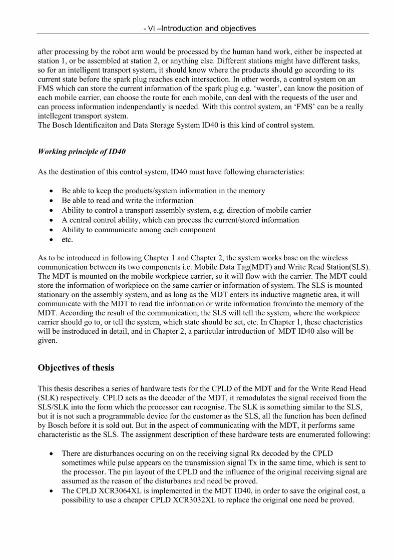
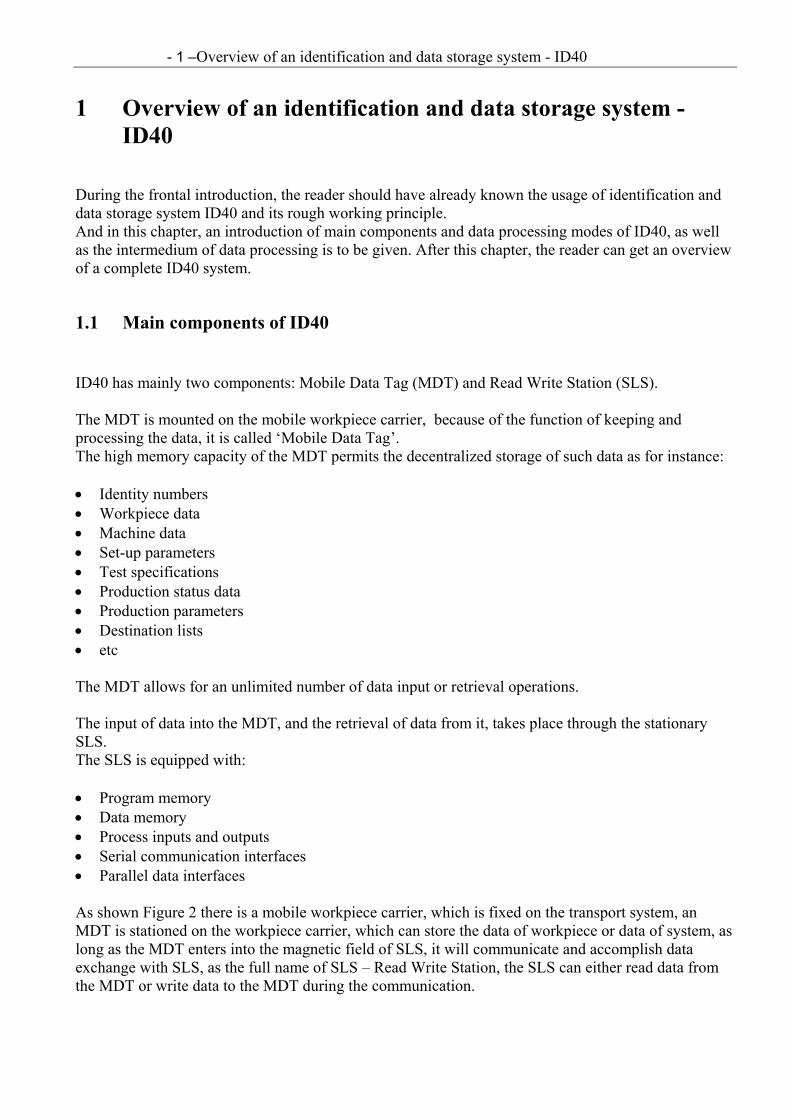
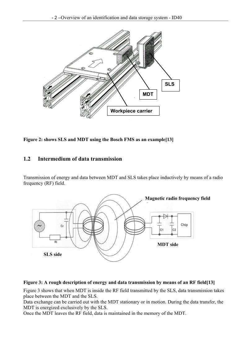
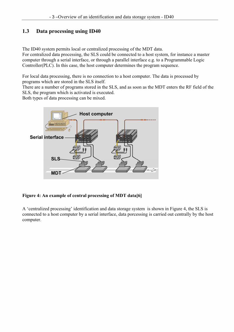
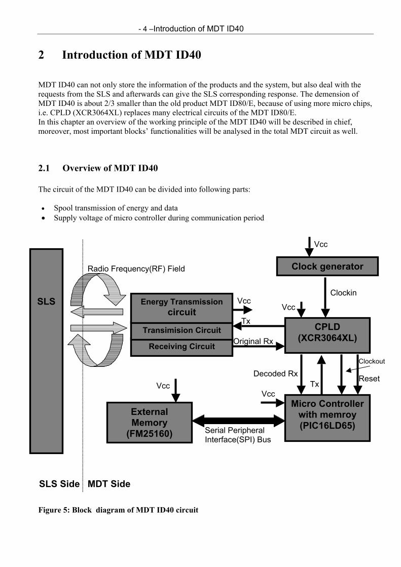
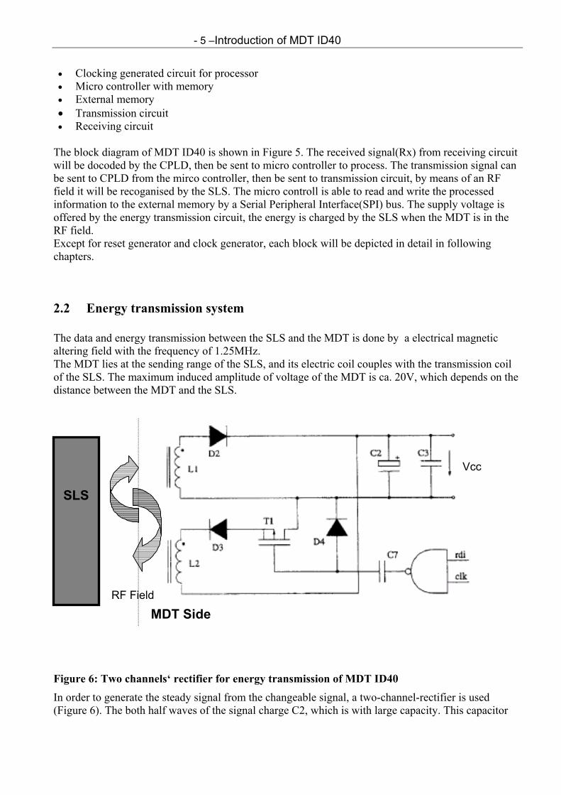
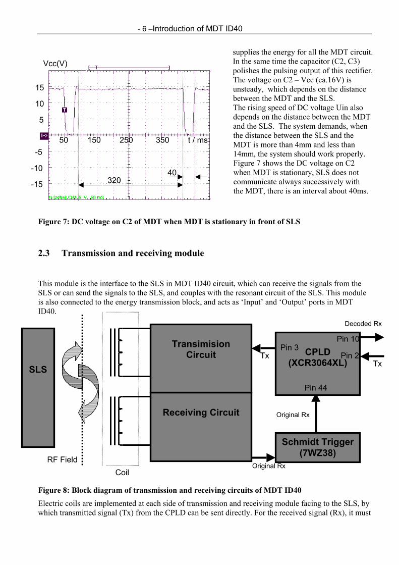
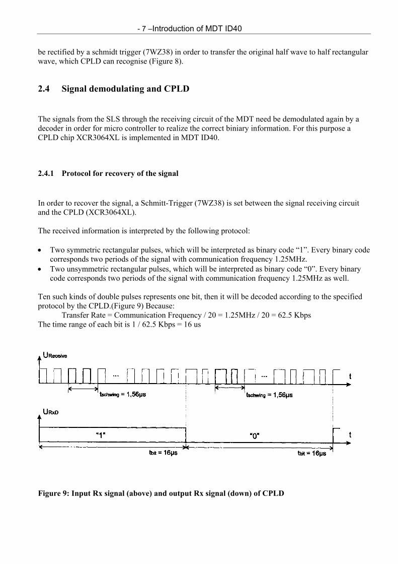
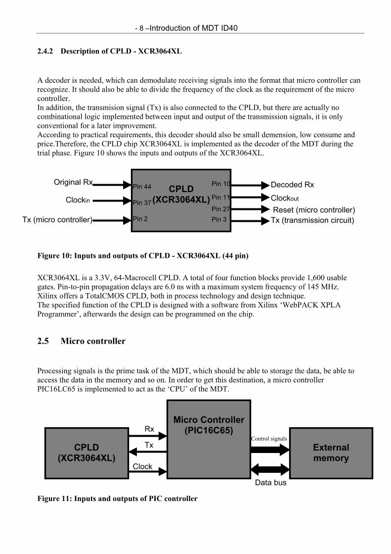
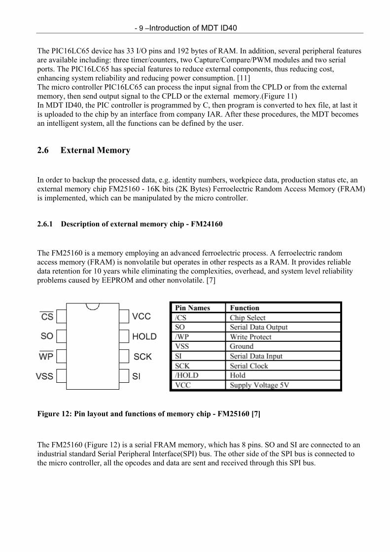


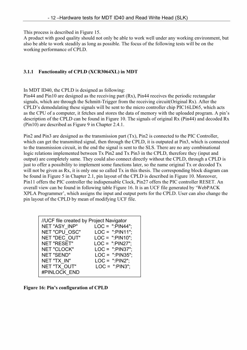
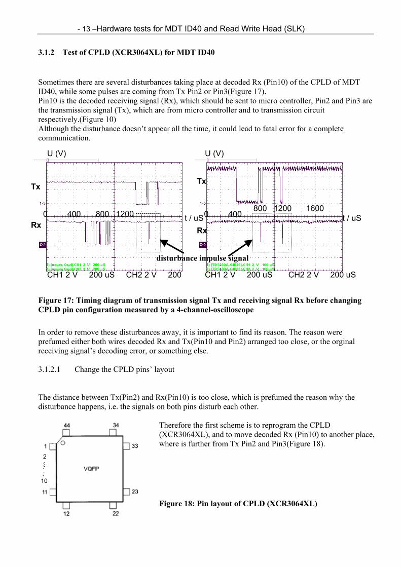
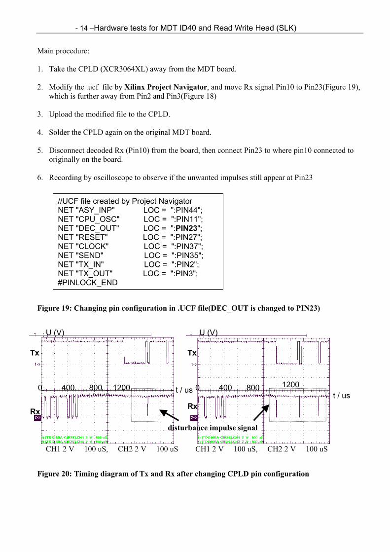
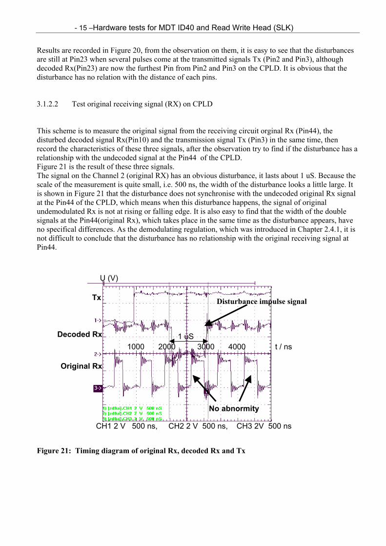
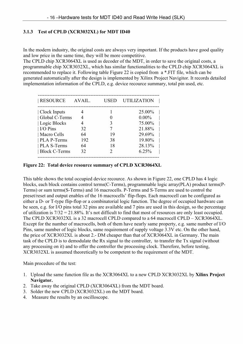
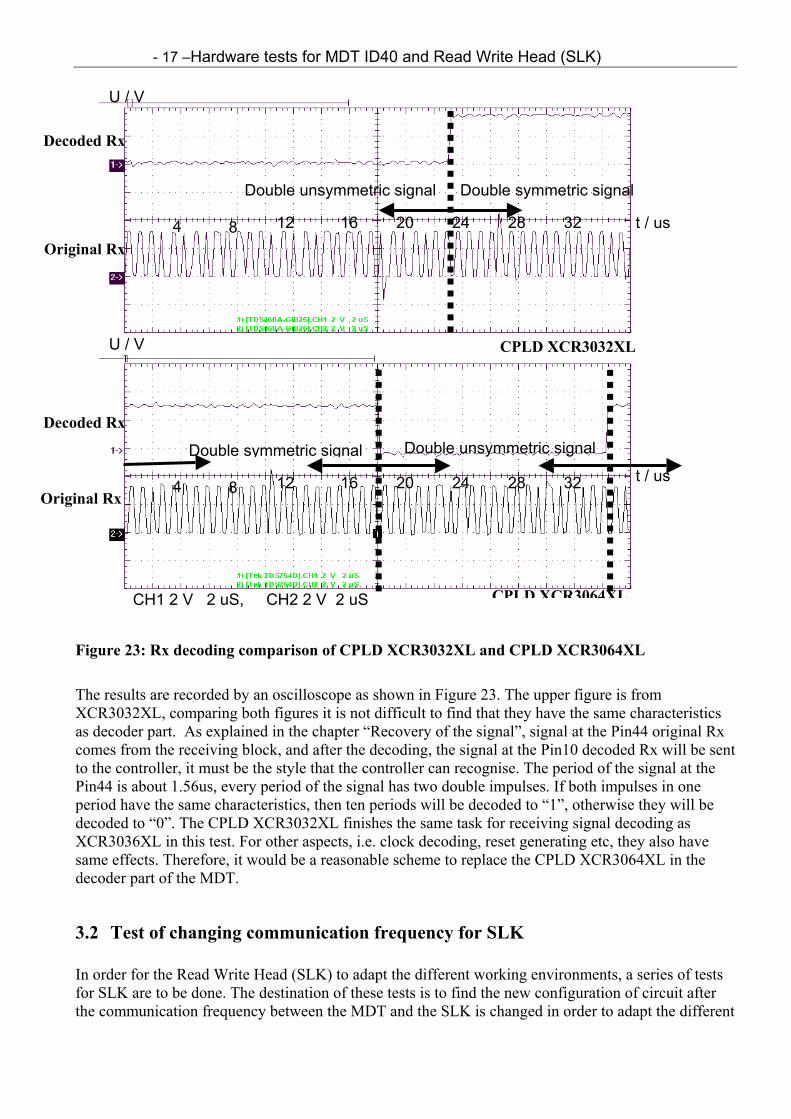
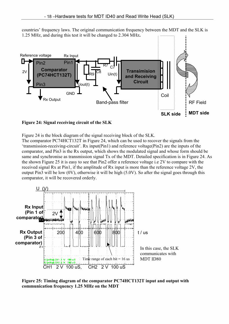

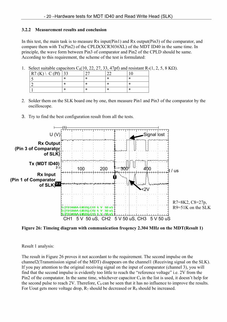
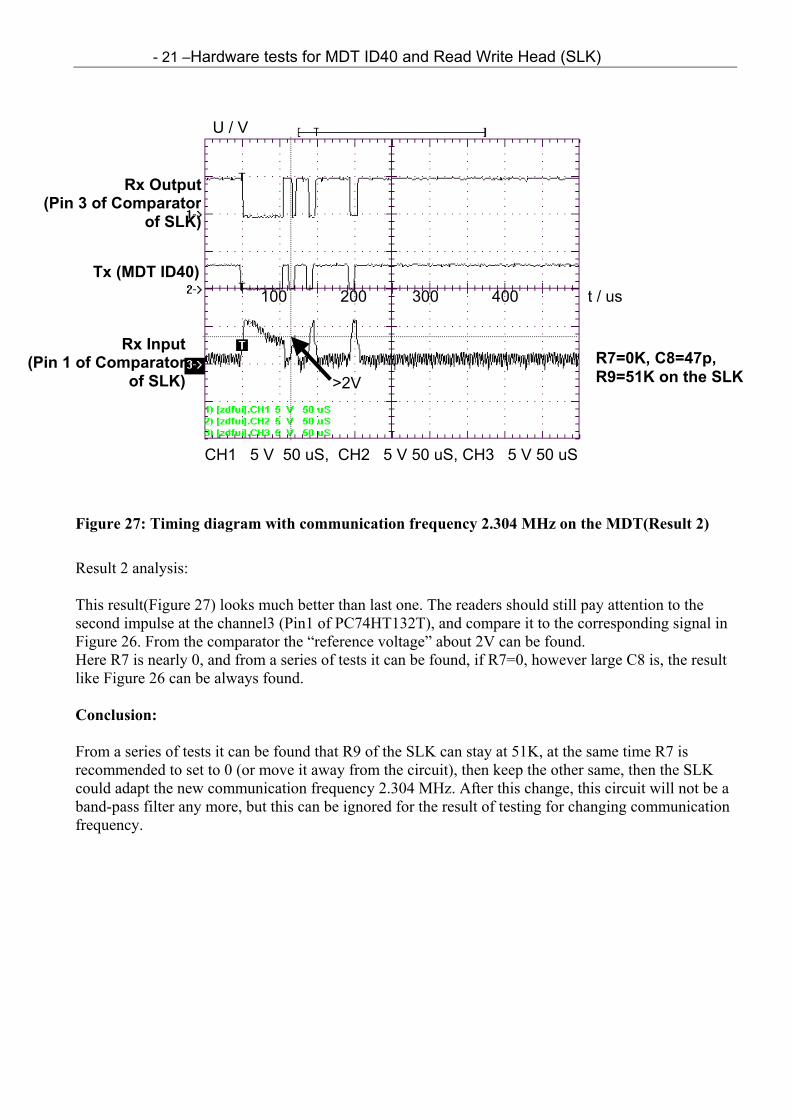
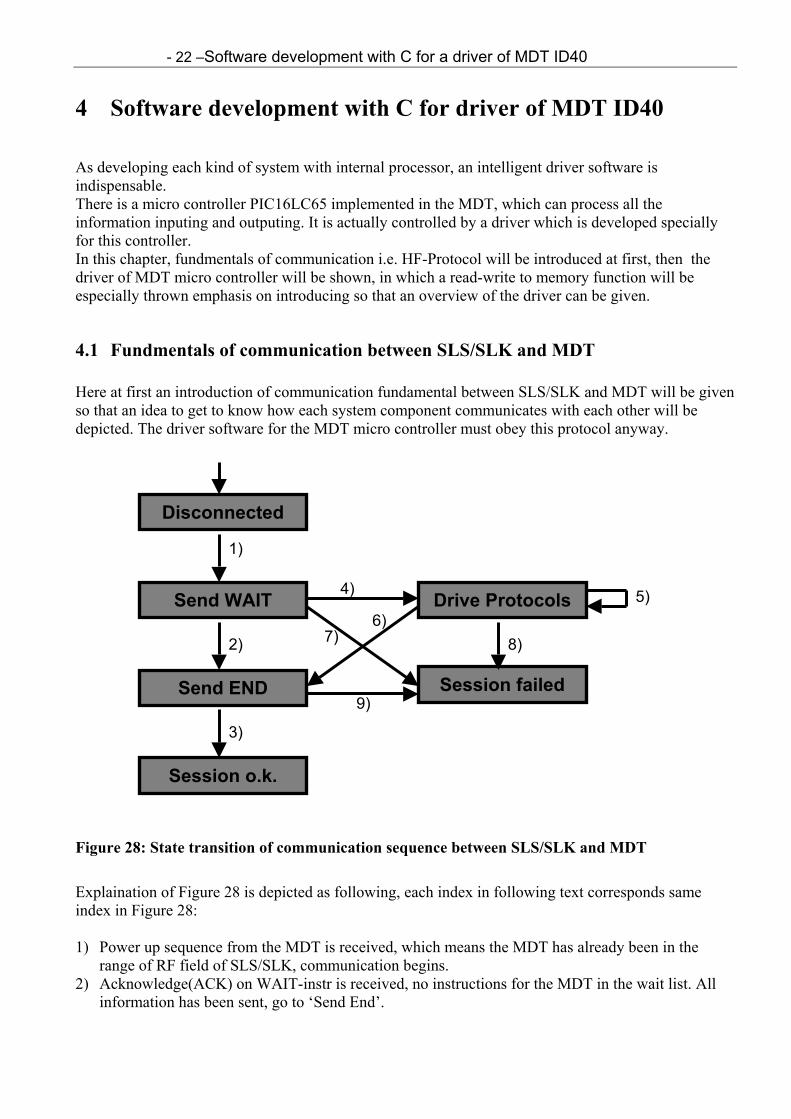
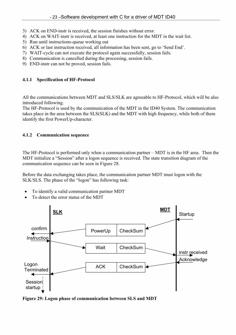
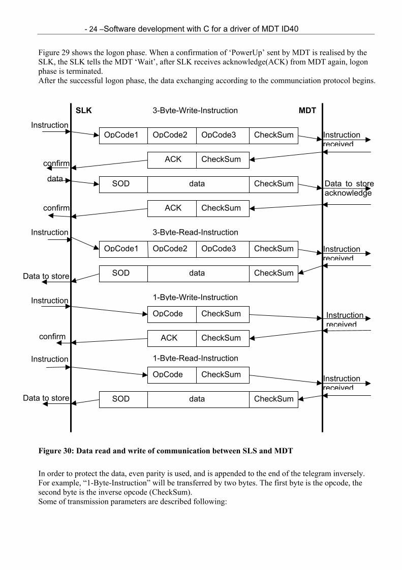
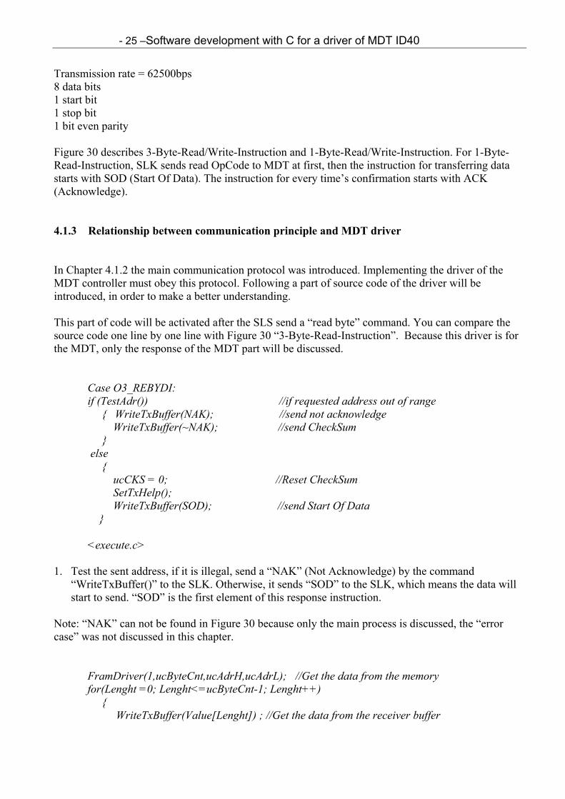
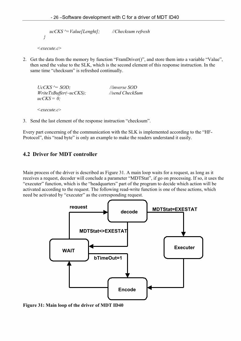
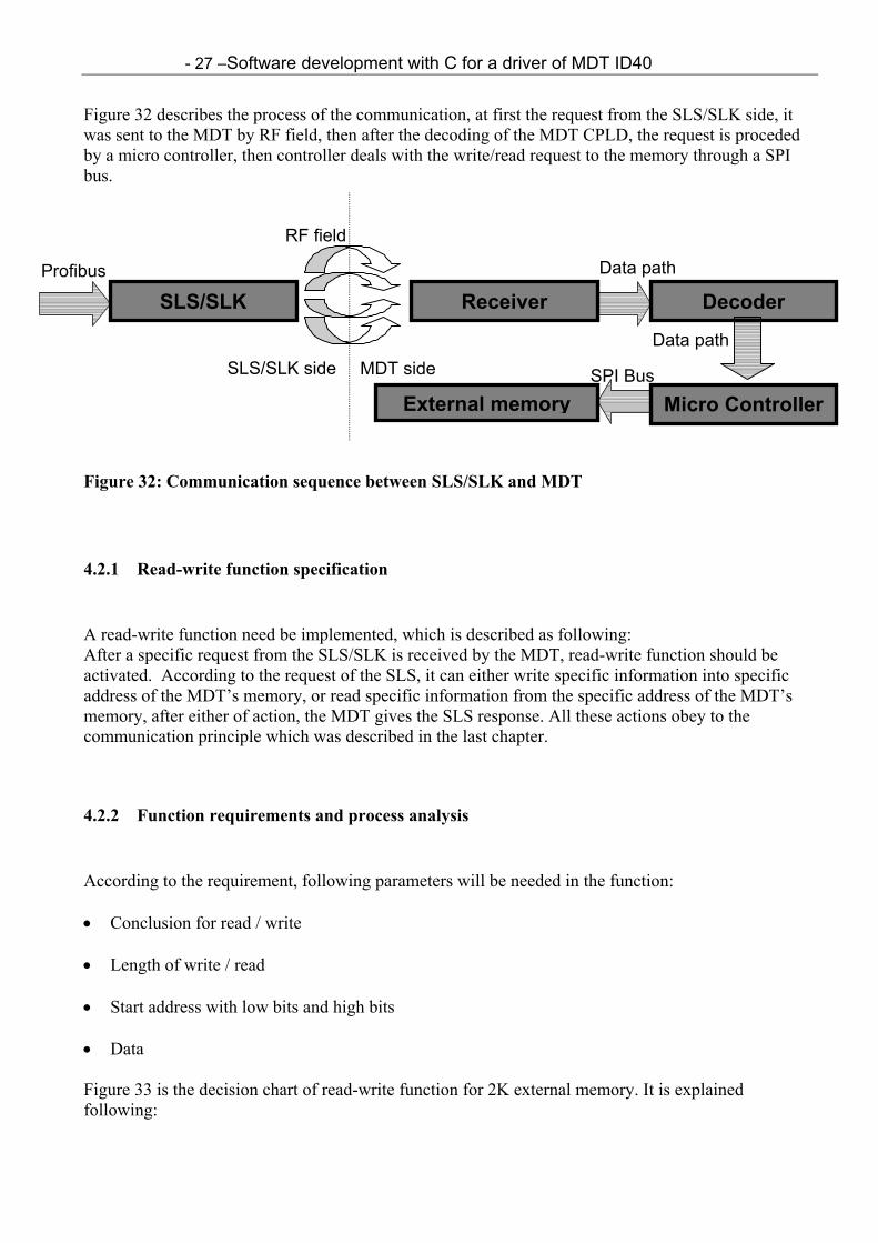
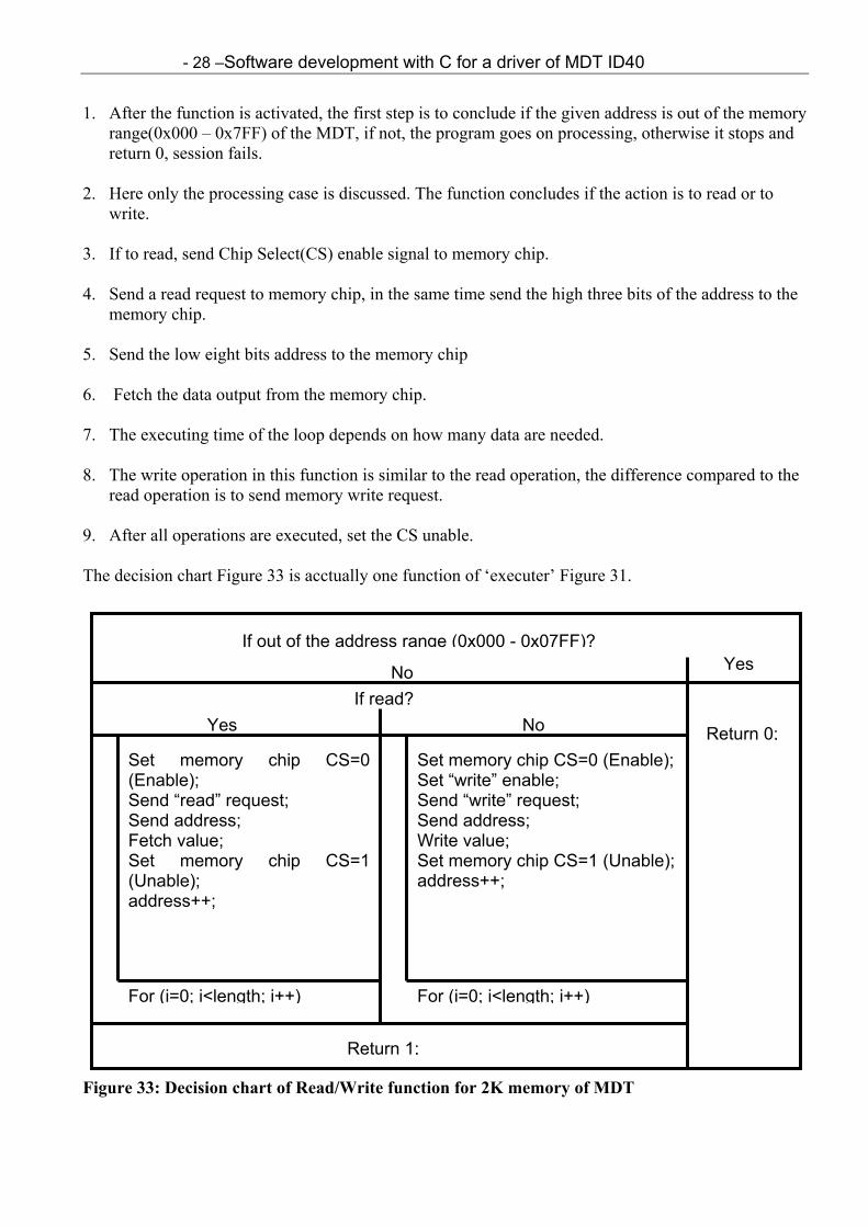
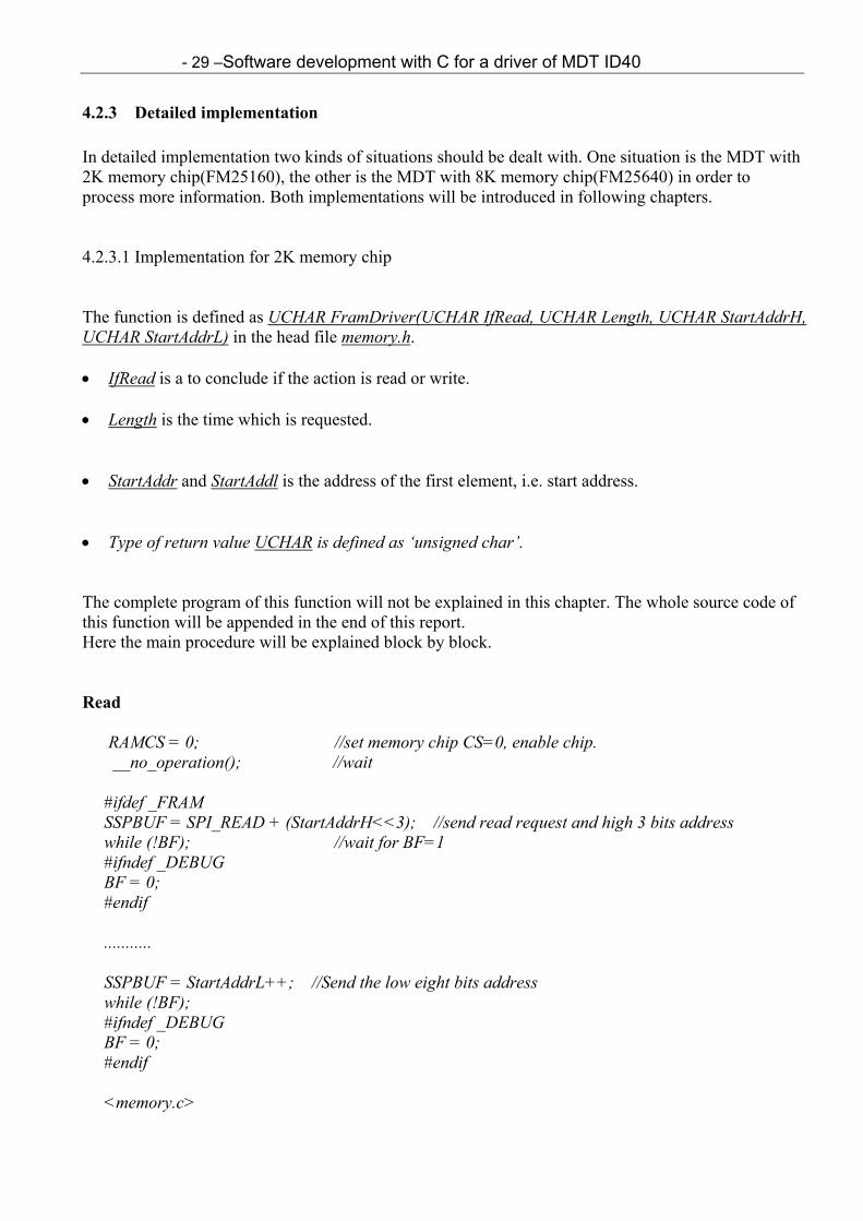
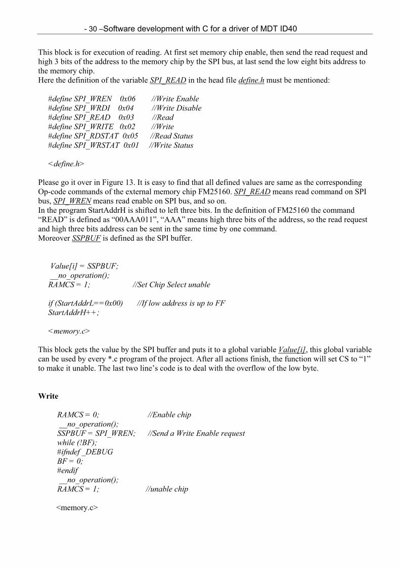
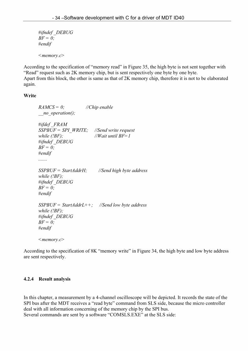
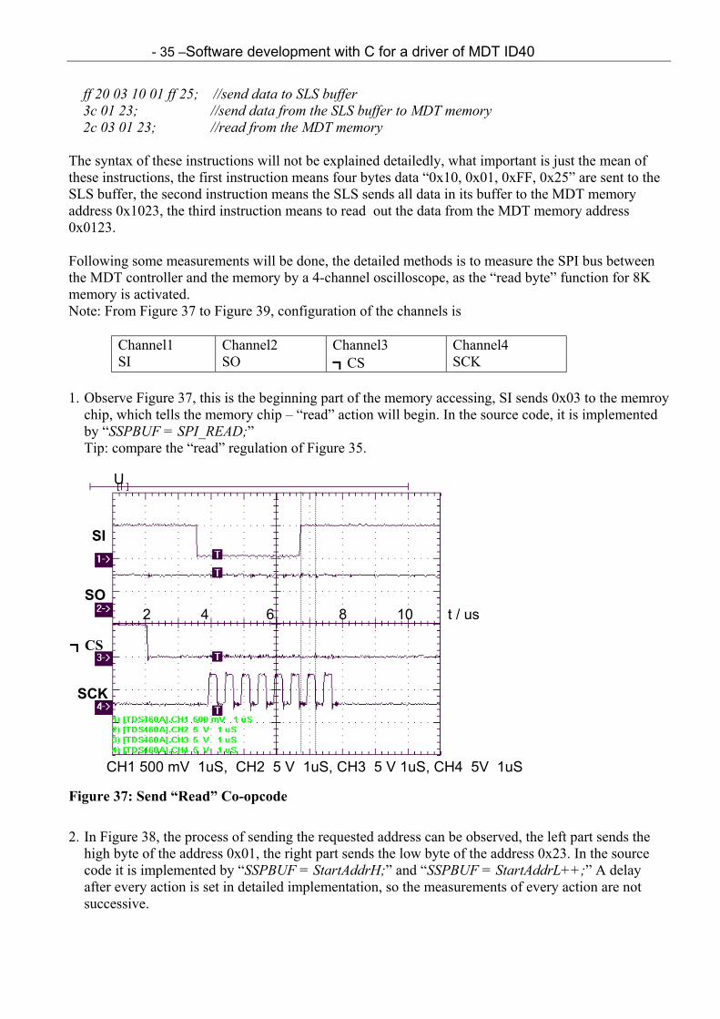
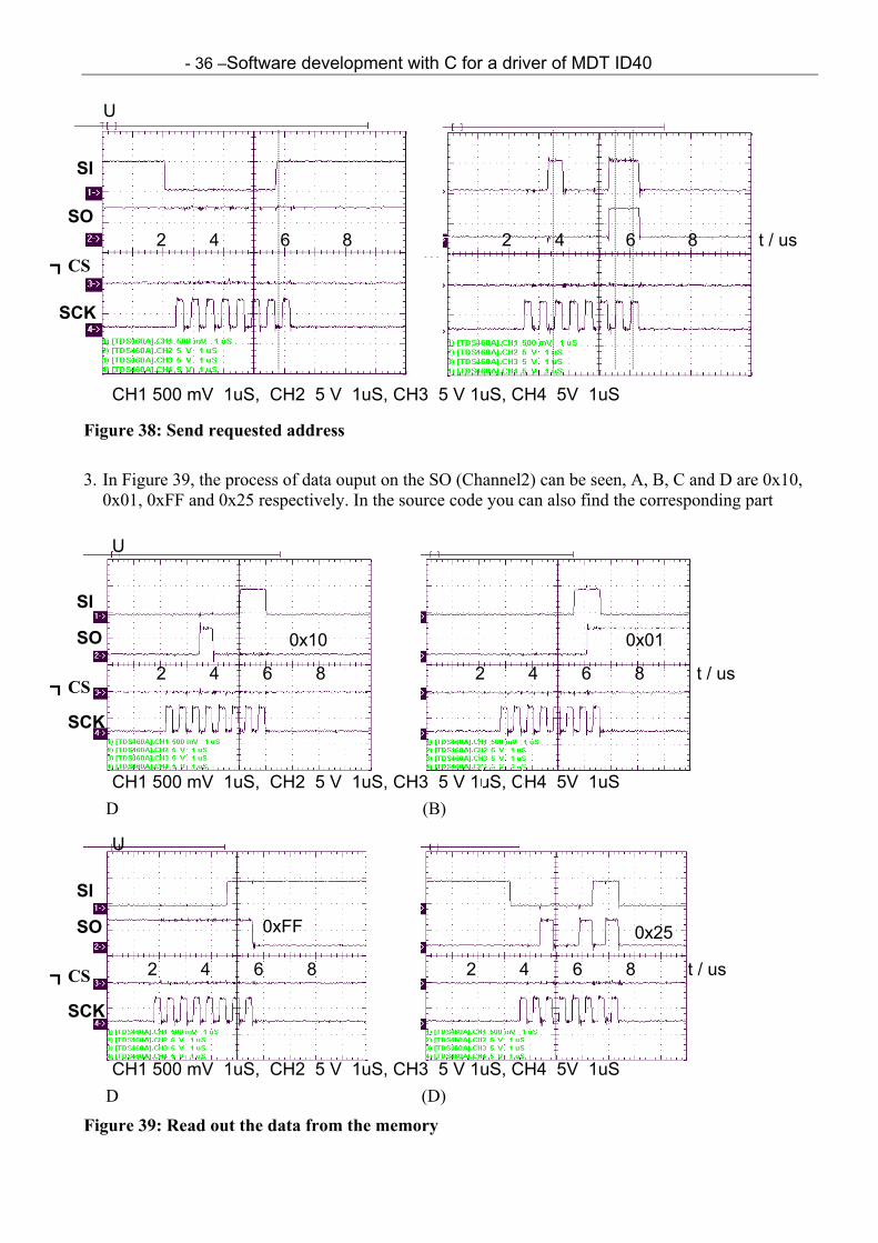

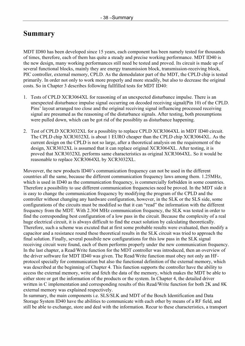

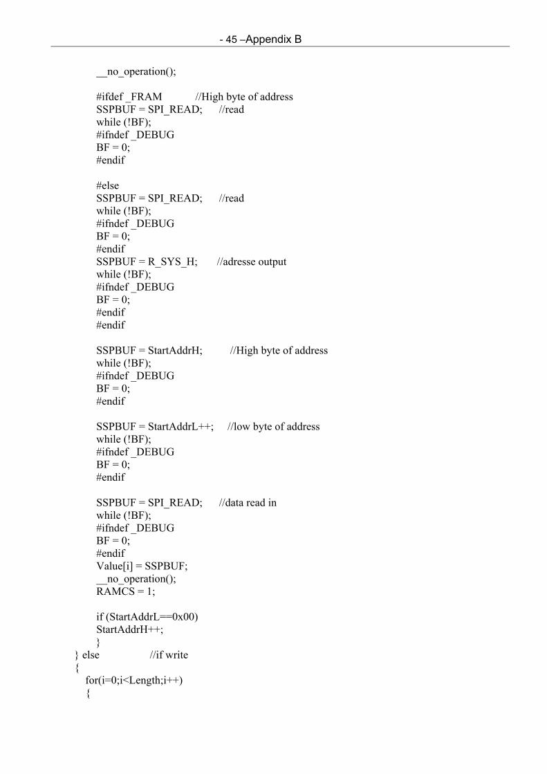
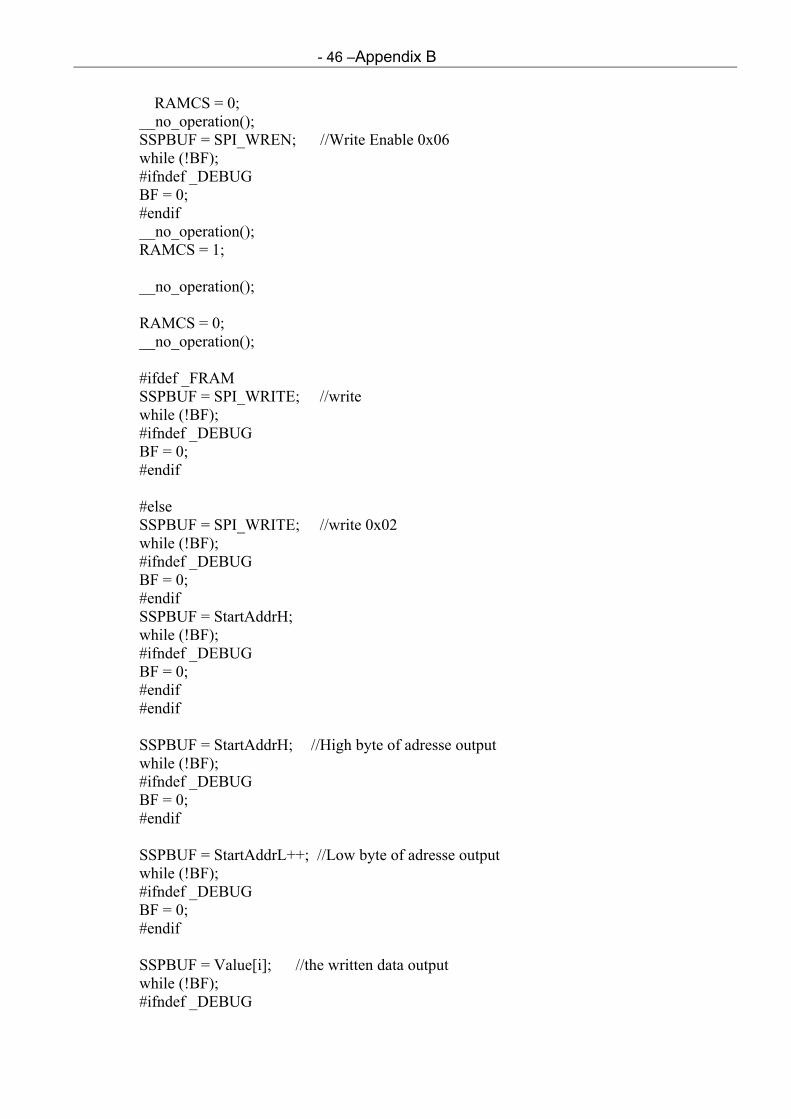
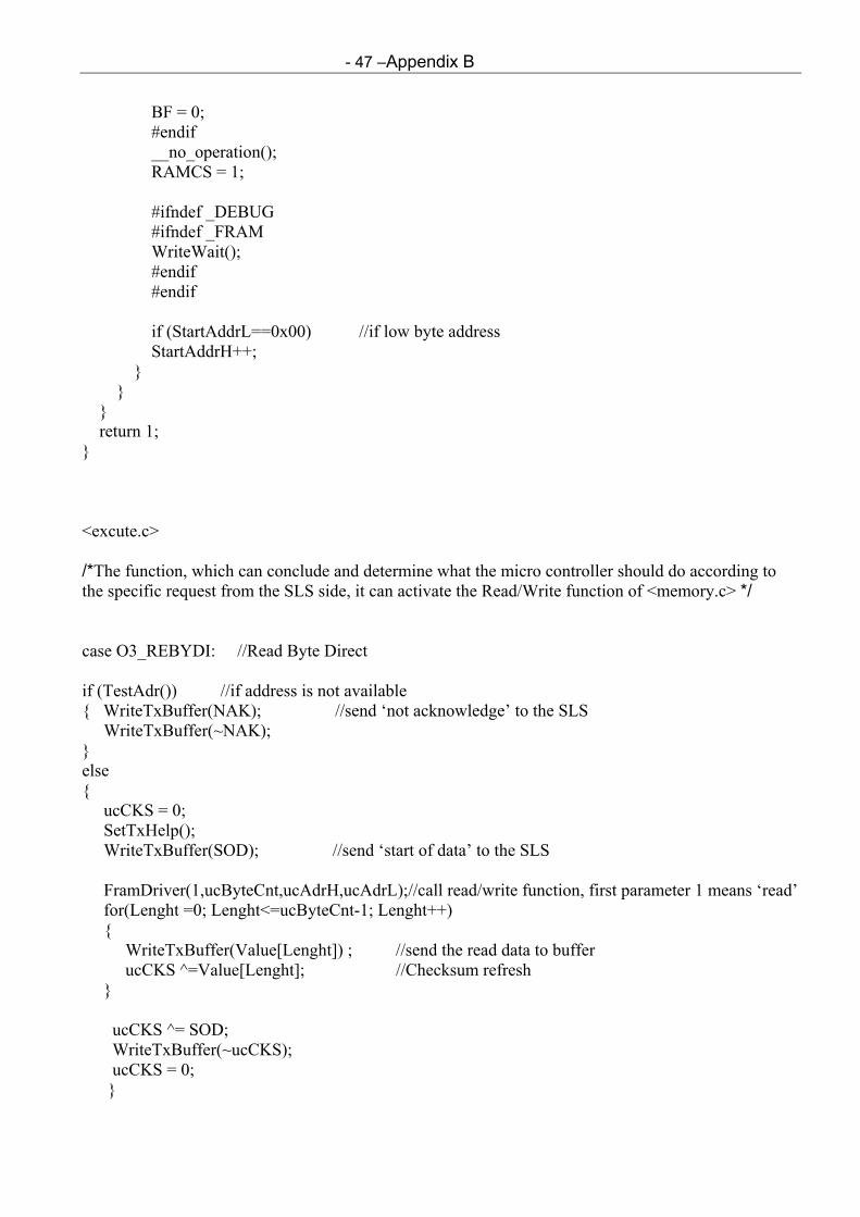
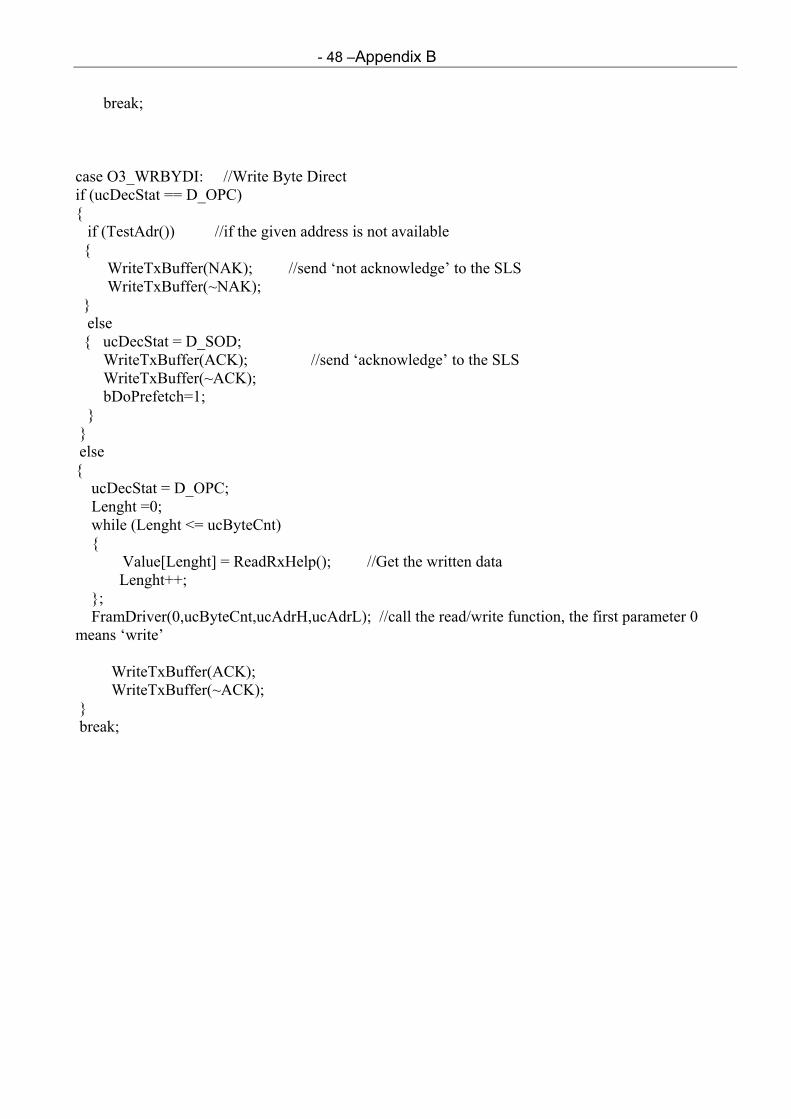


![Präsentation [Schreibgeschützt] [Kompatibilitätsmodus]€¦ · University of Applied Sciences . W, FACHHOCHSCHULE KIEL HOCHSCHULE FOR ANGEWANDTE WISSENSCHAFTEN University of Applied](https://static.documents.pub/doc/80x56/5f1b620b36e9f6320d0622cb/prsentation-schreibgeschtzt-kompatibilittsmodus-university-of-applied.jpg)


