Figure 1: Hierarchy of Non-Volatile Storage How Does Endurance Work in SSDs? Selection of NAND Flash Memory is Critical for Different SSD Applications Solid state drives (SSDs) are mass storage devices for personal, business, scientific, and other applications. They read and write data, and store it in a non-volatile state for future access, use and/or analysis. The heart of the SSD consists of NAND flash memory which utilizes semiconductor cells in its design to store bits of data persistently. When compared to hard disk drives (HDDs), SSDs deliver faster access times, lower latencies, are operationally quieter, and are more resistant to shock and vibration. The NAND flash memory deployed within SSDs represents the most significant cost of all components in a storage system, so keeping it operational through its specified lifetime is both prudent and cost-effective. Understanding the relationship between SSD endurance and NAND flash memory endurance is very important since total cost of ownership (TCO) is tied directly to SSD NAND cost. This brief addresses each and ties the relationship together by including suggestions to improve NAND flash endurance. Along with choices in NAND flash memory, selecting the right one to use for different SSD applications is also presented. SSD Applications SSDs fall into four (4) categories: (1) Storage Class Memory (SCM); (2) Enterprise SSDs; (3) Data Center SSDs; and (4) Client SSDs (Figure 1). A description of each is included (Chart 2): SCM An emerging class of non-volatile memory that bridges the performance gap existing between SSDs and volatile DRAM memory. A wide variety of technologies are being considered for SCM: ReRAM (resistive RAM) FeRAM (ferroelectric RAM) MRAM (magnetic RAM) PCM (phase change memory) Low-latency flash memory SCM acts as non-volatile main memory that is directly accessible by the processor with little to none OS storage stack loading and unloading overhead. It has lower performance and cost when compared to DRAM. Enterprise SSDs For business use within compute servers, All-Flash Arrays (AFAs) and High- Performance Computing (HPC) systems - all of which require very fast data accessibility with the lowest latency. These SSDs service many clients simultaneously and must deliver data access to all without response time degradation. Additional features include robust reliability to support 24 hours by 7 days per week operations, large storage capacities, high endurances and high availability/data protection schemes. Data Center SSDs For business use and targeted to scale-out and hyperscale environments where high performance and tight Quality of Service (QoS) targets are required. These SSDs are optimized for consistent performance and latency, and cost-effectiveness. They do not require a robust enterprise feature set since large data center environments manage data integrity and availability at the node or rack level. Client SSDs For personal use with primary applications that include gaming, online shopping (e-commerce and databases), video/movie streaming, photo taking, and navigation that creates a lot of storage consumption. These SSDs are deployed in personal devices such as smartphones, tablets, digital cameras, and PCs. SSD performance and endurance is subjected to each user’s data consumption Chart 1: Description of Non-Volatile Storage Types Technical Brief
Transcript
Figure 1: Hierarchy of Non-Volatile Storage
How Does Endurance Work in SSDs?Selection of NAND Flash Memory is Critical for Different SSD Applications
Solid state drives (SSDs) are mass storage devices for personal, business, scientific, and other applications. They read and write data, and store it in a non-volatile state for future access, use and/or analysis. The heart of the SSD consists of NAND flash memory which utilizes semiconductor cells in its design to store bits of data persistently. When compared to hard disk drives (HDDs), SSDs deliver faster access times, lower latencies, are operationally quieter, and are more resistant to shock and vibration.
The NAND flash memory deployed within SSDs represents the most significant cost of all components in a storage system, so keeping it operational through its specified lifetime is both prudent and cost-effective. Understanding the relationship between SSD endurance and NAND flash memory endurance is very important since total cost of ownership (TCO) is tied directly to SSD NAND cost. This brief addresses each and ties the relationship together by including suggestions to improve NAND flash endurance. Along with choices in NAND flash memory, selecting the right one to use for different SSD applications is also presented.
SSD ApplicationsSSDs fall into four (4) categories: (1) Storage Class Memory (SCM); (2) Enterprise SSDs; (3) Data Center SSDs; and (4) Client SSDs (Figure 1).
A description of each is included (Chart 2):
SCM
An emerging class of non-volatile memory that bridges the performance gap existing
between SSDs and volatile DRAM memory.
A wide variety of technologies are being considered for SCM: ReRAM (resistive RAM)
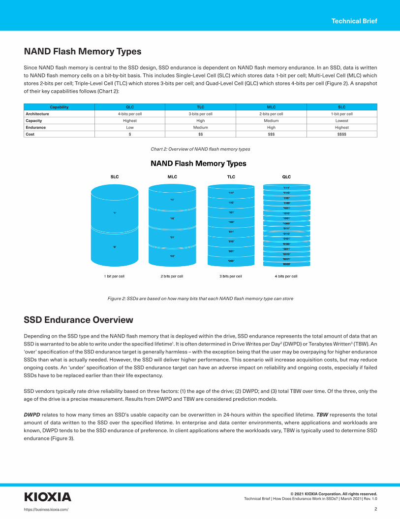
NAND Flash Memory TypesSince NAND flash memory is central to the SSD design, SSD endurance is dependent on NAND flash memory endurance. In an SSD, data is written to NAND flash memory cells on a bit-by-bit basis. This includes Single-Level Cell (SLC) which stores data 1-bit per cell; Multi-Level Cell (MLC) which stores 2-bits per cell; Triple-Level Cell (TLC) which stores 3-bits per cell; and Quad-Level Cell (QLC) which stores 4-bits per cell (Figure 2). A snapshot of their key capabilities follows (Chart 2):
Capability QLC TLC MLC SLCArchitecture 4-bits per cell 3-bits per cell 2-bits per cell 1-bit per cell
Capacity Highest High Medium Lowest
Endurance Low Medium High Highest
Cost $ $$ $$$ $$$$
Chart 2: Overview of NAND flash memory types
Figure 2: SSDs are based on how many bits that each NAND flash memory type can store
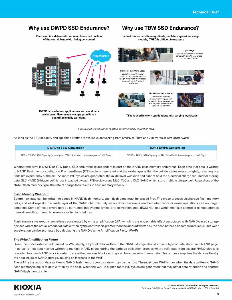
SSD Endurance OverviewDepending on the SSD type and the NAND flash memory that is deployed within the drive, SSD endurance represents the total amount of data that an SSD is warranted to be able to write under the specified lifetime1. It is often determined in Drive Writes per Day2 (DWPD) or Terabytes Written3 (TBW). An ‘over’ specification of the SSD endurance target is generally harmless – with the exception being that the user may be overpaying for higher endurance SSDs than what is actually needed. However, the SSD will deliver higher performance. This scenario will increase acquisition costs, but may reduce ongoing costs. An ‘under’ specification of the SSD endurance target can have an adverse impact on reliability and ongoing costs, especially if failed SSDs have to be replaced earlier than their life expectancy.
SSD vendors typically rate drive reliability based on three factors: (1) the age of the drive; (2) DWPD; and (3) total TBW over time. Of the three, only the age of the drive is a precise measurement. Results from DWPD and TBW are considered prediction models.
DWPD relates to how many times an SSD’s usable capacity can be overwritten in 24-hours within the specified lifetime. TBW represents the total amount of data written to the SSD over the specified lifetime. In enterprise and data center environments, where applications and workloads are known, DWPD tends to be the SSD endurance of preference. In client applications where the workloads vary, TBW is typically used to determine SSD endurance (Figure 3).
Figure 3: SSD endurance is often determined by DWPD or TBW
As long as the SSD capacity and specified lifetime is available, converting from DWPD to TBW, and vice versa, is straightforward:
DWPD to TBW Conversion TBW to DWPD Conversion
TBW = DWPD * SSD Capacity (in terabytes4 (TB)) * Specified Lifetime (in years) * 365 Days DWPD = TBW / {SSD Capacity (in TB) * Specified Lifetime (in years) * 365 Days}
Whether the drive is DWPD or TBW rated, SSD endurance is dependent in part on the NAND flash memory endurance. Each time that data is written to NAND flash memory cells, one Program/Erase (P/E) cycle is generated and the oxide layer within the cell degrades ever so slightly, resulting in a finite life expectancy of the cell. As more P/E cycles are generated, the oxide layer weakens and cannot hold the electrical charge required for storing data. SLC NAND (1-bit per cell) is less impacted by each P/E cycle versus MLC, TLC and QLC NAND which store multiple bits per cell. Regardless of the NAND flash memory type, the rate of charge loss results in flash memory wear-out.
Flash Memory Wear-outBefore new data can be written to pages in NAND flash memory, each flash page must be erased first. The erase process discharges flash memory cells, and as it repeats, the oxide layer of the NAND chip minutely wears down. Failure is reached when write or erase operations can no longer complete. Some of these errors may be corrected, but eventually the error correction code (ECC) routines within the flash controller cannot address them all, resulting in read bit errors or write block failures.
Flash memory wear-out is sometimes accelerated by write amplification (WA) which is the undesirable effect associated with NAND-based storage devices where the actual amount of data written by the controller is greater than the amount written by the host, before it becomes unreliable. This wear acceleration can be estimated by calculating the NAND’s Write Amplification Factor (WAF).
The Write Amplification FactorGiven the undesirable effect caused by WA, ideally, a byte of data written to the NAND storage should equal a byte of data stored in a NAND page. In actuality, that data may be written to multiple NAND pages during the garbage collection process where valid data from several NAND blocks is rewritten to a new NAND block in order to erase the previous blocks so they can be accessible to new data. This process amplifies the data written by the host inside of NAND storage, causing an increase to the WAF. The WAF is the ratio of data written to NAND flash memory versus data written by the host. The most ideal WAF is 1, or when the data written to NAND flash memory is equal to data written by the host. When the WAF is higher, more P/E cycles are generated that may affect data retention and shorten NAND flash memory life.
NAND flash memory endurance can be improved through advanced ECC capabilities that correct common bit errors. The ECC improvements are typically featured in new SSD and NAND flash memory generations developed by vendors. Storage overprovisioning (OP) is the allocation of a predetermined percentage of each SSD’s free space, which is not accessible to the user for maximizing SSD lifetime, endurance or performance.
Selecting the Right NAND Flash Memory for Different SSD ApplicationsFor commercial applications, SSD vendors typically implement NAND flash memory based on supported capacities, and are targeted for general-purpose, mass consumption. KIOXIA America, Inc. offers a variety of SSDs that are available through OEMs, authorized resellers and distributors.
For hyperscalers, computational storage companies, artificial intelligence/machine learning innovators and others who are pushing the boundaries of data storage and building their own specialized storage systems, KIOXIA provides NAND flash memory component solutions.
For these solutions, SSD endurance is aligned to the different NAND flash memory types as follows:
For Client Applications
QLC NAND Flash Memory with DWPD = <0.2TLC NAND Flash Memory with DWPD = <0.3
For Data Center Applications
QLC NAND Flash Memory with DWPD = <0.5 TLC NAND Flash Memory with DWPD = <3
For Enterprise Applications
TLC NAND Flash Memory with DWPD = <3SLC NAND Flash Memory with DWPD > = 10
NOTE: QLC for client and cold storage applications in data center and enterprises, and TLC for client, data center and enterprise NAND component solutions feature KIOXIA’s BiCS FLASH™ 3D flash memory technology. For higher endurance SSD requirements of 10 DWPD or more, SLC floating gate solutions are recommended.
Using computational storage as an example, these vendors require NAND flash memory components to move computations onto SSDs versus host-based processing and disaggregate storage resources from compute resources, making them available to other servers and applications.
SummaryNAND flash memory is the costliest components in a storage system with TCO tied directly to SSD costs. Therefore, SSD vendors, OEM third parties and users have a vested interest in maximizing NAND cell life. SSD endurance has become an important predictive model, often stated in DWPD or TBW, and represents the total amount of data that an SSD is able to write in a specified lifetime. Understanding the ties between NAND flash memory endurance and SSD endurance can help reduce SSD failure rates and unnecessary storage costs. Under-specified endurance targets can have negative effects on drive reliability and ongoing costs, especially if failed SSDs have to be replaced earlier than their life expectancy.
KIOXIA provides a variety of SSD types including NAND flash memory component solutions which enable hyperscalers, server and storage providers, computational storage companies, as well as innovators who build their own specialized storage systems. KIOXIA’s NAND flash memory components take SSD endurance into account - and deliver the right solutions for a variety of SSD applications.
General KIOXIA NAND flash memory information is available here.
1 SSD NAND flash memory will have a different specified lifetime (and associated warranty/warranty period) versus NAND flash memory components (that typically does not fail before their specified lifetime).
2 Drive Write(s) per Day (DWPD): One full drive write per day means the drive can be written and re-written to full capacity once a day, every day, for the specified lifetime. Actual results may vary due to system configuration, usage, and other factors.
3 Terabytes Written (TBW) measures how many cumulative writes that a drive can expect to complete over its lifespan.
4 Definition of capacity - KIOXIA Corporation defines a megabyte (MB) as 1,000,000 bytes, a gigabyte (GB) as 1,000,000,000 bytes and a terabyte (TB) as 1,000,000,000,000 bytes. A computer operating system, however, reports storage capacity using powers of 2 for the definition of 1Gbit = 230 bits = 1,073,741,824 bits, 1GB = 230 bytes = 1,073,741,824 bytes and 1TB = 240 bytes = 1,099,511,627,776 bytes and therefore shows less storage capacity. Available storage capacity (including examples of various media files) will vary based on file size, formatting, settings, software and operating system, and/or pre-installed software applications, or media content. Actual formatted capacity may vary.
TRADEMARKS:
All trademarks or registered trademarks are the property of their respective owners.