How to Design a Thermally-Efficient Integrated BLDC Motor Drive PCB
Application ReportSLVA938A–November 2017–Revised February 2018
How to Design a Thermally-Efficient Integrated BLDCMotor Drive PCB
Cole Macias, David Vaseliou
ABSTRACTThis application report provides an in-depth discussion of thermal design for three-phase integrated BLDCmotor drive PCBs in context of the DRV10987. Theoretical and experimental calculations for junction,ambient, and case temperature are discussed.
1.1 Understanding the Thermal Model ............................................................................... 22 Understanding Sources of Power Dissipation ........................................................................... 2
2.1 RDS(on) ................................................................................................................. 32.2 Switching Loss ...................................................................................................... 32.3 Operating Supply Current Dissipation............................................................................ 32.4 Other Power Dissipation ........................................................................................... 4
3 Understanding Thermal Resistance ....................................................................................... 43.1 Simplified Model .................................................................................................... 43.2 Factors of Junction-to-Case Thermal Resistance (θCA) ........................................................ 5
4 Example Calculations and Data ........................................................................................... 54.1 Power Dissipated Example Calculation ......................................................................... 64.2 Example: Board 1................................................................................................... 74.3 Example: Board 2................................................................................................... 84.4 Test Results Summary ............................................................................................. 8
1 Thermal Model to Electrical Model Schematic........................................................................... 22 Simplified Thermal Resistance Model for a Typical PCB .............................................................. 43 Expanded Thermal Resistance Model for a Typical PCB ............................................................. 54 Board 1 Thermal Image for Top of Case Temperature ................................................................ 75 Board 2 Thermal Image for Top of Case Temperature ................................................................ 86 Thermal Simulation Data Comparing Board Size and Copper Weight.............................................. 107 Hot Spot Created When a Break is Created in the Thermal Path ................................................... 11
How to Design a Thermally-Efficient Integrated BLDC Motor Drive PCB
1 IntroductionFor BLDC motor drive applications, temperature is often a critical design specification that cannot beviolated. Specifically, cooling applications such as pedestal fans, ceiling fans, HVAC automotive seatblowers, washer and dryer fans, server fans, and refrigerator fans should try to dissipate heat as efficientlyas possible. This allows for the lowest possible ambient (TA) and case (TC) temperature, in addition to, thelowest possible silicon die or junction temperature (TJ) inside the device package. As previouslymentioned, these temperatures are important because the ambient, case, and junction temperatures linkto critical design specifications.
For the ambient and case temperature, the design specifications are often determined by the application.For example, dryer units deal with very hot ambient temperatures and a dryer fan motor drive circuitproduces extra heat that contributes to the overall ambient temperature. As a result, a system used in ahome-appliance dryer might design a dryer system that should not violate an ambient temperature of65°C. In addition, some applications might have heat sensitive material (that is, waterproofing sealant) inclose proximity to the motor drive circuits that are disrupted if the case temperature exceeds a certaintemperature.
For junction temperature, many devices will not operate correctly if the minimum or maximum junctiontemperature specifications are violated. For example, the DRV10987 has a maximum junction temperatureof 150°C in the absolute maximum ratings table of DRV10987 12- to 24-V, Three-Phase, SensorlessBLDC Motor Driver . While the DRV10987 has overtemperature protection that shuts down the device, thisdoes not excuse good design practices which could prevent the overtemperature condition from occurring.In addition, motor drive applications are driven by design specifications such as output current. Since thecurrent is directly correlated to the power dissipated, increasing the junction temperature, better thermaldesign allows for higher current with the same temperature.
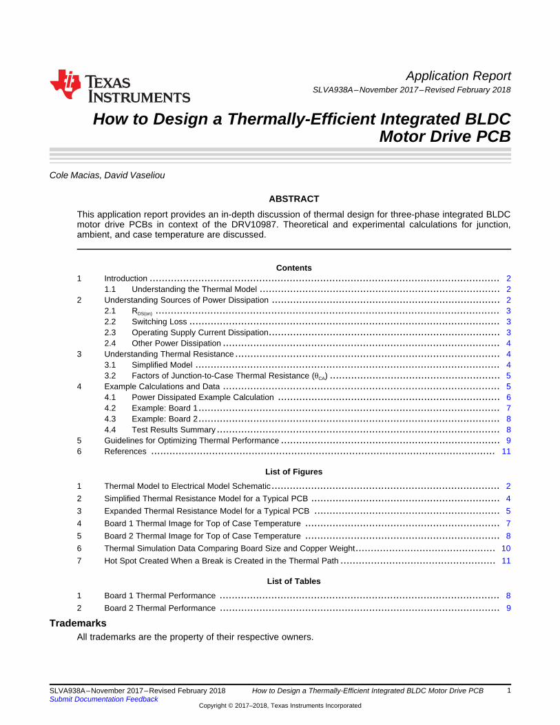
1.1 Understanding the Thermal ModelHeat dissipation on a printed circuit board (PCB) can be broken down into a simple model that closelyresembles the electrical circuit model. Specifically, the electrical circuit model is broken down to voltage(V), current (I), and resistance (R) through a simple relationship shown in Equation 1:
(1)
The thermal model takes temperature (T), power dissipation (P), and thermal resistance (θ) and relatesthem to voltage, current, and resistance, respectively. This is shown in Equation 2.
(2)
Figure 1. Thermal Model to Electrical Model Schematic
In Figure 1, the thermal model is represented in a schematic format to illustrate the typical conventionsestablished by electrical circuit modeling. Since the ambient and junction temperature are represented asvoltages, their difference is simply the sum of all dissipated power times the thermal resistance betweenthe silicon die and the ambient air. This is represented in Equation 3.
(3)
2 Understanding Sources of Power DissipationSince there are multiple sources of power dissipation in a BLDC motor driver, their sum results in the totalpower dissipated in the circuit. This is used to calculate the junction temperature. While a short descriptionis provided for each source of power dissipation, more information is found in Calculating Motor DriverPower Dissipation .
Equation 4 summarizes all sources of power dissipation.(4)
How to Design a Thermally-Efficient Integrated BLDC Motor Drive PCB
2.1 RDS(on)
The largest source of dissipated power inside a three-phase BLDC motor driver is the current flowingthrough the power MOSFETs. When the FETs are turned on, the high- and low-side FETs act as resistors(RDS(on)) that allow the current to flow from the supply to the terminal windings of the motor. The act ofcurrent flowing through the windings is what causes a magnetic field to develop and attract the permanentmagnets on the rotor to cause motion. The power dissipated is represented by Equation 5.
(5)
Where:• RDS(on) = sum of RDS(on) for both the high- and low-side FETs• IOUT(RMS) = RMS output current being applied to the motor windings (not to be confused with the supply
current)
Since RDS(on) increases as temperature increases, note that the lower the junction temperature and powerdissipation from the FETs reduces the power dissipated.
In the case of the DRV10987, the typical RDS(on) at TA = 25°C is 425 mΩ and the maximum continuouscurrent is 2 A(RMS). Since the DRV10987 is a three-phase BLDC motor driver with 180° sinusoidal control,all of the power MOSFETs and phase terminal windings have current flowing through them duringoperation. The sum of the phase shifted sinusoidal current waveforms equate to a constant powerdissipation.
2.2 Switching LossFor a three-phase BLDC driver, switching loss refers to the power dissipated when a transistor switchesfrom high to low and low to high. Since three-phase BLDCs are controlled with PWM signals on the gatesof the power MOSFETs, some power is dissipated every time the switching occurs. This is represented inEquation 6.
(6)
Where:• VM = supply voltage that is supplied to motor, otherwise known as motor voltage• IOUT(RMS) = RMS output current being applied to the motor windings (not to be confused with the supply
current)• fSW = switching frequency of the PWM signal• SR = slew rate of the switching signal.
The DRV10987 has a maximum output current of 2 A(RMS) and can operate with a supply voltage from 6.2V to 28 V. The PWM switching frequency is configured for 25 kHz or 50 kHz and the slew rate can beconfigured for 120, 80, 50, or 35 V/µs.
2.3 Operating Supply Current DissipationThe driver consumes some current during operation. Note that the absence of a speed command canplace the devices into sleep or standby to minimize current. However, the power dissipated calculationsonly rely on operation conditions. This is shown in Equation 7:
(7)
Where:• VM = supply voltage that is supplied to motor, otherwise known as motor voltage• IVCC = active current during operation
The DRV10987 uses the specification called active current to quantify the amount of supply currentconsumed during operation. Note that the DRV10987 includes a step-down hysteretic voltage regulatorthat can operate with an external inductor or resistor. Depending on the component and mode used in thedesign, the active current is defined differently. Consult DRV10987 12- to 24-V, Three-Phase, SensorlessBLDC Motor Driver in the step-down regulator section for more information.
How to Design a Thermally-Efficient Integrated BLDC Motor Drive PCB
The typical value of the active current in the resistor mode is 13 mA, the maximum value is 16 mA.
2.4 Other Power DissipationMany motor drivers, including the DRV10987, have an LDO regulator that provides some current. TheLDO offered on the DRV10987 outputs 3.3 V and more information is found in DRV10987 12- to 24-V,Three-Phase, Sensorless BLDC Motor Driver . This is represented in Equation 8:
(8)
Where:• ILDO_OUT = output current from the LDO with load• VM = supply voltage that is supplied to motor, otherwise known as motor voltage• VOUT = output voltage of the LDO
If the LDO is not outputting any current, ignore this power dissipation.
3 Understanding Thermal ResistanceFor many semiconductor devices, the junction-to-thermal resistance is often given as a specification in thedata sheet. For example, the DRV10987 shows θJA is 36.1 °C/W. While this specification is based on dataand JEDEC standards, the junction-to-thermal resistance does not account for real world factors and goodthermal design like board thickness, use of a die attach pad (DAP) or power pad, copper thickness, vias,and breaks in the thermal path. These factors can reduce the thermal resistance making it easier for heatto uniformly dissipate and reduce the junction temperature.
3.1 Simplified Model
Figure 2. Simplified Thermal Resistance Model for a Typical PCB
As Figure 2 illustrates, the thermal model shows that the junction-to-ambient thermal resistance is but onecomponent. However, the thermal resistance can be broken up into multiple parallel paths that make up allof the thermal resistance. In this case, a simplified version of the model is used.
Figure 2 shows that there are two paths for heat to travel from the junctions of the silicon: up towards thetop of the case and down towards the power pad through the bottom of the PCB. This equivalent thermalresistance is found in Equation 9:
(9)
Where:• θJT = junction-to-case (top) thermal resistance• θTA = case (top) to ambient thermal resistance• θJC = junction-to-case (power pad or equivalent path of least resistance) thermal resistance• θCA = case (power pad or equivalent path of least resistance) to ambient thermal resistance (through
How to Design a Thermally-Efficient Integrated BLDC Motor Drive PCB
Equation 9 describes an important relationship for identifying the thermal resistance of the system. θJT, θTA,and θJC are all fixed values that cannot be influenced by the designer. However, θCA can be greatlyreduced applying good thermal design. Since the paths to the top and bottom of the case are in parallel, ifthe θCA is reduced to a small enough value, ignore the path to the top of the case.
NOTE: θJT, θTA, and θJC are all values that are widely known or found in the data sheet where θCA iscalculated.
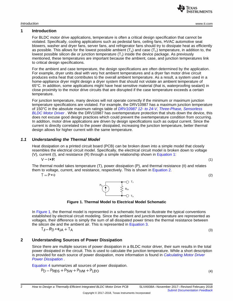
3.2 Factors of Junction-to-Case Thermal Resistance (θCA)As Figure 3 shows, there are many paths for heat to travel: through the copper plane laterally, verticallythrough thermal vias, through the vertical FR-4 laminate of the PCB, and radiating off the surface of theboard to the ambient air. These paths are broken into parallel paths where the thermal resistance varies.As previously mentioned, it is important to make every path low resistance. As a result, higher resistancepaths such as paths using the FR-4, contribute less to the overall θCA.
Figure 3. Expanded Thermal Resistance Model for a Typical PCB
While these thermal resistances are modeled like resistors in an electrical circuit model, the modeledresistor network is complicated and may not perfectly model the board. Generally, vias and copper planeshave a lower thermal resistance than the FR-4 laminate of the PCB. Equations and typical values forthese factors are found in AN-2020 Thermal Design By Insight, Not Hindsight . However, the effects ofthese equations are summarized into general guidelines and design rules in Section 5 with supportingdata in Section 4.
NOTE: A useful θ CA and θJA can be obtained through thermal modeling PCB simulation software.However, this modeling is usually provided as a service and associated as an extra costduring production.
4 Example Calculations and DataBefore showing the typical calculations and data collection used in thermal analysis, the methods forfinding the junction temperature must be discussed.
(10)
As previously mentioned, Equation 10 shows the very inaccurate and rough measurement that is typicallyused to calculate the junction temperature. This method does not take into account the effects of goodthermal PCB design.
How to Design a Thermally-Efficient Integrated BLDC Motor Drive PCB
Where:• ΨJT = junction to top of case characterization parameter• TC = temperature at the top of the case
Equation 11 illustrates how junction temperature is calculated when measuring the temperature at the topof the case. Using the measured temperature at the top of the case and power dissipation, thecharacterization parameter ΨJT is taken from the data sheet to calculate the junction temperature.
While θJT is often confused for ΨJT when doing the calculation, the use of junction to top of case thermalresisitance, θJT, only works in context of Equation 9 and the modeling of the parallel paths discussed inSection 3.1 and Section 3.2.
The characterization parameter ΨJT is based on widely-adopted standards (JEDEC51-2). Furthermore, ΨJTestimates junction temperature based on experimental data instead of theoretical modeling. As a result,use ΨJT when the actual case temperature is measured. More information is found in Semiconductor andIC Package Thermal Metrics .
Note that the JEDEC standards were developed to help standardize sizes and layout for testing thermalmetrics in most data sheets. Look for the verbiage indicating JEDEC standards when evaluating thermalmetrics between different devices.
4.1 Power Dissipated Example CalculationAssumptions for calculations are based on measured or typical and maximum electrical characteristicvalues:• Two boards with two different devices were tested using the same HSOP package size to minimize
thermal resistance error.• Board 1 was not optimized for thermal performance where board 2 was optimized.• Board 1 had a one-oz copper pour while board 2 had a two-oz copper pour.• VCC = 19.6 V and TA_Measured = 24°C.• For simplicity, IOUT(RMS) = 2.9 A(RMS) for both boards despite IOUT(RMS)-Board1 = 2.85 A(RMS) and IOUT(RMS)-Board2 =
2.95 A(RMS). This introduces some error in favor of board 2.• RDS(on) value assumes TA = 25°C where TA_Measured = 24°C. This will introduce some error for both
boards.• Slew rate (SR) was set to 35 V/µs and the PWM frequency was set to 25 kHz.• Both boards were in inductor mode. The maximum specification (15 mA) was used for margin.• The LDO had no load in both experiments.• The same motor was used with both boards in same environment to minimize error.
Calculating PRDS, more information is available in Section 2.1. Note 250 mΩ is the typical value for RDS(on)at TA = 25°C, as mentioned in the assumptions:
(12)
Calculating PSW, more information is available in Section 2.2:
(13)
Calculating PIVM, more information is available in Section 2.3:
How to Design a Thermally-Efficient Integrated BLDC Motor Drive PCB
(14)
Calculating PLDO_OUT, more information is available in Section 2.4:
(15)
Calculating PD:
(16)
This value is used to calculate TJ.
4.2 Example: Board 1To estimate the junction temperature (TJ) of the device, we use both Equation 10 and Equation 11. Aspreviously mentioned, Equation 10 is inaccurate as an estimation. In the previous section we calculatedthe power dissipated on board 1 as 4.244 W. From the data sheet, θJA is 36.1°C/W and the ΨJT is0.4°C/W. We use the measured value (157.5°C) of the top-of-case temperature when the device isdissipating 4.244 W for TC. Figure 4 shows the measured top-of-case temperature for board 1.
(17)
Where:• TA = ambient temperature• TJ = junction temperature• PD= power dissipated• θJA = junction-to-ambient thermal resistance
(18)
Figure 4. Board 1 Thermal Image for Top of Case Temperature
How to Design a Thermally-Efficient Integrated BLDC Motor Drive PCB
4.3 Example: Board 2As with board 1, solving for TJ with the same power dissipation at the same ambient temperature, thejunction temperature equals 291.07°C. This is because Equation 10 does not take into account PCBlayout thermal techniques.
As for Equation 11, the only change is the measured T C which is caused by thermal optimizationtechniques. Figure 5 shows the Top of Case temperature for Board 2.
(19)
Figure 5. Board 2 Thermal Image for Top of Case Temperature
4.4 Test Results SummaryTable 1 and Table 2 show the measured thermal performance of board 1 and board 2, respectively.
Table 1. Board 1 Thermal Performance
Speed (RPM) I RMS (A) Voltage Top of Case Temperature (°C) Power (W)6090 1.88 19.65 71.8 36.9426420 2.05 19.6 79.1 40.186750 2.24 19.6 84.7 43.9047140 2.4 19.64 91.8 47.1367410 2.54 19.57 103.4 49.70787800 2.68 19.6 118.0 52.5288190 2.78 19.6 132.4 54.4888460 2.85 19.6 157.5 55.86
How to Design a Thermally-Efficient Integrated BLDC Motor Drive PCB
Table 2. Board 2 Thermal Performance
Speed (RPM) I RMS (A) Voltage Top of Case Temperature (°C) Power (W)6150 1.52 19.57 53.8 29.7466540 1.66 19.64 57.3 32.6026930 1.824 19.63 61.9 35.80517230 1.975 19.55 67.1 38.6117650 2.12 19.56 74.7 41.4678010 2.24 19.57 81.4 43.8378220 2.38 19.57 91.3 46.5778490 2.54 19.55 102.6 49.6578820 2.65 19.5 115.9 51.6759150 2.78 19.43 123.4 54.01549330 2.95 19.41 139.1 57.3189570 3.075 19.41 144.1 59.686
As the calculated and measured results show, using good thermal optimization layout techniques providessignificant improvements in thermal performance allowing for better efficiency and higher powerconsumption while driving a motor. The calculations also show how using Equation 10 can be inaccuratefor estimating a junction temperature far greater than the thermal shutdown temperature. UsingEquation 11 is a better estimate for the junction temperature resulting in a realistic junction temperature.
5 Guidelines for Optimizing Thermal PerformanceUse the following recommendations as guidelines for designing the PCB for thermal testing or functionalevaluation:• Use a large and multi-layer PCB:
– Use Equation 20 to find the minimum recommended board size if θJC is unknown:
(20)– Use Equation 21 to find minimum recommended board size if θJC is known:
(21)• TI recommends using at least one-oz copper.
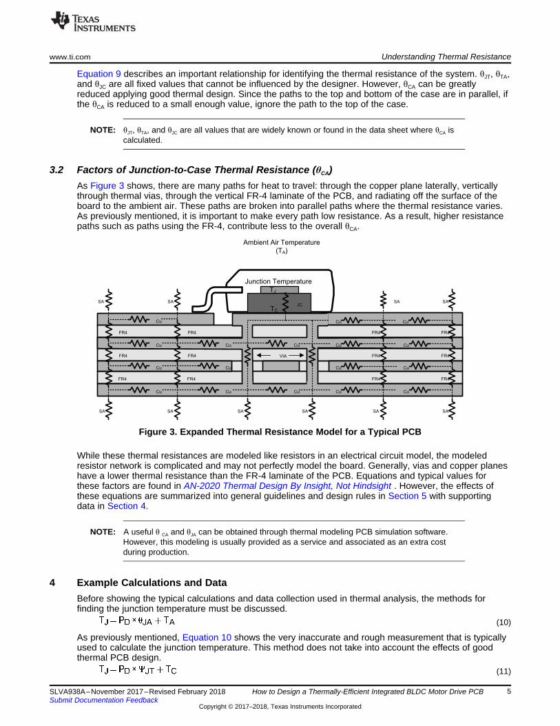
– Two-oz copper is recommended for designs that dissipate more than 3 W.– Four-oz copper is recommended for designs that dissipate more than 6 W.– Figure 6 shows the affects of board size and copper weight on thermal performance.
How to Design a Thermally-Efficient Integrated BLDC Motor Drive PCB
Figure 6. Thermal Simulation Data Comparing Board Size and Copper Weight
• Use thermal vias connecting the DAP landing pattern on the top layer, inter GND, and bottom GNDlayer in both DAP landing pattern and ground plane.– Use Equation 22 to find the thermal resistance of vias.
(22)• Design the thermal vias near the periphery of the exposed DAP if the maximum number of vias is not
applicable.• Use 0.33-mm diameter vias if possible, especially for packages with small exposed pad, which may
reduce θJA approximately 15% to 25%.• Generate as large a GND plane as allowable on the top and bottom layers, especially near the
package.– Generate with as few breaks as possible to create a heat spreader on the PCB.
• Connect the top GND pattern with the DAP landing pattern underneath the package.• Gather the same functional pins together in die design, such as for GND, PVIN, POUT in the power
device. This allows maximizing the Cu area near the package by eliminating the needs for isolatingeach lead pattern on the PCB.
• Make the traces as long as possible, achieving better thermal conductivity near the package.• Do not run traces parallel to the board edge, this blocks thermal path edges of the board
Figure 7. Hot Spot Created When a Break is Created in the Thermal Path
6 References1. DRV10987 Product Folder: http://www.ti.com/product/DRV109872. Texas Instruments, Calculating Motor Driver Power Dissipation Application Report3. Texas Instruments, AN-2020 Thermal Design By Insight, Not Hindsight Application Report4. Texas Instruments, Semiconductor and IC Package Thermal Metrics Application Report
Revision HistoryNOTE: Page numbers for previous revisions may differ from page numbers in the current version.
Changes from Original (November 2017) to A Revision ................................................................................................ Page
• Changed Equation 5. ..................................................................................................................... 3• Added thermal modeling PCB simulation software note. ............................................................................ 5• Added last bullet in the Power Dissipated Example Calculation section. .......................................................... 6• Changed Equation 12..................................................................................................................... 6• Changed Equation 13..................................................................................................................... 6• Changed 7.398 W to 4.244 W in the Example: Board 1 section and made appropriate equation changes. ................. 7• Changed Equation 18..................................................................................................................... 7• Changed Equation 19..................................................................................................................... 8
IMPORTANT NOTICE FOR TI DESIGN INFORMATION AND RESOURCES
Texas Instruments Incorporated (‘TI”) technical, application or other design advice, services or information, including, but not limited to,reference designs and materials relating to evaluation modules, (collectively, “TI Resources”) are intended to assist designers who aredeveloping applications that incorporate TI products; by downloading, accessing or using any particular TI Resource in any way, you(individually or, if you are acting on behalf of a company, your company) agree to use it solely for this purpose and subject to the terms ofthis Notice.TI’s provision of TI Resources does not expand or otherwise alter TI’s applicable published warranties or warranty disclaimers for TIproducts, and no additional obligations or liabilities arise from TI providing such TI Resources. TI reserves the right to make corrections,enhancements, improvements and other changes to its TI Resources.You understand and agree that you remain responsible for using your independent analysis, evaluation and judgment in designing yourapplications and that you have full and exclusive responsibility to assure the safety of your applications and compliance of your applications(and of all TI products used in or for your applications) with all applicable regulations, laws and other applicable requirements. Yourepresent that, with respect to your applications, you have all the necessary expertise to create and implement safeguards that (1)anticipate dangerous consequences of failures, (2) monitor failures and their consequences, and (3) lessen the likelihood of failures thatmight cause harm and take appropriate actions. You agree that prior to using or distributing any applications that include TI products, youwill thoroughly test such applications and the functionality of such TI products as used in such applications. TI has not conducted anytesting other than that specifically described in the published documentation for a particular TI Resource.You are authorized to use, copy and modify any individual TI Resource only in connection with the development of applications that includethe TI product(s) identified in such TI Resource. NO OTHER LICENSE, EXPRESS OR IMPLIED, BY ESTOPPEL OR OTHERWISE TOANY OTHER TI INTELLECTUAL PROPERTY RIGHT, AND NO LICENSE TO ANY TECHNOLOGY OR INTELLECTUAL PROPERTYRIGHT OF TI OR ANY THIRD PARTY IS GRANTED HEREIN, including but not limited to any patent right, copyright, mask work right, orother intellectual property right relating to any combination, machine, or process in which TI products or services are used. Informationregarding or referencing third-party products or services does not constitute a license to use such products or services, or a warranty orendorsement thereof. Use of TI Resources may require a license from a third party under the patents or other intellectual property of thethird party, or a license from TI under the patents or other intellectual property of TI.TI RESOURCES ARE PROVIDED “AS IS” AND WITH ALL FAULTS. TI DISCLAIMS ALL OTHER WARRANTIES ORREPRESENTATIONS, EXPRESS OR IMPLIED, REGARDING TI RESOURCES OR USE THEREOF, INCLUDING BUT NOT LIMITED TOACCURACY OR COMPLETENESS, TITLE, ANY EPIDEMIC FAILURE WARRANTY AND ANY IMPLIED WARRANTIES OFMERCHANTABILITY, FITNESS FOR A PARTICULAR PURPOSE, AND NON-INFRINGEMENT OF ANY THIRD PARTY INTELLECTUALPROPERTY RIGHTS.TI SHALL NOT BE LIABLE FOR AND SHALL NOT DEFEND OR INDEMNIFY YOU AGAINST ANY CLAIM, INCLUDING BUT NOTLIMITED TO ANY INFRINGEMENT CLAIM THAT RELATES TO OR IS BASED ON ANY COMBINATION OF PRODUCTS EVEN IFDESCRIBED IN TI RESOURCES OR OTHERWISE. IN NO EVENT SHALL TI BE LIABLE FOR ANY ACTUAL, DIRECT, SPECIAL,COLLATERAL, INDIRECT, PUNITIVE, INCIDENTAL, CONSEQUENTIAL OR EXEMPLARY DAMAGES IN CONNECTION WITH ORARISING OUT OF TI RESOURCES OR USE THEREOF, AND REGARDLESS OF WHETHER TI HAS BEEN ADVISED OF THEPOSSIBILITY OF SUCH DAMAGES.You agree to fully indemnify TI and its representatives against any damages, costs, losses, and/or liabilities arising out of your non-compliance with the terms and provisions of this Notice.This Notice applies to TI Resources. Additional terms apply to the use and purchase of certain types of materials, TI products and services.These include; without limitation, TI’s standard terms for semiconductor products http://www.ti.com/sc/docs/stdterms.htm), evaluationmodules, and samples (http://www.ti.com/sc/docs/sampterms.htm).