June 2009 Doc ID 14614 Rev 2 1/24 PM0051 Programming manual How to program STM8S Flash program memory and data EEPROM Introduction This manual describes how to program Flash program memory and data EEPROM on STM8 microcontrollers. It applies to STM8S access and performance line family of devices. It is intended to provide information to the programming tool manufacturers and to the customers who want to implement programming by themselves on their production line. The in-circuit programming (ICP) method is used to update the content of Flash program memory and data EEPROM while the user software is not running. It uses the Single wire interface module (SWIM) to communicate between the programming tool and the device. In contrast to the ICP method, in-application programming (IAP) can use any communication interface supported by the microcontroller (I/Os, SPI, USART, SCI, USB, CAN...). IAP has been implemented for users who want their application software to update itself by re-programming the Flash program memory during program execution. The main advantage of IAP is its ability to re-program Flash program memory and data EEPROM when the chip has already been soldered on the application board and while the user software is running. Nevertheless, part of the Flash program memory has to be previously programmed using ICP. Some devices also contains a bootloader embedded in a ROM memory. Through this firmware the device memory can be re-programmed using a standard communication interface. This programming method is not described in this document. For details on memory implementation and features, registers or stack top addresses, refer to the product datasheets. Related document ● STM8 SWIM communication protocol and debug module (UM0470) ● STM8 bootloader user manual (UM0560) ● STM8S microcontroller family reference manual (RM0016) ● Basic in-application programming example using the STM8 I 2 C and SPI peripherals (AN2737) ● STM8S in-application programming example (AN2659) ● Performance line datasheet (high density Flash program and data EEPROM) ● Access line datasheets (low and medium density Flash program and data EEPROM) www.st.com
Transcript
June 2009 Doc ID 14614 Rev 2 1/24
PM0051Programming manual
How to program STM8S Flash program memory and data EEPROM
IntroductionThis manual describes how to program Flash program memory and data EEPROM on STM8 microcontrollers. It applies to STM8S access and performance line family of devices. It is intended to provide information to the programming tool manufacturers and to the customers who want to implement programming by themselves on their production line.
The in-circuit programming (ICP) method is used to update the content of Flash program memory and data EEPROM while the user software is not running. It uses the Single wire interface module (SWIM) to communicate between the programming tool and the device.
In contrast to the ICP method, in-application programming (IAP) can use any communication interface supported by the microcontroller (I/Os, SPI, USART, SCI, USB, CAN...). IAP has been implemented for users who want their application software to update itself by re-programming the Flash program memory during program execution. The main advantage of IAP is its ability to re-program Flash program memory and data EEPROM when the chip has already been soldered on the application board and while the user software is running. Nevertheless, part of the Flash program memory has to be previously programmed using ICP.
Some devices also contains a bootloader embedded in a ROM memory. Through this firmware the device memory can be re-programmed using a standard communication interface. This programming method is not described in this document.
For details on memory implementation and features, registers or stack top addresses, refer to the product datasheets.
Related document● STM8 SWIM communication protocol and debug module (UM0470)
● STM8 bootloader user manual (UM0560)
● STM8S microcontroller family reference manual (RM0016)
● Basic in-application programming example using the STM8 I2C and SPI peripherals (AN2737)
● STM8S in-application programming example (AN2659)
● Performance line datasheet (high density Flash program and data EEPROM)
● Access line datasheets (low and medium density Flash program and data EEPROM)
This section gives a brief definition of acronyms and terms used in this document:
● Block
A block is a set of bytes that can be programmed or erased in one single programming operation. Operations that are available on a block are fast programming, erase only, and standard programming (which includes an erase operation). Refer to Section 2: Memory organization for details on block size according to the device.
● Bootloader
The bootloader is an IAP application embedded in the system memory of the device. It is used to erase and program the device using a standard serial communication port. The bootloader is not available on small devices, and is not described in the present document. Refer to STM8 bootloader user manual (UM0500) for more details.
● Driver
A driver is a control program defined by the application developer. It is used to manage the allocation of system resources to start application programs. In this document two drivers are described, ICP and IAP drivers.
● In-application programming (IAP)
IAP is the ability to re-program the Flash program memory and data EEPROM (DATA) of a microcontroller while the device is already plugged-in to the application and the application is running.
● In-circuit programming (ICP)
ICP is the ability to program the Flash program memory and data EEPROM of a microcontroller using the SWIM protocol while the device is plugged-in to the application.
● In-circuit debugging (ICD)
ICD is the ability to debug the user software using the SWIM protocol. The user has the ability to connect the device to a debugger and insert breakpoints in his firmware. Debugging may be intrusive (application patched to allow debugging) or non intrusive (using a debug module).
● Memory access security system (MASS) keys
The Memory access security system (MASS) consists of a memory write protection lock designed to prevent unwanted memory modifications due to EMS or program counter loss. To unlock the memory protection, one or more keys must be written in a dedicated register and in a specific order. When the operation (write or erase) is completed, the MASS must be activated again to provide good memory security.
● Page
A page is a set of blocks. The number of blocks in a page may differ from one device to another. Refer to Section 2: Memory organization for details on page size according to the device.
A dedicated option byte can be used to configure by increments of one page the size of the user boot code. Refer to Section 5: Flash program memory and data EEPROM comparison for a description of available areas and option bytes according to the devices.
PM0051 Glossary
Doc ID 14614 Rev 2 5/24
● Read-while-write (RWW)
The RWW feature provides the ability for the software to perform write operation on data EEPROM while reading and executing the program memory. Execution time is therefore optimized. The opposite operation is not allowed: the software cannot read data memory while writing program memory.
The RWW feature is not available on all STM8 devices. Refer to Table 7 for information on devices with RWW capability.
● Single wire interface module (SWIM)
The SWIM is a communication protocol managed by hardware in the STM8 microcontrollers. The SWIM main purpose is to provide non intrusive debug capability. It can also be used to download programs into RAM and execute them. It can also write (registers or RAM) or read any part of the memory space and jump to any memory address. The SWIM protocol is used for ICP. It is accessed by providing a specific sequence on the SWIM pin either during the reset phase or when the device is running (if allowed by the application).
● System memory
The STM8 system memory is a small ROM accessible when the user software is executed. It contains the bootloader. System ROM and bootloader are not available on all STM8 devices.
● User boot code area (UBC)
The user boot code area is a write-protected area which contains reset vector, interrupt vectors, and IAP routine for the device to be able to recover from interrupted or erroneous IAP programming.
● User mode
The user mode is the standard user software running mode in the STM8. It is entered either by performing a power-on-reset on the device or by issuing the SWIM SRST command from a development tool.
● Word
A word is a set of 4 bytes and corresponds to the memory granularity.
Memory organization PM0051
6/24 Doc ID 14614 Rev 2
2 Memory organization
This section describes the memory organization corresponding to access line and performance line STM8S microcontrollers.
The STM8S microcontrollers offer low density (8 Kbytes), medium density (from 16 to 32 Kbytes) and high density (from 32 to 128 Kbytes) Flash program memory, plus data EEPROM.
The memory organization differs from one STM8 family to another. Refer to Section 2.1, Section 2.2, Section 2.3 for a description of the memory organization according to microcontroller family and memory density.
A memory accelerator takes advantage of the parallel 4-byte storage, which corresponds to a word. The Flash program memory and data EEPROM can be erased and programmed at byte level, word level or block level. In word programming mode, 4 bytes can be programmed/erased during the same cycle, while in block programming mode, a whole block is programmed/erase during the same cycle. Refer to Section 2.1, Section 2.2, Section 2.3 for information on block size according to the devices.
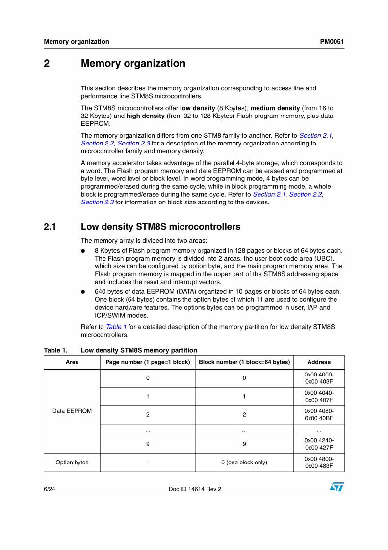
2.1 Low density STM8S microcontrollersThe memory array is divided into two areas:
● 8 Kbytes of Flash program memory organized in 128 pages or blocks of 64 bytes each. The Flash program memory is divided into 2 areas, the user boot code area (UBC), which size can be configured by option byte, and the main program memory area. The Flash program memory is mapped in the upper part of the STM8S addressing space and includes the reset and interrupt vectors.
● 640 bytes of data EEPROM (DATA) organized in 10 pages or blocks of 64 bytes each. One block (64 bytes) contains the option bytes of which 11 are used to configure the device hardware features. The options bytes can be programmed in user, IAP and ICP/SWIM modes.
Refer to Table 1 for a detailed description of the memory partition for low density STM8S microcontrollers.
Table 1. Low density STM8S memory partition
Area Page number (1 page=1 block) Block number (1 block=64 bytes) Address
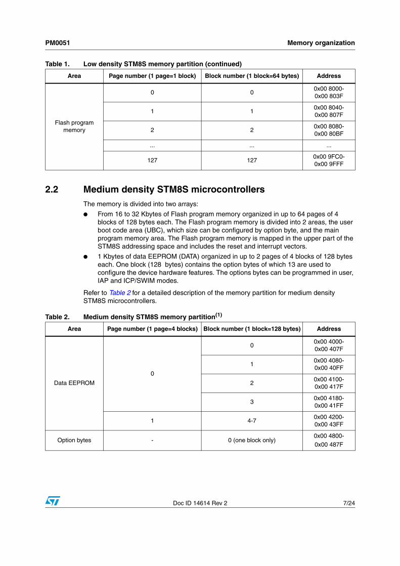
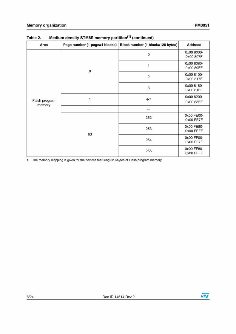
2.2 Medium density STM8S microcontrollersThe memory is divided into two arrays:
● From 16 to 32 Kbytes of Flash program memory organized in up to 64 pages of 4 blocks of 128 bytes each. The Flash program memory is divided into 2 areas, the user boot code area (UBC), which size can be configured by option byte, and the main program memory area. The Flash program memory is mapped in the upper part of the STM8S addressing space and includes the reset and interrupt vectors.
● 1 Kbytes of data EEPROM (DATA) organized in up to 2 pages of 4 blocks of 128 bytes each. One block (128 bytes) contains the option bytes of which 13 are used to configure the device hardware features. The options bytes can be programmed in user, IAP and ICP/SWIM modes.
Refer to Table 2 for a detailed description of the memory partition for medium density STM8S microcontrollers.
Flash program memory
0 00x00 8000-0x00 803F
1 10x00 8040-0x00 807F
2 20x00 8080-0x00 80BF
... ... ...
127 1270x00 9FC0-0x00 9FFF
Table 1. Low density STM8S memory partition (continued)
Area Page number (1 page=1 block) Block number (1 block=64 bytes) Address
Table 2. Medium density STM8S memory partition(1)
Area Page number (1 page=4 blocks) Block number (1 block=128 bytes) Address
1. The memory mapping is given for the devices featuring 32 Kbytes of Flash program memory.
Table 2. Medium density STM8S memory partition(1) (continued)
Area Page number (1 page=4 blocks) Block number (1 block=128 bytes) Address
PM0051 Memory organization
Doc ID 14614 Rev 2 9/24
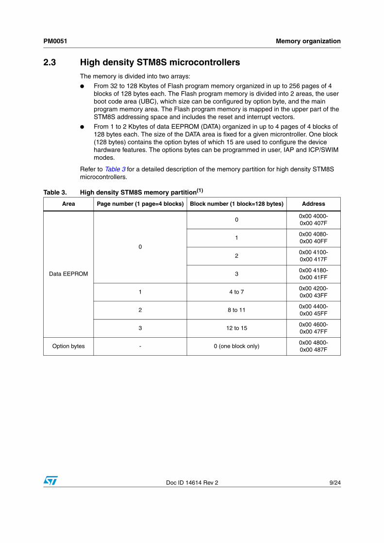
2.3 High density STM8S microcontrollersThe memory is divided into two arrays:
● From 32 to 128 Kbytes of Flash program memory organized in up to 256 pages of 4 blocks of 128 bytes each. The Flash program memory is divided into 2 areas, the user boot code area (UBC), which size can be configured by option byte, and the main program memory area. The Flash program memory is mapped in the upper part of the STM8S addressing space and includes the reset and interrupt vectors.
● From 1 to 2 Kbytes of data EEPROM (DATA) organized in up to 4 pages of 4 blocks of 128 bytes each. The size of the DATA area is fixed for a given microntroller. One block (128 bytes) contains the option bytes of which 15 are used to configure the device hardware features. The options bytes can be programmed in user, IAP and ICP/SWIM modes.
Refer to Table 3 for a detailed description of the memory partition for high density STM8S microcontrollers.
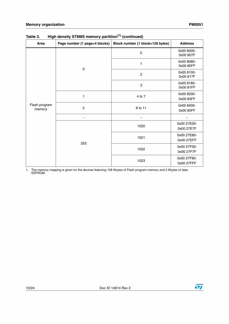
Table 3. High density STM8S memory partition(1)
Area Page number (1 page=4 blocks) Block number (1 block=128 bytes) Address
1. The memory mapping is given for the devices featuring 128 Kbytes of Flash program memory and 2 Kbytes of data EEPROM.
Table 3. High density STM8S memory partition(1) (continued)
Area Page number (1 page=4 blocks) Block number (1 block=128 bytes) Address
PM0051 Memory protection strategy
Doc ID 14614 Rev 2 11/24
3 Memory protection strategy
The STM8 devices feature several mechanisms allowing to protect the content of the Flash program and data EEPROM areas:
● Readout protection
The software can prevent application code and data stored in the Flash program memory and data EEPROM from being read and modified in ICP mode. The readout protection is enabled and disabled by programming an option byte in ICP mode. Refer to Section 3.1 for details.
● User boot code area (UBC)
In order to guaranty the capability to recover from an interrupted or erroneous IAP programming, all STM8 devices provide a write-protected area called user boot code (UBC). This area is a part of the Flash program memory which cannot be modified in user mode (that is protected against modification by the user software). The content of the UBC area can be modified only in ICP (SWIM) mode after clearing the UBC option byte.
The size of the user boot code area can be programmed through an option byte by increments of one page.
Refer to Section 3.2 for details on user boot code area.
● Unwanted memory access protection
All STM8 devices offer unwanted memory access protection, which purpose is to prevent unintentional modification of program memory and data EEPROM (for example due to a firmware bug or EMC disturbance).
This protection consists of authorizing write access to the memory only through a specific software sequence which is unlikely to happen randomly or by mistake. Access to Flash program and data EEPROM areas is enabled by writing MASS keys into key registers.
Refer to Section 3.3 for details on unwanted memory access protection.
3.1 Readout protectionThe readout protection can be set by writing 0xAA in the ROP option byte. It can be disabled by reprogramming the ROP option byte. Enabling and disabling readout protection is possible only in ICP mode.
When the readout protection is selected, reading or modifying the Flash program memory in ICP mode (using the SWIM interface) is forbidden. When available, the data EEPROM memory is also protected against read and write access through ICP.
Erasing the ROP option byte to disable the readout protection causes the Flash program memory, the DATA area and the option bytes to be erased.
Even though no protection can be considered as totally unbreakable, the readout protection feature provides a very high level of protection for general purpose microcontrollers. Of course, a software that allows the user to dump the Flash program memory content make this readout protection useless. Table 6 describes possible accesses to each memory areas versus the different modes and readout protection settings.
Memory protection strategy PM0051
12/24 Doc ID 14614 Rev 2
3.2 User Boot Code area protectionWhatever the memory content, it is always possible to restart an ICP session after a critical error by applying a reset and restarting the SWIM communication.
On the contrary, during IAP sessions, the programming software driver must always be write protected to be able to recover from any critical failure that might happen during programming (such as power failure).
The pages where the IAP driver is implemented must be located in the write-protected boot code area (UBC). The application reset and interrupt vectors and the reset routine must also be stored in the UBC. These conditions allow the user software to manage the recovery from potential critical failure by applying a reset and restarting the IAP routine from the protected boot area.
The UBC size is defined in the user boot code (UBC) area option byte. This option byte may slightly differ from one product to another. See Table 4 for the minimum size of the UBC area. Its maximum size is equal to the full memory size.
The FLASH_FPR and FLASH_NFPR registers reflect the value of the UBC and NUBC option bytes, respectively.
3.3 Unwanted memory access protectionThe unwanted memory access protection consists of writing two 8-bit keys in the right order into dedicated MASS key registers.
Writing the correct sequence of keys in the program memory MASS key register (FLASH_PUKR) enables the programming of the program memory area excluding the UBC. If wrong keys are provided, a reset must to be generated to be able to reprogram the right keys.
Once the write memory protection has been removed, it is possible to reactivate the protection of the area by resetting the PUL bit in FLASH_IAPSR.
To enable write access to the data EEPROM area, another specific MASS key register (FLASH_DUKR) and a different key sequence must be used. Once the data EEPROM/option byte area is unlocked, it is possible to reactivate the protection of the area by resetting the DUL bit in FLASH_IAPSR.
If wrong keys have been provided to the FLASH_PUKR register, the device must be reset before performing a new key program sequence. However, when wrong keys are provided to the FLASH_DUKR register, new keys can be entered without the device being previously reset.
In order to be as effective as possible, the application software must lock again the unwanted memory access protection as soon as the programming is completed. Otherwise, the protection level of the MASS is significantly reduced. To activate the MASS protection
Table 4. Minimum size of the UBC area
STM8 microcontroller family Minimum size of the UBC area
Low density STM8S 2 pages = 128 bytes
Medium density STM8S2 pages = 1 Kbytes
High density STM8S
PM0051 Programming STM8 Flash microcontrollers
Doc ID 14614 Rev 2 13/24
again, the user must reset the corresponding bits in the FLASH_IAPSR register (DUL bit for data EEPROM or PUL bit for Flash program memory).
Note: 1 The mechanism to lock and unlock unwanted memory access protection is identical for option bytes and data EEPROM (see Table 5: MASS).
2 Before starting programming program memory or data EEPROM, the software must verify that the area is not write protected by checking that the PUL or DUL bit is effectively set.
4 Programming STM8 Flash microcontrollers
This section describes how to program STM8 single-voltage Flash microcontrollers.
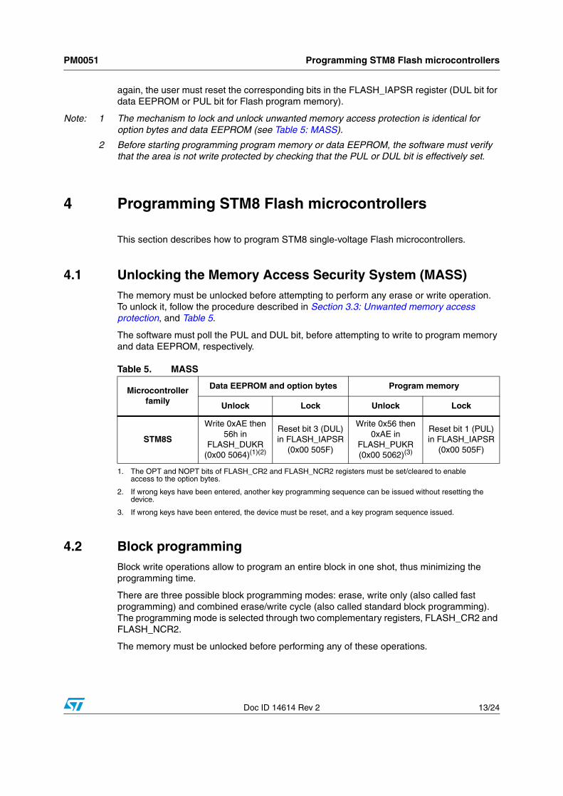
4.1 Unlocking the Memory Access Security System (MASS)The memory must be unlocked before attempting to perform any erase or write operation. To unlock it, follow the procedure described in Section 3.3: Unwanted memory access protection, and Table 5.
The software must poll the PUL and DUL bit, before attempting to write to program memory and data EEPROM, respectively.
4.2 Block programmingBlock write operations allow to program an entire block in one shot, thus minimizing the programming time.
There are three possible block programming modes: erase, write only (also called fast programming) and combined erase/write cycle (also called standard block programming). The programming mode is selected through two complementary registers, FLASH_CR2 and FLASH_NCR2.
The memory must be unlocked before performing any of these operations.
Table 5. MASS
Microcontroller family
Data EEPROM and option bytes Program memory
Unlock Lock Unlock Lock
STM8S
Write 0xAE then 56h in
FLASH_DUKR(0x00 5064)(1)(2)
1. The OPT and NOPT bits of FLASH_CR2 and FLASH_NCR2 registers must be set/cleared to enable access to the option bytes.
2. If wrong keys have been entered, another key programming sequence can be issued without resetting the device.
Reset bit 3 (DUL) in FLASH_IAPSR
(0x00 505F)
Write 0x56 then 0xAE in
FLASH_PUKR(0x00 5062)(3)
3. If wrong keys have been entered, the device must be reset, and a key program sequence issued.
Reset bit 1 (PUL) in FLASH_IAPSR
(0x00 505F)
Programming STM8 Flash microcontrollers PM0051
14/24 Doc ID 14614 Rev 2
Block program operations can be performed both to main program memory and DATA area:
● Programming a block of main program memory:
The block program operation has to be executed totally from RAM.
The program execution continues from RAM. If the program goes back to main program memory, it is stalled until the block program operation is complete.
● Programming a block of data EEPROM with RWW capability:
The block program operation can be executed from main program memory. However the data loading phase (see below) has to be executed from RAM.
Normal program execution can continue from main program memory (after checking the HVOFF bit in the FLASH_IAPSR register).
● Programming a block of data EEPROM on devices without RWW capability:
The block program operation must be executed totally from RAM.
The programming can also be performed directly through the SWIM interface. In this case, it is recommended to stall the device in order to prevent the core from accessing the Flash program memory during the block program or erase operation. This can be done by setting the STALL bit in the DM_CSR2 debug module register. Refer to the STM8 SWIM communication protocol and debug module (UM0470) for more information.
Caution: During a block program or erase operation, it is recommended to avoid executing instructions performing a read access to program memory.
Caution: If the number of written memory locations is higher than what is required in the block program/erase sequence, the additional locations are handled as redundant byte write operations.
If the number of written memory locations is lower than what is specified in the block program/erase sequence, the block program/erase process does not start and the CPU stalls waiting for the remaining operations to be performed.
Caution: EOP and WR_PG_DIS bits of FLASH_IAPSR register are automatically cleared when a program/erase operation starts.
Caution: If a block program or erase sequence is interrupted by a reset, the data programmed in the memory may be corrupted.
PM0051 Programming STM8 Flash microcontrollers
Doc ID 14614 Rev 2 15/24
Standard block programming
The following sequence is required to perform a standard block program sequence (block erased and programmed):
1. Unlock the memory if not already done.
The UBC option byte can be read to check if the block to program is not in the UBC area. If necessary, reprogram it to allow erasing and programming the targeted block.
2. Write 0x01 in FLASH_CR2 (PRG bit active), and 0xFE in FLASH_NCR2 (NPRG bit active).
3. Write all the data bytes of the block you want to program starting with the very first address of the block. No read or write access to the program memory is allowed during these load operations as they might corrupt the values to be programmed.
The programming cycle starts automatically when all the data in the block have been written.
4. Check the WR_PG_DIS bit in FLASH_IAPSR to verify if the block you attempted to program was not write protected (optional)
5. For devices with RWW capability, poll the HVOFF bit in FLASH_IAPSR register for the start of program operation (high voltage mode). HVOFF is reset when the program operation starts, thus indicating that the memory is ready for RWW.
6. Poll the EOP bit in FLASH_IAPSR from program memory. EOP is set to ‘1’ when the standard block program operation has completed. To avoid polling the EOP bit, an interrupt can generated when EOP is set.
Note: It is mandatory to execute steps 2 to 5 from RAM.
Caution: EOP and WR_PG_DIS bits are cleared by reading the FLASH_IAPSR register. It is consequently strongly recommended to perform one single read operation to the FLASH_IAPSR register to check the values of these bits.
Caution: FLASH_CR2 and FLASH_NCR2 must be written consecutively to be taken into account. If only one register is set, both are forced to their reset values, causing the program operation to be performed at byte level.
Programming STM8 Flash microcontrollers PM0051
16/24 Doc ID 14614 Rev 2
Fast block programming operation
The following sequence is required to perform a fast block program sequence (block programmed without previous erase):
1. Unlock the memory if not already done.
The UBC option byte can be read to check if the block to program is not in the UBC area. If necessary, reprogram it to allow programming the targeted block.
2. Write 0x10 in FLASH_CR2 (FPRG bit active), and 0xEF in FLASH_NCR2 (NFPRG bit active).
3. Write all the data bytes of the block you want to program starting with the very first address of the block. No read or write access to the program memory is allowed during these load operations as they might corrupt the values to be programmed.
The programming cycle starts automatically when the complete block has been written.
4. Check the WR_PG_DIS bit in FLASH_IAPSR to verify if the block you attempted to program was not write protected (optional).
5. For devices with RWW capability, poll the HVOFF bit in FLASH_IAPSR register for the start of program operation (high voltage mode). HVOFF is reset when the program operation starts, thus indicating that the memory is ready for RWW.
6. Poll the EOP bit in FLASH_IAPSR from program memory. EOP is set to ‘1’ when the block program operation has completed. To avoid polling the EOP bit, an interrupt can generated when EOP is set.
Note: It is mandatory that steps 2 to 5 are executed from RAM.
Caution: FLASH_CR2 and FLASH_NCR2 must be written consecutively to be taken into account. If only one register is set, both are forced to their reset values, causing the program operation to be performed at byte level.
Caution: EOP and WR_PG_DIS bits are cleared by reading the FLASH_IAPSR register. It is consequently strongly recommended to perform one single read operation to the FLASH_IAPSR register to check the values of these bits.
Caution: The memory block must be empty when performing a fast block programming operation.
PM0051 Programming STM8 Flash microcontrollers
Doc ID 14614 Rev 2 17/24
Block erase operation
The following sequence is required to perform a block erase sequence:
1. Unlock the memory if not already done.
The UBC option byte can be read to check if the block to erase is not in the UBC area. If necessary, reprogram it to allow erasing the targeted block.
2. Write 0x20 in FLASH_CR2 (ERASE bit active), and 0xDF in FLASH_NCR2 (NERASE bit active).
3. Write '0x00 00 00 00' to any word inside the block to be erased using a LOAD instruction.
4. Check the WR_PG_DIS bit in FLASH_IAPSR to verify if the block you attempted to erase was not write protected (optional).
5. For devices with RWW capability, poll the HVOFF bit in FLASH_IAPSR register for the start of erase operation (high voltage mode). HVOFF is reset when the erase operation starts, thus indicating that the memory is ready for RWW.
6. Poll the EOP bit in FLASH_IAPSR from program memory. EOP is set to ‘1’ when the block erase operation has completed. To avoid polling the EOP bit, an interrupt can generated when EOP is set.
Note: It is mandatory to execute steps 2 to 5 from RAM.
Caution: EOP and WR_PG_DIS bits are cleared by reading the FLASH_IAPSR register. It is consequently strongly recommended to perform one single read operation to the FLASH_IAPSR register to check the values of these bits.
Caution: FLASH_CR2 and FLASH_NCR2 must be written consecutively to be taken into account. If only one register is set, both are forced to their reset values, causing the erase operation to be performed at byte level.
4.3 Word programmingBoth main program memory and data EEPROM can be programmed and erased at word level. Word operations are performed in the same way as block operations. They can be executed either from program memory or from RAM.
When a new word program operation starts, EOP and WR_PG_DIS bits of FLASH_IAPSR register are automatically cleared.
The following sequence is required to perform a word program operation:
1. Unlock the memory if not already done.
The UBC option byte can be read to check if the word you want to program is not in the UBC area. If necessary, reprogram it to allow programming the targeted word.
2. Write 0x40 in FLASH_CR2 (WP bit active), and 0xBF in FLASH_NCR2 (NWP bit active).
3. Write the 4 data bytes to the memory starting with the very first address of the word to be programmed.
The programming cycle starts automatically when the 4 bytes have been written.
4. Check the WR_PG_DIS bit in FLASH_IAPSR to verify if the word you attempted to program was not write-protected (optional).
5. Poll the EOP bit in FLASH_IAPSR register for the end of operations. EOP is set to ‘1’ when the word program operation has completed.
Programming STM8 Flash microcontrollers PM0051
18/24 Doc ID 14614 Rev 2
Caution: FLASH_CR2 and FLASH_NCR2 must be written consecutively to be taken into account. If only one register is set, both are forced to their reset values, causing the program operation to be performed at byte level.
Caution: EOP and WR_PG_DIS bits are cleared by reading the FLASH_IAPSR register. It is consequently strongly recommended to perform one single read operation to the FLASH_IAPSR register to check the values of these bits.
Caution: If a word program operation is interrupted by a reset, the data programmed in the memory may be corrupted.
4.4 Byte programmingBoth main program memory and data EEPROM can be programmed and erased at byte level.
Byte programming is performed by executing a write instruction (ld, mov...) to an address in main program memory when the memory is unlocked. The write instruction initiates the erase/program cycle and any core access to the memory is blocked until the cycle has completed. This means that program execution from the Flash program memory is stopped until the end of the erase/program cycle.
When a new word program operation starts, EOP and WR_PG_DIS bits of FLASH_IAPSR register are automatically cleared. At the end of the program operation, the EOP bit in the FLASH_IAPSR register is set and the program execution restarts from the instruction following the write/erase instruction.
Contrary to byte programming of the Flash program memory, the byte programming of data EEPROM with RWW feature (when available) does not stop program execution. The EOP bit can then be used in order to know if the previous operation has completed. This bit is automatically reset when reading FLASH_IAPSR.
The erase/program cycle lasts longer if the whole word containing the byte to be programmed is not empty because in this case an erase operation is performed automatically. If the word is empty, the erase operation is not performed. However, if a defined programming time is wanted, the FIX bit in the FLASH_CR1 register forces the programming operation to always erase first whatever the contents of the memory. Therefore a fixed programming time is guaranteed (erase time + write time).
To erase a byte location, just write ‘0x00’ to the byte location.
Caution: If a byte program operation is interrupted by a reset, the data programmed in the memory may be corrupted.
4.5 Programming the option bytesOption bytes are used to configure the device hardware features as well as the memory protection. They are stored in a dedicated memory block.
PM0051 Programming STM8 Flash microcontrollers
Doc ID 14614 Rev 2 19/24
4.5.1 Summary of memory dedicated option bytes
The Flash program memory includes several option bytes dedicated to memory protection:
● ROP
The ROP option byte is used to prevent the Flash program memory from being read and modified in ICP mode. Refer to Section 3.1: Readout protection for a detailed description of readout protection.
● UBC
The UBC option byte is used to program the size of the write protected user boot code area. The boot area always includes the reset and interrupt vectors and can go up to the full program memory size. The boot area size granularity is of one page.
Refer to Section 3.2: User Boot Code area protection for a detailed description of the UBC area.
4.5.2 How to program the option bytes
To enhance security on STM8S devices, option bytes must be programmed twice, once in a regular form and once in a complemented form. If both values are not complementary, the default value is forced, ensuring a safe configuration.
Option bytes can be modified both in user/IAP mode and ICP mode (using the SWIM), except for the readout protection which can only be removed in ICP mode. In ICP mode, the OPT and NOPT bits of the FLASH_CR2 and FLASH_NCR2 registers must be set to their active state before attempting to modify the option bytes (OPT = 1 and NOPT = 0).
Programming STM8 Flash microcontrollers PM0051
20/24 Doc ID 14614 Rev 2
4.6 Memory access versus programming methodTable 6 gives a description of possible accesses from the core to memory areas according to the programming method.
Table 6. Memory access versus programming method(1)
Mode ROP Memory AreaSTM8S
Access from core
User, IAP, and Bootloader (if available)
Readout protection enabled
Interrupt vectors R/W(2)/E
User boot code area (UBC) R/E
Main program R/W/E(3)
Data EEPROM area (DATA) R/W(4)
Option bytes R
Readout protection disabled
Interrupt vectors R/W(2)/E
User boot code area (UBC) R/E(5)
Main program R/W/E(3)
Data EEPROM area (DATA) R/W(4)
Option bytes R/W(6)
SWIM active (ICP mode)
Readout protection enabled
Interrupt vectors P
User boot code area (UBC) P
Main program P
Data EEPROM area (DATA) P
Option bytes P/WROP(7)
Readout protection disabled
Interrupt vectors R/W(2)/E
User boot code area (UBC) R/E(5)
Main program R/W/E(3)
Data EEPROM area (DATA) R/W(4)
Option bytes R/W(6)
1. R/W/E = Read; Write and Execute; R/E = Read and Execute (write operation forbidden); R = Read (write and execute operations forbidden); P = the area cannot be accessed (read, execute and write operations forbidden);P/WROP = Protected, write forbidden except for ROP option byte.
2. When no UBC area has been defined, the interrupt vectors can be modified in user /IAP mode.
3. The Flash program memory is write protected (locked) until the correct MASS key is written in the FLASH_PUKR. It is possible to lock the memory again by resetting the PUL bit in the FLASH_IAPSR register. If wrong keys are provided, the device must be reset and new keys programmed.
4. The data memory is write protected (locked) until the correct MASS key is written in the FLASH_DUKR. It is possible to lock the memory again by resetting the DUL bit in the FLASH_IAPSR register. If wrong keys are provided, another key program sequence can be performed without resetting the device.
5. To program the UBC area the application must first clear the UBC option byte.
6. The option bytes are write protected (locked) until the correct MASS key is written in the FLASH_DUKR (with OPT set to ‘1’). It is possible to lock the memory again by resetting the DUL bit in the IAPSR register. If wrong keys are provided, another key program sequence can be performed without resetting the device.
7. When ROP is removed, the whole memory is erased, including the option bytes.
PM0051 Programming STM8 Flash microcontrollers
Doc ID 14614 Rev 2 21/24
4.6.1 ICP methods
The in-circuit programming (ICP) method is used to update the content of Flash program memory and data EEPROM.
The programming interface for STM8 devices is the SWIM (Single Wire Interface Module). It is used to communicate with an external programming device connected via a cable.
See STM8 SWIM communication protocol and debug module user manual (UM0470) for more details on the SWIM mode entry and SWIM protocol.
When using the SWIM protocol, two methods can be used:
First method
The first method consists of writing directly into the Flash registers and memory locations through the write memory command of the SWIM protocol. To make sure that the CPU is not accessing the memory during block Flash programming, the core must be stalled by setting the STALL bit in the DM_CSR2 debug module register.
The following sequence is required:
1. Apply a RESET
2. Activate the SWIM by sending the entry sequence on the SWIM pin
3. Activate the SWIM_CSR register by writing 1 to the DM bit in SWIM_CSR
4. Disable interrupts by setting the SAFE_MASK bit in SWIM_CSR
5. Release RESET
6. Verify the DeviceID by reading it using ROTF command
7. Send the SWIM SRST command
8. Unlock the memory by writing the MASS keys
9. Program the Flash program memory using the SWIM WOTF command
Second method
The second method uses the same sequence of operations as the first method except that the ICP driver firmware must be downloaded in RAM before being launched:
1. Apply a RESET
2. Activate the SWIM by sending the entry sequence on the SWIM pin
3. Activate the SWIM_CSR register by writing 1 to the DM bit in SWIM_CSR
4. Disable interrupts by setting the SAFE_MASK bit in SWIM_CSR
5. Release RESET
6. Verify the DeviceID by reading it using ROTF command
7. Send the SWIM SRST command
8. Unlock the memory by writing the MASS keys
9. Download the ICP driver firmware into the device RAM using the SWIM WOTF command
10. Execute the ICP driver:
a) Modify the CPU registers (new PC, X, Y, CC...) using the WOTF commands
b) Set the FLASH bit in the DM_CSR2 register
c) Clear the STALL bit in the DM_CSR2 register
Flash program memory and data EEPROM comparison PM0051
22/24 Doc ID 14614 Rev 2
4.6.2 IAP method
Refer to application note AN2737- Basic in-application programming example using the
STM8 I2C and SPI peripherals.
5 Flash program memory and data EEPROM comparison
Table 7 shows the comparison between STM8S microcontroller devices.
Table 7. Comparison between STM8S devices
Feature Low density STM8S Medium density STM8S High density STM8S
Flash program memory Up to 8 Kbytes From 16 to 32 Kbytes From 32 to 128 Kbytes
Data EEPROM
Additional 640 bytes located in the same memory array as
Flash programFixed size
1 Kbytes located in separate memory array
Fixed size
Up to 2 Kbytes located in separate memory array
Fixed size
User boot code (UBC) YES - size configurable by option byte
Bootloader NO YES
Option bytes
Programmable in ICP/SWIM, IAP
Stored twice (normal+complemented
value)
2 memory dedicated option bytes (ROP, UBC)
Programmable in ICP/SWIM,IAP/ Bootloader
Stored twice (normal+complemented value)
2 memory dedicated option bytes (ROP, UBC)
Programming/erasing features
Read-while-write (RWW) NO(1) YES
Block programming (fast and standard)(2)
Word programming(2)
Byte programming(2)
Block Erase(2)(3)
YES
Flash control registers FLASH_NCR2, FLASH_CR2 containing complementary values
1. The read-while-write (RWW) feature is not available on the 4-8 Kbyte STM8S because data EEPROM and Flash program memory are located in the same memory array.
2. Block program/erase sequence must be executed from RAM.
3. Any word in the block programmed to 0.
PM0051 Revision history
Doc ID 14614 Rev 2 23/24
6 Revision history
Table 8. Document revision history
Date Revision Changes
16-Feb-2009 1 Initial release.
12-Jun-2009 2
Added caution note related to FLASH_IAPSR register in Section 4.2: Block programming and Section 4.3: Word programmingUpdated Section 4.2: Block programming.
Updated memory access table (Table 6) (STM8S):
– Access from core specified
PM0051
24/24 Doc ID 14614 Rev 2
Please Read Carefully:
Information in this document is provided solely in connection with ST products. STMicroelectronics NV and its subsidiaries (“ST”) reserve theright to make changes, corrections, modifications or improvements, to this document, and the products and services described herein at anytime, without notice.
All ST products are sold pursuant to ST’s terms and conditions of sale.
Purchasers are solely responsible for the choice, selection and use of the ST products and services described herein, and ST assumes noliability whatsoever relating to the choice, selection or use of the ST products and services described herein.
No license, express or implied, by estoppel or otherwise, to any intellectual property rights is granted under this document. If any part of thisdocument refers to any third party products or services it shall not be deemed a license grant by ST for the use of such third party productsor services, or any intellectual property contained therein or considered as a warranty covering the use in any manner whatsoever of suchthird party products or services or any intellectual property contained therein.
UNLESS OTHERWISE SET FORTH IN ST’S TERMS AND CONDITIONS OF SALE ST DISCLAIMS ANY EXPRESS OR IMPLIEDWARRANTY WITH RESPECT TO THE USE AND/OR SALE OF ST PRODUCTS INCLUDING WITHOUT LIMITATION IMPLIEDWARRANTIES OF MERCHANTABILITY, FITNESS FOR A PARTICULAR PURPOSE (AND THEIR EQUIVALENTS UNDER THE LAWSOF ANY JURISDICTION), OR INFRINGEMENT OF ANY PATENT, COPYRIGHT OR OTHER INTELLECTUAL PROPERTY RIGHT.
UNLESS EXPRESSLY APPROVED IN WRITING BY AN AUTHORIZED ST REPRESENTATIVE, ST PRODUCTS ARE NOTRECOMMENDED, AUTHORIZED OR WARRANTED FOR USE IN MILITARY, AIR CRAFT, SPACE, LIFE SAVING, OR LIFE SUSTAININGAPPLICATIONS, NOR IN PRODUCTS OR SYSTEMS WHERE FAILURE OR MALFUNCTION MAY RESULT IN PERSONAL INJURY,DEATH, OR SEVERE PROPERTY OR ENVIRONMENTAL DAMAGE. ST PRODUCTS WHICH ARE NOT SPECIFIED AS "AUTOMOTIVEGRADE" MAY ONLY BE USED IN AUTOMOTIVE APPLICATIONS AT USER’S OWN RISK.
Resale of ST products with provisions different from the statements and/or technical features set forth in this document shall immediately voidany warranty granted by ST for the ST product or service described herein and shall not create or extend in any manner whatsoever, anyliability of ST.
ST and the ST logo are trademarks or registered trademarks of ST in various countries.
Information in this document supersedes and replaces all information previously supplied.
The ST logo is a registered trademark of STMicroelectronics. All other names are the property of their respective owners.
Australia - Belgium - Brazil - Canada - China - Czech Republic - Finland - France - Germany - Hong Kong - India - Israel - Italy - Japan - Malaysia - Malta - Morocco - Philippines - Singapore - Spain - Sweden - Switzerland - United Kingdom - United States of America