Broadcom Proprietary. Not for distribution outside the company - 1 - Description Broadcom Power PLCC-4 is an extension of our PLCC2 SMT LEDs. The package can be driven at higher current due to its superior package design. The product is able to dissipate heat more efficiently compared to the conventional PLCC-2 SMT LEDs. In proportion to the increase in driving current, this family of LEDs is able to produce higher light output compared to the conventional PLCC-2 SMT LEDs. These SMT LEDs have higher reliability and better performance and are designed to work under a wide range of environmental conditions. This higher reliability makes them suitable for use under harsh environment and conditions like automotive. In addition, they are also suitable to be used in electronic signs and signals. To facilitate easy pick and place assembly, the LEDs are packed in EIA-compliant tape and reel. Every reel will be shipped in single intensity and color bin (except for red color), to provide close uniformity. These LEDs are compatible with IR solder reflow process. Due to the high reliability feature of these products, they also can be mounted using through-the-wave soldering process. There are a variety of colors and various viewing angles (30°, 60°, and 120°) available in these SMT LEDs. Ideally, the 30° parts are suitable for light piping where focused intensities are required. As for the 60° and 120°, they are most suitable for automotive interior and exterior lighting and electronic signs applications. Features Industry standard PLCC-4 High reliability LED package High brightness using AlInGaP and InGaN dice technologies High optical efficiency Higher ambient temperature at the same current possible compared to PLCC-2 Available in full selection of colors Super wide viewing angle at 120° Available in 8mm carrier tape on 7-inch reel Compatible with both IR and TTW soldering process JEDEC MSL 2a High reliability LED package due to enhanced silicone resin material for InGaN family Applications Interior automotive — Instrument panel backlighting — Central console backlighting — Cabin backlighting — Navigation and audio system — Dome lighting — Push button backlighting Exterior automotive — Turn signals — CHMSL — Rear combination lamp — Puddle light Electronic signs and signals — Interior full color sign — Variable message sign Office automation, home appliances, industrial equipment — Front panel backlighting — Push button backlighting — Display backlighting HSMx-A4xx-xxxxx SMT LED Surface Mount LED Indicator Data Sheet
Transcript
Broadcom Proprietary. Not for distribution outside the company- 1 -
DescriptionBroadcom Power PLCC-4 is an extension of our PLCC2 SMT LEDs. The package can be driven at higher current due to its superior package design. The product is able to dissipate heat more efficiently compared to the conventional PLCC-2 SMT LEDs. In proportion to the increase in driving current, this family of LEDs is able to produce higher light output compared to the conventional PLCC-2 SMT LEDs.
These SMT LEDs have higher reliability and better performance and are designed to work under a wide range of environmental conditions. This higher reliability makes them suitable for use under harsh environment and conditions like automotive. In addition, they are also suitable to be used in electronic signs and signals.
To facilitate easy pick and place assembly, the LEDs are packed in EIA-compliant tape and reel. Every reel will be shipped in single intensity and color bin (except for red color), to provide close uniformity.
These LEDs are compatible with IR solder reflow process. Due to the high reliability feature of these products, they also can be mounted using through-the-wave soldering process.
There are a variety of colors and various viewing angles (30°, 60°, and 120°) available in these SMT LEDs. Ideally, the 30° parts are suitable for light piping where focused intensities are required. As for the 60° and 120°, they are most suitable for automotive interior and exterior lighting and electronic signs applications.
Features Industry standard PLCC-4 High reliability LED package High brightness using AlInGaP and InGaN dice
technologies
High optical efficiency Higher ambient temperature at the same current possible
compared to PLCC-2 Available in full selection of colors Super wide viewing angle at 120° Available in 8mm carrier tape on 7-inch reel Compatible with both IR and TTW soldering process JEDEC MSL 2a High reliability LED package due to enhanced silicone
resin material for InGaN family
Applications
Interior automotive— Instrument panel backlighting— Central console backlighting— Cabin backlighting— Navigation and audio system— Dome lighting— Push button backlighting
Electronic signs and signals— Interior full color sign— Variable message sign
Office automation, home appliances, industrial equipment— Front panel backlighting— Push button backlighting— Display backlighting
HSMx-A4xx-xxxxxSMT LED Surface Mount LED Indicator
Data Sheet
Broadcom- 2 -
HSMx-A4xx-xxxxxData Sheet
Device Selection Guide
Figure 1 Package Dimensions
NOTE All dimensions in millimeters. Electrical connection between all cathodes is recommended.
Device Selection Guide
Color Part Number Min. IV (mcd)a
a. The luminous intensity IV, is measured at the mechanical axis of the lamp package. The actual peak of the spatial radiation pattern may not be aligned with this axis. IV tolerance = ±12%.
Max. IV (mcd) Test Current (mA) Dice Technology
Red HSMC-A400-S30M1 180.00 355.00 50 AlInGaP
HSMC-A401-U80M1 560.00 1400.00 50 AlInGaP
Red Orange HSMJ-A401-T40M1 285.00 715.00 50 AlInGaP
HSMJ-A401-U40M1 450.00 1125.00 50 AlInGaP
Orange HSML-A401-U40M1 450.00 1125.00 50 AlInGaP
Amber HSMA-A401-U45M1 450.00 1125.00 50 AlInGaP
Emerald Green HSME-A401-P4PM1 45.00 112.50 50 AlInGaP
Blue HSMN-A400-S8QM2 224.00 560.00 30 InGaN
HSMN-A400-S8PM2 224.00 560.00 30 InGaN
HSMN-A400-S4QM2 180.00 450.00 30 InGaN
Green HSMM-A400-W8QM2 1400.00 3550.00 30 InGaN
HSMM-A400-W8YM2 1400.00 3550.00 30 InGaN
0.8 0.3
3.5 0.2
2.8 ± 0.2
0.5 ± 0.1
3.2 0.2
2.2 ± 0.2
1.9 ± 0.2
0.1 TYP. 0.8 ± 0.1
CATHODE MARKING
0.7 0.1
C C
A C
Broadcom- 3 -
HSMx-A4xx-xxxxxData Sheet
Part Numbering System
Part Numbering System
Absolute Maximum Ratings (TA = 25°C)
Parameters HSMC/J/L/A/E HSMZ/V/U HSMM/N
DC Forward Currenta
a. Derate linearly as shown in figure 5.
70 mAb c
b. Drive current between 10 mA and 70 mA is recommended for best long-term performance.
c. Operation at currents below 5 mA is not recommended.
70 mAb c 30 mA
Peak Forward Currentd
d. Duty factor = 10%, Frequency = 1 kHz.
200 mA 200 mA 90 mA
Power Dissipation 180 mW 240 mW 114 mW
Reverse Voltage — 5V —
Junction Temperature — 110°C —
Operating Temperature — –40°C to +100°C —
Storage Temperature — –40°C to +100°C —
HSM x1 – A x2 x3x4 – x5x6 x7 x8x9
Packaging Option
Color Bin Selection
Intensity Bin Select
Device Specific Configuration
Package Type
LED Chip Color
Broadcom- 4 -
HSMx-A4xx-xxxxxData Sheet
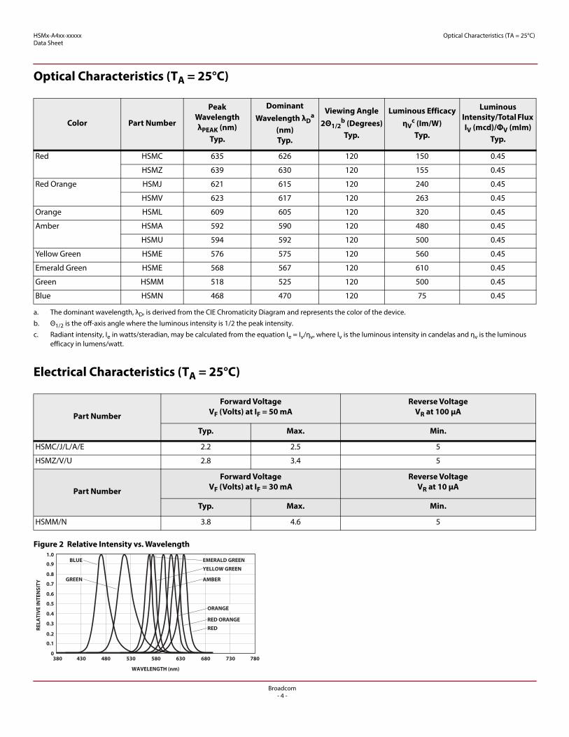
Optical Characteristics (TA = 25°C)
Optical Characteristics (TA = 25°C)
Electrical Characteristics (TA = 25°C)
Figure 2 Relative Intensity vs. Wavelength
Color Part Number
Peak Wavelength λPEAK (nm)
Typ.
Dominant Wavelength λD
a (nm)Typ.
a. The dominant wavelength, λD, is derived from the CIE Chromaticity Diagram and represents the color of the device.
Viewing Angle 2Θ1/2
b (Degrees)Typ.
b. Θ1/2 is the off-axis angle where the luminous intensity is 1/2 the peak intensity.
Luminous Efficacy ηV
c (Im/W)Typ.
c. Radiant intensity, Ie in watts/steradian, may be calculated from the equation Ie = Iv/ηv, where Iv is the luminous intensity in candelas and ηv is the luminous efficacy in lumens/watt.
Luminous Intensity/Total Flux IV (mcd)/ΦV (mIm)
Typ.
Red HSMC 635 626 120 150 0.45
HSMZ 639 630 120 155 0.45
Red Orange HSMJ 621 615 120 240 0.45
HSMV 623 617 120 263 0.45
Orange HSML 609 605 120 320 0.45
Amber HSMA 592 590 120 480 0.45
HSMU 594 592 120 500 0.45
Yellow Green HSME 576 575 120 560 0.45
Emerald Green HSME 568 567 120 610 0.45
Green HSMM 518 525 120 500 0.45
Blue HSMN 468 470 120 75 0.45
Part Number
Forward VoltageVF (Volts) at IF = 50 mA
Reverse VoltageVR at 100 μA
Typ. Max. Min.
HSMC/J/L/A/E 2.2 2.5 5
HSMZ/V/U 2.8 3.4 5
Part Number
Forward VoltageVF (Volts) at IF = 30 mA
Reverse VoltageVR at 10 μA
Typ. Max. Min.
HSMM/N 3.8 4.6 5
WAVELENGTH (nm)
EMERALD GREEN
RELA
TIV
E IN
TEN
SITY
1.0
0.8
0380 480 580 680 730 780630530430
BLUE
0.6
0.4
0.2
GREEN
YELLOW GREEN
AMBER
ORANGE
RED ORANGE
RED
0.1
0.3
0.5
0.7
0.9
Broadcom- 5 -
HSMx-A4xx-xxxxxData Sheet
Electrical Characteristics (TA = 25°C)
Figure 3 Forward Current vs. Forward Voltage Figure 4 Relative Intensity vs. Forward Current (AlInGaP)
0 3
FORWARD VOLTAGE (V)
0
20
70
80
FO
RWA
RD C
URR
ENT
(mA
)
10
50
40
60
1 2 4 5
HSMM/N
HSMZ/V/UHSMC/J/L/A/E
30
0 40
FORWARD CURRENT (mA)
0
0.4
REL
ATI
VE
INTE
NSI
TY(N
ORM
ALI
ZED
AT
50 m
A)
80
0.8
0.2
1.0
20
0.6
1.2
6010 30 70
1.4
50
Figure 5 Relative Intensity vs. Forward Current (InGaN) Figure 6 Maximum Forward Current vs. Ambient Temperature, Derated Based on TJmax = 110°C (AlInGaP)
0 20
FORWARD CURRENT (mA)
0
0.4
REL
ATI
VE
LUM
INO
US
INTE
NSI
TY(N
ORM
ALI
ZED
AT
30 m
A)
35
0.8
0.2
1.0
10
0.6
1.2
305 15 25 0
80
020 60 80 120
MA
XIM
UM
FO
RWA
RD C
URR
ENT
(mA
)
AMBIENT TEMPERATURE (˚C)
40
40
60
30
300˚C/W
20
70
100
10
350˚C/W
470˚C/W
50
Figure 7 Maximum Forward Current vs. Ambient Temperature, Derated Based on TJmax = 110°C (InGaN)
Figure 8 Dominant Wavelength vs. Forward Current – InGaN Devices
00
20 60 80 120
MA
XIM
UM
FO
RWA
RD C
URR
ENT
(mA
)
AMBIENT TEMPERATURE (˚C)
40
20
30
15
300˚C/W
10
35
100
5
350˚C/W
470˚C/W
25
0 20
CURRENT (mA)
460
480
540
DO
MIN
AN
T W
AV
ELEN
GTH
(nm
)
35
500
470
510
10
490
520
25
InGaN GREEN
5 15 30
530
InGaN BLUE
Broadcom- 6 -
HSMx-A4xx-xxxxxData Sheet
Electrical Characteristics (TA = 25°C)
Figure 9 Radiation Pattern
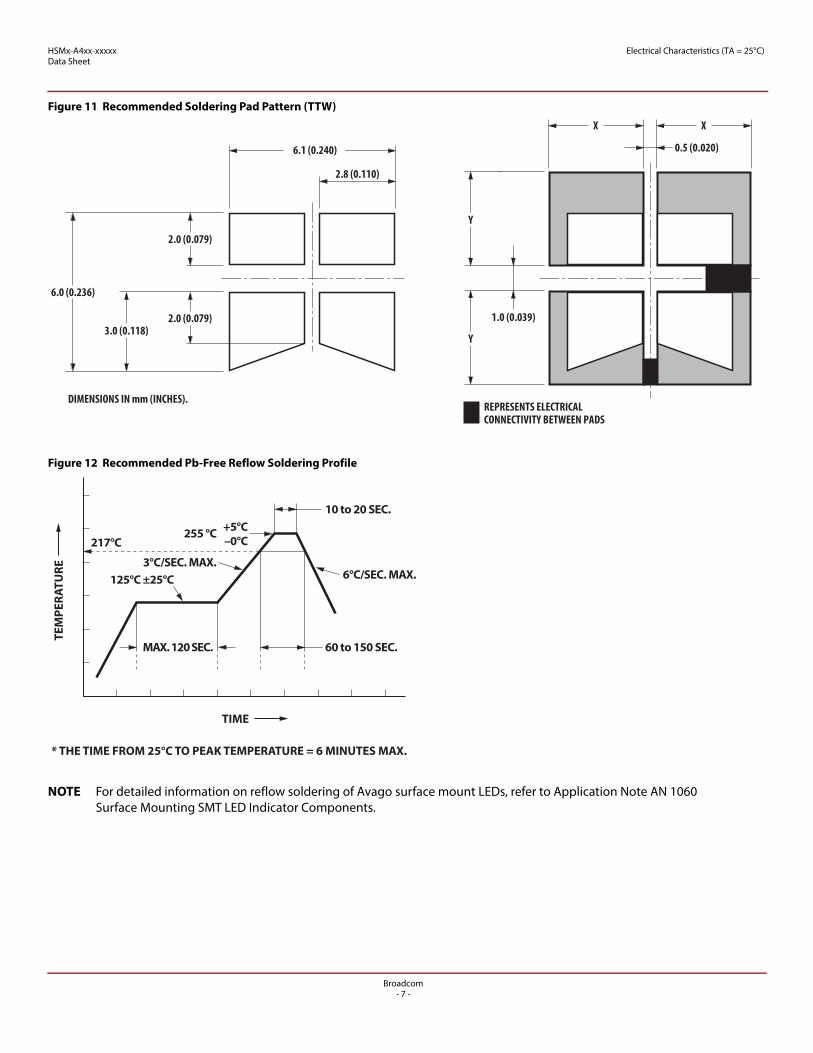
Figure 10 Recommended Soldering Pad Pattern
RELA
TIV
E IN
TEN
SITY
1.0
0
ANGLE (DEGREES)
0.8
0.6
0.2
0.4
–70 –50 –30 30 50 70 90–90 –10 10
0.1
0.3
0.5
0.7
0.9
2.60(0.103)
SOLDER RESIST REPRESENTS ELECTRICALCONNECTIVITY BETWEEN PADS
NOTE For detailed information on reflow soldering of Avago surface mount LEDs, refer to Application Note AN 1060 Surface Mounting SMT LED Indicator Components.
X X
0.5 (0.020)
Y
Y
1.0 (0.039)
2.0 (0.079)
2.0 (0.079)
6.0 (0.236)
3.0 (0.118)
2.8 (0.110)
6.1 (0.240)
DIMENSIONS IN mm (INCHES).REPRESENTS ELECTRICALCONNECTIVITY BETWEEN PADS
217°C
MAX. 120 SEC.
6°C/SEC. MAX.3°C/SEC. MAX.
125°C ±25°C
255 °C
60 to 150 SEC.
10 to 20 SEC.
TIME
TEM
PERA
TURE
* THE TIME FROM 25°C TO PEAK TEMPERATURE = 6 MINUTES MAX.
200 mm MIN. FOR Ø180 REEL.200 mm MIN. FOR Ø330 REEL.
TRAILER COMPONENT LEADER
480 mm MIN. FOR Ø180 REEL.960 mm MIN. FOR Ø330 REEL.
C
A
USER FEED DIRECTION
C
A
4 ±0.1 2 ±0.05
8 ±0.1
5.5 ±0.05
12+0.3–0.1
1.75 ±0.1
3.8 ±0.1
3.6 ±0.1
0.229 ±0.01
Ø1.5+0.1–0
Ø1+0.1–0
C
C
3.45 ±0.1
AA
VIEW A-A
VIEW B-B
B
B
ALL DIMENSIONS IN mm.
CATHODE SIDE
PRINTED LABEL
USER FEED DIRECTION
Broadcom- 9 -
HSMx-A4xx-xxxxxData Sheet
Bin Information
Bin Information
Intensity Bin Select (X5X6)
Individual reel will contain parts from one half bin only.
Intensity Bin Limits
X5 Min. IV Bin
X6
0 Full Distribution
2 2 half bins starting from X51
3 3 half bins starting from X51
4 4 half bins starting from X51
5 5 half bins starting from X51
6 2 half bins starting from X52
7 3 half bins starting from X52
8 4 half bins starting from X52
9 5 half bins starting from X52
Bin ID Min. (mcd) Max. (mcd)
N1 28.50 35.50
N2 35.50 45.00
P1 45.00 56.00
P2 56.00 71.50
Q1 71.50 90.00
Q2 90.00 112.50
R1 112.50 140.00
R2 140.00 180.00
S1 180.00 224.00
S2 224.00 285.00
T1 285.00 355.00
T2 355.00 450.00
U1 450.00 560.00
U2 560.00 715.00
V1 715.00 900.00
V2 900.00 1125.00
W1 1125.00 1400.00
W2 1400.00 1800.00
X1 1800.00 2240.00
X2 2240.00 2850.00
Y1 2850.00 3550.00
Y2 3550.00 4500.00
Z1 4500.00 5600.00
Z2 5600.00 7150.00
11 7150.00 9000.00
12 9000.00 11250.00
Broadcom- 10 -
HSMx-A4xx-xxxxxData Sheet
Bin Information
Color Bin Select (X7)
Individual reel will contain parts from one half bin only.
Color Bin Limits
NOTE Tolerance of each bin limit = ±1 nm.
X7
0 Full Distribution
Z A and B only
Y B and C only
W C and D only
V D and E only
U E and F only
T F and G only
S G and H only
Q A, B, and C only
P B, C, and D only
N C, D, and E only
M D, E, and F only
L E, F, and G only
K F, G, and H, only
1 A, B, C, and D only
2 E, F, G, and H only
3 B, C, D, and E only
4 C, D, E, and F only
5 A, B, C, D, and E only
6 B, C, D, E, and F only
Blue Min. (nm) Max. (nm)
A 460.0 465.0
B 465.0 470.0
C 470.0 475.0
D 475.0 480.0
Green Min. (nm) Max. (nm)
A 515.0 520.0
B 520.0 525.0
C 525.0 530.0
D 530.0 535.0
Emerald Green Min. (nm) Max. (nm)
A 552.5 555.5
B 555.5 558.5
C 558.5 561.5
D 561.5 564.5
Yellow Green Min. (nm) Max. (nm)
A 564.5 567.5
B 567.5 570.5
C 570.5 573.5
D 573.5 576.5
Amber/Yellow Min. (nm) Max. (nm)
A 582.0 584.5
B 584.5 587.0
C 587.0 589.5
D 589.5 592.0
E 592.0 594.5
F 594.5 597.0
Orange Min. (nm) Max. (nm)
A 597.0 600.0
B 600.0 603.0
C 603.0 606.0
D 606.0 609.0
E 609.0 612.0
Red Orange Min. (nm) Max. (nm)
A 611.0 616.0
B 616.0 620.0
Red Min. (nm) Max. (nm)
Full Distribution
Broadcom- 11 -
HSMx-A4xx-xxxxxData Sheet
Forward Voltage Bin Table
Forward Voltage Bin TableFor HSMZ/V/U – A4xx-xxxxx only.
Precautionary Notes
Handling Precautions
The encapsulation material of the LED is made of silicone for better product reliability. Compared to epoxy encapsulant that is hard and brittle, silicone is softer and flexible. Special handling precautions need to be observed during assembly of silicone encapsulated LED products. Failure to comply might lead to damage and premature failure of the LED. Refer to Application Note AN5288, Silicone Encapsulation for LED: Advantages and Handling Precautions for additional information.
1. Do not poke sharp objects into the silicone encapsulant. Sharp object like tweezers or syringes might apply excessive force or even pierce through the silicone and induce failures to the LED die or wire bond.
2. Do not touch the silicone encapsulant. Uncontrolled force acting on the silicone encapsulant might result in excessive stress on the wire bond. The LED should only be held by the body.
3. Do no stack assembled PCBs together. Use an appropriate rack to hold the PCBs.
4. Surface of silicone material attracts dusk and dirt easier than epoxy due to its surface tackiness. To remove foreign particles on the surface of silicone, a cotton bud can be used with isopropyl alcohol (IPA). During cleaning, rub the surface gently without putting much pressure on the silicone. Ultrasonic cleaning is not recommended.
5. For automated pick and place, Broadcom has tested nozzle size below to be working fine with this LED. However, due to the possibility of variations in other parameters such as pick and place machine maker/model and other settings of the machine, customer is recommended to verify the nozzle selected will not cause damage to the LED.
Handling of Moisture Sensitive Device
This product has a Moisture Sensitive Level 2arating per JEDEC J-STD-020. Refer to Application Note AN5305, Handling of Moisture Sensitive Surface Mount Devices, for additional details and a review of proper handling procedures.
1. Before use
An unopened moisture barrier bag (MBB) can be stored at <40°C/90%RH for 12 months. If the actual shelf life has exceeded 12 months and the humidity Indicator Card (HIC) indicates that baking is not required, then it is safe to reflow the LEDs per the original MSL rating.
It is recommended that the MBB not be opened prior to assembly (IQC for example).
2. Control after opening the MBB
The humidity indicator card (HIC) shall be read immediately upon opening of MBB.
The LEDs must be kept at <30°C/60%RH at all times and all high temperature related processes including soldering, curing or rework need to be completed within 672 hours.
3. Control for unfinished reel
Unused LEDs must be stored in a sealed MBB with desiccant or desiccator at <5%RH.
4. Control of assembled boards
If the PCB soldered with the LEDs is to be subjected to other high temperature processes, the PCB need to be stored in sealed MBB with desiccant or desiccator at <5%RH to ensure that all LEDs have not exceeded their floor life of 672 hours.
5. Baking is required if:
The HIC indicator is not BROWN at 10% and is AZURE at 5%.
The LEDs are exposed to condition of >30°C/60% RH at any time.
The LED floor life exceeded 168hrs. The recommended baking condition is: 60±5ºC for 20hrs.
Baking should only be done once.
Bin Min. Max.
VA 1.9 2.2
VB 2.2 2.5
VC 2.5 2.8
VD 2.8 3.1
VE 3.1 3.4
IDOD
ID = 1.7 mmOD = 3.5 mm
Broadcom- 12 -
HSMx-A4xx-xxxxxData Sheet
Precautionary Notes
6. Storage
The soldering terminals of these Broadcom LEDs are silver plated. If the LEDs are being exposed in ambient environment for too long, the silver plating might be oxidized and thus affecting its solderability performance. As such, unused LEDs must be kept in sealed MBB with desiccant or in desiccator at <5%RH.
Application Precautions
1. Drive current of the LED must not exceed the maximum allowable limit across temperature as stated in the data sheet. Constant current driving is recommended to ensure consistent performance.
2. LEDs do exhibit slightly different characteristics at different drive current which might result in larger variation their performance (meaning intensity, wavelength, and forward voltage). User is recommended to set the application current as close as possible to the test current in order to minimize these variations.
3. LED is not intended for reverse bias. Do use other appropriate components for such purpose. When driving the LED in matrix form, it is crucial to ensure that the reverse bias voltage is not exceeding the allowable limit of the LED.
4. Do not use the LED in the vicinity of material with sulfur content, in environment of high gaseous sulfur compound and corrosive elements. Examples of material that may contain sulfur are rubber gasket, RTV (room temperature vulcanizing) silicone rubber, rubber gloves etc. Prolonged exposure to such environment may affect the optical characteristics and product life.
5. Avoid rapid change in ambient temperature especially in high humidity environment as this will cause condensation on the LED.
6. Although the LED is rated as IPx6 according toIEC60529: Degree of protection provided by enclosure, the test condition may not represent actual exposure during application. If the LED is intended to be used in outdoor or harsh environment, the LED must be protected against damages caused by rain water, dust, oil, corrosive gases, external mechanical stress etc.
Thermal Management
Optical, electrical and reliability characteristics of LED are affected by temperature. The junction temperature (TJ) of the LED must be kept below allowable limit at all times. TJ can be calculated as below:
TJ = TA + RθJ-A x IF x VFmax
where;
TA = ambient temperature [°C]
RqJ-A = thermal resistance from LED junction to ambient [°C/W]
IF = forward current [A]
VFmax = maximum forward voltage [V]
The complication of using this formula lies in TA and RθJ-A. Actual TA is sometimes subjective and hard to determine. RθJ-A varies from system to system depending on design and is usually not known.
Another way of calculating TJ is by using solder point temperature TS as shown below:
TJ = TS + RθJ-S x IF x VFmax
where;
TS = LED solder point temperature as shown in illustration below [°C]
RθJ-S = thermal resistance from junction to solder point [°C/W]
TS can be measured easily by mounting a thermocouple on the soldering joint as shown in illustration above, while RθJ-S is provided in the data sheet. User is advised to verify the TS of the LED in the final product to ensure that the LEDs are operated within all maximum ratings stated in the data sheet.
Eye Safety Precautions
LEDs may pose optical hazards when in operation. It is not advisable to view directly at operating LEDs as it may be harmful to the eyes. For safety reasons, use appropriate shielding or personal protective equipments.
Disclaimer
Broadcom’s products are not specifically designed, manufactured or authorized for sale as parts, components or assemblies for the planning, construction, maintenance or direct operation of a nuclear facility or for use in medical devices or applications. Customer is solely responsible, and waives all rights to make claims against Broadcom or its suppliers, for all loss, damage, expense or liability in connection with such use.
Ts point(Cathode)
For product information and a complete list of distributors, please go to our web site: www.broadcom.com.
Broadcom, the pulse logo, Connecting everything, Avago Technologies, Avago, and the A logo are among the trademarks of Broadcom and/or its affiliates in the United States, certain other countries and/or the EU.
The term "Broadcom" refers to Broadcom Limited and/or its subsidiaries. For more information, please visit www.broadcom.com.
Broadcom reserves the right to make changes without further notice to any products or data herein to improve reliability, function, or design.
Information furnished by Broadcom is believed to be accurate and reliable. However, Broadcom does not assume any liability arising out of the application or use of this information, nor the application or use of any product or circuit described herein, neither does it convey any license under its patent rights nor the rights of others.
AV02-0479EN – April 5, 2017
Disclaimer
Broadcom's products and software are not specifically designed, manufactured, or authorized for sale as parts, components, or assemblies for the planning, construction, maintenance, or direct operation of a nuclear facility or for use in medical devices or applications. The customer is solely responsible, and waives all rights to make claims against Broadcom or its suppliers, for all loss, damage, expense, or liability in connection with such use.