58
Product Datasheet HUAWEI EM660C EVDO PC Embedded Module Datasheet V100R001 Issue 01 Date 2009-05-14 HUAWEI TECHNOLOGIES CO., LTD.

Product Datasheet
HUAWEI EM660C EVDO PC Embedded Module Datasheet V100R001
Issue 01
Date 2009-05-14
HUAWEI TECHNOLOGIES CO., LTD.

Huawei Technologies Co., Ltd. provides customers with comprehensive technical support and service. Please feel free to contact our local office or company headquarters.
Huawei Technologies Co., Ltd.
Address: Huawei Industrial Base Bantian, Longgang Shenzhen 518129 People's Republic of China
Website: http://www.huawei.com
Email: [email protected]
Copyright © Huawei Technologies Co., Ltd. 2008. All rights reserved. No part of this document may be reproduced or transmitted in any form or by any means without prior written consent of Huawei Technologies Co., Ltd. Trademarks and Permissions
and other Huawei trademarks are trademarks of Huawei Technologies Co., Ltd. All other trademarks and trade names mentioned in this document are the property of their respective holders. Notice The information in this document is subject to change without notice. Every effort has been made in the preparation of this document to ensure accuracy of the contents, but all statements, information, and recommendations in this document do not constitute the warranty of any kind, express or implied.
Product Datasheet
V100R001
Issue 2 (2009-01-20) Confidencein Commercial Page 3 of 58
About This Document
Summary This document provides information about the major functions, supported services, system architecture, and technical references of HUAWEI EM660C EVDO PC Embedded Module.
The following table lists the contents of this document.
Chapter Details
1 Overview Describes the basic functions, key features, hardware and software overview of the product.
2 Mechanical Specifications
Describes the mechanical specifications of the product.
3 Electrical Specifications Describes the electrical specifications of the product.
4 RF Specifications Describes the RF specifications of the product.
5 Software and Tools Describes the software and tools of the product.
6.Technical Reference Describes the technical references of the product.
Acronyms and Abbreviations
Lists the acronyms and abbreviations mentioned in this document.
Safety Information Lists the safety information of using the product.

Product Datasheet
V100R001
Issue 2 (2009-01-20) Confidencein Commercial Page 4 of 58
History Issue Details Date Author Approved By
01 Creation 2009-05-14 Backer He/wuxueling
Xiaogang Yu
Product Datasheet
V100R001
Issue 2 (2009-01-20) Confidencein Commercial Page 5 of 58
Contents
1 Overview ......................................................................................................................... 7 1.1 Introduction ................................................................................................................................. 7 1.2 Key Features............................................................................................................................... 8 1.3 Hardware Overview..................................................................................................................... 9
1.3.1 Hardware Logic Block Diagram ......................................................................................... 10 1.3.2 External Hardware Interfaces ............................................................................................ 10
1.4 Software Overview .................................................................................................................... 12
2 Mechanical Specifications........................................................................................... 14 2.1 Dimensions and interfaces......................................................................................................... 14
2.1.1 Dimensions and interfaces of the EM660C........................................................................ 14 2.1.2 Dimensions of the Mini PCI Express Connector................................................................. 15 2.1.3 Dimensions of the Antenna Connector............................................................................... 16
2.2 Reliability................................................................................................................................... 18 2.3 Temperature.............................................................................................................................. 18
3 Electrical Specifications.............................................................................................. 19 3.1 Mini PCI Express Pin Definition ................................................................................................. 19 3.2 Pin Descriptions ........................................................................................................................ 22
3.2.1 Digital Signal DC Characteristics....................................................................................... 22 3.2.2 Power Sources and Grounds ............................................................................................ 23 3.2.3 USB Signals...................................................................................................................... 23 3.2.4 RUIM Signals.................................................................................................................... 23 3.2.5 W_DISABLE# Signal......................................................................................................... 27 3.2.6 LED_WWAN# Signal......................................................................................................... 27 3.2.7 PERST# Signal................................................................................................................. 28 3.2.8 NC Pins ............................................................................................................................ 29
3.3 Power Supply and Consumption................................................................................................ 29 3.3.1 Power Supply.................................................................................................................... 29 3.3.2 Power Consumption.......................................................................................................... 29
4 RF Specifications ......................................................................................................... 32 4.1 Operating Frequencies .............................................................................................................. 32 4.2 Conducted Rx sensitivity and Tx power ..................................................................................... 32 4.3 Antenna Design Requirements .................................................................................................. 32
Product Datasheet
V100R001
Issue 2 (2009-01-20) Confidencein Commercial Page 6 of 58
4.3.1 Recommended Index of the Module Antennas................................................................... 32 4.3.2 Design Recommendations ................................................................................................ 33
4.4 Offline Mode.............................................................................................................................. 34
5 Software and Tools ...................................................................................................... 35 5.1 Firmware................................................................................................................................... 35
5.1.1 Version Descriptions ......................................................................................................... 35 5.2 Drivers ...................................................................................................................................... 35
5.2.1 Windows Drivers............................................................................................................... 36 5.2.2 Linux Drivers..................................................................................................................... 36
5.3 Dashboard ................................................................................................................................ 37 5.3.1 Windows Dashboard ......................................................................................................... 37 5.3.2 Linux Dashboard............................................................................................................... 38
5.4 Tools ......................................................................................................................................... 39 5.4.1 Firmware Update Tool ....................................................................................................... 39 5.4.2 Engineering Tools ............................................................................................................. 43 5.4.3 Debugging Board.............................................................................................................. 43
6 Technical Reference..................................................................................................... 49 6.1 Standards/Protocols for the Um Interface................................................................................... 49 6.2 Standards/Protocols for the Ui and the Ur Interfaces.................................................................. 51 6.3 Standards/Protocols for the Rm Interface................................................................................... 51
Product Datasheet
V100R001
Issue 2 (2009-01-20) Confidencein Commercial Page 7 of 58
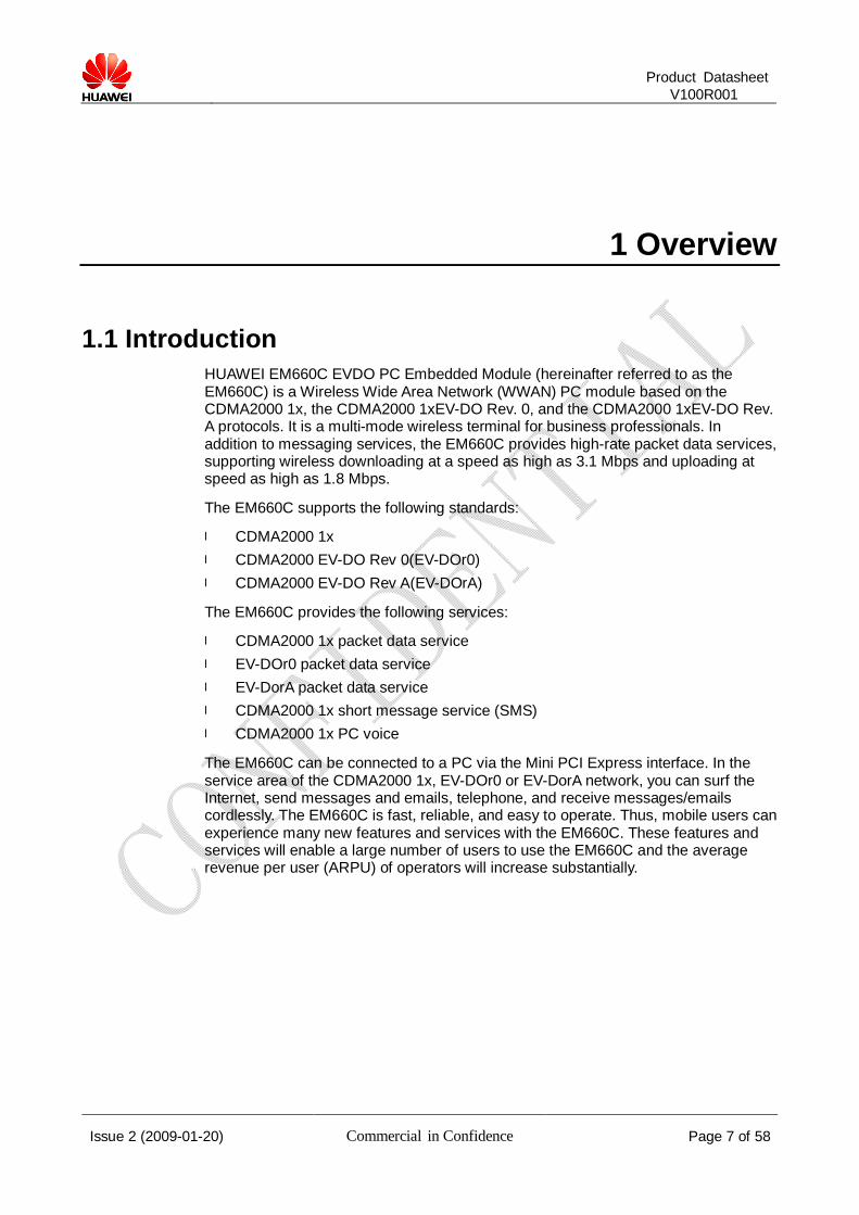
1 Overview
1.1 Introduction HUAWEI EM660C EVDO PC Embedded Module (hereinafter referred to as the EM660C) is a Wireless Wide Area Network (WWAN) PC module based on the CDMA2000 1x, the CDMA2000 1xEV-DO Rev. 0, and the CDMA2000 1xEV-DO Rev. A protocols. It is a multi-mode wireless terminal for business professionals. In addition to messaging services, the EM660C provides high-rate packet data services, supporting wireless downloading at a speed as high as 3.1 Mbps and uploading at speed as high as 1.8 Mbps.
The EM660C supports the following standards:
l CDMA2000 1x l CDMA2000 EV-DO Rev 0(EV-DOr0) l CDMA2000 EV-DO Rev A(EV-DOrA)
The EM660C provides the following services:
l CDMA2000 1x packet data service l EV-DOr0 packet data service l EV-DorA packet data service l CDMA2000 1x short message service (SMS) l CDMA2000 1x PC voice
The EM660C can be connected to a PC via the Mini PCI Express interface. In the service area of the CDMA2000 1x, EV-DOr0 or EV-DorA network, you can surf the Internet, send messages and emails, telephone, and receive messages/emails cordlessly. The EM660C is fast, reliable, and easy to operate. Thus, mobile users can experience many new features and services with the EM660C. These features and services will enable a large number of users to use the EM660C and the average revenue per user (ARPU) of operators will increase substantially.
Product Datasheet
V100R001
Issue 2 (2009-01-20) Confidencein Commercial Page 8 of 58
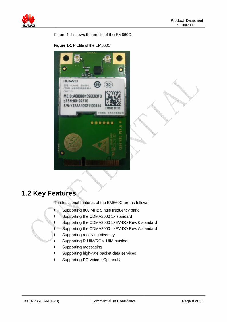
Figure 1-1 shows the profile of the EM660C.
Figure 1-1 Profile of the EM660C
1.2 Key Features The functional features of the EM660C are as follows:
l Supporting 800 MHz Single frequency band l Supporting the CDMA2000 1x standard l Supporting the CDMA2000 1xEV-DO Rev. 0 standard l Supporting the CDMA2000 1xEV-DO Rev. A standard l Supporting receiving diversity l Supporting R-UIM/ROM-UIM outside l Supporting messaging l Supporting high-rate packet data services l Supporting PC Voice(Optional)

Product Datasheet
V100R001
Issue 2 (2009-01-20) Confidencein Commercial Page 9 of 58
Table 1-1 lists the key features of the EM660C.
Table 1-1 Key features of the EM660C
Item Description
Standard l CDMA2000 1x RTT l CDMA2000 1xEV-DO Rel. 0 l CDMA2000 1xEV-DO Rev. A
Data speed l Uplink: up to 1.8 Mbit/s l Downlink: up to 3.1 Mbit/s
Uplink: 824–849 MHz Working frequency
CDMA 800 MHz
Downlink: 869–894 MHz
CDMA2000 1x RTT compliant with 3GPP2 CS0011-C: excelled -104 dBm
Receiving sensitivity
CDMA2000 1x EV-DO compliant with 3GPP2 CS0033-A: excelled -105.5 dBm
Interfaces Mini PCI Express 1.2 interface (USB 2.0 Full Speed)
Support OS Windows 2000/Windows XP/Windows Vista/Linux 2.6.18 or later versions
Maximum transmit power
CDMA 800 MHz +23 dBm(Power Class 3)
Maximum power consumption <3.3 W
Working voltage 3.0~3.6V
Dimensions (L % W % H) 51.0mm×30.0mm×5.0mm
Weight About 8 g
Operating -10 to +℃ 55℃ Ambient temperature
Storage -40℃ to +85℃
Relative humidity 5%–95%
1.3 Hardware Overview The hardware of the EM660C consists of three sections: baseband section, power management (PM) section, and radio frequency (RF) section. External interfaces include the antenna interface and the Mini PCI Express interface.

Product Datasheet
V100R001
Issue 2 (2009-01-20) Confidencein Commercial Page 10 of 58
1.3.1 Hardware Logic Block Diagram The EM660C is completed on a single-board. Figure 1-2 shows the hardware functional block diagram.
Figure 1-2 Hardware functional block diagram
The circuitry of the EM660C consists of three sections: baseband section, RF section, and PM section.
l The baseband section includes the baseband processor and DDR SDRAM/flash MCP. It implements baseband signals processing, wireless protocols, and management of various peripheral devices.
l The RF section includes the RF transceiver, PA, antenna switches, duplexer, and antenna interfaces, and it supports receive diversity.
l The PMU section includes PM Part and DC-DC circuits, providing the power supply and power management for the whole module.
1.3.2 External Hardware Interfaces 1. Antenna interface
The EM660C has a main antenna connector and an auxiliary antenna connector.

Product Datasheet
V100R001
Issue 2 (2009-01-20) Confidencein Commercial Page 11 of 58
Mini PCI Express Interface
Screw holes
Auxiliary antenna
Main antenna
2. Mini PCI Express interface
The interface of the EM660C is a standard Mini PCI Express interface. The EM660C consists of several major signals, as shown in the following figure.
Figure 1-3 Mini PCI Express identification
− RUIM interface: The RUIM interface provides the interface for a RUIM card.
The RUIM card can be inserted into the PC.

Product Datasheet
V100R001
Issue 2 (2009-01-20) Confidencein Commercial Page 12 of 58
− USB interface: This module can operate at USB low-speed (1.5 Mbits/sec) and USB full-speed (12 Mbits/sec). It is compliant with USB 2.0 Specification,and available from www.usb.org.
− Because there is not a separate USB-controlled voltage bus, USB functions implemented on EM660C which are expected to report as self-powered devices.
− Auxiliary signals: The auxiliary signals provide some other functions. − Power sources and grounds: The PCI Express Mini Card provides two power
sources, including the one at +3.3 Vaux (3.3Vaux) and the one at 1.5 V(+1.5 V). The EM660C uses the +3.3 voltage as the power supply.
1.4 Software Overview Descriptions of the functional modules in the system architecture are as follows
Figure 1-4 Software logic block diagram
.
Dashboard
PC Drivers
Application Service Subsystem
Firmware Drivers
Platform Service Subsystem
PC
Firmware
Mini PCIE interface
Firmware
PC Drivers
Dashboard

Product Datasheet
V100R001
Issue 2 (2009-01-20) Confidencein Commercial Page 13 of 58
Firmware Drivers The firmware drivers include drivers of the RF module, flash, and all the peripherals such as the UIM card and USB device.
Platform Service Subsystem The platform service subsystem initializes programs, diagnoses, downloads data, and serves as a watchdog.
Application Service Subsystem The application service subsystem consists of various application services and a CDMA 1X/EVDO dual mode protocol stack. Application services handle the commands and data received from PC side according to service categories, and deliver them to the protocol stack. The protocol stack communicates with the network side to process the commands and data, and returns response from network to application services. Finally, application services return responses to PC side.
The main application services are as follows:
l Call management service l SMS service l 1X/EVDO data service
PC Drivers The PC drivers are used to implement functions such as the interaction between the dashboard and the firmware.
Dashboard The dashboard enables the PC side to display the interfaces of initiating or answering a call, and sending and receiving messages. It provides the interface for 1X/EVDO network accessing and periodically refreshes the interface of the current USB modem status. The interface is provided to the end users.

Product Datasheet
V100R001
Issue 2 (2009-01-20) Confidencein Commercial Page 14 of 58
2 Mechanical Specifications
2.1 Dimensions and interfaces 2.1.1 Dimensions and interfaces of the EM660C
The dimensions of the EM660C are 51 mm (length) × 30 mm (width) × 5 mm (height), which comply with the standard dimensions specified in the PCI Express Mini Card Electromechanical Specification Revision 1.2. Figure 2-1 shows the dimensions of the EM660C in details.
Figure 2-1 Dimensions of the EM660C
Figure 2-2 shows the appearance of the interfaces on the EM660C.

Product Datasheet
V100R001
Issue 2 (2009-01-20) Confidencein Commercial Page 15 of 58
Figure 2-2 Appearance of the interfaces on the EM660C
1
3
2
2
Mini PCI Express connector
It is used to connect the EM660C to the WWAN Mini PCI Express interface of the PC.
Screw holes
They are used to fix the EM660C on the main board of the PC with screws.
Antenna interfaces
They are used to connect to antennas. Auxiliary antenna and main antenna are combined to support receive diversity. The receive diversity can strengthen the received RF signal quality and improve RF performance, and whether to open or close the receive diversity function can be controlled by software.
Notes:
We strongly recommend adding auxiliary antenna when you design PC with the EM660C.
2.1.2 Dimensions of the Mini PCI Express Connector The EM660C adopts a standard Mini PCI Express connector that has 52 pins and complies with the PCI Express Mini Card Electromechanical Specification Revision 1.2.
Figure 2-3 shows a 52-pin Mini PCI Express connector (take the Molex 67910002 as an example).

Product Datasheet
V100R001
Issue 2 (2009-01-20) Confidencein Commercial Page 16 of 58
Figure 2-3 Dimensions of the Mini PCI Express connector
2.1.3 Dimensions of the Antenna Connector The EM660C provides an interface for connecting an external antenna. The external antenna is connected to the module through the coaxial connector that is the Hirose U.FL-R-SMT-1(10) (you can get to know Hirose U.FL-R-SMT-1(10) by visiting the website http://www.hirose-connectors.com/products/U.FL_1.htm).

Product Datasheet
V100R001
Issue 2 (2009-01-20) Confidencein Commercial Page 17 of 58
Figure 2-4 Dimensions of the antenna connector
Figure 2-5 shows the specifications of the antenna mating connectors (take the ones with the Hirose part number as U.FL-LP as examples).
Figure 2-5 Specifications of the antenna mating connectors
For more information about Hirose Ltd., SMD connectors, and mating connectors, visit the website of Hirose http://www.hirose-connectors.com.

Product Datasheet
V100R001
Issue 2 (2009-01-20) Confidencein Commercial Page 18 of 58
2.2 Reliability Table 2-1 Requirements on the environment reliability
Test Case Standard
High temperature IEC60068-2-2
High temperature IEC60068-2-1
Random vibration MIL-STD-810F -METHOD 514.5
Shock vibration ANSI/TIA-603-C-2004 -3.3.5
Operational
Sine sweep vibration ANSI/TIA-603-C-2004 -3.3.4
High temperature IEC60068-2-2
Low temperature IEC60068-2-1
Damp heat, cyclic IEC60068-2-30
Thermal shock IEC60068-2-14
Salt-fog IEC60068-2-11
Drop IEC 60068-2-32
Environment reliability
Non-operational
Durability EIA-364-9
2.3 Temperature Table 2-2 Operating and storage temperature
Description Minimum Maximum Unit
Operating temperature –10 +55 ℃
Storage temperature –40 +85 ℃

Product Datasheet
V100R001
Issue 2 (2009-01-20) Confidencein Commercial Page 19 of 58
3 Electrical Specifications
3.1 Mini PCI Express Pin Definition The physical connections and signal levels of the EM660C comply with PCI Express Mini CEM specifications. Device operations comply with USB 2.0 specifications.
Table 3-1 lists the Mini PCI Express connector pins out of the EM660C.
Table 3-1 Definition of mini PCI Express pins
Definition of the EM660C Mini PCI Express pins
Pin No.
Mini PCI Express Standard Description
HUAWEI Pin Description
Additional Description
Direction to Module
1 WAKE# NC Not connected. –
2 3.3Vaux VCC_3V3 3.3 V DC supply rails from the PC side.
Input
3 COEX1 NC Not connected. –
4 GND GND Mini Card ground. –
5 COEX2 NC Not connected. –
6 1.5 V NC Not connected. –
7 CLKREQ# NC Not connected. –
8 UIM_PWR UIM_PWR Power source for the external UIM/UIM card.
Output
9 GND GND Mini Card ground. –
10 UIM_DATA UIM_DATA External UIM/UIM data signal.
Input/Output
11 REFCLK- NC Not connected. –
12 UIM_CLK UIM_CLK External UIM/UIM clock signal.
Output
13 REFCLK+ NC Not connected. –

Product Datasheet
V100R001
Issue 2 (2009-01-20) Confidencein Commercial Page 20 of 58
Definition of the EM660C Mini PCI Express pins
Pin No.
Mini PCI Express Standard Description
HUAWEI Pin Description
Additional Description
Direction to Module
14 UIM_RESET UIM_RESET External UIM/UIM reset signal.
Output
15 GND GND Mini Card ground. –
16 UIM_Vpp NC Not connected. –
17 Reserved NC Not connected. –
18 GND GND Mini Card ground. –
19 Reserved NC Not connected. –
20 W_DISABLE# W_DISABLE_N For ending the wireless communications
Input
21 GND GND Mini Card ground. –
22 PERST# PERST# For forcing a hardware reset on the card.
Input
23 PERn0 NC Not connected. –
24 3.3Vaux NC Not connected. –
25 PERp0 NC Not connected. –
26 GND GND Mini Card ground. –
27 GND GND Mini Card ground. –
28 1.5 V NC Not connected. –
29 GND GND Mini Card ground. –
30 SMB_CLK NC Not connected. –
31 PETn0 NC Not connected. –
32 SMB_DATA NC Not connected. –
33 PETp0 NC Not connected. –
34 GND GND Mini Card ground. –
35 GND GND Mini Card ground. –
36 USB_D- USB_D- USB signal D-. Input/Output
37 GND GND GND –
38 USB_D+ USB_D+ USB signal D+. Input/Output

Product Datasheet
V100R001
Issue 2 (2009-01-20) Confidencein Commercial Page 21 of 58
Definition of the EM660C Mini PCI Express pins
Pin No.
Mini PCI Express Standard Description
HUAWEI Pin Description
Additional Description
Direction to Module
39 3.3Vaux VCC_3V3 3.3V DC supply rail from the PC side.
Input
40 CPUSB# GND GND –
41 3.3Vaux VCC_3V3 3.3V DC supply rail from the PC side.
Input
42 LED_WWAN# LED_WWAN Active-low LED signal for indicating the state of the card.
Output
43 GND GND GND –
44 LED_WLAN# NC Not connected. –
45 Reserved PCM_CLK PCM clock Output
46 LED_WPAN# NC Not connected. –
47 Reserved PCM_DOUT PCM data output Output
48 1.5 V NC Not connected –
49 Reserved PCM_DIN PCM_data input Input
50 GND GND Mini Card Ground –
51 Reserved PCM_SYNC PCM frame synchronization
Output
52 3.3Vaux VCC_3V3 3.3V DC supply rail from the PC side.
Input

Product Datasheet
V100R001
Issue 2 (2009-01-20) Confidencein Commercial Page 22 of 58
3.2 Pin Descriptions 3.2.1 Digital Signal DC Characteristics
Table 3-2 Digital signal DC characteristics
Symbol Description Minimum Maximum Unit Notes
VIH High-level input voltage, CMOS/Schmitt
0.65* VDD_PX
VDD_PX +0.3
V 1
VIL Low-level input voltage, CMOS/Schmitt
–0.3 0.35-VDD_PX
V 1
VOH High-level output voltage, CMOS
VDD_PX-0.45
VDD_PX V 1
VOL Low-level output voltage, CMOS
0 0.45 V 1
IIH Input high leakage current – 1 µA 1
IIL Input low leakage current –1 – µA 1
IIHPD Input high leakage current with pull-down
3 30 µA 1
IILPU Input low leakage current with pull-up
–30 –3 µA 1
IOZH High-level, three-state leakage current
– 1 µA 1
IOZL Low-level, three-state leakage current
–1 – µA 1
IOZHPD High-level, three-state leakage current with pull-down
3 30 µA 1
IOZLPU Low-level, three-state leakage current with pull-up
–30 –3 µA 1
CIN Input capacitance – 7 pF 1, 2
Notes:
1. Table 3-2 lists the universal specifications of the signals. Any difference from the universal specifications is listed in the related chapter or section.
2. The input capacitance value is guaranteed by design and not completely tested.

Product Datasheet
V100R001
Issue 2 (2009-01-20) Confidencein Commercial Page 23 of 58
3.2.2 Power Sources and Grounds The PCI Express Mini Card provides two power sources: one is +3.3Vaux (3.3 Vaux) and the other is 1.5V (+ 1.5 V). For the EM660C, +3.3Vaux is the only supply voltage available. The input voltage is +3.3 V ± 9%, as specified by PCI Express Mini CEM Specifications 1.2.
Table 3-3 Power and ground specifications
Name Pins Minimum Type Maximum
VCC 2, 39, 41, and 52 3.0 V 3.3 V 3.6 V
GND 4, 9, 15, 18, 21, 26, 27, 34, 35, 37, 43, and 50
0 V
3.2.3 USB Signals The EM660C is compliant with USB 2.0 specification. It supports full-speed and low-speed.
Table 3-4 USB pins
Name Pin Description Direction to Module
USB D- 36 USB data signal D- Input/Output
USB D+ 38 USB data signal D+ Input/Output
The USB interface is powered directly from the 3.3 V supply. The USB input/output lines are compatible with the USB 2.0 3.3 V signal specifications.
Table 3-5 USB signal DC characteristics
VOHmin VOLmax VIHmin VILmax
2.8V 0.3V 2V 0.8V
3.2.4 RUIM Signals The RUIM is a smart card for CDMA cellular applications; it provides personal authentication information that allows the mobile station or handset to be connected with the network. The RUIM card can be inserted into any CDMA RUIM equipped handset to enable its user to receive or make calls and receive other subscribed services.
The internal power management circuits, UIM circuity, and UIM pads allow for implementing both 1.8 V and/or 2.85 V cards via a direct connection.

Product Datasheet
V100R001
Issue 2 (2009-01-20) Confidencein Commercial Page 24 of 58
Key RUIM features are:
l Shared interface for RUIM applications, thereby further supporting CDMA networks
l Selectable clock source l Supports dual voltage cards (2.85 V and 1.8 V)
Product Datasheet
V100R001
Issue 2 (2009-01-20) Confidencein Commercial Page 25 of 58
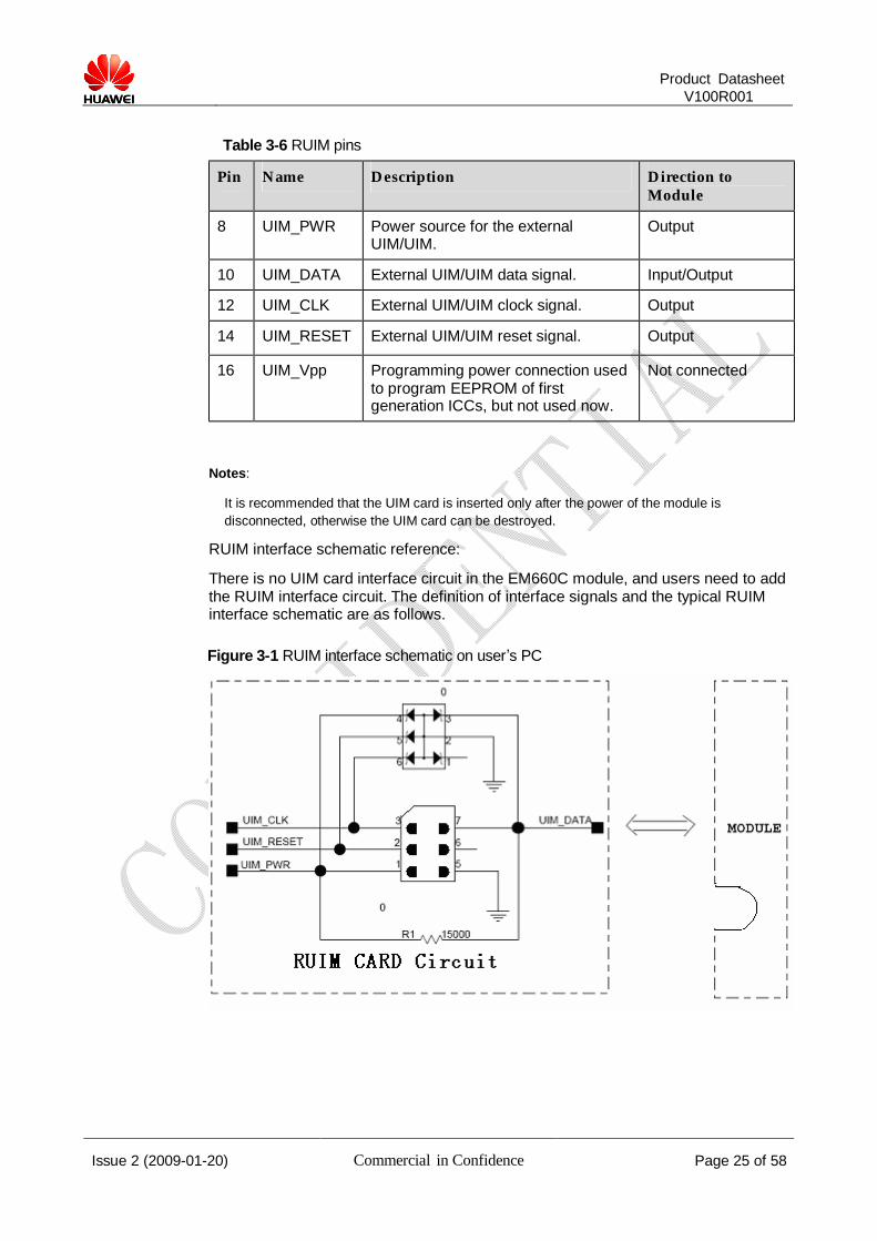
Table 3-6 RUIM pins
Pin Name Description Direction to Module
8 UIM_PWR Power source for the external UIM/UIM.
Output
10 UIM_DATA External UIM/UIM data signal. Input/Output
12 UIM_CLK External UIM/UIM clock signal. Output
14 UIM_RESET External UIM/UIM reset signal. Output
16 UIM_Vpp Programming power connection used to program EEPROM of first generation ICCs, but not used now.
Not connected
Notes:
It is recommended that the UIM card is inserted only after the power of the module is disconnected, otherwise the UIM card can be destroyed.
RUIM interface schematic reference:
There is no UIM card interface circuit in the EM660C module, and users need to add the RUIM interface circuit. The definition of interface signals and the typical RUIM interface schematic are as follows.
Figure 3-1 RUIM interface schematic on user’s PC

Product Datasheet
V100R001
Issue 2 (2009-01-20) Confidencein Commercial Page 26 of 58
Design guide
The RUIM signals are connected to the Mini PCI Express card connector (the card edge connector) and pass through an EMI filtering and ESD protection circuit on the module board before entering the EM660C processor. There is also an EMI filtering and ESD protection circuit between UIM card interface and Mini PCI interface on the user’s board.
1. Power supply
The UIM interface is powered by an LDO regulator. The default value of this regulator is 2.85 V. The power of the regulator is programmable in the range of 1.5 V to 3.05 V and is expected to be set to 2.85 V or 1.8 V.
2. Modem signals
After a power-on or reset, the RUIM signals are activated to detect if a UIM card is present and to initialize it if it exists. Once a card has been detected and initialized, the interface is always on. However, the clock signal is only activated when data is actually being transferred. The RUIM signals from the MSM are connected to the level translators and then to the Mini Card host connector.
These levels exceed those required in ISO/IEC 7816-3.
3. ESD protection
Since the UIM is a CMOS device, ESD protection devices should be placed near to the UIM connector to provide protection. In addition, all the UIM interface signals should be bypassed with a 33 pF capacitor.
4. Routing recommendations
The UIM interface signals consist of four signals that are Vcc, RST, CLK, and IO (Vpp is also connected but not used in many applications). Due to the relatively low clock frequencies involved, the concern is not the degradation of the UIM signals themselves. The main concern is routing of the UIM interface signals through areas considered to be of high risk for RF noise coupling (crosstalk and RF contamination) which can desensitize the radio circuitry. The general guidelines that should be followed are listed as follows:
l It is recommended that these signals should be routed over a contiguous ground plane.
l UIM interface signals should not be routed near high transient signals (power supply chokes and DC/DC switching FETs).
l Avoid routing of these signals near output connectors. l Keep UIM interface signals isolated from other signals. 2x width spacing (1.5x
min) between UIM interface signals and all other signal routing is recommended.

Product Datasheet
V100R001
Issue 2 (2009-01-20) Confidencein Commercial Page 27 of 58
3.2.5 W_DISABLE# Signal The W_DISABLE# signal is provided to allow users to disable wireless communications add-in cards. When the W_DISABLE# signal is asserted, all radios should be disabled. When the W_DISABLE# signal is not asserted, the radio may transmit if not disabled by other means such as software.
The W_DISABLE# signal is an active low signal with internal 100 kΩ pull-up resistor that shall disable radio operation when being asserted (driven low) by the system.
Due to the potential of a software disable state, the combination of the software state and W_DISABLE# assertion state must be determined before the normal operation is resumed. Table 3-8 lists this requirement on the function of W_DISABLE# and the software control setting. For example, the radio RF operation remains disabled unless both the hardware and software are set to enable the RF features of the card.
Table 3-7 W_DISABLE_N signal
Pins Name Description Direction to Module
20 W_DISABLE_N Close wireless communications Input
Table 3-8 Radio operational states
W_DISABLE# SW Control Setting* Radio Operation
High Enabled Enabled
High Disabled
Low Enabled
Low Disabled
Disabled
* This control setting is implementation specific; this column represents the collective intention of the host software to manage radio operation.
Notes:
We strongly recommend controlling this pin via hot-keys or a hardware switch. There are three points as bellow:
1. If we don’t turn off radio manually, radio will be on when module is powered on.
2. End users need turn off radio at some situation like on an airplane.
3. According to Mini-PCIE specification, we must turn off radio through hardware or software. Nearly all PC companies obey this specification.
3.2.6 LED_WWAN# Signal The LED_WWAN signal of the EM660C can tolerate up to the voltage of 5 V and absorb the current up to150 mA. According to the given circuit, in order to reduce the current of the LED, a resistance of 1 kΩ must be placed in series with the LED.

Product Datasheet
V100R001
Issue 2 (2009-01-20) Confidencein Commercial Page 28 of 58
Table 3-9 LED_WWAN signal
Pins Name Description Additional Description
Direction to Module
42 LED_WWAN Active-low LED signal for indicating the status of the module.
L: Light on H: Light off
Output
This signal is used to display the state of WWAN. The reference circuit diagram is shown in the following figure.
Figure 3-2 LED_WWAN# signal reference circuit diagram
Notes:
The wink mode of the LED can be customized by the demand of the client.
3.2.7 PERST# Signal The PERST# signal has an internal pull-up. The active low input is used to hard reset the module.
The PERST# signal is de-asserted by the host to indicate that system power sources are within the specified voltage tolerance and are stable. PERST# can be asserted by the host when power is switched off and also can be used by the system to force a hardware reset on the card. However, a hardware reset is not required during normal operation and may only be used in case of module malfunction.
A hard reset of the module will result in a surprise removal of the module on the USB controller and cause the operating system to unload the device drivers. This will lead to a delay before the operating system discovers the device again. To avoid this delay, the PERST# pin should not be used in normal operation or in standby mode.
100 n
1 kΩ LED
Module
VCC
LED_WWAN signal
1 kΩ
PC

Product Datasheet
V100R001
Issue 2 (2009-01-20) Confidencein Commercial Page 29 of 58
Table 3-10 PERST# signal
Pins Name Description Additional Description
Direction to Module
22 PERST# Force a hardware reset on the card.
H: normal or standby. L: Reset the module.
Input
3.2.8 NC Pins The NC pins are not internally connected in the EM660C.
3.3 Power Supply and Consumption 3.3.1 Power Supply
The EM660C is supplied by 3.3 V power source, which must satisfy all requirements of PCI Express Mini CEM specifications, such as voltage tolerance and peak and normal current. The detailed requirements are listed in Table 3-11.
Table 3-11 Power requirements
Power Voltage Tolerance Peak (Maximum) Normal (Maximum)
3.3 V ±9% 2750 mA 1100 mA
Notes:
To minimize the RF radiation through the PCI-E interface, you can add a 33 pF ceramic capacitor to ground on every pin of the PCI-E on the host side except USB D+/D-.
3.3.2 Power Consumption The power consumptions of the EM660C in different scenarios are respectively listed in Table 3-12, and Table 3-14.

Product Datasheet
V100R001
Issue 2 (2009-01-20) Confidencein Commercial Page 30 of 58
Table 3-12 DC power consumption (CDMA)
Band Frequency Channel
Test Value Units Power (dBm)
218 1dBm Tx Power
303 10dBm Tx Power 384
577
mA
24dBm Tx Power
215 1dBm Tx Power
311 10dBm Tx Power 777
580
mA
23.6dBm Tx Power
217 1dBm Tx Power
323 10dBm Tx Power
BAND0 (Cell 800M)
1013
648
mA
23.7dBm Tx Power
Table 3-13 DC power consumption (EVDO)
Band Frequency Channel
Test Value Units Power (dBm)
299 1dBm Tx Power
325 10dBm Tx Power 384
600
mA
24.3dBm Tx Power
304 1dBm Tx Power
331 10dBm Tx Power 777
627
mA
24dBm Tx Power
300 1dBm Tx Power
341 10dBm Tx Power
BAND0 (Cell 800M)
1013
645
mA
23.9dBm Tx Power
Table 3-14 DC power consumption(Idle and Suspend)
Suspend Scenario
Offline Enabled Offline Disabled
Unit
CDMA2000 1X 2.80 4.10 mA
EVDO 2.80 4.58 mA

Product Datasheet
V100R001
Issue 2 (2009-01-20) Confidencein Commercial Page 31 of 58
Notes:
The EM600 module has three different operating mode:
1:active mode;
2:suspend mode ;
3:power off mode.

Product Datasheet
V100R001
Issue 2 (2009-01-20) Confidencein Commercial Page 32 of 58
4 RF Specifications
4.1 Operating Frequencies Table 4-1 RF bands
EM660C
Operating Band Tx Rx
CDMA Cellular 824–849 MHz 869–894 MHz
4.2 Conducted Rx sensitivity and Tx power Table 4-2 EM660C conducted Rx sensitivity
Item 3GPP Protocol Claim Unit
CDMA Cellular <–104 dBm
Table 4-3 EM660C conducted Tx power
Item 3GPP Protocol Claim Unit
CDMA Cellular >23 dBm
% = Bit Error Rate or Block Error Rate
4.3 Antenna Design Requirements 4.3.1 Recommended Index of the Module Antennas
Table 4-4 Recommended index of the main antenna
Working frequency 824–849 MHz and 869–894 MHz
Port impedance 50 Ohm
Port standing wave < 2.0
Product Datasheet
V100R001
Issue 2 (2009-01-20) Confidencein Commercial Page 33 of 58
Peak gain > 0 dBi
Antenna efficiency > 60%
Polarization Linear polarization
Pattern Omnidirectional
Table 4-5 Recommended index of the auxiliary antenna
Working frequency 869–894 MHz,
Port impedance 50 Ohm
Port standing wave < 2.0
Peak gain > –3 dBi
Antenna efficiency > 30%
Polarization Linear polarization
Pattern Omnidirectional
Table 4-6 Recommended index of the isolation between the main antenna and the auxiliary antenna
Antenna isolation < –10 dB
Because the PC has other internal antennas such as the WLAN antenna, to ensure the proper operation of each communication system, requirements on antenna isolation between different communication systems should be considered. Table 4-7 lists the recommended index of the antenna isolation.
Table 4-7 Recommended index of the isolation between the module antennas and other PC antennas
Antenna isolation < –20 dB
4.3.2 Design Recommendations
Recommendations for Designing the Module Antennas The design recommendations are as follows:
1. It is recommended that the module antennas are designed at the upper edge, left edge or right edge of the PC screen. Designing the antenna at the upper edge is better.
2. When designing the main antenna and the auxiliary antenna, the requirement on the antenna isolation should be considered (the recommended value is listed in Table 4-6). Meanwhile, try to keep the distance between the main antenna and the auxiliary antenna as large as possible for optimizing the space diversity. For

Product Datasheet
V100R001
Issue 2 (2009-01-20) Confidencein Commercial Page 34 of 58
example, you can place the main antenna at the upper left corner of the PC screen and place the auxiliary antenna at the upper right corner of the PC screen.
3. You are recommended to design the antenna pattern as the horizontal polarized omnidirectional pattern that facilitates the reception of strong signals especially in outdoor environments.
4. Besides the module antennas, a PC has other internal antennas, such as the WLAN antenna. Therefore, when designing the module antennas, the requirement on the isolation between module antennas and other PC antennas should be considered (the recommended value is listed in Table 4-7). Keep proper distance between antennas if possible. To reduce the interference between antennas, it is not recommended that an antenna is designed closely next to another one.
5. Carefully design the metallic components (such as the external frame of the metallic shell) in and near the antenna area with considering the effects on the antenna performance (such as whether the frequency offset of the antenna occurs and whether the antenna pattern is deformed).
Recommendations for Handling the Interference Sources On a PC, there are various interference sources, such as the LCD, CPU, audio circuits, and power supply. All the interference sources emit interference signals that affect the normal operation of the module. For example, the module sensitivity can be decreased due to interference signals. Therefore, during the design, you need to consider how to lessen the effects of interference sources on the module. You can take the following measures: Use an LCD with optimized performance; shield the LCD interference signals; shield the signal cable of the PC; or design filter circuits.
4.4 Offline Mode The offline mode can be enabled by the following method:
l Through hardware: The W_DISABLE pin can be used to control the RF circuit. When the pin is driven to the high level, the RF circuit works; when the pin is driven to the low level, the RF circuit does not work.

Product Datasheet
V100R001
Issue 2 (2009-01-20) Confidencein Commercial Page 35 of 58
5 Software and Tools
Huawei can provide the firmware, PC driver, dashboard, and software. The firmware runs on the module; the PC driver and dashboard run on the PC and communicate with the firmware to realize all module functions. Huawei can also provide the software for upgrading the firmware and debugging the problems.
5.1 Firmware The firmware is software on the module. It accepts commands and data from the host through USB. The host can send AT commands to enable the firmware to connect, disconnect, or query.
5.1.1 Version Descriptions In the version number, the front digits is the firmware version that can differ which version is newer. The upper bits (except the last two bits) has boarder meaning in the version name. If the customer has special order to our common version, the order will be implemented in special version. The version is named by last two bits, but the front bits are still the common version.
5.2 Drivers A driver is a program running on the host system, which allows the host system to interact with the Huawei wireless module. The driver communicates with the firmware of the module by using the USB protocol.
The USB manufacturer ID for all Huawei USB devices is 0x12D1.
The USB product ID for the EM660C device is 0x1001. There are three USB interfaces in the USB product ID.
XX.XXX.XX.XX.XX
Firmware version Customization version

Product Datasheet
V100R001
Issue 2 (2009-01-20) Confidencein Commercial Page 36 of 58
5.2.1 Windows Drivers Huawei provides windows drivers to support Windows 2000/XP/Vista.
Huawei provides the following two ways to install the drivers:
l The drivers are packed in the dashboard, and they will be installed during the dashboard installation.
l The drivers are provided as an installer, which can be directly installed under Windows 2000/XP/Vista.
After the drivers are installed, when the EM660C is connected to the USB bus, it will be detected as a USB device and start enumerating. During this process, multiple drivers are loaded. These drivers expose a number of virtual COM ports.
In Windows OSs, you can check the enumerated devices and their configuration in the device manager. If you switch to View by connection, the device manager displays the main USB device and interfaces, as shown in Figure 5-1, this figure is just a sample, different products maybe add or remove some ports.
Figure 5-1 HUAWEI USB device and interfaces
The following interfaces and ports are supported by EM660C:
l HUAWEI Mobile Connect – 3G Modem: used to set up a data connection. l HUAWEI Mobile Connect – 3G Application Interface: used to write and read
diagnostics data. l HUAWEI Mobile Connect – 3G PC UI Interface: used to send AT commands and
read their responses.
5.2.2 Linux Drivers The EM660C can be used in the Linux OS that the kernel version is 2.6.18 or later. If the kernel is a standard one, it means that the kernel is not customized and the driver

Product Datasheet
V100R001
Issue 2 (2009-01-20) Confidencein Commercial Page 37 of 58
is already packed in the kernel; if the kernel is customized and the driver has been discarded, Huawei will provide the Linux driver for customers to merge the driver into the kernel again.
5.3 Dashboard 5.3.1 Windows Dashboard
Huawei can provide the dashboard to manage the connection and other functions under Windows 2000/XP/Vista.
Figure 5-2 shows the screenshot of Huawei common dashboard.
Figure 5-2 Screenshot of Huawei common dashboard
Table 5-1 lists the dashboard specifications.
Table 5-1 Windows dashboard specifications
Item Description
Writing/Sending/Receiving
Sending/Receiving the SMS
SMS
Group sending

Product Datasheet
V100R001
Issue 2 (2009-01-20) Confidencein Commercial Page 38 of 58
Item Description
New message prompt (visual prompt/audio prompt)
Current connection: l Duration l Send/Receive flow l Send/Receive rate
Flow display and statistics (data services)
Traffic statistics: You can view the traffic information of the day, the month, or the year.
Stores the contacts in the hard disk of the PC, the UIM card and the device.
Messages can be sent through the phonebook.
Phonebook
Importing/Exporting: Import or export contacts between the UIM card and a PC or a file of supported formats.
Network connection setup
l Profile management: create, delete, and edit. l Set up the network connection.
Network status display
Signal status, system mode, and so on.
network connection types
Selection of network connection types, for example: l 1X only l EVDO only l Hybrid
PIN management
Activating or deactivating PIN, PIN lock, changing PIN, and unblocking PIN by using the PUK
System requirement
l Windows 2000 SP4, Windows XP SP2, Windows Vista l The hardware system on the PC should meet or exceed the
recommended system requirements for the installed version of OS.
l Display resolution: 800 × 600 or above
Notes: CPU = central processing unit PIN = personal identification number PUK = PIN unblocking key
5.3.2 Linux Dashboard The Linux dashboard can be developed separately according to the customization requirements of customers.

Product Datasheet
V100R001
Issue 2 (2009-01-20) Confidencein Commercial Page 39 of 58
5.4 Tools 5.4.1 Firmware Update Tool
The Windows-based update tool provided by Huawei is used to update the firmware of the EM660C.
The following figures (from Figure 5-3 to Figure 5-9)show the procedure for using the EM660C update tool.The EM660C update procedure is the same as EM660C.
Figure 5-3 EM660C update tool

Product Datasheet
V100R001
Issue 2 (2009-01-20) Confidencein Commercial Page 40 of 58
Figure 5-4 Screenshot of the EM660C update tool–Searching the device
Figure 5-5 Screenshot of the EM660C update tool–Detected devices

Product Datasheet
V100R001
Issue 2 (2009-01-20) Confidencein Commercial Page 41 of 58
Figure 5-6 Screenshot of the EM660C update tool–Warning
Figure 5-7 Screenshot of the EM660C update tool–Downloading programs

Product Datasheet
V100R001
Issue 2 (2009-01-20) Confidencein Commercial Page 42 of 58
Figure 5-8 Screenshot of the EM660C update tool–Update succeeded
Figure 5-9 Screenshot of the EM660C update tool–To finish the update
Product Datasheet
V100R001
Issue 2 (2009-01-20) Confidencein Commercial Page 43 of 58
5.4.2 Engineering Tools Qualcomm has an extensive debugging and tracing toolset available for their chipsets. Huawei EM660C is compatible with these tools from Qualcomm, such as QXDM, QPST, and QCAT.
5.4.3 Debugging Board I. Functions and Usage of the Debugging board
The debugging board developed by Huawei is an auxiliary board that is used to debug the EM660C.When the debugging board is used, you can connect the module to a PC through a USB cable. When the module works normally, the debugging functions can be implemented. The debugging board provides multiple interfaces, such as the USB port, DC power jack, mini PCI-E connector, BTB connector, UIM card socket, RF connectors, PCM audio interface, and serial ports (including a 4-pin serial port and a serial port that all pins are led out). The test points of key signals are led out on the debugging board. In addition, the debugging board is designed with switches or pins of commonly used signals such as the reset signal and the enable signal, for converting the working state of the module.
The debugging board can be used to test the performance of the module. Both the wired connection test (connect the module to the CMU200) and the wireless connection test (connect the module to the antennas) can be implemented. The signal points can also be tested when you maintain and repair the module.
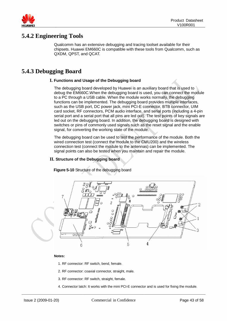
II. Structure of the Debugging board
Figure 5-10 Structure of the debugging board
Notes:
1. RF connector: RF switch, bend, female.
2. RF connector: coaxial connector, straight, male.
3. RF connector: RF switch, straight, female.
4. Connector latch: It works with the mini PCI-E connector and is used for fixing the module.
Product Datasheet
V100R001
Issue 2 (2009-01-20) Confidencein Commercial Page 44 of 58
5. Mini PCI-E connector: female, 52-pin, straight.
6. UIM card socket: It is used to holding the inserted UIM card.
7. USB connector and mini USB B-type receptacle: Side-plugging USB connector.
III. Method for Connecting the Debugging Board
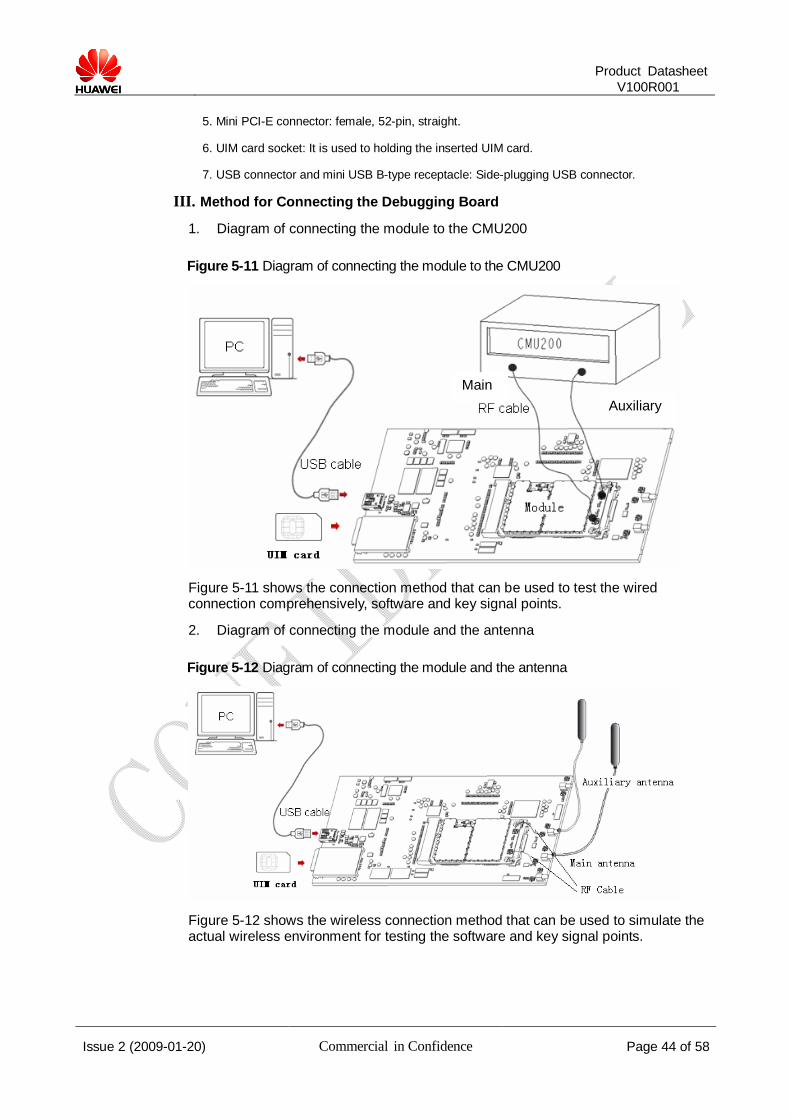
1. Diagram of connecting the module to the CMU200
Figure 5-11 Diagram of connecting the module to the CMU200
Figure 5-11 shows the connection method that can be used to test the wired connection comprehensively, software and key signal points.
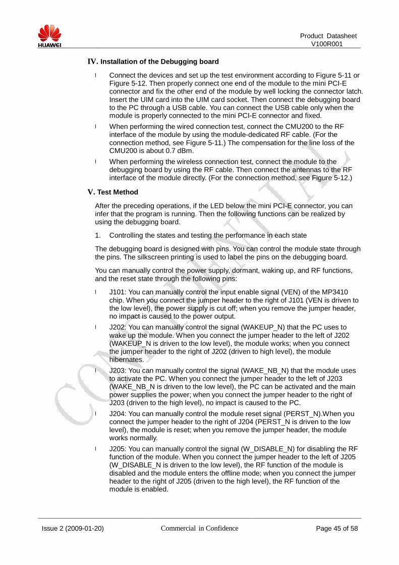
2. Diagram of connecting the module and the antenna
Figure 5-12 Diagram of connecting the module and the antenna
Figure 5-12 shows the wireless connection method that can be used to simulate the actual wireless environment for testing the software and key signal points.
Auxiliary Main
Product Datasheet
V100R001
Issue 2 (2009-01-20) Confidencein Commercial Page 45 of 58
IV. Installation of the Debugging board
l Connect the devices and set up the test environment according to Figure 5-11 or Figure 5-12. Then properly connect one end of the module to the mini PCI-E connector and fix the other end of the module by well locking the connector latch. Insert the UIM card into the UIM card socket. Then connect the debugging board to the PC through a USB cable. You can connect the USB cable only when the module is properly connected to the mini PCI-E connector and fixed.
l When performing the wired connection test, connect the CMU200 to the RF interface of the module by using the module-dedicated RF cable. (For the connection method, see Figure 5-11.) The compensation for the line loss of the CMU200 is about 0.7 dBm.
l When performing the wireless connection test, connect the module to the debugging board by using the RF cable. Then connect the antennas to the RF interface of the module directly. (For the connection method, see Figure 5-12.)
V. Test Method
After the preceding operations, if the LED below the mini PCI-E connector, you can infer that the program is running. Then the following functions can be realized by using the debugging board.
1. Controlling the states and testing the performance in each state
The debugging board is designed with pins. You can control the module state through the pins. The silkscreen printing is used to label the pins on the debugging board.
You can manually control the power supply, dormant, waking up, and RF functions, and the reset state through the following pins:
l J101: You can manually control the input enable signal (VEN) of the MP3410 chip. When you connect the jumper header to the right of J101 (VEN is driven to the low level), the power supply is cut off; when you remove the jumper header, no impact is caused to the power output.
l J202: You can manually control the signal (WAKEUP_N) that the PC uses to wake up the module. When you connect the jumper header to the left of J202 (WAKEUP_N is driven to the low level), the module works; when you connect the jumper header to the right of J202 (driven to high level), the module hibernates.
l J203: You can manually control the signal (WAKE_NB_N) that the module uses to activate the PC. When you connect the jumper header to the left of J203 (WAKE_NB_N is driven to the low level), the PC can be activated and the main power supplies the power; when you connect the jumper header to the right of J203 (driven to the high level), no impact is caused to the PC.
l J204: You can manually control the module reset signal (PERST_N).When you connect the jumper header to the right of J204 (PERST_N is driven to the low level), the module is reset; when you remove the jumper header, the module works normally.
l J205: You can manually control the signal (W_DISABLE_N) for disabling the RF function of the module. When you connect the jumper header to the left of J205 (W_DISABLE_N is driven to the low level), the RF function of the module is disabled and the module enters the offline mode; when you connect the jumper header to the right of J205 (driven to the high level), the RF function of the module is enabled.
Product Datasheet
V100R001
Issue 2 (2009-01-20) Confidencein Commercial Page 46 of 58
Though controlling the module states manually, you can test the performance and parameter in each state by using the CMU200 or other matching software.
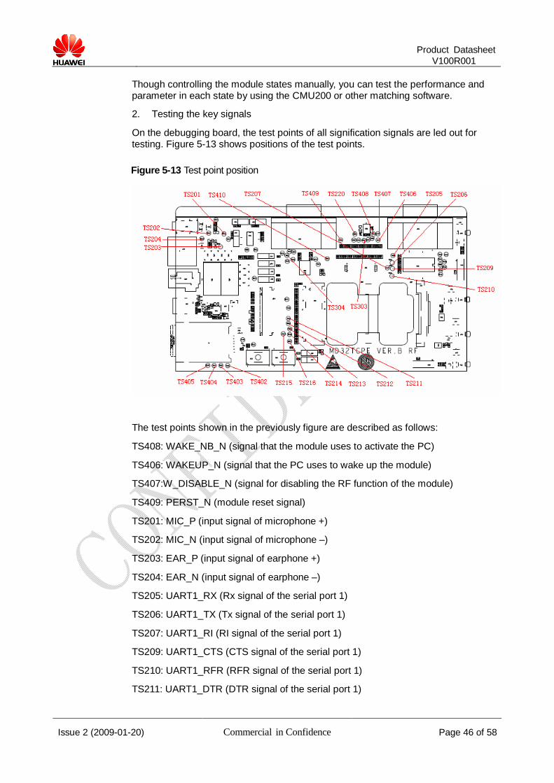
2. Testing the key signals
On the debugging board, the test points of all signification signals are led out for testing. Figure 5-13 shows positions of the test points.
Figure 5-13 Test point position
The test points shown in the previously figure are described as follows:
TS408: WAKE_NB_N (signal that the module uses to activate the PC)
TS406: WAKEUP_N (signal that the PC uses to wake up the module)
TS407:W_DISABLE_N (signal for disabling the RF function of the module)
TS409: PERST_N (module reset signal)
TS201: MIC_P (input signal of microphone +)
TS202: MIC_N (input signal of microphone –)
TS203: EAR_P (input signal of earphone +)
TS204: EAR_N (input signal of earphone –)
TS205: UART1_RX (Rx signal of the serial port 1)
TS206: UART1_TX (Tx signal of the serial port 1)
TS207: UART1_RI (RI signal of the serial port 1)
TS209: UART1_CTS (CTS signal of the serial port 1)
TS210: UART1_RFR (RFR signal of the serial port 1)
TS211: UART1_DTR (DTR signal of the serial port 1)

Product Datasheet
V100R001
Issue 2 (2009-01-20) Confidencein Commercial Page 47 of 58
TS212: UART1_DCD (DCD signal of the serial port 1)
TS303: UART3_RX (Rx signal of the serial port 3)
TS304: UART3_TX (Tx signal of the serial port 3)
TS213: PCM_CLK (PCM clock signal)
TS214: PCM_DOUT (PCM digital output signal)
TS215: PCM_DIN (PCM digital input signal)
TS216: PCM_SYNC (PCM synchronization signal)
TS402: UIM_PWR (power voltage signal of the UIM card)
TS403: UIM_RESET (UIM card reset signal)
TS404: UIM_CLK (UIM card clock signal)
TS405: UIM_DATA (UIM card data signal)
TS220: LED_WWAN (control signal of displaying the module state)
TS410: GND
By using the test points on the debugging board, you can test the key signals, resistors, or test points on the module.
For EM660C,there are severe Test points is reserved.
VI. Material List
Table 5-2 Material list
Item Part Number Quantity Description
PC - 1 It is provided by the customer.
CMU200 - 1 It is provided by the customer.
UIM card - 1 It is provided by the customer.
Debugging board 03020NTP 1
USB cable 02450626 1 It is a 17 cm USB cable used to connect the USB-A connector to Mini USB-B connector.
Antenna 27160038 1
RF cable 1 02450717 2 It is a 5 cm cable used to connect the debugging board to the module.

Product Datasheet
V100R001
Issue 2 (2009-01-20) Confidencein Commercial Page 48 of 58
RF connector 02450716 1 It is a female-type RF connector used to connect the RF cable to the module.
RF cable 2 02450709 1 It is used to connect the CMU200 to the module.

Product Datasheet
V100R001
Issue 2 (2009-01-20) Confidencein Commercial Page 49 of 58
6 Technical Reference
HUAWEI EM660C EVDO PC Embedded Module conforms to the applicable international standards and communications-related protocols.
6.1 Standards/Protocols for the Um Interface The Um interface enables the communication between a mobile station and the base stations Table 6-1 lists the protocols and standards for the Um interface.
Table 6-1 Protocols and standards for the Um interface
Item Standard or Protocol
Introduction C.S0001 Introduction to cdma2000 Standards For Spread Spectrum Systems
Physical Layer
C.S0002 Physical Layer Standard for cdma2000 Spread Spectrum Systems
MAC Layer C.S0003 Medium Access Control (MAC) Standard for cdma2000 Spread Spectrum Systems
LAC Layer C.S0004 Signaling Link Access Control (LAC) Standard for cdma2000 Spread Spectrum Systems
Signaling Upper Layer
C.S0005 Upper Layer (Layer 3) Signaling Standard for cdma2000 Spread Spectrum Systems
Voice Services
C.S0009 Speech Service Option Standard for Wideband Spread Spectrum Systems C.S0014 Enhanced Variable Rate Codec (EVRC) C.S0014-0-1 EVRC Addendum for Removal of Bit Exact C.S0020 High Rate (13 kbit/s) Speech SO
Services S.R0006 Wireless Features Description
SMS C.S0015 Short Message Service for Wideband Spread Spectrum Systems
Circuit Switched Data
TIA/EIA-707-A.4 Data Service Option for Spread Spectrum Systems: Async Data and Fax Services

Product Datasheet
V100R001
Issue 2 (2009-01-20) Confidencein Commercial Page 50 of 58
Item Standard or Protocol
High-Rate Packet Data Service
C.S0017-0-2.12 Data Service Options for Spread Spectrum Systems: CDMA2000 High-Rate Packet Data Service Option 33 C.S0017-0-2.10 Data Service Options for Spread Spectrum Systems: Radio Link Protocol Type 3 RFC768 User Datagram Protocol RFC791 Internetworking Protocol RFC793 Transmission Control Protocol RFC1144 V-J Header Compression RFC1332 The PPP Internet Protocol Control Protocol (IPCP) RFC1661 The Point-to-Point Protocol (PPP) RFC1662 PPP Byte Oriented HDLC RFC1994 PPP Challenge Handshake Authentication Protocol C.S0024 CDMA2000 High Rate Packet Data Air Interface Specification
OTA C.S0016 Over-the-Air Service Provisioning of Mobile Stations in Spread Spectrum Systems
Test C.S0011 Mobile Station Minimum Performance C.S0012 Minimum Performance Standard for Speech S01 C.S0013 Mobile Station Loopback Test C.S0018 Minimum Performance Specification for EVRC C.S0021 Minimum Performance for HR(13 kbit/s) C.S0031 Signaling Conformance Tests for cdma2000 Spread Spectrum Systems
Parameter Value Assignment
C.R1001 Parameter Value Assignments
Mobile IP RFC 2002 IP Mobility Support RFC 1256 ICMP Route Discovery Messages RFC 2794 Mobile IP Network Access Identifier Extension for IPv4 RFC 3012 Mobile IPv4 Challenge/Response Extensions RFC 2344 Reverse Tunneling for Mobile IP

Product Datasheet
V100R001
Issue 2 (2009-01-20) Confidencein Commercial Page 51 of 58
6.2 Standards/Protocols for the Ui and the Ur Interfaces The Ui interface enables the communication between the ROM-SIM and the ME, The Ur interface enables the communication between the R-UIM and the ME. Table 6-2 lists the standards/protocols for the Ui and the Ur interfaces.
Table 6-2 Standards/Protocols for the Ui and the Ur interfaces
Item Standard or Protocol
R-UIM C.S0023 Removable User Identity Module (R-UIM) for cdma2000 Spread Spectrum Systems GSM 11.11; “Digital cellular telecommunications system (Phase 2+); Specification of the Subscriber Identity Module - Mobile Equipment (SIM - ME) Interface”
R-UIM Test
C.S0048 Mobile Equipment (ME) Conformance Testing for cdma2000 Spread Spectrum Standards
6.3 Standards/Protocols for the Rm Interface The Rm interface enables the communication between the module and the PC. Table 6-3 lists the standards/protocols for the Rm interface.
Table 6-3 Standards/Protocols for the Rm interface
Item Standard or Protocol
AT command
IS-707.3 AT Command Processing and the Rm Interface Qualcomm CL93-V0327-1 Rev. C AT Commands for DMSS Application Note

Product Datasheet
V100R001
Issue 2 (2009-01-20) Confidencein Commercial Page 52 of 58

Product Datasheet
V100R001
Issue 2 (2009-01-20) Confidencein Commercial Page 53 of 58
Acronyms and Abbreviations
A
AMR Adaptive Multi-rate Code
C
CDMA Code Division Multiple Access
CS Circuit Switched
CS Coding Scheme
D
DCS Digital Cellular System
DL Down Link
E
EV-DO Evolution Data Optimization
H
HSDPA High Speed Downlink Packet Access
L
LED Light-emitting Diode
M
ME Mobile Equipment
MCS Modulation Coding Scheme
P
PCMCIA Personal Computer Memory Card International Association

Product Datasheet
V100R001
Issue 2 (2009-01-20) Confidencein Commercial Page 54 of 58
PS Packet Switched Domain
R
ROM Read-only Memory
S
SMS Short Message Service
U
UIM User Identity Module
UL Up Link
USB Universal Serial Bus

Product Datasheet
V100R001
Issue 2 (2009-01-20) Confidencein Commercial Page 55 of 58
Safety Information
Read the safety information carefully to ensure the correct and safe use of your wireless device. Applicable safety information must be observed.
Interference Power off your wireless device if using the device is prohibited. Do not use the wireless device when it causes danger or interference with electric devices.
Medical Device l Power off your wireless device and follow the rules and regulations set forth by
the hospitals and health care facilities. l Some wireless devices may affect the performance of the hearing aids. For any
such problems, consult your service provider. l Pacemaker manufacturers recommend that a minimum distance of 15 cm be
maintained between the wireless device and a pacemaker to prevent potential interference with the pacemaker. If you are using an electronic medical device, consult the doctor or device manufacturer to confirm whether the radio wave affects the operation of this device.
Area with Inflammables and Explosives To prevent explosions and fires in areas that are stored with inflammable and explosive devices, power off your wireless device and observe the rules. Areas stored with inflammables and explosives include but are not limited to the following:
l Gas station l Fuel depot (such as the bunk below the deck of a ship) l Container/Vehicle for storing or transporting fuels or chemical products l Area where the air contains chemical substances and particles (such as granule,
dust, or metal powder) l Area indicated with the "Explosives" sign l Area indicated with the "Power off bi-direction wireless equipment" sign l Area where you are generally suggested to stop the engine of a vehicle
Traffic Security l Observe local laws and regulations while using the wireless device. To prevent
accidents, do not use your wireless device while driving.

Product Datasheet
V100R001
Issue 2 (2009-01-20) Confidencein Commercial Page 56 of 58
l RF signals may affect electronic systems of motor vehicles. For more information, consult the vehicle manufacturer.
l In a motor vehicle, do not place the wireless device over the air bag or in the air bag deployment area. Otherwise, the wireless device may hurt you owing to the strong force when the air bag inflates.
Airline Security Observe the rules and regulations of airline companies. When boarding or approaching a plane, power off your wireless device. Otherwise, the radio signal of the wireless device may interfere with the plane control signals.
Safety of Children Do not allow children to use the wireless device without guidance. Small and sharp components of the wireless device may cause danger to children or cause suffocation if children swallow the components.
Environment Protection Observe the local regulations regarding the disposal of your packaging materials, used wireless device and accessories, and promote their recycling.
WEEE Approval The wireless device is in compliance with the essential requirements and other relevant provisions of the Waste Electrical and Electronic Equipment Directive 2002/96/EC (WEEE Directive).
RoHS Approval The wireless device is in compliance with the restriction of the use of certain hazardous substances in electrical and electronic equipment Directive 2002/95/EC (RoHS Directive).
Laws and Regulations Observance Observe laws and regulations when using your wireless device. Respect the privacy and legal rights of the others.
Care and Maintenance It is normal that your wireless device gets hot when you use or charge it. Before you clean or maintain the wireless device, stop all applications and power off the wireless device.
l Use your wireless device and accessories with care and in clean environment. Keep the wireless device from a fire or a lit cigarette.
l Protect your wireless device and accessories from water and vapor and keep them dry.
l Do not drop, throw or bend your wireless device.

Product Datasheet
V100R001
Issue 2 (2009-01-20) Confidencein Commercial Page 57 of 58
l Clean your wireless device with a piece of damp and soft antistatic cloth. Do not use any chemical agents (such as alcohol and benzene), chemical detergent, or powder to clean it.
l Do not leave your wireless device and accessories in a place with a considerably low or high temperature.
l Use only accessories of the wireless device approved by the manufacture. Contact the authorized service center for any abnormity of the wireless device or accessories.
l Do not dismantle the wireless device or accessories. Otherwise, the wireless device and accessories are not covered by the warranty.
Emergency Call This wireless device functions through receiving and transmitting radio signals. Therefore, the connection cannot be guaranteed in all conditions. In an emergency, you should not rely solely on the wireless device for essential communications.
Specific Absorption Rate (SAR) Your wireless device is a radio transmitter and receiver. It is designed not to exceed the limits for exposure to radio waves recommended by international guidelines. These guidelines were developed by the independent scientific organization ICNIRP and include safety margins designed to assure the protection of all persons, regardless of age and health.
The guidelines use a unit of measurement known as the Specific Absorption Rate, or SAR. The SAR limit for wireless devices is 2.0 W/kg and the highest SAR value for this device when tested complied with this limit.
Regulatory Information The following approvals and notices apply in specific regions as noted.
CE Approval (European Union)
The wireless device is approved to be used in the member states of the EU. The wireless device is in compliance with the essential requirements and other relevant provisions of the Radio and Telecommunications Terminal Equipment Directive 1999/5/EC (R&TTE Directive).
Federal Communications Commission Notice (United States): Before a wireless device model is available for sale to the public, it must be tested and certified to the FCC that it does not exceed the limit established by the government-adopted requirement for safe exposure.
The SAR limit adopted by the USA and Canada is 1.6 watts/kilogram (W/kg) averaged over one gram of tissue. The highest SAR value reported to the FCC for this device type was compliant with this limit.
FCC Statement
This device complies with Part 15 of the FCC Rules. Operation is subject to the following two conditions: (1) this device may not cause harmful interference, and (2) this device must accept any interference received, including interference that may cause undesired operation.

Product Datasheet
V100R001
Issue 2 (2009-01-20) Confidencein Commercial Page 58 of 58
The antenna(s) used for this transmitter must be installed to provide a separation distance of at least 20 cm from all persons.
Warning: Changes or modifications made to this equipment not expressly approved by HUAWEI may void the FCC authorization to operate this equipment.


