INT978 HV Floating MOS-Gate Driver ICs (HEXFET is a trademark of International Rectifier) Topics Covered: Gate drive requirements of high side devices Block diagram of a typical MGD Bootstrap operation How to select the bootstrap components How to calculate the power dissipation in the MGD How to deal with negative transients Layouts and other guidelines How to isolate the logic from the power circuit How to boost the output current of an MGD to drive modules How to provide a continuous gate drive How to provide a negative gate drive Driving Buck converters Driving Dual-Forwards and switched reluctance motor controllers Cycle-by-cycle current control by means of the SD pin Brushless and induction motor drives Push-pull and other low-side applications Driving a high-side P-Channel MOSFET How to drive thyristor gates Troubleshooting guidelines 1. GATE DRIVE REQUIREMENTS OF HIGH-SIDE DEVICES The gate drive requirements for a power MOSFET or IGBT utilized as a high side switch (drain connected to the high voltage rail, as shown in Figure 1) driven in full enhancement, i.e., lowest voltage drop across its terminals, can be summarized as follows: 1. Gate voltage must be 10-15V higher than the drain voltage. Being a high side switch, such gate voltage would have to be higher than the rail voltage, which is frequently the highest voltage available in the system. 2. The gate voltage must be controllable from the logic, which is normally referenced to ground. Thus, the control signals have to be level-shifted to the source of the high side power device, which, in most applications, swings between the two rails. 3. The power absorbed by the gate drive circuitry should not significantly affect the overall efficiency. With these constraints in mind, several techniques are presently used to perform this function, as shown in principle in Table I. Each basic circuit can be implemented in a wide variety of configurations. International Rectifier's family of MOS-gate drivers (MGDs) integrate most of the functions required to drive one high side and one low side power MOSFET or IGBT in a compact, high performance package. With the addition of few components, they provide very fast switching speeds, as shown in Table II for the IR2110, and low power dissipation. They can operate on the bootstrap principle or with a floating power supply. Used in the bootstrap mode, they can operate in most applications from frequencies in the tens of Hz up to hundreds of kHz. GATE SOURCE V + HIGH VOLTAGE RAIL Figure 1. Power MOSFET in high side configuration
Transcript
INT978
HV Floating MOS-Gate Driver ICs(HEXFET is a trademark of International Rectifier)
Topics Covered:Gate drive requirements of high side devicesBlock diagram of a typical MGDBootstrap operationHow to select the bootstrap componentsHow to calculate the power dissipation in the MGDHow to deal with negative transientsLayouts and other guidelinesHow to isolate the logic from the power circuitHow to boost the output current of an MGD to drive modulesHow to provide a continuous gate driveHow to provide a negative gate driveDriving Buck convertersDriving Dual-Forwards and switched reluctance motor controllersCycle-by-cycle current control by means of the SD pinBrushless and induction motor drivesPush-pull and other low-side applicationsDriving a high-side P-Channel MOSFETHow to drive thyristor gatesTroubleshooting guidelines
1. GATE DRIVE REQUIREMENTS OF HIGH-SIDE DEVICES
The gate drive requirements for a power MOSFET or IGBTutilized as a high side switch (drain connected to the highvoltage rail, as shown in Figure 1) driven in full enhancement,i.e., lowest voltage drop across its terminals, can besummarized as follows:
1. Gate voltage must be 10-15V higher than thedrain voltage. Being a high side switch, such gatevoltage would have to be higher than the railvoltage, which is frequently the highest voltageavailable in the system.
2. The gate voltage must be controllable from the
logic, which is normally referenced to ground.Thus, the control signals have to be level-shiftedto the source of the high side power device, which,in most applications, swings between the two rails.
3. The power absorbed by the gate drive circuitryshould not significantly affect the overallefficiency.
With these constraints in mind, several techniques are presentlyused to perform this function, as shown in principle in Table I.Each basic circuit can be implemented in a wide variety ofconfigurations.International Rectifier's family of MOS-gate drivers (MGDs) integrate most of the functions required to drive one high side andone low side power MOSFET or IGBT in a compact, high performance package. With the addition of few components, theyprovide very fast switching speeds, as shown in Table II for the IR2110, and low power dissipation. They can operate on thebootstrap principle or with a floating power supply. Used in the bootstrap mode, they can operate in most applications fromfrequencies in the tens of Hz up to hundreds of kHz.
GATE
SOURCE
V+ HIGH VOLTAGE RAIL
Figure 1. Power MOSFET in high sideconfiguration
INT978
2. A TYPICAL BLOCK DIAGRAM
The block diagram of the IR2110 will be used to illustrate the typical structure of most MGDs (Figure 2). It comprises a drivecircuit for a ground referenced power transistor, another for a high side one, level translators and input logic circuitry.
2.1 Input logic
Both channels are controlled by TTL/CMOS compatible inputs.The transition thresholds are different from device to device.Some MGDs, (IR211x and IR215x) have the transitionthreshold proportional to the logic supply VDD (3 to 20V) andSchmitt trigger buffers with hysteresis equal to 10% of VDD toaccept inputs with long rise time. Other MGDs (IR210x,IR212x, IR213x) have a fixed transition from logic 0 to logic 1between 1.5 to 2 V. Some MGDs can drive only one high-sidepower device. Others can drive one high-side and one low-sidepower device. Others can drive a full three-phase bridge. It goeswithout saying that any high-side driver can also drive a lowside device. Those MGDs with two gate drive channel can havedual , hence independent, input commands or a single inputcommand with complementary drive and predetermineddeadtime.
VDD
HIN
SD
LIN
VSS
RS
RS
VDD/ VCCLEVEL
TRANSLATORAND PW
DISCRIMINATOR
PULSEGENERATOR
UVDETECT
DELAY
VDD/ VBSLEVEL
TRANSLATOR
PULSEDISCRIMINATOR
Cd-sub Cb-sub
UVDETECT
LATCHLOGIC
Q
Q
VB
HO
VS
LO
2
COMM
CBOOT
VCC
VR
VDD/ VCCLEVEL
TRANSLATORAND PW
DISCRIMINATOR
Figure 2. Block Diagram of the IR2110
HIGH SIDECMOS
LD MOS (LEVELSHIFTERS)
p+n+ n+
p-wellp
n-
p
Cb-sub
p+pn+ n+ n+
pn-
Cd-sub
p+
p-
COM
Figure 3. Silicon crossection showing the parasitic capacitances.
PROBEHERE
PROBEHERE
PROBEHERE
NOTHERE
VB
VS
COM
VBHOU
T
VS
COM
Figure 4. Look at the VS spike during the reverserecovery. Always probe right at the IC pin.
INT978
Those application that require a minimumdeadtime should use MGDs with independentdrive and relay on a few passive components tobuild a deadtime, as shown in Section 12. Thepropagation delay between input command andgate drive output is approximately the same forboth channels at turn-on (120ns) as well as turn-off (95ns) with a temperature dependencecharacterized in the data sheet. The shutdownfunction is internally latched by a logic 1 signaland activates the turn off of both power devices.
The first input command after the removal of theshutdown signal clears the latch and activates itschannel. This latched shutdown lends itself to asimple implementation of a cycle-by-cycle currentcontrol, as exemplified in Section 12. Thesignals from the input logic are coupled to theindividual channels through high noise immunitylevel translators. This allows the groundreference of the logic supply (VSS on pin 13) toswing by ±5V with respect to the power ground (COM). This feature is of great help in coping with the less than ideal groundlayout of a typical power conditioning circuit. As a further measure of noise immunity, a pulse-width discriminator screens outpulses that are shorter than 50ns or so.
2.2 Low Side Channel
The output stage is implemented either with two N-Channel MOSFETs in totem pole configuration (source follower as a currentsource and common source for current sinking), or with an N-Channel and a P-Channel CMOS inverter stage. Each MOSFETcan sink or source gate currents from 0.25 to 2A, depending on the MGD. The source of the lower driver is independentlybrought out to pin 2 so that a direct connection can be made to the source of the power device for the return of the gate drivecurrent. The relevance of this will be seen in Section 5. An undervoltage lockout prevents either channel from operating if VCC
is below the specified value (typically 8.6/8.2V).
Figure 5a. A typical half-bridge circuit with stray inductances.
LD1
LD2
LS1
LS2
LLOAD RLOAD
+
+
HV1
HV2
Q1
Q2
R1
CB
C1R2
VCC
1
2
5
7
6
VCC
VB
HO
VS
VCC
LO
COM
IR2110
Figure 5b. Test Circuit
+
Q1
Q2
R1
C1
C3
R2
+15V
1
2
5
7
6VB
HO
VS
VCC
LO
COM
VDD
HIN
SD
LIN
VSS
2
VDD
IR2110
+15V
+15V
0V
+15VRTN
9
HIN 10
SD 11
LIN 12
VSS 3
R3 D1 1N2074A
3
0.47
3.3
0.47
3.3
IRF740
IRF740
Q1D
Q1S
Q2D
Q2S
100µµH
CF100µµF
250V
+100VRTN
100V
IR2110 PC BOARD KIT
INT978
Any pulse that is present at the input command for the low-side channel when the UV lockout is released turns on the powertransistor from the moment the UV lockout is released. This behavior is different from that of the high-side channel, as we willsee in the next section.
2.3 High side channel
This channel has been built into an "isolation tub"(Figure 3) capable of floating from 500 or 600V to-5V with respect to power ground (COM). The tub"floats" at the potential of VS, which is established
by the voltage applied to VB. Typically this pin isconnected to the source of the high side device, asshown in Figure 2 and swings with it between thetwo rails.
If an isolated supply is connected between this pinand VS , the high side channel will switch theoutput (HO) between the positive of this supply andits ground in accordance with the input command.One significant feature of MOS-gated transistors istheir capacitive input characteristic, i.e., the factthat they are turned on by supplying a charge to thegate rather than a continuous current. If the high sidechannel is driving one such device, the isolatedsupply can be replaced by a capacitor, as shown inFigure 2.
The gate charge for the high side MOSFET isprovided by the bootstrap capacitor which is chargedby the 15V supply through the bootstrap diode duringthe time when the device is off (assuming that VS
swings to ground during that time, as it does in mostapplications). Since the capacitor is charged from alow voltage source the power consumed to drive thegate is small. The input commands for the high side channel have to be level-shifted from the level of COM to whateverpotential the tub is floating at which can be as high as 500V. As shown in Figure 2 the on/off commands are transmitted in theform of narrow pulses at the rising and falling edges of the input command. They are latched by a set/reset flip-flop referenced tothe floating potential.
The use of pulses greatly reduces the power dissipation associated with the level translation. The pulse discriminator filters theset/reset pulses from fast dv/dt transients appearing on the VS node so that switching rates as high as 50V/ns in the powerdevices will not adversely affect the operation of the MGD. This channel has its own undervoltage lockout which blocks the gatedrive if the voltage between VB and VS, i.e., the voltage across the upper totem pole is below its limits (typically 8.7/8.3V). The
operation of the UV lockout differs from the one on VCC in one detail: the first pulse after the UV lockout has released thechannel changes the state of the output. The high voltage level translator circuit is designed to function properly even when theVS node swings below the COM pin by a voltage indicated in the datasheet, typically 5 V. This occurs due to the forwardrecovery of the lower power diode or to the Ldi/dt induced voltage transient. Section 5 gives directions on how to limit thisnegative voltage transient.
3. HOW TO SELECT THE BOOTSTRAP COMPONENTS
As shown in Figure 2 the bootstrap diode and capacitor are the only external components strictly required for operation in astandard PWM application. Local decoupling capacitors on the VCC (and digital) supply are useful in practice to compensate forthe inductance of the supply lines.
RECTIFIERLINE
BYPASSCAP
RECTIFIERRETURN
COMVSS
LOGICGND
Figure 6. Ground connections and layout
Figure 7. Power Bypass Capacitor
POWER LINE PLANE
POWER GND PLANE
POWER CIRCUITBOARD
TWIS
TED
RECTIFIER BOARD
BIG SLOW CAP.
INT978
The voltage seen by the bootstrap capacitor is the VCC supply only. Itscapacitance is determined by the following constraints:
a) Gate charge required (see also INT-944). After the turn-on charge hasbeen delivered to the gate, the voltage across the bootstrap capacitorshould be significantly higher than the minimum required for fullenhancement (10V). Assuming for the sake of illustration a drop of 1.5Von the charging path of the bootstrap capacitor and assuming a voltagedrop due to the internal leakage of half the excess gate voltage we have thefollowing constraint:
CBOOT >> 2 QG / (VCC - 1.5 - 10)
In some unusual operating conditions like transient overloads the voltagedrop across the lower power transistor can be significantly higher than the1.5V used in the example.
b) Longest conduction time. The voltage on the gate of the powerMOSFET at the end of the longest conduction time must be sufficient tokeep it in full enhancement.
The steady state current drawn from CBOOT is equal to the quiescent
current of the high side channel (IQBS). Assuming the initial voltagecalculated from the previous expression this constraint translates into thefollowing:
CBOOT >> 2 IQBS • ton / (VCC - 1.5 - 10)
In practice the value of the bootstrap capacitor cannot be less than 0.47 microF for reasons that will be seen in Section 5, and thebigger the better. The bootstrap diode must be able to block the full voltage seen in the specific circuit; in the circuits of Figures25, 28 and 29 this occurs when the top device is on and is about equal to the voltage across the power rail. The current rating ofthe diode is the product of gate charge times switching frequency. For an IRF450 HEXFET power MOSFET operating at100kHz it is approximately 12mA.
The high temperature reverse leakage characteristic of this diode can be an important parameter in those applications where thecapacitor has to hold the charge for a prolonged period of time. For the same reason it is important that this diode be ultrafastrecovery to reduce the amount of charge that is fed back from the bootstrap capacitor into the supply.
Figure 8. Waveform while Q1 turning off 20Ainductive load (20ns/div and 20V/div)
Spike acrossfreewheeling
diode
Spike at pin 5of IR2110
Figure 9. Series gate resistance vs. the amplitudeof the negative voltage spike and the turn-off time.
Figure 10. IR2110 test circuit Note:Dotted lines represent pads on bottomside of board. V+, GND, D1, S1, D2, S2,terminals have plated through holes
INT978
4. HOW TO CALCULATE THE POWER DISSIPATION IN AN MGD
The total losses in an MGD result from a number of factors that can be grouped under high voltage and low voltage static anddynamic.
a) Low voltage static losses (PD(1v)q) are due to the quiescent currents from the three low voltage supplies VDD, VCC and VSS.
In a typical 15V application these losses amount to approximately 3.5mW at 25°C, going to 5mW at TJ = 125 °C . b) Low voltage dynamic losses (PD(lv)SW) on the VCC supply are due to two different components:
b1) Whenever a capacitor is charged or discharged through a resistor, half of energy that goes into the capacitance is dissipatedin the resistor. Thus, the losses in the gate drive resistance, internal and external to the MGD, for one complete cycle is thefollowing:
PG = V • QG • f
For two IRF450 HEXFETs operated at 100kHz with Vgs = 15V, we have:
PG = 2 • 15 • 120 • 109 • 100 • 103 = 0.36W
The factor 2 in the formula is valid in the assumption that two devices are being driven, one per channel. If VSS is generated
with a bootstrap capacitor/diode, this power is supplied from VCC. The use of gate resistors reduces the amount of gate drivepower that is dissipated inside the MGD by the ratio of the respective resistances. If the internal resistance is 6 Ohms, sourcingor sinking, and if the gate resistor is 10 Ohms, only 6/16 of PG is dissipated within the MGD. These losses are not temperaturedependent.
b2) Dynamic losses associated with the switching of the internal CMOS circuitry. They can be approximated with the followingformula:
PCMOS = VCC • QCMOS • f
with QCMOS between 5 and 30nC, depending on MGD. In a typical 100kHz application these losses would amount to tens ofmW, largely independent from temperature.
mA+15V
INPUT
0.1µµF
+15VRTN
13
12
9 3
1
VDD VCC
LIN LO
VSS
Q1
IRFD9110
Q2
IRFD110
0.1µµF
IR2110R1
100
Q3
Q4
IRFD9110
IRFD110
+ 4.7µµF
25V Q5
G
E
E
+100 V RTN
+100V
0.1V/A CT
C
HFA30T60C 100µµH
+ 1µµF
100V
16µµF
500V
Figure 11. Test Circuit
INT978
c) High voltage static losses (PD(hv)q) are mainly due to the leakage currents in the level shifting stage. They are dependent on
the voltage applied on the VS pin and they are proportional to the duty cycle, since they only occur when the high sidepower device is on. If Vs were kept continuously at 400V they would typically be 0.06mW at 25°C, going to 2.25mW at125°C. These losses would be virtually zero if VS is grounded, as in a push-pull or similar topology.
d) High voltage switching losses (PD(hv)sw) comprise two terms, one due to the level shifting circuit (Figure 2) and one due to
the charging and discharging of the capacitance of the high side p-well (Cb-sub in Figure 3).
d1) Whenever the high side flip-flop is reset, a command to turn-off the high side device (i.e., to set the flip-flop) causes acurrent to flow through the level-shifting circuit. This charge comes from the high voltage bus through the power device andthe bootstrap capacitor. If the high side flip-flop is set and the low side power device is on, a command to reset it causes acurrent to flow from Vcc, through the diode. Thus, for a half-bridge operating from a rail voltage VR, the combined powerdissipation is:
(VR + VCC) • QP • f
with Qp the charge absorbed by the level shifter, and f the switching frequency of the high side channel. QP is approximately4nC at VR = 50V, going to 7nC as the rail voltage increases to 500V. In a typical 400V, 100kHz application these losses would
amount to approximately 0.3W. This includes the charging and discharging of Cd-sub. There is a third possible source for QP,when the high side flip-flop is being reset (i.e., the power device is being turned on) and the low side power device is off. In thiscase the charge comes from the high voltage bus, through the device capacitances and leakages or through the load. The powerdissipation is somewhat higher than what would be calculated from the above expression. In a push-pull or other topology whereVS (pin 5) is grounded, both level shifting charges are supplied from VCC with significantly lower losses.
d2) In a high-side/low-side power circuit the well capacitance Cb-sub is charged and discharged every time VS swings between
VR and COM. Charging current is supplied by the high voltage rail through the power device and the epi resistance.Discharge occurs through the lower device and the epi resistance. The losses incurred in charging or discharging a capacitorthrough a resistor are equal to QV/2, regardless of the value of resistance. However, much of these losses occur outside thebridge driver, since the epi resistance is negligible compared to the internal resistance of the power devices during theirswitching transitions. Assuming a charge value of 7nC at 450V and an operating frequency of 100kHz, the total lossescaused by the charging and discharging of this capacitance amount to:
Q • V • f = 7 • 10-9 • 450 • 105 = 0.31W
almost totally outside the IR2110. For all practical purposes, Cb-sub cannot be distinguished from the output capacitance of thelower power device.If V S is grounded the capacitor is charged at a fixed voltage and these losses would be zero. Cb-sub (like Cd-sub) is a reverse biasedjunction and its capacitance is a strong function of voltage. These charges are not temperature dependent.
The above discussion on losses can be summarized as follows:
• The dominant losses are switching and, in high voltage applications at 100kHz or above, the static losses in Item a and Item ccan be neglected outright. • The temperature dependence of the switching losses is not significant; • The combined losses are a function of the control mode, as well as the electrical parameters and temperature.
Knowing the power losses in the MGD, the maximum ambient temperature can be calculated (and vice-versa) from thefollowing expression:
Ta max = Tj max - PD • Rth j-a
where Rth j-a is the thermal resistance from die to ambient.
INT978
The following example shows a typical breakdown of losses for two IRF830s in a half-bridge, from a 400 V rail, 100 kHz, noload, no gate resistors.
The value of 200V in the formula to calculate PD(hv)sw is appropriate at no load, since this case would be the third in Section4.2.d.l, i.e. the output of the half-bridge settles on a voltage that is between the two rails.
The actual junction temperature can be measured while in operation by pulling lmA from the Shutdown pin with the help of anadjustable current source, like the LM334. The voltage at the pin is 650mV at 25°C, decreasing by 2mV/°C.
5. HOW TO DEAL WITH NEGATIVE TRANSIENTS ON THE VS PIN
The voltage on any pin of an integrated circuit has to be kept between the supply voltages, plus or minus a diode drop, otherwiseparasitic diodes in the silicon structure go in conduction and cause erratic operation. This is also true for the MGDs from IR,with two notable exceptions:
- COM and VSS can move with respect to each other by ±5 V
- VS (the gate drive return of the high side) can go below COM by a voltage that is guaranteed to be no less than 5 V.
In the natural course of bootstrap operation, as VS goes to ground the bootstrap capacitor recharges to the VCC voltage. However,
if V S goes below ground by a significant amount, the bootstrap capacitor overcharges, and the CMOS circuitry supplied by it,which IR rated at 20 V, may fail. Furthermore, the parasitic diode of the internal structure may go on, causing erratic operationand shoot-through. The following guidelines should be followed to prevent this from happening:
Figure 12b. Waveform, turn-off. Propagation delayis 50ns, fall time is less than 40ns when driving
600nC gate charge of the module 50ns/div.
IR2110 output (5V/div.)
Buffer output (5V/div)
IGBT collector current (20A/div.)IR2110 Output (5V/div.)
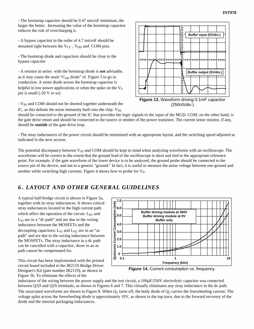
- The bootstrap capacitor should be 0.47 microF minimum, thelarger the better. Increasing the value of the bootstrap capacitorreduces the risk of overcharging it.
- A bypass capacitor in the order of 4.7 microF should bemounted right between the VCC , VDD and COM pins.
- The bootstrap diode and capacitors should be close to thebypass capacitor
- A resistor in series with the bootstrap diode is not advisable,as it may cause the main “Csub diode” of Figure 3 to go inconduction. A zener diode across the bootstrap capacitor ishelpful in low power applications or when the spike on the VS
pin is small (-20 V or so)
- VSS and COM should not be shorted together underneath the
IC, as this defeats the noise immunity built into the chip. VSS
should be connected to the ground of the IC that provides the logic signals to the input of the MGD. COM, on the other hand, isthe gate drive return and should be connected to the source or emitter of the power transistor. The current sense resistor, if any,should be outside of the gate drive loop.
- The stray inductances of the power circuit should be minimized with an appropriate layout, and the switching speed adjusted asindicated in the next section.
The potential discrepancy between VSS and COM should be kept in mind when analyzing waveforms with an oscilloscope. Thewaveforms will be correct to the extent that the ground lead of the oscilloscope is short and tied to the appropriate referencepoint. For example, if the gate waveform of the lower device is to be analyzed, the ground probe should be connected to thesource pin of the device, and not to a generic "ground." In fact, it is useful to measure the noise voltage between one ground andanother while switching high currents. Figure 4 shows how to probe for VS.
6. LAYOUT AND OTHER GENERAL GUIDELINES
A typical half-bridge circuit is shown in Figure 5a,together with its stray inductances. It shows criticalstray inductances located in the high current pathwhich affect the operation of the circuit. LD1 and
LS2 are in a “dc path” and are due to the wiringinductance between the MOSFETs and thedecoupling capacitors; LS1 and LD2 are in an “acpath” and are due to the wiring inductance betweenthe MOSFETs. The stray inductance in a dc pathcan be cancelled with a capacitor, those in an acpath cannot be compensated for.
This circuit has been implemented with the printedcircuit board included in the IR2110 Bridge DriverDesigner's Kit (part number IR2119), as shown inFigure 5b. To eliminate the effects of theinductance of the wiring between the power supply and the test circuit, a 100µF/250V electrolytic capacitor was connectedbetween Q1D and Q2S terminals, as shown in Figures 6 and 7. This virtually eliminates any stray inductance in the dc path.The associated waveforms are shown in Figure 8. When Q1 turns off, the body diode of Q2 carries the freewheeling current. Thevoltage spike across the freewheeling diode is approximately 10V, as shown in the top trace, due to the forward recovery of thediode and the internal packaging inductances.
Buffer driving module at 400VBuffer driving module at 0V
Buffer only
7.0
6.0
5.0
4.0
3.0
2.0
1.0
00.1 1 10
Frequency (kHz)
Qui
esce
nt C
urre
nt C
onsu
mpt
ion
(mA
)
Figure 14. Current consumption vs. frequency
INT978
However, the correspondingnegative spike at pin 5 of theIR2110 is 50V, as shown by thelower trace. This is caused by thedi/dt in the stray inductances LD2
and LS2 in the ac path and thefact that these inductanceseffectively isolate pin 5 from theclamping action of thefreewheeling diode. The severityof the problem can be understoodconsidering that by switching10A in 20ns with a strayinductance of 50nH, a 25V spikeis generated. A small paper cliphas an inductance of 50 nH.The most effective way of dealingwith this spike is to reduce thestray inductance in the ac path.This can be done by mounting thesource or emitter of the high-sidedevice very close to the drain orcollector of the low-side device,as shown in the layout of Figure10.
After this inductance has been reduced to the lowestpractical limit, the di/dt may have to be reduced byreducing the switching speed by means of the gateresistor. Driving MOS-gated power transistorsdirectly from the IR2110 or similar MGD can resultin unnecessarily high switching speeds. The circuitshown in figure 5b produced 4ns turn-off time with0Ω series gate resistance and generated a negativespike of 90V at pin 5 of the IR2110. A graph of thenegative spike and the turn-off time versus seriesgate resistance is shown in Figure 9.
Increasing the value of the series gate resistor, theamplitude of the negative spike decreases rapidly,while the turn-off time is a linear function of theseries gate resistance. Selecting a resistor value justright from the "knee" in Figure 9 provides a goodtrade-off between the spike amplitude and the turn-off speed. A 27Ω speed gate resistor was selected forthe test circuit which resulted in an 18V spikeamplitude and set the turn-off time to 48ns. Aparallel diode, with the anode towards the gate,across the gate resistor is also recommended. Thediode is reverse biased at turn-on but holds the gatedown at turn-off, and during the off state. Thereduction in the turn-on speed reduces the spike of reverse recovery, as explained in Section 12 (see also Ref 2). The value ofgate resistor should be as low as the layout allows, in terms of overvoltage on the device and negative spikes on the VS pin.
The layout should also minimize the stray inductance in the charge/discharge loops of the gate drive to reduce oscillations and toimprove switching speed and noise immunity, particularly the "dv/dt induced turn-on". To this end, each MOSFET should havea dedicated connection going directly to the pin of the MGD for the return of the gate drive signal. Best results are obtained witha twisted pair connected, on one side, to gate and source, on the other side, to gate drive and gate drive return.
Figure 15. Application circuit schematic
+15V
9VDD VB
6
HO7
VS
IR2110
VCC
LO
COMVSS
LIN
SD
HIN10
11
12
13
5
3
1
2
+100µµF
HIN
LIN
SD
15VRTN
0.1µµF
0.1µµF
IRFD9110
IRFD110
IRFD9110
100
IRFD110
100
IRFD9110
+10µµF
IRFD110
+10µµF
IRFD9110
IRFD110
IGBTMODULE(S)
IGBTMODULE(S)
HVRTN
TOLOAD
CF+
HV
Figure 16. High-side drive provides fast switching,continuous on-tome and protection for the switching device.
VCC
1N
ERR
VSS
VB
DUT
CS
VS
1
2
3
4 5
6
7
8+
1µµF+12V
IN
ERR
12VRTN
100pF
IR2125
11DF6
100nF
RG
+HV
RS
10nF100K
ICM755
2
6
1nF
TRIG
THR
OUT
RES
V+GND
3
4
8100nF
IN4148
IN4148
15V
100K 1W
HV RTN
LOAD
INT978
On PC boards parallel tracks should be used. The layout shown in Figure 10 is reduces the stray inductances in the ac path, inthe dc path, as well as the stray inductance in the gate drive loop. In this circuit the voltage differential measured between thegate pin of the power MOSFET and the drive pin of the IR2110 during a fast transient was in excess of 2V.
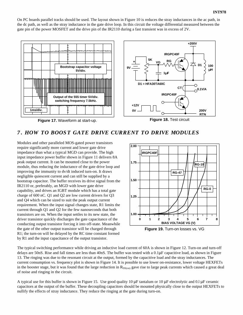
7. HOW TO BOOST GATE DRIVE CURRENT TO DRIVE MODULES
Modules and other paralleled MOS-gated power transistorsrequire significantly more current and lower gate driveimpedance than what a typical MGD can provide. The highinput impedance power buffer shown in Figure 11 delivers 8Apeak output current. It can be mounted close to the powermodule, thus reducing the inductance of the gate drive loop andimproving the immunity to dv/dt induced turn-on. It drawsnegligible quiescent current and can still be supplied by abootstrap capacitor. The buffer receives its drive signal from theIR2110 or, preferably, an MGD with lower gate drivecapability, and drives an IGBT module which has a total gatecharge of 600 nC. Q1 and Q2 are low current drivers for Q3and Q4 which can be sized to suit the peak output currentrequirement. When the input signal changes state, R1 limits thecurrent through Q1 and Q2 for the few nanoseconds that bothtransistors are on. When the input settles to its new state, thedriver transistor quickly discharges the gate capacitance of theconducting output transistor forcing it into off-state. Meanwhilethe gate of the other output transistor will be charged throughR1; the turn-on will be delayed by the RC time constant formedby R1 and the input capacitance of the output transistor.
The typical switching performance while driving an inductive load current of 60A is shown in Figure 12. Turn-on and turn-offdelays are 50nS. Rise and fall times are less than 40nS. The buffer was tested with a 0.1µF capacitive load, as shown in Figure13. The ringing was due to the resonant circuit at the output, formed by the capacitive load and the stray inductances. Thecurrent consumption vs. frequency plot is shown in Figure 14. It is possible to use lower on-resistance, lower voltage HEXFETsin the booster stage, but it was found that the large reduction in RDS(on) gave rise to large peak currents which caused a great dealof noise and ringing in the circuit.
A typical use for this buffer is shown in Figure 15. Use good quality 10 µF tantalum or 10 µF electrolytic and 0.l µF ceramiccapacitors at the output of the buffer. These decoupling capacitors should be mounted physically close to the output HEXFETs tonullify the effects of stray inductance. They reduce the ringing at the gate during turn-on.
Figure 17. Waveform at start-up.
Bootstrap capacitor voltage5V/div.
Output of the 555 timer 5V/div.switching frequency 7.5kHz.
1ms/div.
Figure 18. Test circuit
+200V
100µµH
D1
0.1V/A
200VRTN
CT
IRGPC40F
IRGPC40F
RG
+12V
0V
1µµF
VG5K
D1 = HFA30TA60C
+
9V
Figure 19. Turn-on losses vs. VG
IRGPC40F
RG-47
RG-0
RG-10
2.00
1.75
1.50
1.00
1.25
0 1 2 3 4 5 6 7 8BIAS VOLTAGE VG (V)
INT978
Use short, tightly twisted wires between the output of the buffers and the modules. Use a single point ground at the emitter of thebottom IGBT module. In a bridge configuration, connect the emitters of the bottom IGBT modules to a common point with shortheavy wires. Use this point as a common ground.
8. HOW TO PROVIDE A CONTINUOUS GATE DRIVE
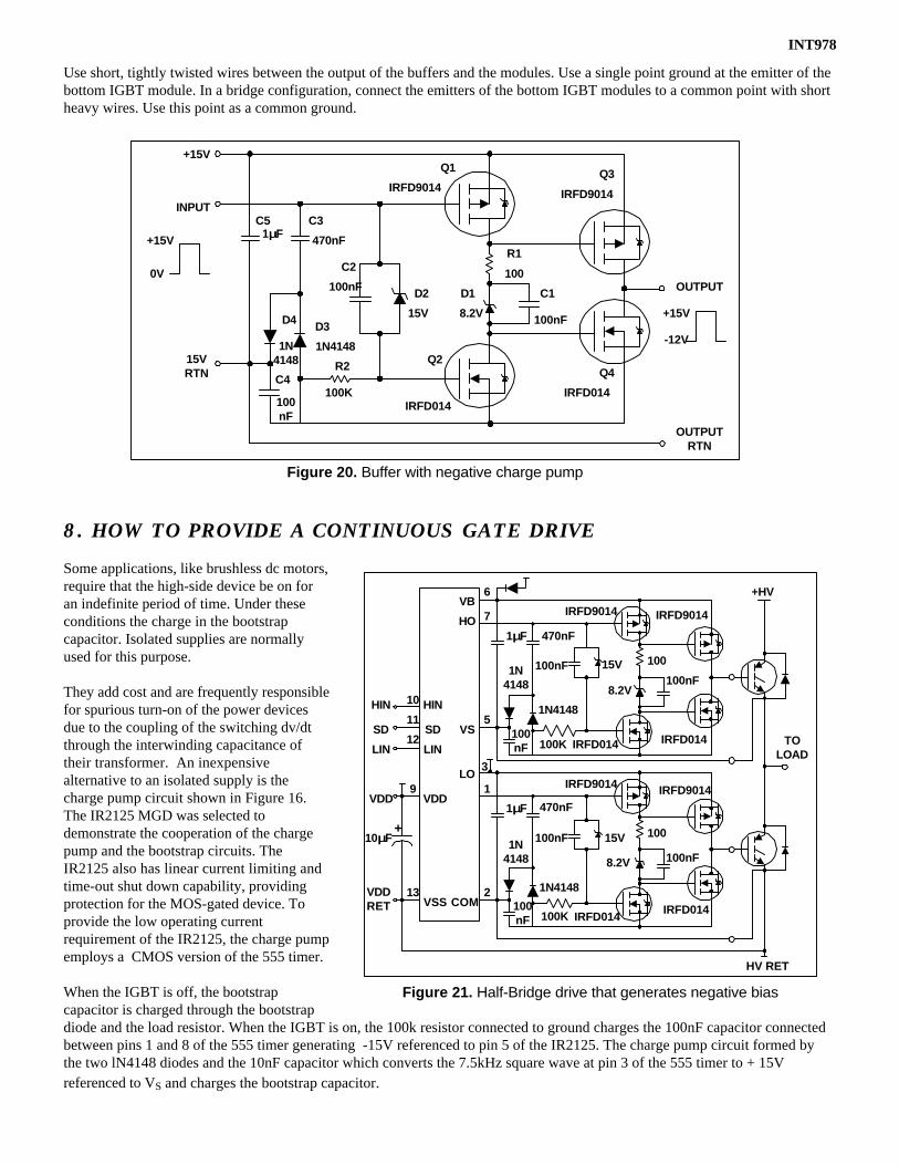
Some applications, like brushless dc motors,require that the high-side device be on foran indefinite period of time. Under theseconditions the charge in the bootstrapcapacitor. Isolated supplies are normallyused for this purpose.
They add cost and are frequently responsiblefor spurious turn-on of the power devicesdue to the coupling of the switching dv/dtthrough the interwinding capacitance oftheir transformer. An inexpensivealternative to an isolated supply is thecharge pump circuit shown in Figure 16.The IR2125 MGD was selected todemonstrate the cooperation of the chargepump and the bootstrap circuits. TheIR2125 also has linear current limiting andtime-out shut down capability, providingprotection for the MOS-gated device. Toprovide the low operating currentrequirement of the IR2125, the charge pumpemploys a CMOS version of the 555 timer.
When the IGBT is off, the bootstrapcapacitor is charged through the bootstrapdiode and the load resistor. When the IGBT is on, the 100k resistor connected to ground charges the 100nF capacitor connectedbetween pins 1 and 8 of the 555 timer generating -15V referenced to pin 5 of the IR2125. The charge pump circuit formed bythe two lN4148 diodes and the 10nF capacitor which converts the 7.5kHz square wave at pin 3 of the 555 timer to + 15Vreferenced to VS and charges the bootstrap capacitor.
Q1
IRFD9014Q3
IRFD9014
OUTPUT
+15V
-12V
OUTPUTRTN
Q4
IRFD014
Q2
IRFD014
C1
100nF
R1
100
D1
8.2V
D2
15V
C2
100nF
1N4148
D3D4
1N4148
C4
100nF
R2
100K
C3
470nF
C51µµF
15VRTN
INPUT
+15V
+15V
0V
Figure 20. Buffer with negative charge pump
Figure 21. Half-Bridge drive that generates negative bias
TOLOAD
+HV
HV RET
IRFD014IRFD014
100nF
100
8.2V
15V100nF
IRFD9014IRFD9014
100K100nF
1N4148
1N4148
470nF1µµF
IRFD9014IRFD9014
100
100nF
IRFD014IRFD014100K100nF
1N4148
1N4148
100nF
470nF1µµF
15V
8.2V
VB
HO
VS
LO
COMVSS
VDD
LIN
SD
HINHIN
SD
LIN
VDD
VDDRET
10µµF+
6
7
5
3
1
213
9
12
11
10
INT978
Figure 17 shows the circuit waveforms at start-up. As the IGBT turns on, the bootstrap diode disconnects pin 8 of the IR2125from the +12V power supply, and the voltage across the bootstrap capacitor starts dropping. At the same time the 100k resistorlocated between pin 1 of the 555 timer and ground starts charging the 100nF capacitor connected to it and generates supplyvoltage for the CMOS (MAXIM ICL71555IPA) timer.
The output voltage of the charge pump increases with increasingsupply voltage. The charge pump maintains the voltage in thebootstrap capacitor, keeping the voltage above the undervoltagethreshold level of the IR2125.
The following considerations should be kept in mind in the selectionof the components:
- In selecting the zener, consider that he absolute maximum voltagesupply voltage for the 555 is 18V
- The 100k lW resistor should be sized according to the maximumsupply current at the high side of the IR2125, the minimumoperating power supply voltage and the timing requirements
- The supply current at the VB pin (IQBS) of the IR2125 increaseswith increasing temperature
9. HOW TO GENERATE A NEGATIVE GATE BIAS
Inherently neither the MOSFET nor the IGBT requires negative bias on the gate. Setting the gate voltage to zero at turn-offinsures proper operation and virtually provides negative bias relative to the threshold voltage of the device. However, there arecircumstances when a negative gate drive is necessary:
• The semiconductor manufacturer specifies negative gate bias for the device,• When the gate voltage can not be held safely below the threshold voltage due to noise generated in the circuit.• The ultimate in switching speed is desired
Although reference will be made to IGBTs, theinformation contained is equally applicable to powerMOSFETs. The IGBTs made by International Rectifier donot require negative bias. The switching times and energyloss values that are published on the data sheets for bothdiscretes and modules were measured at zero gate voltageturn-off. The problem of “dv/dt induced turn-on” ariseswhen the voltage increases rapidly between the collector-emitter terminals of the IGBT.
During the transient, the gate-collector (Miller)capacitance delivers charge to the gate, increasing the gatevoltage. The height and width of the voltage 'blip' at thegate is determined by the ratio of the gate- collector andgate-emitter capacitances, the impedance of the drivecircuit connected to the gate, and the applied dv/dtbetween the collector-emitter terminals.
The following test was conducted to determine thethreshold voltage and the effect of the series gate resistancein high dv/dt applications. The test circuit is shown inFigure 18. The positive bias to the upper IGBT was increased until the switching losses in the bottom IGBT indicated excessiveshoot-through current. The turn-on loss was measured at 15A inductor current and 6V/ns switching speed. The results areshown in Figure 19.
Figure 22. Waveform from negative biasHalf-Bridge driver (1ms/div.)
Input to Buffer10V/div.
IGBT Gate10V/div.
CollectorCurrent10A/div.
Figure 23. Half-Bridge driver with external negative bias
Q1VB
HO
VS
VCC
LO
COM
VSS
LIN
SD
HIN
VDD
+HV
IRGPC50U
IRGPC50UQ2
HVRET
V1
4.7V
100K
-5V
6
7
5
3
1
2
13
12
11
10
9 1µµF
0.47µµF
0.47µµF
100nF
10µµF
++12V
HIN
SD
LIN
12V RTN5V RTN
TOLOAD
IR2110
10KF60
-5V
V1
INT978
The threshold voltage levels increasing the turn-on losses are 4V, 5V and 5.6V with 47Ω, 10Ω, and 0Ω series gate resistance,respectively. A parallel diode across the series gate resistor (anode toward the gate) helps clamp the gate low, so the series gateresistor can be sized according to the turn-on requirements. The current 'blip' due to charging the output capacitance (Coes) ofthe IGBT is frequently mistaken for conduction current. The amplitude of the current 'blip' is approximately 5A for a IRGPC50FIGBT at a dv/dt of 20V/ns. The amplitude of the 'blip' does not change with the applied negative bias.
The basic buffer circuit and the negative chargepump are shown in Figure 20. The buffer circuitemploys two p-channel and two n-channelMOSFETs. Resistor R1 between the gates of Q3and Q4 slows down the turn-on of the outputtransistor and limits the shoot-through current inthe drivers.
D1 reduces the voltage to the gate of Q3 and Q4.D2, C2 and R2 form a level shifter for Q2. C3,C4, D3 and D4 convert the incoming signal tonegative DC voltage. After turn-on, the negativevoltage settles in a few cycles even at extremelylow or high duty cycles (1-99%). The settlingtime and the stiffness of the negative voltage areaffected by the output impedance of the signalsource.
IN
VCC
ERR
VSS
VB
OUT
CS
VS
6
7
1
2
3
4
10K
C1+ 15V D1 14.3V+
VCC
15V
FROMPWM
RG
VB - VS = 2.3V
CB12V
Q1
D2+
C0
V0 +12V
VINCIN+
L1
+
+
Figure 26. In battery charger applications, the +12V from the output appears at the VS pin and reducesthe voltage across CB at start-up and the undervoltage protection in the IR21XX inhibits the operation.
Figure 24. Waveform from circuitshown in Figure 23 (2ms/div)
Input to IR21105V/div.
IGBT Gate5V/div.
Figure 25. Buck Converter
IRF450
VR < 500V
POWER GROUND
LOA
D
C8
7
6
54
3
2
1VB
HO
VSCOM
HIN
VCC
D1
+15
1µµF
LOGIC GROUNDD1: 1N6622, UF4005C: 0.47mF ( f > 5kHz FOR IRF540 OR SIMILAR DIE SIZES)
Figure 27. Adding R1 to the circuit, charging current can bederivated from VIN.
R1 Q1
RG
CB
D2 C0
V0IL
LOAD
L1
CIN VIN+ +
1 mA AVERAGED1
D36
7
1QBS=0.8mA
+15V
IR2125
VB
OUT
CS
VS
INT978
The circuit shown in Figure 21 utilizesthe high voltage level shifting capabilityof the IR2110 combined with the drivecapability and negative bias of the MOSbuffer shown in Figure 20. The circuitwas tested with two 270 A IGBTmodules with 600 nC of gate charge.The waveforms are shown in Figure 22.The turn-on delay of the circuit is 1 µS,the turn-off delay is 0.2 µS .
The settling time of the negative biasvoltage is about 10ms at 5kHz switchingfrequency at 50% duty cycle. At start-up, the circuit delivers some negativegate voltage even after the first cycle.During power down, the gate voltageremains negative until the reservoircapacitor discharges. A simpler circuitis shown in Figure 23. Input and outputwaveforms are shown in Figure 24. Thenegative voltage is provided by an
external power supply, while the negative bias voltage for the high-side is generated by a 100k resistor and a zener diode. Thenegative gate voltages are limited to the maximum applicable offset voltage between the VSS-COM and VSS-VS pins. The totalpower supply voltage to the IR2110 cannot exceed 20V. The 100k resistor is sufficient for HV=160V, 50% duty cycle operation.Different operating conditions may require different resistor values. The average current through the resistor should be at least1mA. The power handling capability and maximum operating voltage of the resistor also have to be considered. Since theoperating current of the zener diode is small, the special low current ones are preferable in this application.
10. HOW TO DRIVE A BUCK CONVERTER
Figure 25 shows a typical implementation of a buck converter with the high side drive function performed by the IR2117. Thediode connected on COM prevents the negative spikes from affecting the operation of the IC and provides an extra measure ofnoise immunity. As mentioned before, COM should not be connected together.
At start-up the bootstrap capacitor is discharged and, in most applications would charge through the inductor and the filtercapacitor. The same is true under no-load conditions, when the freewheeling diode may not conduct at all. This alternative pathworks, as long as the filter capacitor is at least 10 times larger than the bootstrap capacitor. The Q of this resonant circuit shouldbe low enough to insure that the bootstrap capacitor does not get charged beyond the limits of VSS (20V). If this is not so, azener in parallel with the bootstrap capacitor would take care of possible overvoltages. This is true whether the dc-to-dcconverter performs the function of a supply or speed control for a dc motor.
In the following two cases, however, the recharging current for the bootstrap capacitor cannot flow neither in the diode, nor inthe load:
1. In a typical battery charger applications, as the one shown in Figure 26, the +12V from the output appears at the VS pin andreduces the voltage across bootstrap capacitor at start-up and the undervoltage protection in the MGD inhibits the operation.
2. When the regular PWM operation of the buck is interrupted due excessive voltage at the output. This is normally due to a
sudden removal of a heavy load at the output which results in higher output voltage than the set value due to the limitedspeed of the control loop and the stored energy in the Ll inductor. With no load or light load at the output, the filtercapacitor can keep the output high for long time while the CB is being discharged at faster rate by the leakage current of thehigh-side driver.
Figure 28. Dual forward converter and switched reluctance motors
As shown in Figure 27, theaddition of R1 provides analternative charging path forthe bootstrap capacitor.Because VIN is higher thanVO, some charging currentalways flows through R1even if VS pin is sitting at
VO potential.
To keep CB charged theaverage current through R1should be higher than theworst case leakage current.D3 should be a low levelzener diode with sharp kneeat low currents. Therecommended part numbersfor 12V and 15V arerespectively: lN4110 andlN4107.
This technique can also be used in place of a dedicated supply to power the PWM controller, as well as the IR2110 and otherauxilliary circuits, if the output voltage of the buck converter is between 10 and 20V.
Figure 28 shows a bridge arrangementthat is frequently used to drive thewindings of a switched reluctance motoror a transformer in a dual forwardconverter.
L1 L1VR
CURRENTSENSING
9
10
12
11
13
SDVSS
LIN
HIN
VDD
.47µµF
LO
VS
6
7
5
3
1
2
VBD1
C1
2.2µµFVCC
HO
COM
L2
9
10
12
11
13
SDVSS
LIN
HIN
VDD
.47µµF
LO
VS
6
7
5
3
1
2
VBD1
C1
2.2µµFVCC
HO
COM
L2
Figure 29. Typical implementation of all H-Bridge with cycle-by-cycle current mode control
9
10
12
11SD
VSS
LIN
HIN
VDD
.47µµF
LO
VS
6
7
5
3
1
2
VB
+15V
0.47µµF
22
22
COM
13
+15V
HO
VCC
11DF4
1N4148
1N4148
50µµF
100µµF
50µµF
+160V
IR2110
Figure 30a. Test circuit for waveforms shown in Figure 30b. IRF450 operated atapproximately 100kHz in a 100 mH inductor.
Figure 30b.
VDS OF HIGH SIDE IRF45050V/div.
VBS 5V/div. (AC)
Vgs OF HIGH SIDE IRF450
5V/div.
2µµs/div. (93kHz)
INT978
The use of the IR2110 requires the addition of four to insure that the bootstrap capacitor is charged at turn on and in subsequentcycles, should the conduction time of the freewheeling diodes become very short.
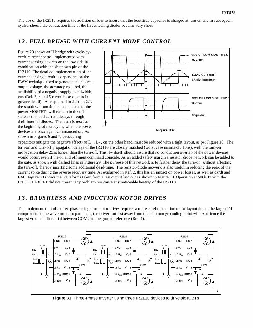
12. FULL BRIDGE WITH CURRENT MODE CONTROL
Figure 29 shows an H bridge with cycle-by-cycle current control implemented withcurrent sensing devices on the low side incombination with the shutdown pin of theIR2110. The detailed implementation of thecurrent sensing circuit is dependent on thePWM technique used to generate the desiredoutput voltage, the accuracy required, theavailability of a negative supply, bandwidth,etc. (Ref. 3, 4 and 5 cover these aspects ingreater detail). As explained in Section 2.1,the shutdown function is latched so that thepower MOSFETs will remain in the off-state as the load current decays throughtheir internal diodes. The latch is reset atthe beginning of next cycle, when the powerdevices are once again commanded on. Asshown in Figures 6 and 7, decouplingcapacitors mitigate the negative effects of Ll . L2 , on the other hand, must be reduced with a tight layout, as per Figure 10. Theturn-on and turn-off propagation delays of the IR2110 are closely matched (worst case mismatch: 10ns), with the turn-onpropagation delay 25ns longer than the turn-off. This, by itself, should insure that no conduction overlap of the power deviceswould occur, even if the on and off input command coincide. As an added safety margin a resistor diode network can be added tothe gate, as shown with dashed lines in Figure 29. The purpose of this network is to further delay the turn-on, without affectingthe turn-off, thereby inserting some additional dead-time. The resistor-diode network is also useful in reducing the peak of thecurrent spike during the reverse recovery time. As explained in Ref. 2, this has an impact on power losses, as well as dv/dt andEMI. Figure 30 shows the waveforms taken from a test circuit laid out as shown in Figure 10. Operation at 500kHz with theIRF830 HEXFET did not present any problem nor cause any noticeable heating of the IR2110.
13. BRUSHLESS AND INDUCTION MOTOR DRIVES
The implementation of a three-phase bridge for motor drives requires a more careful attention to the layout due to the large di/dtcomponents in the waveforms. In particular, the driver furthest away from the common grounding point will experience thelargest voltage differential between COM and the ground reference (Ref. 1).
VDS OF LOW SIDE IRF830
50V/div.
LOAD CURRENT
1A/div. into 50 µµH
VGS OF LOW SIDE IRF830
10V/div.
0.5µµs/div.
Figure 30c.
Figure 31. Three-Phase Inverter using three IR2110 devices to drive six IGBTs
7
6
5
4
3
2
1
8
9
10
11
12
13
14
HO
VB
VS
NC
VCC
COM
LONC
VSS
LIN
SD
HIN
VDD
NC
IR2110
+15V
15V
0V
15V
0V+15V
φφ1
7
6
5
4
3
2
1
8
9
10
11
12
13
14
HO
VB
VS
NC
VCC
COM
LONC
VSS
LIN
SD
HIN
VDD
NC
IR2110
+15V
15V
0V
15V
0V+15V
φφ2
7
6
5
4
3
2
1
8
9
10
11
12
13
14
HO
VB
VS
NC
VCC
COM
LONC
VSS
LIN
SD
HIN
VDD
NC
IR2110
+15V
15V
0V
15V
0V+15V
φφ3
INT978
In the case of the three-phase drivers, likethe IR213x, the guidelines of Sections 5 and6 should be complemented with thefollowing: Three separate connectionsshould go from the COM pin of the MGD tothe three low-side devices. Furthermore,there are several operating conditions thatrequire close scrutiny as potential problemareas.
One such condition could occur when abrushless dc motor is operated with lockedrotor for an indefinite period of time withone leg of the bridge being off.In this condition the bootstrap capacitorcould eventually discharge, depending onthe voltage seen by VS during this period oftime. As a result the top power device would shut off and would not go on when commanded to do so. In most cases this wouldnot be a cause for malfunction, since the lower device would be commanded on next and the bootstrap capacitor would becharged and ready for next cycle. In general, if the design cannot tolerate this type of operation, it can be avoided in one of fourways:
a. a charge pump could be implemented, as described in Section 8; b. the control could be arranged to have a very short "normal" duty cycle with a minimum pulse width of a couple of
microseconds; c. if a pole can be inactive for a limited and known period of time, the bootstrap capacitor could be sized to hold up the charge
for that time. d. Isolated supplies could be provided for the high-side, in addition to the bootstrap capacitor.
If the bridge is part of an induction motordrive that use a PWM technique tosynthesize a sine wave, each pole goesthrough prolonged periods of time with zeroor very low duty cycle at low frequency. Thebootstrap capacitor should be sized to holdenough charge to go through these periodsof time without refreshing. In circuits likethe one shown in Figure 31, galvanicisolation between the high voltage supplyand the logic circuitry is frequentlymandated by safety considerations ordesirable as a form of damage containmentin case of inverter failure.
Optoisolators or pulse transformers arefrequently used to perform this function. Fordrives up to 5 kW, the circuit shown in INT-985 is probably the simplest and most cost-effective way of providing isolation. The useof an MGD shields the optoisolator from thehigh-voltage dv/dt and reduces their costwhile providing a high performance gatedrive capability.
6
7
5
3
2
1
9
10
11
12
13
HO
VB
VS
VCC
COM
LO
VSS
LIN
SD
HIN
VDD
IR2112
Rg
1µµF
1µµF
Rg
+Vdc+12V
LogicSupply
LogicInput
Figure 32. Push Pull Drive Circuit
7
6
5
3
1
2
9
10
11
12
13
IR2110
VDD
HIN
SD
LIN
VSS
VB
VS
VCC
LOAD
Figure 33. IR2110 driving a high side P-Channel
INT978
14. PUSH-PULL
High-voltage MGDs can still make a very useful contribution in applications that do not capitalize on their key feature, the highvoltage level shifting and floating gate drive.
Convenience, noise resilience between VSS and COM and high speed drive capability are appealing features in most powerconditioning applications. They can perform the interface and gate drive function with the simple addition of the decouplingcapacitors, as shown in Figure 32.
15. HIGH-SIDE P-CHANNEL
MGDs can also drive a P-Channel device as a high side switch, provided that a negative supply referenced to the positive rail isavailable, as shown in Figure 33. When operated in this mode, the HIN input becomes active low, i.e. a logic 0 at the input turnson the PChannel MOSFET. Whenever VS (or VB) are at fixed potential with respect to ground, the power losses mentioned inSection 4.2.d.2 would be zero.
16. THYRISTOR GATE DRIVE
The circuit shown in Figure 34 can provide isolated gate drive to a thyristor, with status feedback. The 2:1 ratio in the gate drivetransformer doubles the current available to the gate from what is delivered by the MGD.
17. TROUBLESHOOTING GUIDELINES
To analyze the waveforms of the floating channel of the IR2110 a differential input oscilloscope is required. It is assumed thatany voltage differential not referenced to ground is measured in this way.
It is also assumed that obvious checks have been made, for example:
27k 0.1µµF
27k2.7M2.7M
27kCONT
10-15Vdc
47k
22pF
9
10
11
12
13
VDD
HIN
SD
LIN
VSS LO
COM
VCC
VS
VB
HO7
6
5
3
2
1
COM
470
10ohm
10ohm
10ohm
1ohm
0.047µµF
240 ohm0.5 watt
Gate
Cathode
Figure 34. Isolated SCR Gate Drive Circuit
INT978
• Pins are correctly connected and power supplies are decoupled.• The bootstrap charging diode is ultra-fast, rated for the rail voltage.• The shutdown pin is grounded.• Logic inputs do not cause simultaneous conduction of devices, unless the topology requires it.
SYMPTOM POSSIBLE CAUSENo gate drive pulses Verify that Vcc is above the UV lockout value
Gate drive pulses on lower channel only Measure voltage across bootstrap capacitor; it should be abovethe lockout level. If it is not, check why capacitor doesn’t getcharged. Insure that capacitor is charged at turn-on
Erratic operation of top channel Verify that VS doesn't go below COM by more than 5-10V.Verify that high side channel does not go in UV lockout.Verify that dv/dt on VS with respect to COM does not exceed50V/ns. If so, switching may need slowing down.Verify that logic inputs are noise-free with respect to VSS.Verify that input logic signals are longer than 50ns.
Excessive ringing on gate drive signal Reduce inductance of gate drive loop. Use twisted wires,shorten length. If reduction of loop inductance does not bringringing to acceptable level, add gate resistors.
INT978
TABLE 1METHOD BASIC CIRCUIT KEY FEATURES
FLOATINGGATE DRIVE
SUPPLY
GATEDRIVE
FLOATINGSUPPLY
LEVEL SHIFTEROR
OPTO ISOLATOR
LOADOR
LOW SIDEDEVICE
Full gate control for indefinite periods of time.Cost impact of isolated supply is significant(one required for each high side MOSFET).Level shifting a ground referenced signal can betricky: Level shifter must sustain full voltage, switchfast with minimal propagation delays and low powerconsumption.Opto isolators tend to be relatively expensive, limitedin bandwidth and noise sensitive.
PULSETRANSFORMER
LOADOR
LOW SIDEDEVICE
Simple and cost effective but limited in many respects.Operation over wide duty cycles requires complextechniques.Transformer size increases significantly as frequencydecreases.Significant parasitics create less than ideal operationwith fast switching waveforms.
CHARGEPUMP LOAD
ORLOW SIDE
DEVICE
OSCILLATOR
Can be used to generate an "over-rail" voltagecontrolled by a level shifter or to "pump" the gatewhen MOSFET is turned on.In the first case the problems of a level shifter have tobe tackled.In the second case turn on times tend to be too long forswitching applications.In either case, gate canb e kept on for an indefiniteperiod of time.Inefficiencies in the voltage multiplication circuit mayrequire more than two stages of pumping.
BOOTSTRAP
GATEDRIVE
LEVELSHIFTER
LOADOR
LOW SIDEDEVICE
Simple and inexpensive with some of the limitationsof the pulse transformer: duty cycle and on-time areboth constrained by the need to refresh the bootstrapcapacitor.If the capacitor is charged from a high voltage rail,power dissipation can be significant.Requires level shifter, with its associated difficulties.
CARRIERDRIVE
LOADOR
LOW SIDEDEVICEOSCILLATOR
STOP
Gives full gate control for an indefinite period of timebut is somewhat limited in switching performance.This can be improved with added complexity.
INT978
TABLE IIDie Size Rise Time Fill Time
Typical switching times for different HEXFET die sizes
(Vcc=15V, test circuit as in Figure 9, without gate network)
HEX-2HEX-3HEX-4HEX-5HEX-6
25ns38ns53ns78ns116ns
17ns23ns34ns54ns74ns
References:
1. "New High Voltage Bridge Driver Simplifies PWM Inverter Design," by D. Grant, B. Pelly. PCIM Conference 1989 2. Application Note AN-967 "PWM Motor Drive with HEXFET III" 3. Application Note AN-961 "Using HEXSense in Current-Mode Control Power Supplies" 4. Application Note AN-959 "An Introduction to the HEXSense" 5. "Dynamic Performance of Current Sensing Power MOSFETs" by D. Grant and R. Pearce, Electronic Letters, Vol. 24 No.