26
© 2010-2012 HYCON Technology Corp. www.hycontek.com Preliminary DS-HY12P65-V05_EN 1 HY12P65/HY12P66 Datasheet DMM Specialized IC Embedded Digital T-RMS .
© 2010-2012 HYCON Technology Corp. www.hycontek.com
Preliminary DS-HY12P65-V05_EN
1
HY12P65/HY12P66
Datasheet
DMM Specialized IC Embedded Digital T-RMS
.

HY12P65/HY12P66 Digital T-RMS DMM
© 2010-2012 HYCON Technology Corp. www.hycontek.com
Preliminary DS-HY12P65-V05_EN Page 2
2
Table of Contents
1. FEATURES 5
2. BLOCK DIAGRAM 6
2.1 Multi-Function Block.............................................................................................................................. 7
2.2 ADC....................................................................................................................................................... 8
2.3 Power .................................................................................................................................................... 9
3. PACKAGE AND PIN 10
3.1 64PIN Diagram LQFP64 ......................................................................................................................... 10
3.2 Pin Description ........................................................................................................................................ 11
4. REGISTER LIST 15
5. ABSOLUTE MAXIMUM RATINGS 17
5.1 Recommended Operating Conditions ..................................................................................................... 17
5.2 Internal RC Oscillator .............................................................................................................................. 18
5.3 Supply Current into VDD Excluding Peripherals Current ........................................................................ 18
5.4 Port 1~3................................................................................................................................................... 18
5.5 Reset(Brownout, External RST pin, Low Voltage Detect) ....................................................................... 19
5.6 Power System ......................................................................................................................................... 21
5.7 LCD ......................................................................................................................................................... 21
5.8 Σ∆ADC, Power Supply and Recommended Operating Conditions ........................................................ 22
5.9 Σ∆ADC, Temperature Sensor.................................................................................................................. 23
5.10 Analog Input and Switch Performance.................................................................................................. 23
5.11 DMM Comparator .................................................................................................................................. 23
.
HY12P65/HY12P66 Digital T-RMS DMM
© 2010-2012 HYCON Technology Corp. www.hycontek.com
Preliminary DS-HY12P65-V05_EN Page 3
3
6. ORDERING INFORMATION 24
7. PACKAGING INFORMATION 25
8. REVISION RECORD 26
.

HY12P65/HY12P66 Digital T-RMS DMM
© 2010-2012 HYCON Technology Corp. www.hycontek.com
Preliminary DS-HY12P65-V05_EN Page 4
4
Attention:
1. HYCON Technology Corp. reserves the right to change the content of this datasheet without further
notice. For most up-to-date information, please constantly visit our website:
http://www.hycontek.com .
2. HYCON Technology Corp. is not responsible for problems caused by figures or application circuits
narrated herein whose related industrial properties belong to third parties.
3. Specifications of any HYCON Technology Corp. products detailed or contained herein stipulate the
performance, characteristics, and functions of the specified products in the independent state. We
does not guarantee of the performance, characteristics, and functions of the specified products as
placed in the customer’s products or equipment. Constant and sufficient verification and evaluation
is highly advised.
4. Please note the operating conditions of input voltage, output voltage and load current and ensure
the IC internal power consumption does not exceed that of package tolerance. HYCON Technology
Corp. assumes no responsibility for equipment failures that resulted from using products at values
that exceed, even momentarily, rated values listed in products specifications of HYCON products
specified herein.
5. Notwithstanding this product has built-in ESD protection circuit, please do not exert excessive static
electricity to protection circuit.
6. Products specified or contained herein cannot be employed in applications which require extremely
high levels of reliability, such as device or equipment affecting the human body, health/medical
equipments, security systems, or any apparatus installed in aircrafts and other vehicles.
7. Despite the fact that HYCON Technology Corp. endeavors to enhance product quality as well as
reliability in every possible way, failure or malfunction of semiconductor products may happen.
Hence, users are strongly recommended to comply with safety design including redundancy and
fire-precaution equipments to prevent any accidents and fires that may follow.
8. Use of the information described herein for other purposes and/or reproduction or copying without
the permission of HYCON Technology Corp. is strictly prohibited.
.
HY12P65/HY12P66 Digital T-RMS DMM
© 2010-2012 HYCON Technology Corp. www.hycontek.com
Preliminary DS-HY12P65-V05_EN Page 5
5
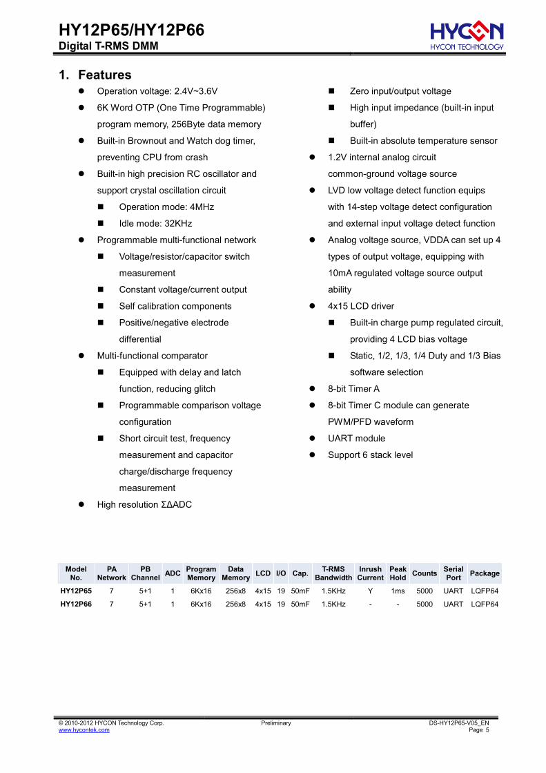
1. Features
Operation voltage: 2.4V~3.6V
6K Word OTP (One Time Programmable)
program memory, 256Byte data memory
Built-in Brownout and Watch dog timer,
preventing CPU from crash
Built-in high precision RC oscillator and
support crystal oscillation circuit
Operation mode: 4MHz
Idle mode: 32KHz
Programmable multi-functional network
Voltage/resistor/capacitor switch
measurement
Constant voltage/current output
Self calibration components
Positive/negative electrode
differential
Multi-functional comparator
Equipped with delay and latch
function, reducing glitch
Programmable comparison voltage
configuration
Short circuit test, frequency
measurement and capacitor
charge/discharge frequency
measurement
High resolution Σ∆ADC
Zero input/output voltage
High input impedance (built-in input
buffer)
Built-in absolute temperature sensor
1.2V internal analog circuit
common-ground voltage source
LVD low voltage detect function equips
with 14-step voltage detect configuration
and external input voltage detect function
Analog voltage source, VDDA can set up 4
types of output voltage, equipping with
10mA regulated voltage source output
ability
4x15 LCD driver
Built-in charge pump regulated circuit,
providing 4 LCD bias voltage
Static, 1/2, 1/3, 1/4 Duty and 1/3 Bias
software selection
8-bit Timer A
8-bit Timer C module can generate
PWM/PFD waveform
UART module
Support 6 stack level
Model
No. PA
Network PB
Channel ADC
Program Memory
Data Memory
LCD I/O Cap.T-RMS
BandwidthInrush
CurrentPeak Hold
Counts Serial Port
Package
HY12P65 7 5+1 1 6Kx16 256x8 4x15 19 50mF 1.5KHz Y 1ms 5000 UART LQFP64
HY12P66 7 5+1 1 6Kx16 256x8 4x15 19 50mF 1.5KHz - - 5000 UART LQFP64
.

HY12P65/HY12P66 Digital T-RMS DMM
© 2010-2012 HYCON Technology Corp www.hycontek.com
Preliminary DS-HY12P65-V05_ENPage 6
2. Block Diagram
Data Memory(STK:6L)
(SP:128B)(GPR:256B)
ProgramMemory
(OTP:6KW)
CPUH08A
HARDWARE MULTIPLIER
8x8
LCD4x15
Watch Dog
RST
XTI XTO VDD VSS PTn.x/BZ
VLCD
SEGx
RCOscillator
(HAO)(LPO)
PAx VDDA ACM
COMx
TMCKI/PPF
Digital TrueRMS&
Digital Filter&
Peak Hold
C C
C
P P
D
D
P
PA P
C C
A Analog PadD Digital PadP Power Pad
TIMERA/C
(PPF)
PORT(PT1、PT2、
PT3、BZ)
Power SystemVoltage Source
(PUMP)(LDO)
RESET(BOR)
(STACK)(WDT)(RST)
ΣΔAD(Switch Network)
(Pre-Filter)(Temp.senor)
Low Voltage Detect(LVD)
VDD
P
Interface(EUART)
C Common I/O Pad
RC
C
TX
C
VGGP
CAP
CBP
P
P
REFO
AGNDCMPO
C
Frequency Counter&
Comparators&
Key Scan
CMPx
A
CNT
S
PBx
A
RLx
A
FTx
A
LVDIN
A
.
HY12P65/HY12P66 Digital T-RMS DMM
© 2010-2012 HYCON Technology Corp www.hycontek.com
Preliminary DS-HY12P65-V05_ENPage 7
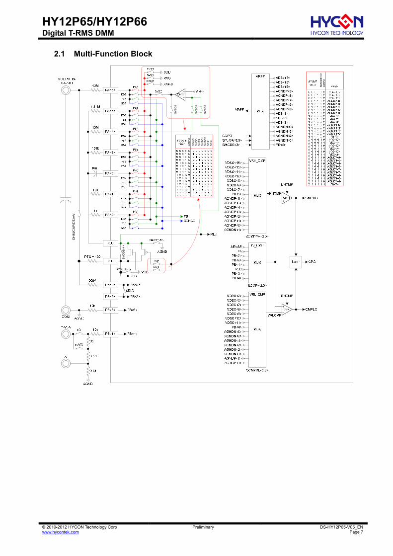
2.1 Multi-Function Block
CM
PO
SM
OD
E<
3>
OH
M/C
AP
/DT
/mV
SM
OD
E<
4>
SV
SO
2
SV
SO
2
SV
SO
2S
GN
DS
VD
DS
VS
SS
VS
O1
SV
SO
2S
CP
SC
N
CM
PO
.
HY12P65/HY12P66 Digital T-RMS DMM
© 2010-2012 HYCON Technology Corp www.hycontek.com
Preliminary DS-HY12P65-V05_ENPage 8
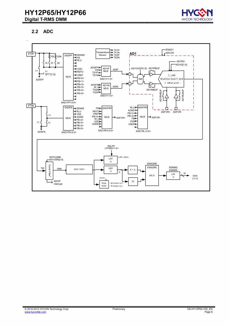
2.2 ADC
AD1IN
AD1IP
SADFP
SADFN
MUXADSFP
SAD1FP<3:0>
SENSEFBRLU
VDDREFO
VREFPB<0>PB<1>PB<2>PB<3>PB<4>
PB<5>
SENSERLUVSSAGNDMUX
SAD1FN<2:0>ADSFN
FBREFOVREF
PB<4>
SADFRP
MUX
SAD1RH<2:0>
ADFVR+
RLUAGNDPB<3>PB<5>
SADFRN
MUX ADFVR-PB<2>PB<3>PB<4>PB<5>
SAD1RL<2:0>
100k10kFTP
FTN
000110
1111
11 11
11
RLUVDD
AGND
FBVSS
VREF
ADSFPFB
TS1PTS1N
MUX
SAD1I<1:0>
ADIP
ADSFNRLU
TS2NTS2P
MUX
SAD1I<1:0>
ADIN
Temperature Sensor
TS1PTS1NTS2PTS2N
AD1IG[1:0]
AD1RG
ΣΔAD
ADFVR+ ADFVR-
ADCCKENAD1
SI:x0.9,x1.8,x2.7, x3.6
+ VR:x1,x1/3 -
AD1
AD
1RH
BU
F
AD
1R
LB
UF
AD1IPBUF
AD1INBUF
INX
AD1CHOP[1:0]
SFT1[1:0]
1bit
Co
mb
Filte
r 2
AD1OSR[2:0]
19bit
ADCIFInterrupt
LPF<18:0>
AD1<18:0> X * X
LPF/n
X
LPFBW<1:0>
HPF/n
LPF/n RMS
[37:0]
38
|X|
MUX
ENSQRE
ENSQRE
RSTCOMB
ENRMS
RSLPF
RSRMS
Peak Hold
ENPKH
PKHMIN<18:0>
PKHMAX<18:0>
.
HY12P65/HY12P66 Digital T-RMS DMM
© 2010-2012 HYCON Technology Corp www.hycontek.com
Preliminary DS-HY12P65-V05_ENPage 9
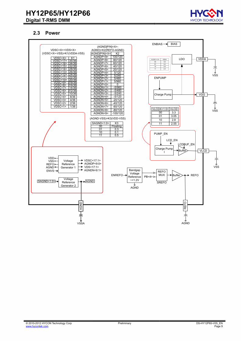
2.3 Power
Voltage Reference
Generator 1
VDSC<17:1>
VDS<17:1>AGNDP<9:0>
AGNDN<9:1>
REFO
RE
FO
AGND
AG
ND
VSSA
AGNDVoltage
Reference Generator 2
SAGND<1:0>
ENVS Bandgap Voltage
Reference~=1.2V
ENREFO
AGND
MUX
SREFO
REFO
PB<4> Buffer
(AGND[P/N]<X>-AGND)=K2(REFO-AGND) VDSC<X>=VDS<X>
(VDSC<X>-VSS)=K1(VDDA-VSS)
VDSC<17>VDSC<16>VDSC<15>VDSC<14>VDSC<13>VDSC<12>VDSC<11>VDSC<10>VDSC<9>VDSC<8>VDSC<7>VDSC<6>VDSC<5>VDSC<4>VDSC<3>VDSC<2>VDSC<1>
35/36
16/3618/3620/3622/3624/3626/3628/3632/3634/36
K1
14/3612/3610/368/364/362/361/36
VDSC<X>
Floating0.30.1
000110
K3SAGND<1:0>
(AGND-VSS)=K3(VDD-VSS)
VDD
REFOAGND
VSS
0.511
ENBIAS BIAS
AGNDP<9>AGNDP<8>AGNDP<7>
100/120
05/9605/4805/2405/120
20/12040/12060/12080/120
K2
-5/960-5/480-5/240-5/120
-20/120-40/120-60/120-80/120-100/120
AGND[P/N]<X>
AGNDP<6>AGNDP<5>AGNDP<4>AGNDP<3>AGNDP<2>AGNDP<1>AGNDP<0>AGNDN<1>AGNDN<2>AGNDN<3>AGNDN<4>AGNDN<5>AGNDN<6>AGNDN<7>AGNDN<8>AGNDN<9> 3.3
3.052.8
000110
VLCDVLCDX<1:0>
2.5511
Charge PumpI Buffer
LCDBUF_EN
VSS
LCD_EN
VLCD
PUMP_EN
Charge Pump
VSS
VGG
ENPUMPVSS
VDDALDO3.6
3.2
2.8
00
01
10
VDDAVLDOC<1:0>
2.411
.

HY12P65/HY12P66 Digital T-RMS DMM
© 2010-2012 HYCON Technology Corp www.hycontek.com
Preliminary DS-HY12P65-V05_ENPage 10
3. Package And Pin 3.1 64PIN Diagram LQFP64
1 2 3 4 5 6 7 8 9 10 11
RST/VPP
12 13 14 15 16
1718
19
202
122
232
425
262
728
29
3031
32
3344 43 42 41 40 39 38 37 36 35 34
VDDA
ACM
VSS
VLCD
COM0
VDD HY12P65/HY12P66LQFP64
48 47 46 45
INT1/PSDI//PT1.1
PT1.2
TST/RC/PT1.3
TX/PT1.4
PSDO/BZ/PT1.7
PT1.6
PT1.5
PF
D/P
WM
/PT
2.2
XT
I/PT
2.1
LVD
IN/T
MC
KI/P
T2
.3
54
5352
51
5049
5857
56
555
96
463
62
6160
SE
G3
SE
G4
SE
G5
SE
G6
SE
G7
SE
G8
SE
G9
SE
G10
SE
G11
SE
G12
SE
G13
XT
O/P
T2.0
SE
G14
INT0/PSCK/PT1.0
CNT/PT3.6
CPMO/PT3.7
INT27/CPM3/PT2.7
INT26/CPM2/PT2.6
INT25/CPM1/PT2.5
INT24/CPM0/PT2.4
PB5/PT3.5
PB4
PB
3
PB
1/P
B2
PB
0
FT
B
FT
N
RLU
RLD
PA
6
PA
5
PA
4
PA
3
PA
2
PA
1
PA
0
RE
FO
AG
ND
VGG
CA
CB
COM1
COM2
COM3
SEG0
SEG1
SEG2
.
HY12P65/HY12P66 Digital T-RMS DMM
© 2010-2012 HYCON Technology Corp www.hycontek.com
Preliminary DS-HY12P65-V05_ENPage 11
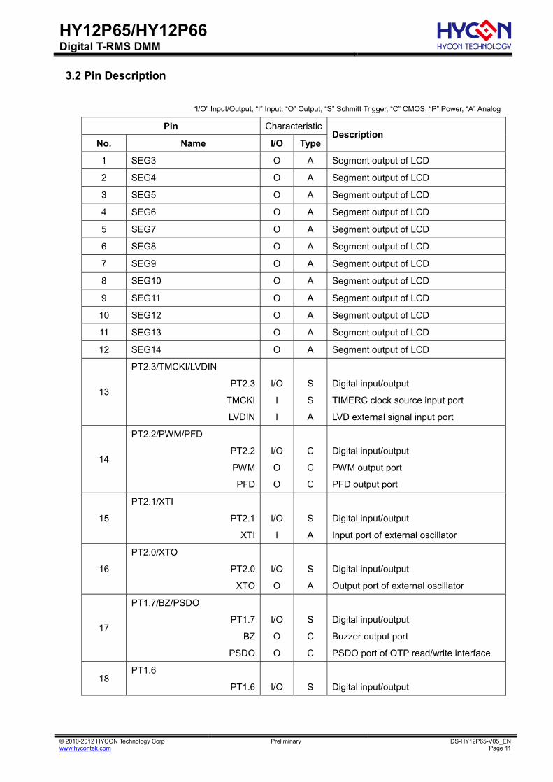
3.2 Pin Description
“I/O” Input/Output, “I” Input, “O” Output, “S” Schmitt Trigger, “C” CMOS, “P” Power, “A” Analog
Pin Characteristic
No. Name I/O TypeDescription
1 SEG3 O A Segment output of LCD
2 SEG4 O A Segment output of LCD
3 SEG5 O A Segment output of LCD
4 SEG6 O A Segment output of LCD
5 SEG7 O A Segment output of LCD
6 SEG8 O A Segment output of LCD
7 SEG9 O A Segment output of LCD
8 SEG10 O A Segment output of LCD
9 SEG11 O A Segment output of LCD
10 SEG12 O A Segment output of LCD
11 SEG13 O A Segment output of LCD
12 SEG14 O A Segment output of LCD
13
PT2.3/TMCKI/LVDIN
PT2.3
TMCKI
LVDIN
I/O
I
I
S
S
A
Digital input/output
TIMERC clock source input port
LVD external signal input port
14
PT2.2/PWM/PFD
PT2.2
PWM
PFD
I/O
O
O
C
C
C
Digital input/output
PWM output port
PFD output port
15
PT2.1/XTI
PT2.1
XTI
I/O
I
S
A
Digital input/output
Input port of external oscillator
16
PT2.0/XTO
PT2.0
XTO
I/O
O
S
A
Digital input/output
Output port of external oscillator
17
PT1.7/BZ/PSDO
PT1.7
BZ
PSDO
I/O
O
O
S
C
C
Digital input/output
Buzzer output port
PSDO port of OTP read/write interface
18 PT1.6
PT1.6
I/O
S
Digital input/output
.
HY12P65/HY12P66 Digital T-RMS DMM
© 2010-2012 HYCON Technology Corp www.hycontek.com
Preliminary DS-HY12P65-V05_ENPage 12
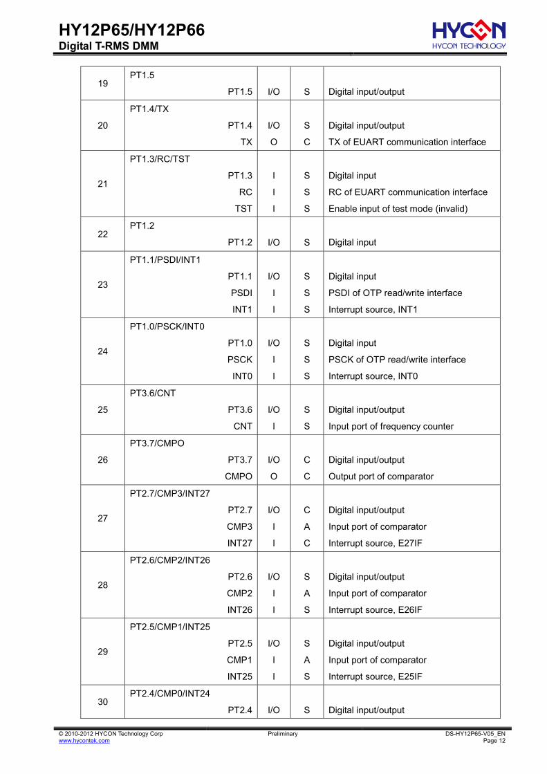
19 PT1.5
PT1.5
I/O
S
Digital input/output
20
PT1.4/TX
PT1.4
TX
I/O
O
S
C
Digital input/output
TX of EUART communication interface
21
PT1.3/RC/TST
PT1.3
RC
TST
I
I
I
S
S
S
Digital input
RC of EUART communication interface
Enable input of test mode (invalid)
22 PT1.2
PT1.2
I/O
S
Digital input
23
PT1.1/PSDI/INT1
PT1.1
PSDI
INT1
I/O
I
I
S
S
S
Digital input
PSDI of OTP read/write interface
Interrupt source, INT1
24
PT1.0/PSCK/INT0
PT1.0
PSCK
INT0
I/O
I
I
S
S
S
Digital input
PSCK of OTP read/write interface
Interrupt source, INT0
25
PT3.6/CNT
PT3.6
CNT
I/O
I
S
S
Digital input/output
Input port of frequency counter
26
PT3.7/CMPO
PT3.7
CMPO
I/O
O
C
C
Digital input/output
Output port of comparator
27
PT2.7/CMP3/INT27
PT2.7
CMP3
INT27
I/O
I
I
C
A
C
Digital input/output
Input port of comparator
Interrupt source, E27IF
28
PT2.6/CMP2/INT26
PT2.6
CMP2
INT26
I/O
I
I
S
A
S
Digital input/output
Input port of comparator
Interrupt source, E26IF
29
PT2.5/CMP1/INT25
PT2.5
CMP1
INT25
I/O
I
I
S
A
S
Digital input/output
Input port of comparator
Interrupt source, E25IF
30 PT2.4/CMP0/INT24
PT2.4
I/O
S
Digital input/output
.
HY12P65/HY12P66 Digital T-RMS DMM
© 2010-2012 HYCON Technology Corp www.hycontek.com
Preliminary DS-HY12P65-V05_ENPage 13
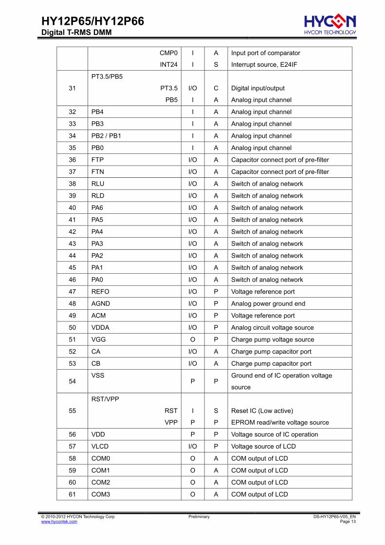
CMP0
INT24
I
I
A
S
Input port of comparator
Interrupt source, E24IF
31
PT3.5/PB5
PT3.5
PB5
I/O
I
C
A
Digital input/output
Analog input channel
32 PB4 I A Analog input channel
33 PB3 I A Analog input channel
34 PB2 / PB1 I A Analog input channel
35 PB0 I A Analog input channel
36 FTP I/O A Capacitor connect port of pre-filter
37 FTN I/O A Capacitor connect port of pre-filter
38 RLU I/O A Switch of analog network
39 RLD I/O A Switch of analog network
40 PA6 I/O A Switch of analog network
41 PA5 I/O A Switch of analog network
42 PA4 I/O A Switch of analog network
43 PA3 I/O A Switch of analog network
44 PA2 I/O A Switch of analog network
45 PA1 I/O A Switch of analog network
46 PA0 I/O A Switch of analog network
47 REFO I/O P Voltage reference port
48 AGND I/O P Analog power ground end
49 ACM I/O P Voltage reference port
50 VDDA I/O P Analog circuit voltage source
51 VGG O P Charge pump voltage source
52 CA I/O A Charge pump capacitor port
53 CB I/O A Charge pump capacitor port
54 VSS
P P Ground end of IC operation voltage
source
55
RST/VPP
RST
VPP
I
P
S
P
Reset IC (Low active)
EPROM read/write voltage source
56 VDD P P Voltage source of IC operation
57 VLCD I/O P Voltage source of LCD
58 COM0 O A COM output of LCD
59 COM1 O A COM output of LCD
60 COM2 O A COM output of LCD
61 COM3 O A COM output of LCD
.

HY12P65/HY12P66 Digital T-RMS DMM
© 2010-2012 HYCON Technology Corp www.hycontek.com
Preliminary DS-HY12P65-V05_ENPage 14
62 SEG0 O A Segment output of LCD
63 SEG1 O A Segment output of LCD
64 SEG2 O A Segment output of LCD
.

HY12P65/HY12P66 Digital T-RMS DMM
© 2010-2012 HYCON Technology Corp www.hycontek.com
Preliminary DS-HY12P65-V05_ENPage 15
4. Register list
Address File Name Bit7 Bit6 Bit5 Bit4 Bit3 Bit2 Bit1 Bit0 A-RESET i-RESET R/W
00H INDF0 N/A N/A *,*,*,* *,*,*,*
01H POINC0 N/A N/A *,*,*,* *,*,*,*
02H PODEC0 N/A N/A *,*,*,* *,*,*,*
03H PRINC0 N/A N/A *,*,*,* *,*,*,*
04H PLUSW0 N/A N/A *,*,*,* *,*,*,*
05H INDF1 N/A N/A *,*,*,* *,*,*,*
06H POINC1 N/A N/A *,*,*,* *,*,*,*
07H PODEC1 N/A N/A *,*,*,* *,*,*,*
08H PRINC1 N/A N/A *,*,*,* *,*,*,*
09H PLUSW1 N/A N/A *,*,*,* *,*,*,*
0FH FSR0H FSR0[8] .... ...x .... ...u -,-,-,- -,-,-,*
10H FSR0L xxxx xxxx uuuu uuuu *,*,*,* *,*,*,*
11H FSR1H FSR1[8] .... ...x .... ...u -,-,-,- -,-,-,*
12H FSR1L xxxx xxxx uuuu uuuu *,*,*,* *,*,*,*
16H TOSH TOS[12] TOS[11] TOS[10] TOS[9] TOS[8] ...0 0000 ...0 0000 -,-,*,* *,*,*,*
17H TOSL 0000 0000 0000 0000 *,*,*,* *,*,*,*
18H STKPTR STKFL STKUN STKOV STKPRT[2] STKPRT[1] STKPRT[0] 000. .000 000. .000 r,rw0,rw0,- -,r,r,r
1AH PCLATH PC[12] PC[11] PC[10] PC[9] PC[8] ...0 0000 ...0 0000 -,-,*,* *,*,*,*
1BH PCLATL 0000 0000 0000 0000 *,*,*,* *,*,*,*
1DH TBLPTRH TBLPTR[12] TBLPTR[11] TBLPTR[10] TBLPTR[9] TBLPTR[8] ...0 0000 ...0 0000 -,-,*,* *,*,*,*
1EH TBLPTRL 0000 0000 0000 0000 *,*,*,* *,*,*,*
1FH TBLDH 0000 0000 0000 0000 *,*,*,* *,*,*,*
20H TBLDL 0000 0000 0000 0000 *,*,*,* *,*,*,*
21H PRODH xxxx xxxx uuuu uuuu r,r,r,r r,r,r,r
22H PRODL xxxx xxxx uuuu uuuu r,r,r,r r,r,r,r
23H INTE1 GIE TMCIE TMAIE WDTIE E1IE E0IE 0.0. 0000 0.0. 0000 *,-,*,- *,*,*,*
24H INTE2 TXIE RCIE RMSIE LPFIE AD1IE SSPIE CTIE 0000 000. 0000 000. *,*,*,* *,*,*,-
25H INTE3 E24IE E25IE E26IE E27IE 0000 …. 0000 …. *,*,*,* -,-,-,-
26H INTF1 TMCIF TMAIF WDTIF E1IF E0IF ..0. 0000 ..0. 0000 -,-,*,- *,*,*,*
27H INTF2 TXIF RCIF RMSIF LPFIF AD1IF SSPIF CTIF 0000 000. 0000 000. *,*,*,* *,*,*,-
28H INTF3 E24IF E25IF E26IF E27IF 0000 …. 0000 …. *,*,*,* -,-,-,-
29H WREG xxxx xxxx uuuu uuuu *,*,*,* *,*,*,*
2AH BSRCN BSR[0] ..... 0000 .... 0000 -,-,-,- *,*,*,*
2BH STATUS C DC N OV Z ...x xxxx ...u uuuu -,-,-,* *,*,*,*
2CH PSTATUS PD TO IDLEB BOR SKERR 000d .0.. uduu .d.. rw0,rw0,rw0,rw0 -,rw0,-,-
2DH LVDCN1 ENLVD LVD VJ1 VJ2
2EH LVDCN2 VSL
2FH SBMSET1 SKRST x.xx xxxx u.uu uuuu *,-,*,* *,*,*,*
30H MCKCN1 HSSEL HSCK ENXT ENHAO 0000 0001 0000 0001 *,*,*,* *,*,*,*
31H MCKCN2 ADCCK PERCK 0000 0000 0000 0000 *,*,*,* *,*,*,*
32H TMACN ENTMA TMACK ENWDT 0000 0000 0000 0000 *,*,*,* w1,*,*,*
33H TMAR xxxx xxxx uuuu uuuu r,r,r,r r,r,r,r
34H TMCCN ENTMC 0000 0000 0000 0000 *,*,*,* *,*,*,*
35H PRC 1111 1111 1111 1111 *,*,*,* *,*,*,*
36H TMCR 0000 0000 0000 0000 r,r,r,r r,r,r,r
37H PWMCN ENPWM ENPFD 0000 0000 0000 0000 *,*,*,* *,*,*,*
38H PWMR xxxx xxxx uuuu uuuu *,*,*,* *,*,*,*
39H LCDCN1 ENLCD LCDPR LCDBF 0000 000. 0000 000. *,*,*,* *,*,*,-
3AH LCDCN2 LCDBL 000. .... 000. .... *,*,*,- -,-,-,-
3BH LCD0 xxxx xxxx uuuu uuuu *,*,*,* *,*,*,*
3CH LCD1 xxxx xxxx uuuu uuuu *,*,*,* *,*,*,*
3DH LCD2 xxxx xxxx uuuu uuuu *,*,*,* *,*,*,*
3EH LCD3 xxxx xxxx uuuu uuuu *,*,*,* *,*,*,*
3FH LCD4 xxxx xxxx uuuu uuuu *,*,*,* *,*,*,*
40H LCD5 xxxx xxxx uuuu uuuu *,*,*,* *,*,*,*
41H LCD6 xxxx xxxx uuuu uuuu *,*,*,* *,*,*,*
42H LCD7 …. xxxx …. uuuu -,-,-,- *,*,*,*''
46H URCON ENSP ENTX TX9 TX9D PARITY WUE 0000 0..0 0000 0..0 *,*,*,* *,-,-,*
47H URSTA RC9D PERR FERR OERR RCIDL TRMT ABDOVF .000 0110 .000 0110 -,r,r,r r,r,r,rw0
48H BAUDCON ENCR RC9 ENADD ENABD .... 0000 .... 0000 -,-,-,- *,*,*,*'
49H BRGRH ...x xxxx ...u uuuu -,-,-,* *,*,*,*
4AH BRGRL xxxx xxxx uuuu uuuu *,*,*,* *,*,*,*
4BH TXREG xxxx xxxx uuuu uuuu *,*,*,* *,*,*,*
4CH RCREG xxxx xxxx uuuu uuuu r,r,r,r r,r,r,r
Baud Rate Generator Register High Byte
Baud Rate Generator Register Low Byte
UART Transmit Register
UART Receive Register
Segment SEG7@[7:4]and SEG6@[3:0] data register of LCD
Segment SEG9@[7:4] and SEG8@[3:0] data register of LCD
Segment SEG11@[7:4] and SEG10@[3:0] data register of LCD
Segment SEG13@[7:4] and SEG12@[3:0] data register of LCD
Segment SEG14@[3:0] data register of LCD
Segment SEG5@[7:4] and SEG4@[3:0] data register of LCD
TMCCK[1:0] TMCS1[2:0]
PWM MSB Byte register
VLCDX[1:0] LCDBI[1:0]
LCDMX[1:0]
PWMRL[1:0]
TMCS0[1:0]
Segment SEG1@[7:4] and SEG0@[3:0] data register of LCD
Segment SEG3@[7:4] and SEG2@[3:0] data register of LCD
HSS[1:0]
TMAS[1:0] WDTS[2:0]
TimerC programmable register
TimerC register
HAOTR[5:0]
TimerA data register
LCDS[2:0] BZS[2:0]
SVIP[3:0]SVIN[2:0]
Contents of FSR0 to address data memory value of FSR0 post-decremented
Contents of FSR0 to address data memory value of FSR0 offset by W
Contents of FSR1 to address data memory value of FSR0 post-decremented
Indirect Data Memory Address Pointer 1 Low Byte,FSR1[7:0]
Top-of-Stack Low Byte (TOS<7:0>)
VLDX[3:0]
Program Memory Table Pointer Low Byte (TBLPTR<7:0>)
“-”no use,“*”read/write,“w”write,“r”read,“r0”only read 0,“r1”only read 1,“w0”only write 0,“w1”omly write 1
“.”unimplemented bit,“x”unknown,“u”unchanged,“d”depends on condition
Contents of FSR0 to address data memory value of FSR0 not changed
Contents of FSR0 to address data memory value of FSR0 post-incremented
Program Memory Table Latch High Byte
Working Register
Contents of FSR0 to address data memory value of FSR0 pre-incremented
Contents of FSR1 to address data memory value of FSR0 pre-incremented
Indirect Data Memory Address Pointer 0 Low Byte,FSR0[7:0]
Contents of FSR1 to address data memory value of FSR0 offset by W
Contents of FSR1 to address data memory value of FSR0 not changed
Contents of FSR1 to address data memory value of FSR0 post-incremented
PC Low Byte for PC<7:0>
Program Memory Table Latch Low Byte
Product Register of Multiply High Byte
Product Register of Multiply Low Byte
CPUCK[1:0]
.
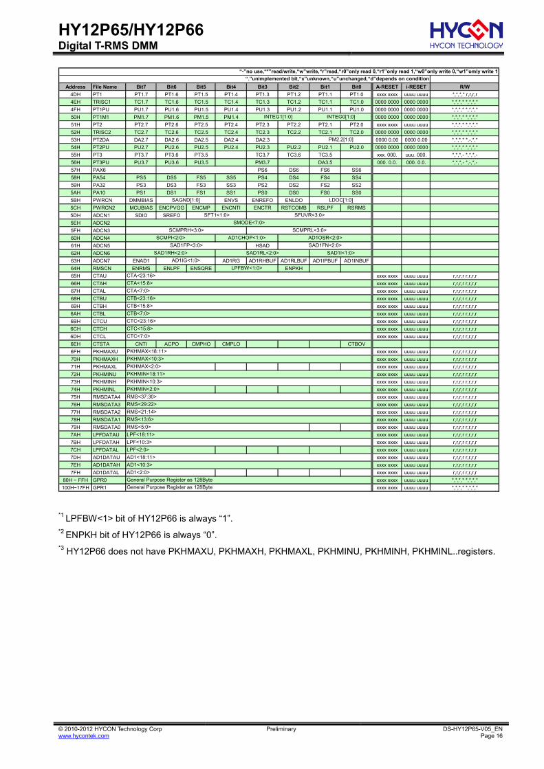
HY12P65/HY12P66 Digital T-RMS DMM
© 2010-2012 HYCON Technology Corp www.hycontek.com
Preliminary DS-HY12P65-V05_ENPage 16
Address File Name Bit7 Bit6 Bit5 Bit4 Bit3 Bit2 Bit1 Bit0 A-RESET i-RESET R/W
4DH PT1 PT1.7 PT1.6 PT1.5 PT1.4 PT1.3 PT1.2 PT1.1 PT1.0 xxxx xxxx uuuu uuuu *,*,*,* r,r,r,r
4EH TRISC1 TC1.7 TC1.6 TC1.5 TC1.4 TC1.3 TC1.2 TC1.1 TC1.0 0000 0000 0000 0000 *,*,*,* *,*,*,*
4FH PT1PU PU1.7 PU1.6 PU1.5 PU1.4 PU1.3 PU1.2 PU1.1 PU1.0 0000 0000 0000 0000 *,*,*,* *,*,*,*
50H PT1M1 PM1.7 PM1.6 PM1.5 PM1.4 0000 0000 0000 0000 *,*,*,* *,*,*,*
51H PT2 PT2.7 PT2.6 PT2.5 PT2.4 PT2.3 PT2.2 PT2.1 PT2.0 xxxx xxxx uuuu uuuu *,*,*,* *,*,*,*
52H TRISC2 TC2.7 TC2.6 TC2.5 TC2.4 TC2.3 TC2.2 TC2.1 TC2.0 0000 0000 0000 0000 *,*,*,* *,*,*,*
53H PT2DA DA2.7 DA2.6 DA2.5 DA2.4 DA2.3 0000 0.00 0000 0.00 *,*,*,* *,-,*,*
54H PT2PU PU2.7 PU2.6 PU2.5 PU2.4 PU2.3 PU2.2 PU2.1 PU2.0 0000 0000 0000 0000 *,*,*,* *,*,*,*
55H PT3 PT3.7 PT3.6 PT3.5 TC3.7 TC3.6 TC3.5 xxx. 000. uuu. 000. *,*,*,- *,*,*,-
56H PT3PU PU3.7 PU3.6 PU3.5 PM3.7 DA3.5 000. 0.0. 000. 0.0. *,*,*,- *,-,*,-
57H PAX6 PS6 DS6 FS6 SS6
58H PA54 PS5 DS5 FS5 SS5 PS4 DS4 FS4 SS4
59H PA32 PS3 DS3 FS3 SS3 PS2 DS2 FS2 SS2
5AH PA10 PS1 DS1 FS1 SS1 PS0 DS0 FS0 SS0
5BH PWRCN DMMBIAS ENVS ENREFO ENLDO
5CH PWRCN2 MCUBIAS ENCPVGG ENCMP ENCNTI ENCTR RSTCOMB RSLPF RSRMS
5DH ADCN1 SDIO SREFO
5EH ADCN2
5FH ADCN3
60H ADCN4
61H ADCN5 HSAD
62H ADCN6
63H ADCN7 ENAD1 AD1RG AD1RHBUF AD1RLBUF AD1IPBUF AD1INBUF
64H RMSCN ENRMS ENLPF ENSQRE ENPKH
65H CTAU xxxx xxxx uuuu uuuu r,r,r,r r,r,r,r
66H CTAH xxxx xxxx uuuu uuuu r,r,r,r r,r,r,r
67H CTAL xxxx xxxx uuuu uuuu r,r,r,r r,r,r,r
68H CTBU xxxx xxxx uuuu uuuu r,r,r,r r,r,r,r
69H CTBH xxxx xxxx uuuu uuuu r,r,r,r r,r,r,r
6AH CTBL xxxx xxxx uuuu uuuu r,r,r,r r,r,r,r
6BH CTCU xxxx xxxx uuuu uuuu r,r,r,r r,r,r,r
6CH CTCH xxxx xxxx uuuu uuuu r,r,r,r r,r,r,r
6DH CTCL xxxx xxxx uuuu uuuu r,r,r,r r,r,r,r
6EH CTSTA CNTI ACPO CMPHO CMPLO CTBOV
6FH PKHMAXU xxxx xxxx uuuu uuuu r,r,r,r r,r,r,r
70H PKHMAXH xxxx xxxx uuuu uuuu r,r,r,r r,r,r,r
71H PKHMAXL xxxx xxxx uuuu uuuu r,r,r,r r,r,r,r
72H PKHMINU xxxx xxxx uuuu uuuu r,r,r,r r,r,r,r
73H PKHMINH xxxx xxxx uuuu uuuu r,r,r,r r,r,r,r
74H PKHMINL xxxx xxxx uuuu uuuu r,r,r,r r,r,r,r
75H RMSDATA4 xxxx xxxx uuuu uuuu r,r,r,r r,r,r,r
76H RMSDATA3 xxxx xxxx uuuu uuuu r,r,r,r r,r,r,r
77H RMSDATA2 xxxx xxxx uuuu uuuu r,r,r,r r,r,r,r
78H RMSDATA1 xxxx xxxx uuuu uuuu r,r,r,r r,r,r,r
79H RMSDATA0 xxxx xxxx uuuu uuuu r,r,r,r r,r,r,r
7AH LPFDATAU xxxx xxxx uuuu uuuu r,r,r,r r,r,r,r
7BH LPFDATAH xxxx xxxx uuuu uuuu r,r,r,r r,r,r,r
7CH LPFDATAL xxxx xxxx uuuu uuuu r,r,r,r r,r,r,r
7DH AD1DATAU xxxx xxxx uuuu uuuu r,r,r,r r,r,r,r
7EH AD1DATAH xxxx xxxx uuuu uuuu r,r,r,r r,r,r,r
7FH AD1DATAL xxxx xxxx uuuu uuuu r,r,r,r r,r,r,r
80H ~ FFH GPR0 xxxx xxxx uuuu uuuu *,*,*,* *,*,*,*
100H~17FH GPR1 xxxx xxxx uuuu uuuu *,*,*,* *,*,*,*
“-”no use,“*”read/write,“w”write,“r”read,“r0”only read 0,“r1”only read 1,“w0”only write 0,“w1”omly write 1
“.”unimplemented bit,“x”unknown,“u”unchanged,“d”depends on condition
PKHMAX<2:0>
INTEG1[1:0] INTEG0[1:0]
PM2.2[1:0]
CTB<23:16>
SFT1<1:0> SFUVR<3:0>
SMODE<7:0>
General Purpose Register as 128Byte
General Purpose Register as 128Byte
PKHMAX<10:3>
PKHMAX<18:11>
RMS<5:0>
RMS<13:6>
RMS<37:30>
RMS<29:22>
RMS<21:14>
PKHMIN<18:11>
SAGND[1:0] LDOC[1:0]
SCMPRL<3:0>SCMPRH<3:0>
AD1OSR<2:0>AD1CHOP<1:0>SCMPI<2:0>
AD1IG<1:0>
LPFBW<1:0>
CTA<23:16>
CTA<15:8>
SAD1FN<2:0>SAD1FP<3:0>
SAD1RH<2:0> SAD1RL<2:0> SAD1I<1:0>
PKHMIN<10:3>
PKHMIN<2:0>
CTA<7:0>
CTB<7:0>
CTC<23:16>
CTC<7:0>
CTC<15:8>
CTB<15:8>
AD1<10:3>
AD1<2:0>
LPF<18:11>
LPF<10:3>
LPF<2:0>
AD1<18:11>
*1 LPFBW<1> bit of HY12P66 is always “1”. *2 ENPKH bit of HY12P66 is always “0”. *3 HY12P66 does not have PKHMAXU, PKHMAXH, PKHMAXL, PKHMINU, PKHMINH, PKHMINL..registers.
.

HY12P65/HY12P66 Digital T-RMS DMM
© 2010-2012 HYCON Technology Corp www.hycontek.com
Preliminary DS-HY12P65-V05_ENPage 17
5. Absolute Maximum Ratings Absolute maximum ratings over operating free-air temperature (unless otherwise noted)
Voltage applied at VDD (VDDA) to VSS (VSSA) . . . . . . . . . . . . . . . . . . . . . . . . . . . . . . . . . . −0.2 V to 4.0 V
Voltage applied to any pin . . . . . . . . . . . . . . . . . . . . . . . . . . . . . . . . . . . . . . . . . . . . . . −0.2 V to VDD + 0.3 V
Diode current at any device terminal . . . . . . . . . . . . . . . . . . . . . . . . . . . . . . . . . . . . . . . . . . . . . . . . . .±2 mA
Storage temperature range, Tstg . . . . . . . . . . . . . . . . . . . . . . . . . . . . . . . . . . . . . . . . . . . −55 to 150
Total power dissipation . . . . . . . . . . . . . . . . . . . . . . . . . . . . . . . . . . . . . . . . . . . . . . . . . . . . . . . . . . . . . . . 0.5w
Lead temperature (soldering, 10s) . . . . . . . . . . . . . . . . . . . . . . . . . . . . . . . . . . . . . . . . . . . . . . . . . . . 300
5.1 Recommended Operating Conditions TA = -40 ~ 85 , unless otherwise noted
Sym. Parameter Test Conditions Min. Typ. Max. unit
All digital peripherals and CPU 2.2 3.6 VDD Supply Voltage
Analog peripherals 2.4 3.6
VSS Supply Voltage 0 0
V
Ceramic resonator HSSEL=0b, 450K XT
External Oscillator
Frequency Crystal
VDD = 2.2V,
ENXT[0]=1b HSSEL=0b, 1M 8M Hz
.
HY12P65/HY12P66 Digital T-RMS DMM
© 2010-2012 HYCON Technology Corp www.hycontek.com
Preliminary DS-HY12P65-V05_ENPage 18
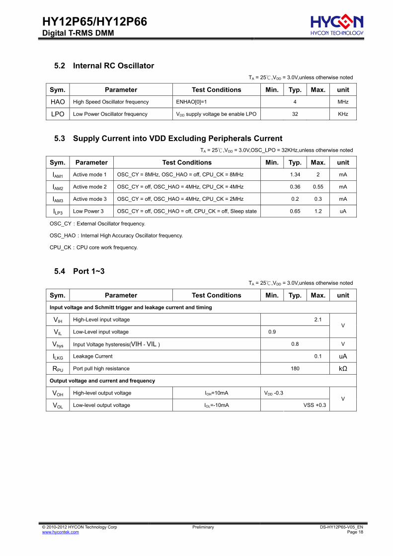
5.2 Internal RC Oscillator TA = 25 ,V DD = 3.0V,unless otherwise noted
Sym. Parameter Test Conditions Min. Typ. Max. unit
HAO High Speed Oscillator frequency ENHAO[0]=1 4 MHz
LPO Low Power Oscillator frequency VDD supply voltage be enable LPO 32 KHz
5.3 Supply Current into VDD Excluding Peripherals Current TA = 25 ,V DD = 3.0V,OSC_LPO = 32KHz,unless otherwise noted
Sym. Parameter Test Conditions Min. Typ. Max. unit
IAM1 Active mode 1 OSC_CY = 8MHz, OSC_HAO = off, CPU_CK = 8MHz 1.34 2 mA
IAM2 Active mode 2 OSC_CY = off, OSC_HAO = 4MHz, CPU_CK = 4MHz 0.36 0.55 mA
IAM3 Active mode 3 OSC_CY = off, OSC_HAO = 4MHz, CPU_CK = 2MHz 0.2 0.3 mA
ILP3 Low Power 3 OSC_CY = off, OSC_HAO = off, CPU_CK = off, Sleep state 0.65 1.2 uA
OSC_CY:External Oscillator frequency.
OSC_HAO:Internal High Accuracy Oscillator frequency.
CPU_CK:CPU core work frequency.
5.4 Port 1~3 TA = 25 ,V DD = 3.0V,unless otherwise noted
Sym. Parameter Test Conditions Min. Typ. Max. unit
Input voltage and Schmitt trigger and leakage current and timing
VIH High-Level input voltage 2.1
VIL Low-Level input voltage 0.9 V
Vhys Input Voltage hysteresis(VIH - VIL ) 0.8 V
ILKG Leakage Current 0.1 uA
RPU Port pull high resistance 180 kΩ
Output voltage and current and frequency
VOH High-level output voltage IOH=10mA VDD -0.3
VOL Low-level output voltage IOL=-10mA VSS +0.3V
.

HY12P65/HY12P66 Digital T-RMS DMM
© 2010-2012 HYCON Technology Corp www.hycontek.com
Preliminary DS-HY12P65-V05_ENPage 19
5.5 Reset(Brownout, External RST pin, Low Voltage Detect) TA = 25 ,V DD = 3.0V,unless otherwise noted
Sym. Parameter Test Conditions Min. Typ. Max. unit
Pulse length needed to accepted reset internally, td-LVR 2 us
VDD Start Voltage to accepted reset internally (LH),VLVR 1.6 1.85 2.1 V BOR
Hysteresis, VHYS-LVR 70 mV
Pulse length needed as RST/VPP pin to accepted reset internally,
td-RST 2 us
Input Voltage to accepted reset internally 0.9 V RST
Hysteresis, VHYS-RST 0.8 V
Operation current, ILVD 10 15 uA
External input voltage to compare reference voltage 1.2 V
Compare reference voltage temperature drift TA = -40 ~ 85 100 ppm/
Detect VDD voltage rang by user option, VSVS VLDx[3:0]=1110b 3.3
Detect VDD voltage rang by user option, VSVS VLDx[3:0]=1101b 3.2
Detect VDD voltage rang by user option, VSVS VLDx[3:0]=1100b 3.1
Detect VDD voltage rang by user option, VSVS VLDx[3:0]=1011b 3.0
Detect VDD voltage rang by user option, VSVS VLDx[3:0]=1010b 2.9
Detect VDD voltage rang by user option, VSVS VLDx[3:0]=1001b 2.8
Detect VDD voltage rang by user option, VSVS VLDx[3:0]=1000b 2.7
Detect VDD voltage rang by user option, VSVS VLDx[3:0]=0111b 2.6
Detect VDD voltage rang by user option, VSVS VLDx[3:0]=0110b 2.5
Detect VDD voltage rang by user option, VSVS VLDx[3:0]=0101b 2.4
Detect VDD voltage rang by user option, VSVS VLDx[3:0]=0100b 2.3
Detect VDD voltage rang by user option, VSVS VLDx[3:0]=0011b 2.2
Detect VDD voltage rang by user option, VSVS VLDx[3:0]=0010b 2.1
LVD
Compare
Mode
Detect VDD voltage rang by user option, VSVS VLDx[3:0]=0001b 2.0
V
Comparator Offset Error -150 150 mV VDD Ratio
Compare Mode VDD Ratio Error -5 5 %
BOR:Brownout Reset
LVR:Low Voltage Reset of BOR
LVD:Low Voltage Detect
RST:External Reset pin
.

HY12P65/HY12P66 Digital T-RMS DMM
© 2010-2012 HYCON Technology Corp www.hycontek.com
Preliminary DS-HY12P65-V05_ENPage 20
Figure6.5-1 BOR reset diagram
.
Figure6.5-2 RST reset diagram
*1 rRST:Please see BOR Introduce of HY12Pxx series User’s Guide (UG-HY12S65-Vxx).
VLVR and VHYS vs. TA
1.700
1.740
1.780
1.820
1.860
1.900
-40 -20 0 20 40 60 80 100
TA
VL
VR
an
d V
HY
S (
V)
VLVR
VHYS
Figure6.5-3 VLVR and VHYS vs. Temperature
.

HY12P65/HY12P66 Digital T-RMS DMM
© 2010-2012 HYCON Technology Corp www.hycontek.com
Preliminary DS-HY12P65-V05_ENPage 21
5.6 Power System TA = 25 ,V DD = 3.0V,unless otherwise noted
Sym. Parameter Test Conditions Min. Typ. Max. unit
VDDA operation current, IVDDA IL = 0mA LDOC[1:0]=00b 22 uA
Select VDDA output voltage IL = 0.1mA,
VDD=3V LDOC[1:0]=00b 3.6 V
Load Regulaion VDD=2.4V
IL = 1~5mA LDOC[1:0]=00b 10 mV
Line Regulation VDD=2.4V~3.6V
IL = 1mA LDOC[1:0]=00b 40 mV
Temperature drift TA=-40 ~85 100 ppm/
VDDA
VDD Voltage drift
LDOC[1:0]=11b
IL = 0.1mA VDD=2.5V~3.6V ±0.2 %/V
AGND operation current, IAgnd IL = 0mA 20 uA
Output voltage ,VAgnd IL = 0uA 1.0 V AGND
Output voltage with Load
SAGND≠00b
IL = ±200uA 0.98 1.02 VAGND
V(REFO,AGND) IL = 0uA 1,2 V
Temperature drift TA=-40 ~85 100 ppm/REFO
RMS Noise
ENLDO=1b,
SAGND≠00b
60 uVrms
5.7 LCD TA = 25 ,V DD = 3.0V, CVLCD =4.7uF,unless otherwise noted.
Sym. Parameter Test Conditions Min. Typ. Max. unit
VDD = 2.2V ILCD
Operation supply current without
output buffer.(all segment turn on)
LCDPR[0]=1
VDD = 3.0V 20 uA
Supply Voltage at VLCD pin LCDPR[0]=0 2.2 3.6 V
VLCDX[1:0]=11b 2.295 2.55 2.805
VLCDX[1:0]=10b 2.52 2.8 3.08
VLCDX[1:0]=01b 2.745 3.05 3.355
VLCD Embedded Charge Pump output
voltage at VLCD pin
VDD = 2.2V,
LCDPR[0]=1,
CVLCD =4.7uF
VLCDX[1:0]=00b 2.97 3.3 3.63
V
ZLCD Output impedance with LCD buffer fLCD =128Hz,VLCD=3.05V 10 kΩ
.

HY12P65/HY12P66 Digital T-RMS DMM
© 2010-2012 HYCON Technology Corp www.hycontek.com
Preliminary DS-HY12P65-V05_ENPage 22
5.8 Σ∆ADC, Power Supply and Recommended Operating Conditions TA = 25 ,V DD = 3.0V, VDDA=3.6V,VR=1.2V, AGND=0.5VDD, ADC Clock=400kHz Input buffer on unless otherwise noted
Sym. Parameter Test Conditions Min. Typ. Max. unit
fΣ∆ADC Modulator sample frequency, ADC_CK 400 KHz
I Σ∆ADC Operation supply current Input gain =0.9, input buffer on
ADC_CK=400KHz 550 uA
OSR=2500~20000 17D79
OSR=64~256 3FFFF DΣ∆ADC Maximum ADC Output
Code (ADC Gain Factor) OSR=32 3FD7C
d
Input gain=0.9,
reference gain=1 20 100
Eos Input offset voltage Chopper on
OSR=20000 Input gain=3.6,
reference gain=0.33 5 10
uV
Input gain=0.9,
reference gain=1 200 600
Rev Roll-over error voltage Chopper on
OSR=20000 Input gain=3.6,
reference gain=0.33 10 30
uV
Chopper on, OSR=20000, input gain=0.9
reference gain=1 10
Chopper on, OSR=20000, input gain=3.6
reference gain=0.33 2
Chopper off, OSR=32, input gain=0.9 reference
gain=1 400
Vrms Input RMS Noise
Chopper off, OSR=32, input gain=3.6 reference
gain=0.33 80
uV
Input gain=0.9,
reference gain=1.
Vin=200mVrms
50/60Hz NM Normal Rejection ratio
Chopper On
OSR=20000
ADCLK=1 Input gain=3.6,
reference gain=0.33.
Vin=20mVrms
50/60Hz
60 dB
0.5% error 20 1.5 ACbw
AC Measurement
Bandwidth
OSR=32,
LPFBW=1024 3dB 6 kHz
.
HY12P65/HY12P66 Digital T-RMS DMM
© 2010-2012 HYCON Technology Corp www.hycontek.com
Preliminary DS-HY12P65-V05_ENPage 23
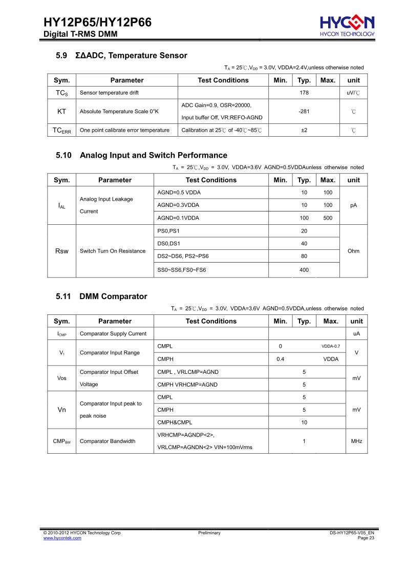
5.9 Σ∆ADC, Temperature Sensor TA = 25 ,V DD = 3.0V, VDDA=2.4V,unless otherwise noted
Sym. Parameter Test Conditions Min. Typ. Max. unit
TCS Sensor temperature drift 178 uV/
KT Absolute Temperature Scale 0°K ADC Gain=0.9, OSR=20000,
Input buffer Off, VR:REFO-AGND-281
TCERR One point calibrate error temperature Calibration at 25 of -40 ~85 ±2
5.10 Analog Input and Switch Performance
TA = 25 ,V DD = 3.0V, VDDA=3.6V AGND=0.5VDDAunless otherwise noted
Sym. Parameter Test Conditions Min. Typ. Max. unit
AGND=0.5 VDDA 10 100
AGND=0.3VDDA 10 100 IAL Analog Input Leakage
Current AGND=0.1VDDA 100 500
pA
PS0,PS1 20
DS0,DS1 40
DS2~DS6, PS2~PS6 80 Rsw Switch Turn On Resistance
SS0~SS6,FS0~FS6 400
Ohm
5.11 DMM Comparator
TA = 25 ,V DD = 3.0V, VDDA=3.6V AGND=0.5VDDA,unless otherwise noted
Sym. Parameter Test Conditions Min. Typ. Max. unit
ICMP Comparator Supply Current uA
CMPL 0 VDDA-0.7
VI Comparator Input Range CMPH 0.4 VDDA
V
CMPL , VRLCMP=AGND 5 Vos
Comparator Input Offset
Voltage CMPH VRHCMP=AGND 5 mV
CMPL 5
CMPH 5 Vn Comparator Input peak to
peak noise CMPH&CMPL 10
mV
CMPBW Comparator Bandwidth VRHCMP=AGNDP<2>,
VRLCMP=AGNDN<2> VIN=100mVrms 1 MHz
.

HY12P65/HY12P66 Digital T-RMS DMM
© 2010-2012 HYCON Technology Corp www.hycontek.com
Preliminary DS-HY12P65-V05_ENPage 24
6. Ordering Information
Device No.1 Package
Type Pins
Package
Drawing Code2
Shipment
Packing
Type
Unit
Q’ty
Material
CompositionMSL3
HY12P65-D000 Die - D 000 000 - 100 Green4 -
HY12P65-L064 LQFP 64 L 064 000 Tray 250 Green4 MSL-3
1 Device No.: Model No. – Package Type Description – Code (Blank Code/ Standard/
Customized Programming Code)
Ex: Your customized programming code is 008 and you require die shipment.
The device No. will be HY12P65-D000-008.
Ex: You request blank code in die package.
The device No. will be HY12P65-D000.
Ex: You request blank code in LQFP 64 package.
The device No. will be HY12P65-L064.
And please clearly indicate the shipment packing type when placing orders.
Ex: Your customized programming code is 008 and you require products in LQFP 64
package.
The device No. will be HY12P65-L064-008.
And please clearly indicate the shipment packing type when placing orders. 2 Code :
“001”~ “999” is standard or customized programming code.
Blank code does not have these numbers. 3 MSL:
The Moisture Sensitivity Level ranking conforms to IPC/JEDEC J-STD-020 industry
standard categorization.
The products are processed, packed, transported and used with reference to
IPC/JEDEC J-STD-033. 4 Green (RoHS & no Cl/Br):
HYCON products are Green products that compliant with RoHS directive and are
Halogen free (Br/Cl<0.1%)
.

HY12P65/HY12P66 Digital T-RMS DMM
© 2010-2012 HYCON Technology Corp www.hycontek.com
Preliminary DS-HY12P65-V05_ENPage 25
7. Packaging Information
JEDEC MS-026 Compliant
.
HY12P65/HY12P66 Digital T-RMS DMM
© 2010-2012 HYCON Technology Corp www.hycontek.com
Preliminary DS-HY12P65-V05_ENPage 26
8. Revision Record Major differences are stated thereinafter:
Version Page Revision Summary
V02 All First edition
V03 6~16
18
22
Updated the figures (removed SPI function)
Revised chapter 5.3 Supply Current into VDD excluding Peripherals Current
information.
ADC max. Output code revision
5 Add HY12P66 Difference V04
11~12 Reviser Pin Description (Pin12~Pin34)
8 Revise ADC diagram V05
16 Revise register error
.


![Presentación de PowerPoint - Vanities International · 1/8" [3.2] 1/8" [3.2] FT-4x15-GT-Chevrons 1 1 Vanities International 400 Johnson Road Mooresville, IN 46158 317-831-2717 .](https://static.documents.pub/doc/80x56/5f3af2629a63780da87f5b02/presentacin-de-powerpoint-vanities-international-18-32-18-32.jpg)


![4x17 8 4x19 8,dowels%20pins4x6 4 5x4 5 bearing rollers 4x15 8 4x17 8 4x19 8 4x21 8[1]](https://static.documents.pub/doc/80x56/5790744d1a28ab6874af45b9/4x17-8-4x19-8dowels20pins4x6-4-5x4-5-bearing-rollers-4x15-8-4x17-8-4x19-8.jpg)

