Guoqing Deng∗ and Chunhong ChenDepartment of Electrical and Computer Engineering, University of Windsor, Windsor, Ontario, Canada
Hybrid CMOS-SET architectures, which combine the merits of CMOS and single electron transistor(SET) devices, promise to be a practical implementation for nanometer scale circuit design. In thiswork, we propose the design of two typical arithmetic circuits, namely adder and multiplier, usinghybrid CMOS-SET architectures. For full adders (FAs) design, we present three different implemen-tations based on multiple-valued logic (MVL), phase modulation and frequency modulation. TheseFAs fully utilize SET’s unique characteristic of Coulomb blockade oscillation and exhibit improvedperformance in terms of circuit area/complexity, power dissipation and temperature effect. The struc-ture based on frequency modulation also possesses high immunity against background charges,and is extended to design of multiple-bit adder and multiplier.
Keywords: Hybrid, Single Electron Transistor (SET), Multiple-Valued Logic (MVL), Modulation,Coulomb Blockade Oscillation, Power Dissipation, Background Charges.
1. INTRODUCTION
The scale-down of CMOS technology will inevitably hitthe point where the quantum mechanical effect becomespredominant and hence makes it impossible to furthershrink MOSFET dimensions.1 One possible candidatefor next generation electronics is single-electron-tunnelingtechnology.2 As one of the most sophisticated single elec-tron devices (SED), single electron transistor (SET) isexpected to be quite promising for future VLSI designdue to its nanoscale feature-size, ultra low power dis-sipation and unique characteristic of Coulomb blockadeoscillation.3 Circuits with SETs are also able to achievea lot of new functionalities with less number of devicesthrough novel design methodologies. However, pure SET-based circuits have very limited applications due to SET’slow current drivability, small voltage gain and extremelylow-temperature operation.4 Since CMOS devices haveadvantages that can compensate for the intrinsic drawbacksof SET, hybrid CMOS-SET architecture which combinesthe merits of both CMOS and SET devices promises tobe a much practical implementation for nanometer-scalecircuit design.5
Full adder (FA) and multiplier are key elements forarithmetic operation. It is therefore of special interestto design these arithmetic circuits with extremely smallsize and ultra-low power dissipation. Extensive researchwork has been done on full adder design with SET
∗Author to whom correspondence should be addressed.
technology, utilizing a variety of logic such as majoritygate (MAJ),6�7 threshold logic gate (TLG),8 pass-transistorlogic (PTL),9 binary decision diagram (BDD),10 and manyothers.11–14 While these pure SED-based adders dramat-ically reduce circuit area and power dissipation, theycan only work at extremely low temperature (less than10 K) due to the crucial limitation of thermal effect,making them impractical for real applications. SeveralFAs using hybrid CMOS-SET architecture have also beenreported recently with increased temperature operation (upto room temperature).15–19 However, many of them15–17
simply adopted conventional CMOS structures which didnot adequately take advantage of new characteristics ofSETs. Some hybrid FAs18�19 did utilize Coulomb blockadeoscillation characteristic that further reduces the numberof devices, the less regularity of these circuits made themnot suitable for VLSI design. Also, the background chargeeffect is a critical issue on circuit reliability, which hasnot been taken into account in the above FAs. Since mul-tiplication can generally be viewed as repeated shifts andadds, multipliers can, in principle, be implemented easilyin CMOS technology using only adders, shift registers anda certain amount of control logic. However, to the best ofour knowledge, there is little research on multiplier designbased on SET devices for significant improvement in bothcircuit area and power dissipation.In this work, we propose three different implementa-
tions for hybrid CMOS-SET FAs by using multiple-valuedlogic (MVL), phase modulation and frequency modulation,with the goal of improving circuit area and complexity,
Hybrid CMOS-SET Arithmetic Circuit Design Using Coulomb Blockade Oscillation Characteristic Deng and Chen
power dissipation and temperature effects. In particular, itis found that the structure based on frequency modulationshows high immunity against background charges, and ishence utilized to implement multiple-bit adders and mul-tipliers as well. Throughout the work, MIB (named afterauthors in)20 analytical model is used for SETs and allsimulations are conducted using conventional SPICE sim-ulator in Cadence at room temperature.21
2. BACKGROUND
SET is made of two tunnel junctions that share a commonelectrode, known as the island, with capacitively coupledgate terminals. A tunnel junction consists of two pieces ofmetal separated by a very thin (∼1 nm) insulator.3 Accord-ing to the laws of classical electromagnetism, no currentcan flow through an insulating barrier. From the viewpointof quantum mechanics, however, there is a non-vanishingprobability for electrons to pass through the tunnel junc-tion. Based on the orthodox theory which provides theunique guiding rules in single electronics,2 the tunneling ofsingle electron through a tunnel junction is always a ran-dom event with a certain rate (also known as the tunnelingrate) that depends solely on the reduction of free energy ofthe system as a result of this tunneling event.3 Therefore,from the microscopic point of view, the electron tunnelingevent is a stochastic process. From the macroscopic per-spective, the current flowing through a tunnel junction is adeterministic behavior which depends on different externalvoltage or current biasing conditions.For voltage/current biased SETs, the output drain cur-
rent/voltage of SET exhibits an oscillating characteristicwith respect to SET’s input gate voltage. This phenomenonis known as Coulomb blockade oscillation. It is well under-stood that the amplitude and period of the oscillation curveare inversely proportional to C∑ (i.e., the total capacitanceon the island of SET with respect to the ground) and CG
(i.e., the input gate capacitance), respectively. The phaseof oscillation curve can be adjusted by the voltage appliedon SET’s second gate with no effects on its amplitude andperiod. For the Coulomb blockade oscillation to occur, twocriteria must be satisfied:(1) SET’s drain-to-source voltage (i.e., VDS-SET) should beless than 3e/2C∑. It has been observed that if e/2C∑ <VDS-SET < 3e/2C∑, the Coulomb blockade region will dis-appear but the Coulomb oscillation remains. If VDS-SET >3e/2C∑, the Coulomb oscillation phenomenon vanishesout and SET functions as a regular resistor;(2) the operating temperature should be very low (typi-cally no more than 10 K). At a higher temperature, thethermal energy will significantly affect the electron tun-neling rate with the likelihood of making tunneling eventsout of control.
With hybrid CMOS-SET architecture, the sub-ambienttemperature operation (i.e., −150 �C∼−50 �C) can be
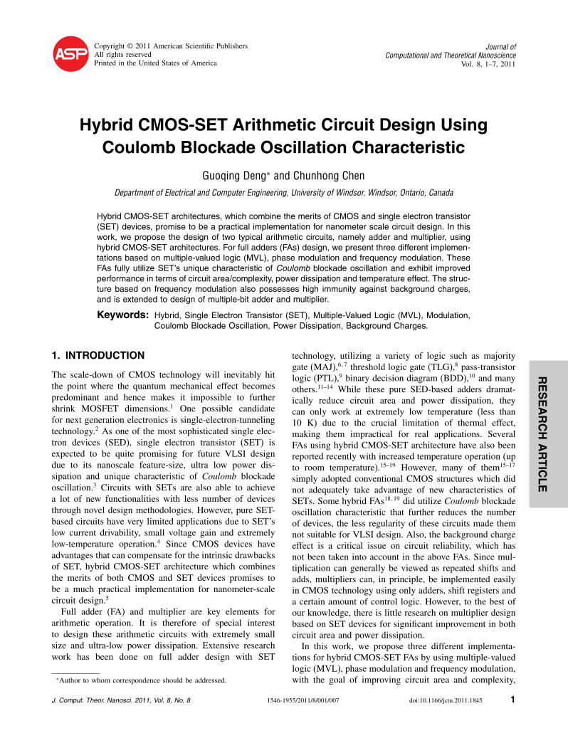
(a) (b)
Fig. 1. (a) Serial SETMOS and (b) parallel SETMOS.
realized, thanks to the large voltage gain of MOSFETs.4
If SET’s device dimensions are further reduced so that C∑
is at the range of several aF, hybrid CMOS-SET circuitswill be able to work at room temperature. There are twowidely used hybrid CMOS-SET architectures,5 as shownin Figures 1(a) and (b) (in the remainder of the paper,they are called serial SETMOS and parallel SETMOS,respectively), where VGG and VSS are used to bias NMOStransistors to work at sub-threshold region and VPC (‘PC’stands for phase control) is used to adjust the phase ofvoltage oscillation at VDS-SET. Due to the constant currentbiasing for NMOS transistor, VDS-SET oscillation can betransferred and amplified to the output node (i.e., VOUT). Inorder to keep VDS-SET less than 3e/2C∑, the biasing cur-rent through SET should be at the range of several tens ofnA, which makes the current drivability of serial SETMOSvery small. However, with separate biasing currents in par-allel SETMOS (the one used to bias NMOS transistor isat the range of several �A), a higher current drivability atthe output can be achieved.
3. THREE IMPLEMENTATIONS OF 1-BITHYBRID CMOS-SET FAs
3.1. Multiple-Valued Logic (MVL) Scheme
For a current biased SET, due to holes accumulation atSET’s drain terminal, electrons induced from the groundwill tunnel through both source and drain junctions of SETvia the island, leading to a tunneling current. At steadystate, the tunneling current equals to SET’s biasing current,which means that the number of electrons which success-fully pass through SET’s junctions equals to the number ofholes accumulated at SET’s drain terminal per unit time.The excess number of accumulated holes during the tran-sient response contributes to SET’s drain voltage. SinceSET’s input gate voltage has the impact on electron tun-nelling rate, it also affects the net amount of holes at SET’sdrain terminal (i.e., VDS-SET) at the steady state. In otherwords, the SET can be considered as a tunable resistorwhose resistance is controlled by the voltage applied onSET’s gate terminal.
2 J. Comput. Theor. Nanosci. 8, 1–7, 2011
RESEARCH
ARTIC
LE
Deng and Chen Hybrid CMOS-SET Arithmetic Circuit Design Using Coulomb Blockade Oscillation Characteristic
Let us consider three SETs connected in parallel, asshown in Figure 2(a) where all three SETs are identi-cal with the same second gate biasing voltage VPC. Thisstructure is analogous to three parallel resistors. Throughappropriate configuration, each SET reaches its minimum(or maximum) resistivity with its input gate voltage (i.e.,VIN) being logic ‘0’ (or ‘1’). As a result, if all three inputsare logic ‘0’, the total equivalent resistance (i.e., Req� ofthree SETs is minimal, and thus VDS-SET reaches its min-imum value. As the number of 1’s in the input increases,so do the values of Req and VDS-SET. With all three inputsbeing logic ‘1’, Req and VDS-SET will reach their maximumvalues. More specifically, as shown in Figure 2(b), if oneinput voltage (say VIN-A) increases from zero to a consid-erable value with two other inputs being:(1) both logic ‘0’,(2) logic ‘0’ for one and logic ‘1’ for the other, or(3) both logic ‘1’, one can observe three voltage oscil-lation curves at VDS-SET which have the same period andphase but different voltage levels.
In terms of digital applications, six points (i.e., P0∼P5 inthe figure) can be obtained from the three curves located atfour different voltage levels (i.e., V 0∼V 3) which representeight input patterns (i.e., 000, 001, � � � � 111).
In order to realize Carry and Sum functions for theadder design, the four intermediate voltage values need tobe properly re-allocated into two voltage levels. A parallelSETMOS can be used to realize such a voltage conversion.By adjusting the period and phase of VDS-SET oscillation,the output voltage oscillation of parallel SETMOS can beconfigured to the pattern as shown in Figure 2(c), in orderto generate Carry and Sum outputs. The overall schematicof 1-bit FA using the above MVL scheme is shown inFigure 2(d).Parallel connected multiple-SET architecture can also
be used to implement D/A converters. Since SET can beregarded as a voltage controlled tunable resistor, the equiv-alent resistance of all SETs and hence the correspondingvoltage at VDS-SET can be modulated to represent the valueof digital inputs rather than the number of 1’s in the inputsas long as each individual SET is properly weighted.
3.2. Phase Modulation Scheme
Instead of applying the inputs on three SETs, one canuse only one SET with multiple input gates to accommo-date three input digits, as shown in Figure 3(a) where thethree left-hand-side gates of SET are identical and usedto accept three input digits, and the fourth right-hand-side gate of SET is used to adjust the phase of voltageoscillation at VDS-SET. This is known as phase modulationscheme. Unlike the MVL scheme which moves VDS-SEToscillation vertically, the phase modulation scheme movesVDS-SET oscillation horizontally based on different inputpatterns.
(a)
(b)
(c)
(d)
Fig. 2. (a) Parallel SETMOS with three SETs connected in parallel.(b) Voltage oscillations at VDS-SET and voltage conversion through NMOStransistor. (c) Voltag oscillations at output used to realize Carry and Sumfunctions. (d) Overall schematic of 1-bit FA based on MVL scheme.
By adjusting the device capacitance of SET and biasingvoltage VPC, the VDS-SET oscillation (as a result of increas-ing one input) can be configured to the pattern as shownin Figure 3(b) where the axes Y0, Y1 and Y2 correspondto the condition of two other inputs being:(1) both logic ‘0’,(2) logic ‘0’ for one and logic ‘1’ for the other, or(3) both logic ‘1’, respectively.
It is observed that eight input patterns (i.e., 000, 001, � � � �111) are well distributed at four points (i.e., P0∼P3) onthe oscillation curve. For the Sum function, a half-periodphase shift occurs each time one input digit alters its logicvalue. For the Carry function, since the period is doubled,only one-fourth period phase shift is obtained under the
J. Comput. Theor. Nanosci. 8, 1–7, 2011 3
RESEARCH
ARTIC
LE
Hybrid CMOS-SET Arithmetic Circuit Design Using Coulomb Blockade Oscillation Characteristic Deng and Chen
(a) (b)
Fig. 3. (a) Overall schematic of 1-bit FA using phase modulation scheme. (b) Voltage oscillations at VDS-SET used to realize Sum and Carry functions.
same operation. Both Carry and Sum outputs can be imple-mented using the same circuit architecture with differentparameters.
3.3. Frequency Modulation Scheme
It should be noticed that the previous two schemes forFAs strongly depend on particular voltages at the operat-ing point. They work properly with no background chargeson SETs. However, with background charges which arerandom in nature and cannot be entirely removed bytoday’s technology,22 the above circuits may fail to func-tion correctly, depending on the amount of charges. Inorder to construct a robust hybrid CMOS-SET FA againstbackground charge fluctuation, we propose yet anotherscheme—frequency modulation scheme—as follows.The circuit structure based on frequency modulation
scheme is shown in Figure 4(a), where three left-hand-sidegates of SET are identical and directly connected to threeNMOS transistors that function as switches. The digitalinputs are used to control NMOS switches (on or off).Vs is a monotonically increase voltage applied via NMOSswitches on SET’s input gate terminals. Due to the fact thatthe node capacitance between NMOS and SET devices isrelatively large (at the range of several fF), SET’s inputgate capacitance (at the range of several aF) in such astructure would not be affected by the NMOS devices.With Vs applied on any of SET’s input gate terminals,the period of voltage oscillation at VDS-SET is inverselyproportional to SET’s input gate capacitance. If the Vs
is applied on multiple input gates of SET, the period ofVDS-SET oscillation is determined by the total capacitanceof those gates connected with Vs. Since three input digitsapplied on NMOS switches are able to control the connec-tion between Vs and input gates of SET, the total input gate
capacitance and hence the period of VDS-SET oscillationis defined by different input patterns. When Vs increasesfrom zero to VTOP, as shown in Figure 4(b), the number of1’s in the inputs is modulated into the number of voltageoscillation cycles at VDS-SET.
Due to the high operating speed of SET, the oscil-lation at VDS-SET is reflected into the time domain. Byusing a 2-bit ripple counter, the number of voltage oscil-lation cycles at the output with respect to time is recordedin the binary system, and the counter’s outputs representthe Carry and Sum bits. As long as background chargeson the island of SET keep constant during the periodof varying Vs, the same number of voltage oscillationcycles will appear at the output. Since the amount of back-ground charges on SET’s island varies at a relatively lowfrequency,22 the circuit will exhibit much higher immunityagainst background effect.
4. APPLICATIONS USING FREQUENCYMODULATION SCHEME
4.1. Multiple-Bit Full Adders
The frequency modulation scheme can also be used toimplement multiple-bit FAs and multipliers. For the caseof FAs, to accept higher-order input bits, one simply needsto add more input gates for the SET, which are connectedvia NMOS switches with Vs, and the higher-order outputbits can be obtained by adding more cells for the ripplecounter.As an example, Figure 5(a) shows the overall schematic
of 2-bit FA, where the input gate capacitances for x1 andy1 are twice as much as those for x0 and y0, and threeD flip-flops are used to generate the three output bits. Forn-bit FA in general, the SET will have (2n+1) input gates
4 J. Comput. Theor. Nanosci. 8, 1–7, 2011
RESEARCH
ARTIC
LE
Deng and Chen Hybrid CMOS-SET Arithmetic Circuit Design Using Coulomb Blockade Oscillation Characteristic
(a)
(b)
Fig. 4. (a) Overall schematic of 1-bit FA using frequency modulation scheme. (b) Voltage oscillations at VDS-SET.
whose capacitance corresponding to the ith (with i start-ing from 1) input bit is i times as much as that for theleast significant input bit, and the number of D flip-flopsfor the ripple counter is n+1. Since each D flip-flop canbe implemented with minimum of 8 MOS transistors, thetotal number of MOS transistors needed is �2n+1�+1+8n = 10n+ 2. With CMOS technology, n-bit ripple carryadder requires 24nMOS transistors, which is the minimumhardware required for n-bit FA. The n-bit hybrid CMOS-SET FA using frequency modulation scheme dramaticallyreduces the circuit area and power dissipation, especiallyfor a large value of n (the area and power consumed bySET device are negligible compared to CMOS devices).
4.2. Multiple-Bit Multipliers
In the structure based on frequency modulation scheme,the number of voltage oscillation cycles at the output isnot only determined by the total input gate capacitanceof SET, but also affected by the varying range of Vs. Forinstance, if the range of Vs is two times greater, the num-ber of voltage oscillation cycles will double. Therefore,by setting a maximum value of Vs based on multiplicand(using a D/A converter) and the total input gate capaci-tance based on multiplier, the number of voltage oscillationcycles at the output will represent the multiplication of thetwo operands.Another method to realize multiplication is through a
cascaded structure of parallel SETMOSs. It is understood
that parallel SETMOS is able to generate voltage oscil-lation at the output by monotonically changing (eitherincreasing or decreasing) Vs. If the Vs is chosen to be acycle (say, increasing from zero to a certain value thenreturning back to zero), as long as the dynamic ranges ofinput and output voltage are the same, each output voltageoscillation cycle can serve as the voltage Vs for the nextparallel SETMOS. Therefore, with two parallel SETMOSsconnected in serial, where each of them is configured byan operand (whose value is assumed to be N) in such away that one cycle of Vs will generate N cycles of out-put voltage, the number of voltage oscillation cycles at theoutput of the second parallel SETMOS will represent themultiplication of the two operands.Figure 5(b) shows the overall schematic of 3-bit mul-
tiplier using the cascaded structure of two parallel SET-MOSs, where the input gate capacitances of SET shouldbe weighed properly for each operand. The circuit canalso perform multiplication with multiple operands usingmultiple stages, and each stage can be designed to acceptmore than one operand (using the structure in Fig. 5(a))so that the addition and multiplication operations can beperformed simultaneously.
5. PARAMETER SELECTION OF THEPROPOSED CIRCUITRS
All proposed hybrid CMOS-SET circuits share the sameparameters of RTD =RTS = 1 M� and CTD = CTS = 0�1 aF
J. Comput. Theor. Nanosci. 8, 1–7, 2011 5
RESEARCH
ARTIC
LE
Hybrid CMOS-SET Arithmetic Circuit Design Using Coulomb Blockade Oscillation Characteristic Deng and Chen
(a)
(b)
Fig. 5. (a) Overall schematic of 2-bit FA using frequency modulation scheme. (b) Overall schematic of 3-bit multiplier using cascaded structure oftwo parallel SETMOSs.
(SET’s source and drain junction resistance and capac-itance), ID1 = 40 nA (SET’s biasing current), ID2 =1 uA (biasing current for NMOS transistor), VTH-NMOS =150∼200 mV (threshold voltage of NMOS transistor), andT = 300 K (operating temperature). Other parameters usedin the structures of three FAs (i.e., in Figs. 2(d), 3(a) and4(a)) are listed in Table I. Figure 6 shows the simulationresult of MVL based FA using the provided parameters.To simulate the circuit based on frequency modulation,
extra control units are needed so that the ripple counter isinitialized to zero each time before the evaluating opera-tion (i.e., get the output by changing Vs). For multiple-bitadders and multipliers, as shown in Figures 5(a) and (b),
Table I. SET’s gate capacitance and biasing voltage used in three FAs.
Sum circuit CG1 = 0�2 aF, CG2 = 0�1 aFVPC−S = 600 mV
Based on frequency modulation CG1 = CG2 = 0�1 aFVPC =−450 mV
Fig. 6. Simulation result of FA based on MVL scheme using parametersin Table I.
CG1 and CG2 are the same as those used in FA based onfrequency modulation but the values of VPC are different.
6. CONCLUSIONS
We have proposed three hybrid CMOS-SET full addersbased on multiple-valued logic (MVL), phase modulationand frequency modulation. For the MVL scheme, SET isconsidered as a voltage controlled tunable resistor. Thismethod can also be used to implement D/A converters. For
6 J. Comput. Theor. Nanosci. 8, 1–7, 2011
RESEARCH
ARTIC
LE
Deng and Chen Hybrid CMOS-SET Arithmetic Circuit Design Using Coulomb Blockade Oscillation Characteristic
the phase modulation scheme, the Carry and Sum func-tions are realized by changing the phase of voltage oscil-lation. In the frequency modulation scheme, the voltageoscillation is reflected in the time domain, and the outputis generated by counting the number of oscillation cycles.With this method, a higher immunity against backgroundcharges is achieved when the circuit works at a relativelyhigh frequency. The frequency modulation scheme has alsobeen utilized easily to implement multiple-bit adders andmultipliers.
Acknowledgments: This work was supported in partby the Natural Sciences and Engineering Research Councilof Canada (NSERC).
References
1. Y. Taur, D. A. Wei Chen Frank, D. J. Ismail, K. E. Shih-Hsien LoSai-Halasz, G. A. Viswanathan, R. G. Wann, H.-J. C. Wind, and S. J.Hon-Sum Wong, Proc. IEEE 85, 486 (1997).
2. C. Wasshuber, Computational Single-Electronics, Springer-Verlag(2001).
3. K. K. Likharev, Proc. IEEE 87, 606 (1999).4. K. Uchida, J. Koga, R. Ohba, and A. Toriumi, Room-temperature
operation of multifunctional single-electron transistor logic, Techni-cal Digest of 2000 IEEE International Electron Devices Meeting(IEDM), pp. 863–865.
5. S. Mahapatra and A. M. Ionescu, Hybrid CMOS Single-Electron-Transistor Device and Circuit Design, Artech House, Inc. (2006).
6. H. Iwamura, M. Akazawa, and Y. Amemiya, IEICE Trans. Electron.E81, 42 (1998).
7. T. Oya, T. Asai, T. Fukui, and Y. Amemiya, IEEE Trans. Nanotech.2, 15 (2003).
8. C. Lageweg, S. D. Colofan, and A. S. Vassiliadis, A full adder imple-mentation using SET based linear threshold gates, Proc. Intl. Conf.
Electr. Circ. Sys. ICECS ’02, September (2002), pp. 665–668.9. Y. Ono, H. Inokawa, and Y. Takahashi, IEEE Trans. Nanotech. 1, 93
(2002).10. N. Asahi, M. Akazawa, and Y. Amemiya, IEEE. Trans. Electron
Devices 44, 1109 (1997).11. M. Sulieman and V. Beiu, On single electron technology full adders,
Proc. IEEE Conf. Nanotech. IEEE NANO’04, August (2004).12. C. Lageweg, Binary Addition Based on Single Electron Tunneling,
IEEE Conf. Nanotech. pp. 327–330.13. S. Cotofana, C. Lageweg, and S. Vassiliadis, IEEE Trans. Computers
54, 243 (2005).14. S. E. Rehan, A novel half-adder using single electron tunneling
technology, IEEE Intl. Conf. Nano/Micro Engineered and MolecularSystems, NEMS ’07, 2nd edn., January (2007), pp. 245–249.
15. H. Inokawa and Y. Takahashi, A Single-Electron-Transistor LogicGate Family and Its Application-Part II: Design and Simulationof a 7–3 Parallel Counter with Linear Summation and Muptiple-Valued Latch Functions, Proc. 34th Intl. Symp. Multiple-ValuedLogic, ISMVL ’04, May (2004), pp. 262–268.
16. A. Venkataratnam and A. K. Goel, Design and simulation of logiccircuits with hybrid architectures of single electron transistors andconventional devices, 1st Intl. Conf. Nano-Networks and Workshops,2006. NanoNet ’06, September (2006), pp. 1–5.
17. H. Inokawa, A. Fujiwara, and Y. Takahashi, A multiple-valued logicwith merged single-electron and MOS transistors, Electron DevicesMeeting, 2001, IEDM Technical Digest, Intl., December (2001),pp. 721–724.
18. L. Qin, C. Li, Z. Youjie, W. Gang, and W. Sen, Design and simu-lation of logic circuits by combined single electron and MOS tran-sistor structures, Proc. IEEE Intl. Conf. Nan/Micro Engineered andMolecular Sys., January (2008).
19. Y. Seop, Yu et al., Semiconductor Science and Technology 647(2007).
20. S. Mahapatra et al., IEEE Trans. Electron Devices 51, 1772 (2004).21. S. Mahapatra et al., A CAD framework for co-design and analysis
of CMOS-SET hybrid integrated circuits, Proc. of 2003 IEEE22. H. Grabert and M. H. Devoret, Single Charge Tunneling: Coulomb
Blockade Phenomena in Nanostructures, Springer-Verlag (1992).
Received: 21 September 2010. Accepted: 23 January 2011.