Abstract: We show, via simulations, that an optical fiber taper waveguidecan be an efficient tool for photoluminescence and resonant, extinctionspectroscopy of single emitters, such as molecules or colloidal quantumdots, deposited on the surface of a thin dielectric membrane. Placed overa high refractive index membrane, a tapered fiber waveguide induces theformation of hybrid mode waves, akin to dielectric slotted waveguidemodes, that provide strong field confinement in the low index gap re-gion. The availability of such gap-confined waves yields potentially highspontaneous emission enhancement factors (≈ 20), fluorescence collectionefficiencies (≈ 23 %), and transmission extinction (≈ 20 %) levels. A factorof two improvement in fluorescence and extinction levels is predicted if themembrane is instead replaced with a suspended channel waveguide. Twoconfigurations, for operation in the visible (≈ 600 nm) and near-infrared(≈ 1300 nm) spectral ranges are evaluated, presenting similar performances.
OCIS codes: (350.4238) Nanophotonics and photonic crystals; (270.0270) Quantum optics.
References and links1. V. R. Almeida, Q. Xu, C. A. Barrios, and M. Lipson, “Guiding and confining light in void nanostructure,” Opt.
Lett. 29, 1209–1211 (2004).2. A. H. J. Yang, S. D. Moore, B. S. Schmidt, M. Klug, M. Lipson, and D. Erickson, “Optical manipulation of
nanoparticles and biomolecules in sub-wavelength slot waveguides,” Nature 457, 71–75 (2009).3. C. Koos, P. Vorreau, T. Vallaitis, P. Dumon, W. Bogaerts, R. Baets, B. Esembeson, I. Biaggio, T. Michinobu,
F. Diederich, W. Freude, and J. Leuthold, “All-optical high-speed signal processing with silicon-organic hybridslot waveguides,” Nat. Photon. 3, 216–219 (2009).
4. Y. C. Jun, R. M. Briggs, H. A. Atwater, and M. L. Brongersma, “Broadband enhancement of light emissioninsilicon slot waveguides,” Opt. Express 17, 7479–7490 (2009),http://www.opticsexpress.org/abstract.cfm?URI=oe-17-9-7479
5. W. Moerner, “Examining nanoenvironments in solids on the scale of a single, isolated inpurity molecule,” Science265, 46–53 (1994).
6. W. E. Moerner, “Single-photon sources based on single molecules in solids,” N. J. Phys. 6, 88 (2004).7. J. Hwang, M. Pototschnig, R. Lettow, G. Zumofen, A. Renn, S. Gotzinger, and V. Sandoghdar, “A single-
molecule optical transistor,” Nature 460, 76–80 (2009).8. K. Srinivasan, O. Painter, A. Stintz, and S. Krishna, “Single quantum dot spectroscopy using a fiber taper waveg-
uide near-field optic,” Appl. Phys. Lett. 91, 091102 (2007).
#124500 - $15.00 USD Received 9 Dec 2009; revised 26 Feb 2010; accepted 10 Mar 2010; published 7 Apr 2010(C) 2010 OSA 24 May 2010 / Vol. 18, No. 11 / OPTICS EXPRESS 10995
9. M. Davanco and K. Srinivasan, “Efficient spectroscopy of single embedded emitters using optical fiber taperwaveguides,” Opt. Express 17, 10542–10563 (2009).
10. M. Davanco and K. Srinivasan, “Fiber-coupled semiconductor waveguides as an efficient optical interface to asingle quantum dipole,” Opt. Lett. 34, 2542–2544 (2009),http://ol.osa.org/abstract.cfm?URI=ol-34-16-2542
11. A. W. Snyder and J. D. Love, Optical Waveguide Theory (Chapman and Hall, New York, NY, 1983).12. I. Gerhardt, G. Wrigge, P. Bushev, G. Zumofen, M. Agio, R. Pfab, and V. Sandoghdar, “Strong Extinction of a
Laser Beam by a Single Molecule,” Phys. Rev. Lett. 98, 033601 (2007).13. J. Lee, V. C. Sundar, J. R. Heine, M. G. Bawendi, and K. F. Jensen, “Full Color Emission from II-VI Semicon-
ductor Quantum Dot-Polymer Composites,” Adv. Mater. 12, 1102–1105 (2000).14. R. D. Schaller, M. A. Petruska, and V. Klimov, “Tunable Near-Infrared Optical Gain and Amplified Spontaneous
Emission Using PbSe Nanocrystals,” J. Phys. Chem. B 107, 13765–13768 (2003).15. A. Zumbusch, L. Fleury, R. Brown, J. Bernard, and M. Orrit, “Probing individual two-level systems in a polymer
by correlation of single molecule fluorescence,” Phys. Rev. Lett. 70, 3584–3587 (1993).16. M. Orrit and J. Bernard, “Single pentacene molecules detected by fluorescence excitation in a p-terphenyl crys-
tal,” Phys. Rev. Lett. 65, 2716–2719 (1990).17. G. S. Harms, T. Irngartinger, D. Reiss, A. Renn, and U. P. Wild, “Fluorescence lifetimes of terrylene in solid
matrices,” Chem. Phys. Lett. 313, 533–538 (1999).18. T. Bottger, C. W. Thiel, Y. Sun, and R. L. Cone, “Optical decoherence and spectral diffusion at 1.5 μ in
Er3+:Y2SiO5 versus magnetic field, temperature, and Er3+ concentration,” Phys. Rev. B: Condens. Matter Mater.Phys. 73, 075101 (2006).
19. W.-P. Huang, “Coupled-mode theory for optical waveguides: and overview,” J. Opt. Soc. Am. A 11, 963–983(1994).
20. Following Ref. [19], the fiber mode fraction, Eq. (2), would be given by the expression fm =〈 f |m〉〈m| f 〉(〈 f | f 〉〈m|m〉)−1, where 〈 f |m〉 =
∫∫ (e f ×h∗
m +h f × e∗m) · z dS/4. Considering no reflections at the
interface between the isolated fiber and the contact region, (i.e., the field just after the interface is identical to theincident, foward propagating, field), Eq. (2) gives the same result.
21. S. J. van Enk, “Atoms, dipole waves, and strongly focused light beams,” Phys. Rev. A 69, 043813 (2004).22. F. Wise, “Lead salt quantum dots: The limit of strong quantum confinement,” Acc. Chem. Res. 33, 773–780
(2000).23. R. J. Pfab, J. Zimmermann, C. Hettich, I. Gerhardt, A. Renn, and V. Sandoghdar, “Aligned terrylene molecules
in a spin-coated ultrathin crystalline film of p-terphenyl,” Chem. Phys. Lett. 387, 490–495 (2004).24. V. S. C. M. Rao and S. Hughes, “Single quantum-dot Purcell factor and beta factor in a photonic crystal waveg-
uide,” Phys. Rev. B 75, 205437 (2007).25. G. Lecamp, P. Lalanne, and J. P. Hugonin, “Very Large Spontaneous-Emission beta Factors in Photonic-Crystal
Waveguides,” Phys. Rev. Lett. 99 (2007).26. G. Wrigge, I. Gerhardt, J. Hwang, G. Zumofen, and V. Sandoghdar, “Efficient coupling of photons to a single
molecule and the observation of its resonance fluorescence,” Nat. Phys. 4, 60–66 (2008).27. M. T. Rakher, R. Bose, C. W. Wong, and K. Srinivasan, “Spectroscopy of 1.55 μm PbS Quantum Dots on Si
Photonic Crystal Cavities with a Fiber Taper Waveguide,” arXiv:0912.1365v1 (2009).28. M. W. McCutcheon and M. Loncar, “Design of a silicon nitride photonic crystal nanocavity with a Quality factor
of one million for coupling to a diamond nanocrystal,” Opt. Express 16, 19136–19145 (2008),http://www.opticsexpress.org/abstract.cfm?URI=oe-16-23-19136
29. R. F. Oulton, V. J. Sorger, T. Zentgraf, R.-M. Ma, C. Gladden, L. Dai, G. Bartal, and X. Zhang, “Plasmon lasersat deep subwavelength scale,” Nature 461, 629–632 (2009).
1. Introduction
In Ref. [1], a dielectric waveguide structure, consisting of two high refractive index regionsseparated by a narrow, low refractive index slot, was shown to support propagating modes witha very high field concentration in the slot region. The strong field confinement was shown tobe related to the continuity of the electric displacement vector component across the gap, andto increase with index contrast. The availability of such modes offers numerous possibilitiesfor the realization of integrated optical devices that exploit spatial localization [2], enhancednonlinearities [3], and field-matter interaction [4] within the gap region.
In this paper, we use electromagnetic simulations to show that an optical fiber taper waveg-uide (sometimes called a micro- or nanofiber waveguide) can be used as an efficient probe forresonant and non-resonant spectroscopy of individual emitters bound to the surface of thin di-electric membranes. High probing efficiency is possible due to the availability of hybrid guided
#124500 - $15.00 USD Received 9 Dec 2009; revised 26 Feb 2010; accepted 10 Mar 2010; published 7 Apr 2010(C) 2010 OSA 24 May 2010 / Vol. 18, No. 11 / OPTICS EXPRESS 10996
fmfiber taper
single emitter
Γm
guidedsupermodes
PL signal out residual pump + PL signal out
inputpump
pumpbeam
z = Lccoupler transitiontransition
fm
Γm
Γrad.
Γrad.
Γrad.
channel WG
z = 0 z = z0
y
x z
(c) unconfinedradiation
(rate = )Γrad.
Tapered Fiber Waveguide Host Film
DielectricMembrane
Host Film
Dielectric Membrane
tslab
thost
RFiber WG
(a) (b)
SingleEmitter
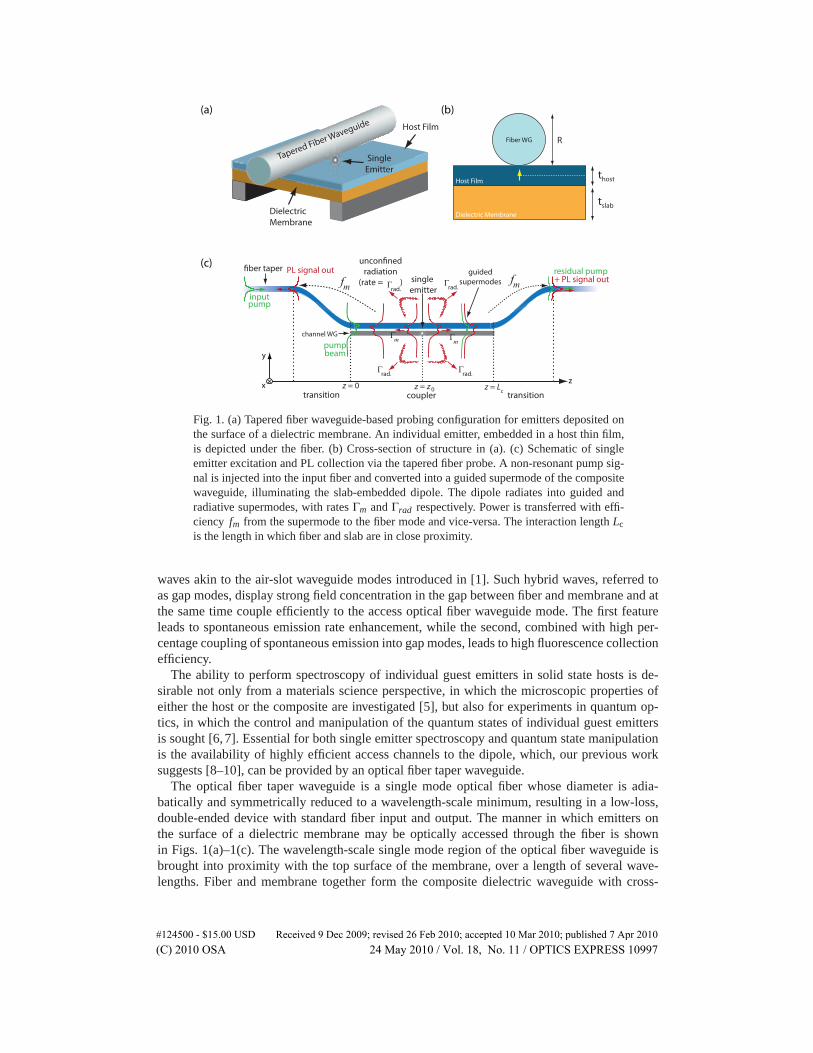
Fig. 1. (a) Tapered fiber waveguide-based probing configuration for emitters deposited onthe surface of a dielectric membrane. An individual emitter, embedded in a host thin film,is depicted under the fiber. (b) Cross-section of structure in (a). (c) Schematic of singleemitter excitation and PL collection via the tapered fiber probe. A non-resonant pump sig-nal is injected into the input fiber and converted into a guided supermode of the compositewaveguide, illuminating the slab-embedded dipole. The dipole radiates into guided andradiative supermodes, with rates Γm and Γrad respectively. Power is transferred with effi-ciency fm from the supermode to the fiber mode and vice-versa. The interaction length Lcis the length in which fiber and slab are in close proximity.
waves akin to the air-slot waveguide modes introduced in [1]. Such hybrid waves, referred toas gap modes, display strong field concentration in the gap between fiber and membrane and atthe same time couple efficiently to the access optical fiber waveguide mode. The first featureleads to spontaneous emission rate enhancement, while the second, combined with high per-centage coupling of spontaneous emission into gap modes, leads to high fluorescence collectionefficiency.
The ability to perform spectroscopy of individual guest emitters in solid state hosts is de-sirable not only from a materials science perspective, in which the microscopic properties ofeither the host or the composite are investigated [5], but also for experiments in quantum op-tics, in which the control and manipulation of the quantum states of individual guest emittersis sought [6, 7]. Essential for both single emitter spectroscopy and quantum state manipulationis the availability of highly efficient access channels to the dipole, which, our previous worksuggests [8–10], can be provided by an optical fiber taper waveguide.
The optical fiber taper waveguide is a single mode optical fiber whose diameter is adia-batically and symmetrically reduced to a wavelength-scale minimum, resulting in a low-loss,double-ended device with standard fiber input and output. The manner in which emitters onthe surface of a dielectric membrane may be optically accessed through the fiber is shownin Figs. 1(a)–1(c). The wavelength-scale single mode region of the optical fiber waveguide isbrought into proximity with the top surface of the membrane, over a length of several wave-lengths. Fiber and membrane together form the composite dielectric waveguide with cross-
#124500 - $15.00 USD Received 9 Dec 2009; revised 26 Feb 2010; accepted 10 Mar 2010; published 7 Apr 2010(C) 2010 OSA 24 May 2010 / Vol. 18, No. 11 / OPTICS EXPRESS 10997
section shown in Fig. 1(b), which supports a complete set of guided, leaky, and radiation super-modes originating from the hybridization of fiber and slab modes [11] (note that gap modes areindeed supermodes of the hybrid fiber-slab waveguide, as discussed in Section 4). As illustratedin Fig. 1(c), for non-resonant photoluminescence (PL) spectroscopy measurements, part of thenon-resonant pump power initially carried by the fiber is coupled to supermode waves thatreach the emitter. Illuminated by the pump, the emitter radiates (at a red-shifted wavelength)into supermodes of the composite waveguide, and a portion of the radiated power is outcou-pled through the two fiber ends. Using the same method, we also envision the possibility ofresonantly exciting the dipole, in which case the radiated fields (resonance fluorescence) wouldbe coherent and at the same wavelength as the pump signal. Backward-propagating resonancefluorescence can potentially be collected from the input fiber port by way of a directional cou-pler. In the forward direction, the power at the output fiber is given by the interference betweenthe excitation and resonant fluorescence signals, and may result in an enhanced or diminishedtransmission level [10, 12].
In [9], we analyzed the collection efficiency of the fiber taper waveguide for light emittedby a dipole embedded in a high refractive index membrane. We showed that the collection effi-ciency, achieved by tapping into emitted slab-confined waves, is potentially highly superior tothat attainable with standard free-space collection using high numerical aperture optics. Whilethe existence of the aforementioned gap modes was mentioned in that article, their potentialapplication in performing efficient spectroscopy of individual surface-bound dipoles was onlybriefly discussed, and not analyzed at any level of detail. Such an analysis is accomplished inthe following sections.
This paper is organized as follows. In Section 2, our simulation model and methods areexplained. In Section 3, simulation results of fluorescence collection for two configurationsappropriate for visible and infrared wavelengths are given. Section 4 analyzes the collectionefficiency results in terms of a hybrid waveguide mode decomposition. Parameters from thisanalysis are used in Section 5 to show the possibility of resonant field extinction by a singledipole. A discussion of the results follows in Section 6, and Section 7 concludes the paper.
2. Model and methods
We envision a general spectroscopy configuration for probing individual emitters in highlydilute guest-host material systems, examples of which are: colloidal quantum dots (CdSe,CdSe/ZnO, PbS, PbSe, etc) in polymer [13] or sol-gel [14] hosts; organic dyes in polymer [15]or small-molecule crystalline hosts [6, 16, 17]; rare-earth ions in transparent solid-state hosts[18]. In our configuration, a thin film of the guest-host material system would be producedon top of a dielectric, high refractive index material, chosen appropriately according to theguest emitter transition wavelength ranges. For instance, a Si (n ≈ 3.5) membrane could beused for near-infrared wavelengths above 1 μm, while SiNx (n ≈ 2.0) could be used for visi-ble light emission. We point out that such thin-film structures may be produced in most caseswith well-known, standard nanofabrication techniques. As depicted in Figs. 1(a) and 1(b), atapered optical fiber waveguide brought into contact with the host material provides both theexcitation and collection channels to the guest emitters. We analyze this structure with the samemethod as in [9], where single emitter collection efficiency from dipoles embedded in a dielec-tric membrane was studied. The simulation model and analysis methods are briefly describedbelow.
2.1. Simulation model
We model the problem as in Fig. 1(b). An individual electric point dipole embedded in a thinhost film on the surface of a dielectric membrane of thickness tslab and refractive index nslab
#124500 - $15.00 USD Received 9 Dec 2009; revised 26 Feb 2010; accepted 10 Mar 2010; published 7 Apr 2010(C) 2010 OSA 24 May 2010 / Vol. 18, No. 11 / OPTICS EXPRESS 10998
is probed by an optical fiber taper waveguide of radius R and index nfiber = 1.45. The dipole,oriented normal to the membrane surface, is assumed to be at the center of a dielectric hostfilm of index nhost and thickness thost. It is also assumed to be aligned with the center of theprobing fiber. As in Fig. 1(c), an excitation signal, resonant or non-resonant with one of theemitter’s transitions, is launched into the fiber input and adiabatically reduced in size as thefiber is tapered, exciting supermodes of the coupler structure. Supermodes with sufficient lateralconfinement illuminate the dipole, at a position z = z0 along the coupler. Under non-resonantexcitation, the dipole emits coupler supermodes in the ±z directions, at a red-shifted wave-length. The emitted supermodes are converted into input and output fiber modes through thetaper transition regions, after which emission is detected.
2.2. Fluorescence collection simulation
To estimate the PL collection efficiency of our fiber-based probing scheme, we simulated asingle classical electric dipole radiating in the composite dielectric waveguide of Fig. 1(a),using the Finite Difference Time Domain (FDTD) method [9]. The simulation provided thesteady-state fields over the entire computational window, which was cubic, with more than sixwavelengths in size. These were used to calculate an upper bound for the percentage of thetotal emitted power PTot. coupled to the fundamental optical fiber mode at an arbitrary positionz along the guide, with the expression
ηPL = 2Pz
PTot.ffiber. (1)
Here, Pz is the power flowing normally through the constant-z plane, ffiber is the overlap in-tegral in Eq. (2), taken between the radiated field at position z and the fundamental (isolated)fiber mode. The factor of 2 accounts for collection from both fiber ends. The symmetry of thegeometry allowed us to choose symmetric (x×H = 0) boundary conditions on the yz-plane, asonly y-polarized dipoles were considered. Perfectly-matched layers (PMLs) were used aroundthe domain limits to simulate an open domain. Simulations ran until no field amplitude couldbe detected in the domain. As in [9], ηPL oscillates with z, due to the back-and-forth power ex-change between the guide and the slab along the waveguide. The values of ηPL reported belowcorrespond to maxima obtained within the computational window.
2.3. Supermode analysis
We analyze the results from the FDTD simulations in terms of the supermodes supported bythe coupler structure formed by the fiber and slab. This provides us with insight into the col-lection mechanisms and ways to improve it, as well as the ability to determine the possibilityof observing extinction of resonant input signals by a single dipole. The formalism we employclosely follows that used in our previous work [9].
Supermode field profiles and the respective complex propagation constants βm are obtainedwith a finite-element based eigenvalue solver, with a vectorial formulation. Supermode m’s in-dividual contribution to the total PL collection efficiency ηPL, considering one fiber channel, isηPL,m = fm ·Γm/Γ = fm ·γm, where Γm is the supermode emission rate, and Γ the total emissionrate. The fraction γm is supermode m’s spontaneous emission coupling factor (β -factor), which,since emission in both ±z directions is equally likely, is such that 0 ≤ γm ≤ 0.5. The fiber modefraction, fm, is the percentage of supermode m’s power that is transferred to the output fibermode. Assuming that the fiber is abruptly removed from the slab at the end of the probing re-gion, and that reflections at the interface are small, fm may be approximated with an overlap
#124500 - $15.00 USD Received 9 Dec 2009; revised 26 Feb 2010; accepted 10 Mar 2010; published 7 Apr 2010(C) 2010 OSA 24 May 2010 / Vol. 18, No. 11 / OPTICS EXPRESS 10999
integral between the fundamental fiber mode and supermode m [19, 20]:
fm =Re
{∫∫S(e f ×h∗
m) · zdS∫∫
S(em ×h∗f ) · zdS
}
Re{∫∫
S(e f ×h∗f ) · zdS
}Re{∫∫
S(em ×h∗m) · zdS}
. (2)
In this expression, valid for purely dielectric waveguides, {em,hm} and{
e f ,h f}
are the super-mode and fundamental fiber mode fields, respectively. The supermode emission rates Γm is alsoobtained from the field profiles, according to the expressions given in [9].
We point out that most of the supermodes supported by the fiber and membrane structure areleaky [11], i.e., power confined in the area beneath the fiber leaks away from it as the supermodepropagates. The power leakage rate per propagation length is related to the imaginary part of thecalculated supermode’s complex effective index ne f f . The number of free-space wavelengthsnecessary for the supermode amplitude to decay by a factor 0 < δ < 1 is Nδ =−n−1
i ln(δ )/2π ,where n−1
i = Im{neff}−1, and an effective supermode propagation length Leff,δ = Nδ λ may bedefined.
2.4. Field Extinction
For coherent, resonant excitation, the power detected at the output fiber port is a result of the in-terference between the excitation signal and the resonance fluorescence from the emitter (whichare at the same wavelength), and may be either higher or lower than the detected power in theabsence of the dipole. In order to determine the variation in the transmitted power level dueto the presence of a single dipole, we make use of the quantum optics input-output formalismof [21], with which we obtain operators for the multimode field for z > z0, i.e., past the dipolelocation:
E(+)(z, t) = i√
2π ∑m
√hω
4πSmeme−i(ωt−βmz) ×
×[am
in(t −nmz/c)+√
Γm∗σ−(t −nmz/c)
]. (3)
Here, σ− is the atomic lowering operator, amin is (incident) supermode m’s input field annihi-
lation operator, em is the electric field distribution, βm the propagation constant, nm the phaseindex, and Sm = Re{∫S dS(em ×h∗
m) · z}, with S the xy plane. The expression in brackets is awell-known result of the input-output formalism, with explicit input (or ”free”) fields and ra-diated (”source”) contributions [21], expanded in terms of supermodes. The field operators arethen inserted in the fiber mode power operator [10],
F ={∫
SdS(E(−) ×h f ) · z
∫
SdS(e∗f ×H(+)) · z+
∫
SdS(H(−) × e f ) · z
∫
SdS(h∗
f ×E(+)) · z}
S−1f , (4)
where e f and h f are the fiber mode electric and magnetic field distributions, Sf =Re{∫S dS(e f × h∗
f ) · z}. In short, the fiber mode power operator allows us to determine thetotal photon flux coupled into the output fiber mode, based on multimode field operators thatdescribe the coherent interference between the incident (’free’) and emitted, resonance fluores-cence (’source’) supermode waves; the operator is the quantum optics equivalent to the overlapintegral in Eq. (2), between the total field at a position z along the waveguide and the opti-cal fiber mode. This corresponds to the power coupled into the output fiber at the end of the
#124500 - $15.00 USD Received 9 Dec 2009; revised 26 Feb 2010; accepted 10 Mar 2010; published 7 Apr 2010(C) 2010 OSA 24 May 2010 / Vol. 18, No. 11 / OPTICS EXPRESS 11000
coupling region, assuming an abrupt transition and small reflections at the interface [19]. Con-sidering coherent, steady-state, multimode field excitation, the photon flux F at the output fiber(normalized to the input field power) is found to be
F = hωRe
{
∑m,m′
√fm
√fm′ei(βm′−βm)(z−z0) × (5)
×[
BmB∗m′ +
√Γm
√Γm′ ∗ζ − Γ
2
(B∗
m√
Γm′ ∗ξ +Bm′√
Γmξ ∗)
(Γ2
)2 +2ζ
]}
,
with ξ = ∑m
√ΓmBm, ζ = ∑
m,m′Re
{√Γm
√Γm′
∗B∗
mBm′}
. In this expression, Bm is the complex
amplitude of the m-th supermode incident on the dipole. The magnitude of Bm is determined bythe manner with which the fiber is brought into contact with the slab. For instance, for abruptcontact (e.g., very short transition regions in Fig. 1), it approaches | fm|1/2, where fm is the fiber-mode fraction. Longer transition regions could lead to a power distribution among the excitedsupermodes different from that obtained with the fiber-mode fractions. The phase of the Bm
coefficients at the dipole position is determined through the supermode propagation constantsβm, assuming all modes are in-phase at the start of the coupler region.
To gain some insight into the mechanisms at play at resonant excitation, we consider a situ-ation in which only one supermode of the fiber and slab structure may be accessed: in Eq. (5),we set all fiber-mode fractions fm and incident supermode amplitudes Bm to be null except forthose of an arbitrary M-th supermode (i.e., fm=M = 0, Bm=M = 0). We furthermore make theassumption that the excitation signal drives the transition far from saturation, so that ζ/Γ2 1and the denominator of the second term in brackets becomes unity. In this case, the power de-tected at the output fiber is proportional to 1−4γM(1−γM). Thus the magnitude of optical fieldextinction by a single dipole is determined by the supermode spontaneous emission couplingfactor, and is complete when γM = 0.5.
3. Fluorescence Collection Efficiency
Two configurations were analyzed, for operation at visible (λ = 600 nm) and near-infrared(λ = 1300 nm) wavelengths. For the visible range, a 130 nm thick SiN membrane (refractiveindex nSiN = 2.0) and 400 nm diameter single mode fiber taper waveguide were considered. Inthe near-infrared case, our model consists of a 160 nm thick Si membrane (refractive index nSi =3.505) and a 1 μm diameter fiber taper, which supports a well-confined and a near-cutoff mode.The first configuration models a system suitable for probing visible wavelength emitters suchas single molecules or CdTe/ZnSe nanocrystal quantum dots attached to the SiN membrane,while the second would be suitable for infrared emitters, such as PbS and PbSe nanocrystalquantum dots [22]. In both cases, the emitters are considered to be embedded in a 20 nm thick,purely dielectric host film on top of the SiN or Si membranes, as shown in Fig. 1(b). The hostfilm refractive index nhost is allowed to vary between 1.0 and 1.7, a range that includes typicalvalues for possible organic (e.g., PMMA) or inorganic (e.g., silica) transparent host materials.The emitters are modeled as electric dipoles oriented in the y-direction. While this considerationlimits our analysis to a best-case scenario for emitters with random dipole orientation, it maybe well suited to model certain organic crystal guest-host systems, where emitting moleculesembedded in the host crystal tend to align in specific orientations. For instance, in the guest-hostsystem presented in [23], consisting of Terrylene molecules in a crystalline p-terphenyl host -asystem fit for molecular quantum optics [6]-, the guest molecules have been shown to displaydipole moments perpendicularly oriented to the substrate.
#124500 - $15.00 USD Received 9 Dec 2009; revised 26 Feb 2010; accepted 10 Mar 2010; published 7 Apr 2010(C) 2010 OSA 24 May 2010 / Vol. 18, No. 11 / OPTICS EXPRESS 11001
1 1.2 1.4 1.6 1.818
19
20
21
22
23
24
nhost
η PL (%
)
SiNx, λ = 600 nmSi , λ = 1300 nm
1 1.2 1.4 1.6 1.80
5
10
15
20
nhost
Γ / Γ
hom.
SiN, λ= 600 nmSi, λ = 1300 nm
(a) (b)
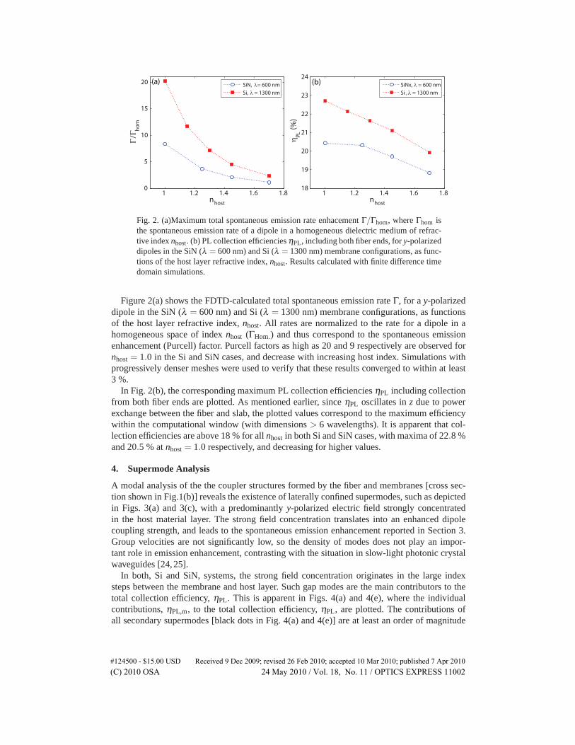
Fig. 2. (a)Maximum total spontaneous emission rate enhacement Γ/Γhom, where Γhom isthe spontaneous emission rate of a dipole in a homogeneous dielectric medium of refrac-tive index nhost. (b) PL collection efficiencies ηPL, including both fiber ends, for y-polarizeddipoles in the SiN (λ = 600 nm) and Si (λ = 1300 nm) membrane configurations, as func-tions of the host layer refractive index, nhost. Results calculated with finite difference timedomain simulations.
Figure 2(a) shows the FDTD-calculated total spontaneous emission rate Γ, for a y-polarizeddipole in the SiN (λ = 600 nm) and Si (λ = 1300 nm) membrane configurations, as functionsof the host layer refractive index, nhost. All rates are normalized to the rate for a dipole in ahomogeneous space of index nhost (ΓHom.) and thus correspond to the spontaneous emissionenhancement (Purcell) factor. Purcell factors as high as 20 and 9 respectively are observed fornhost = 1.0 in the Si and SiN cases, and decrease with increasing host index. Simulations withprogressively denser meshes were used to verify that these results converged to within at least3 %.
In Fig. 2(b), the corresponding maximum PL collection efficiencies ηPL including collectionfrom both fiber ends are plotted. As mentioned earlier, since ηPL oscillates in z due to powerexchange between the fiber and slab, the plotted values correspond to the maximum efficiencywithin the computational window (with dimensions > 6 wavelengths). It is apparent that col-lection efficiencies are above 18 % for all nhost in both Si and SiN cases, with maxima of 22.8 %and 20.5 % at nhost = 1.0 respectively, and decreasing for higher values.
4. Supermode Analysis
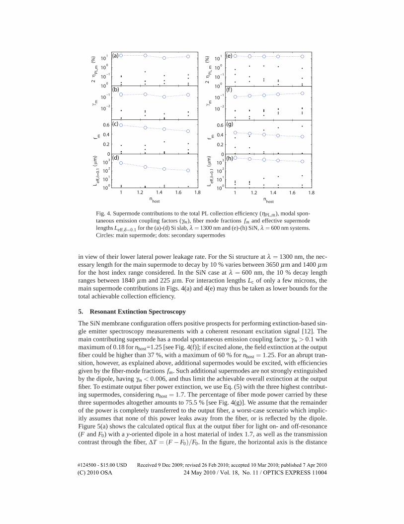
A modal analysis of the the coupler structures formed by the fiber and membranes [cross sec-tion shown in Fig.1(b)] reveals the existence of laterally confined supermodes, such as depictedin Figs. 3(a) and 3(c), with a predominantly y-polarized electric field strongly concentratedin the host material layer. The strong field concentration translates into an enhanced dipolecoupling strength, and leads to the spontaneous emission enhancement reported in Section 3.Group velocities are not significantly low, so the density of modes does not play an impor-tant role in emission enhancement, contrasting with the situation in slow-light photonic crystalwaveguides [24, 25].
In both, Si and SiN, systems, the strong field concentration originates in the large indexsteps between the membrane and host layer. Such gap modes are the main contributors to thetotal collection efficiency, ηPL. This is apparent in Figs. 4(a) and 4(e), where the individualcontributions, ηPL,m, to the total collection efficiency, ηPL, are plotted. The contributions ofall secondary supermodes [black dots in Fig. 4(a) and 4(e)] are at least an order of magnitude
#124500 - $15.00 USD Received 9 Dec 2009; revised 26 Feb 2010; accepted 10 Mar 2010; published 7 Apr 2010(C) 2010 OSA 24 May 2010 / Vol. 18, No. 11 / OPTICS EXPRESS 11002
x ( μm)
y (μ
m)
−1 −0.5 0 0.5 1
−1
−0.5
0
0.5
1
0.20.40.60.8
0 0.5 1|E
y|/|E
max|
|Ey|/
|Em
ax|
x ( μm)
y (μ
m)
|Ey|/
|Em
ax|
−1 −0.5 0 0.5 1
−1
−0.5
0
0.5
1
0.20.40.60.8
0 0.5 1|E
y|/|E
max|
x ( μm)
y (μ
m)
−0.5 0 0.5
−0.4
0
0.4
0.8
0.20.40.60.8
0 0.5 1|E
y|/|E
max|
|Ey|/
|Em
ax|
x ( μm)
y (μ
m)
−0.5 0 0.5
−0.4
0
0.4
0.8
0.20.40.60.8
0 0.5 1|E
y|/|E
max|
|Ey|/
|Em
ax|
(a)
(c) (d)
(b)
λ = 1300 nm λ = 1300 nm
λ = 600 nm λ = 600 nm
t = 130 nmslab
t = 160 nmslab
n = 3.505slab
n = 2.0slab
t = 130 nmslab
n = 2.0slab
t = 160 nmslab
n = 3.505slab
n = 1.0host n = 1.7host
n = 1.0host n = 1.7host
Fig. 3. Amplitude of the major electric field component (Ey) of laterally bound gap modes(normalized to the maximum electric field amplitude, |E|max) for the (a), (b) Si slab config-uration (λ = 1300 nm) with (a) nhost = 1.0 and (b) nhost = 1.7; (c), (d) SiN configuration(λ = 600 nm) with (c) nhost = 1.0 and (d) nhost = 1.7. In all cases, thost = 20 nm. Line plotsshow |Ey|/|E|max on the x = 0 plane (dotted line in the contour plots).
smaller than the main ones. Despite providing small individual contributions, secondary super-modes altogether make up for a large portion of the total collected power. It is important tonote that, even though many of the secondary supermodes are indeed gap modes, poor lateralconfinement causes these to exhibit large effective areas, and therefore low emission rates Γm.Correspondingly, low emission coupling factors γm (γm = Γm/Γ, with Γ the total spontaneousemission rate) are observed in Figs. 4(b) and 4(f). For the main modes, γm > 10 %, so these gapmodes carry a considerable percentage of the total spontaneous emission.
The oscillation of the total efficiency ηPL as a function of z, mentioned in Section 3, canbe traced to the beating of the two main contributing supermodes. The beat length is givenby Lz = 2π/(Δβ ), where Δβ is the difference between the propagation constants. For the Si,λ = 1.3 μm configuration, the beat length varies between 4.78 μm, for nhost = 1.0 and 3.89 μm,for nhost = 1.7. In the SiN, λ = 0.6 μm case, it varies between 2.72 μm, for nhost = 1.0 and2.17 μm, for nhost = 1.7. In order to maximize the collected power, therefore, control of theinteraction length Lc on the scale a few microns is desirable.
At the same time, short interaction lengths Lc are desirable because all supermodes exhibitsome degree of lateral power leakage due to imperfect field confinement. Figures 4(d) and 4(h)show the effective lengths Leff,δ , defined in Section 2.3, necessary for 10 % supermode am-plitude decay, for the Si and SiN case respectively. It is apparent that in both cases the mainsupermodes have considerably longer (more than two decades) effective lengths, as expected,
#124500 - $15.00 USD Received 9 Dec 2009; revised 26 Feb 2010; accepted 10 Mar 2010; published 7 Apr 2010(C) 2010 OSA 24 May 2010 / Vol. 18, No. 11 / OPTICS EXPRESS 11003
10−2
10−1
100
γ m
10−1
100
101
2 η
PL,m
(%)
0
0.2
0.4
0.6
nhost
f m
1 1.2 1.4 1.6 1.810
0
101
102
103
nhost
L eff,δ
=0.
1 (
μm)
10−2
10−1
100
γ m
10−1
100
101
2 η
PL, m
(%)
0
0.2
0.4
0.6
nhost
f m
1 1.2 1.4 1.6 1.810
0
101
102
103
nhost
L eff,δ
=0.
1 (
μm)
(a)
(b)
(c)
(d)
(e)
(f )
(g)
(h)
Fig. 4. Supermode contributions to the total PL collection efficiency (ηPL,m), modal spon-taneous emission coupling factors (γm), fiber mode fractions fm and effective supermodelengths Leff,δ=0.1 for the (a)-(d) Si slab, λ = 1300 nm and (e)-(h) SiN, λ = 600 nm systems.Circles: main supermode; dots: secondary supermodes
in view of their lower lateral power leakage rate. For the Si structure at λ = 1300 nm, the nec-essary length for the main supermode to decay by 10 % varies between 3650 μm and 1400 μmfor the host index range considered. In the SiN case at λ = 600 nm, the 10 % decay lengthranges between 1840 μm and 225 μm. For interaction lengths Lc of only a few microns, themain supermode contributions in Figs. 4(a) and 4(e) may thus be taken as lower bounds for thetotal achievable collection efficiency.
5. Resonant Extinction Spectroscopy
The SiN membrane configuration offers positive prospects for performing extinction-based sin-gle emitter spectroscopy measurements with a coherent resonant excitation signal [12]. Themain contributing supermode has a modal spontaneous emission coupling factor γm > 0.1 withmaximum of 0.18 for nhost=1.25 [see Fig. 4(f)]; if excited alone, the field extinction at the outputfiber could be higher than 37 %, with a maximum of 60 % for nhost = 1.25. For an abrupt tran-sition, however, as explained above, additional supermodes would be excited, with efficienciesgiven by the fiber-mode fractions fm. Such additional supermodes are not strongly extinguishedby the dipole, having γm < 0.006, and thus limit the achievable overall extinction at the outputfiber. To estimate output fiber power extinction, we use Eq. (5) with the three highest contribut-ing supermodes, considering nhost = 1.7. The percentage of fiber mode power carried by thesethree supermodes altogether amounts to 75.5 % [see Fig. 4(g)]. We assume that the remainderof the power is completely transferred to the output fiber, a worst-case scenario which implic-itly assumes that none of this power leaks away from the fiber, or is reflected by the dipole.Figure 5(a) shows the calculated optical flux at the output fiber for light on- and off-resonance(F and F0) with a y-oriented dipole in a host material of index 1.7, as well as the transmissioncontrast through the fiber, ΔT = (F −F0)/F0. In the figure, the horizontal axis is the distance
#124500 - $15.00 USD Received 9 Dec 2009; revised 26 Feb 2010; accepted 10 Mar 2010; published 7 Apr 2010(C) 2010 OSA 24 May 2010 / Vol. 18, No. 11 / OPTICS EXPRESS 11004
from the dipole to the end of the coupler region, as indicated in Fig. 1, and z0 = 1 μm. Theoscillations in F , F0 and ΔT along z evidence the back-and-forth power transfer between fiberand slab, and the amplitude decay is indicative of both the interference and leaky nature of thesupermodes involved. It is apparent that, for z− z0 � 0, the extinction level may reach ≈ 20 %.
5 10 15 20 25 30 35 40 450
0.2
0.4
0.6
0.8
1
F, F
0
z−z0
(μm)5 10 15 20 25 30 35 40 45
−1
−0.8
−0.6
−0.4
−0.2
0
ΔT
F
F0
ΔT
1 1.1 1.2 1.3 1.4 1.5 1.6 1.7−1
−0.9
−0.8
−0.7
−0.6
−0.5
−0.4
−0.3
−0.2
−0.1
0
nhost
Δ T
Single mode
Multimode
(a) (b)
Fig. 5. (a) Normalized, off- and on-resonance transmission (F0 and F) and contrast ΔT =(F −F0)/F0 as functions of separation from a single, y-oriented dipole at z0. The dipole isembedded in a host material with nhost = 1.7 on top of a 130 nm thick SiN membrane, andemits at λ = 600 nm. (b) Achievable transmission contrast ΔT as a function of the host filmindex nhost. Squares: results obtained assuming dipole excitation with the main supermodeonly; circles: assuming multimode excitation (see text for details).
Figure 5(b) shows the achievable extinction ratio at z− z0 = 50 μm, under the same assump-tions, for all host indices considered (circles). We also plot the extinction levels achievable un-der the single supermode assumption (squares), which makes explicit the degradation of extinc-tion due to the excitation of additional supermode waves. The highest achievable extinction maybe as much as 34 % for nhost = 1.0, for which the Purcell enhancement is maximum and consid-erably stronger than for nhost = 1.7. This result suggests that, as long as the input signal poweris sufficiently below the transition saturation power, the Purcell effect does not influence theachievable extinction level. This is to be expected, given that the aforementioned expressionfor extinction in the case of single mode excitation and collection, F ∼ 1− 4γm(1− γm), onlydepends on the modal spontaneous coupling factor γm. Purcell enhancement will influence thepower at which dipole saturation occurs, and may thus have implications in obtaining betterdetection signal-to-noise ratios.
Similar performance may in principle be achieved with the Si system, for an appropriate setof parameters. The situation, however, is less favorable for the parameters considered here: inFig. 4(c), for nhost > 1.2, the main supermode fiber fraction is surpassed by that of the secondmode, which is only weakly affected by the dipole [γm < 0.01 in Fig. 4(b)]. Assuming thatthe second supermode is completely transmitted, that 40 % of the power in the fiber is carriedby the main supermode [see Fig. 4(c)], and that the latter is extinguished by 31 % [γm = 0.22,Fig. 4(b)], the maximum achievable overall extinction would be only 12 %. Although lower thanin the SiN cases studied above, such an extinction level is still quite reasonable for spectroscopypurposes, and is compatible with experimentally observed levels using an NSOM tip [12] anda solid immersion lens [26].
#124500 - $15.00 USD Received 9 Dec 2009; revised 26 Feb 2010; accepted 10 Mar 2010; published 7 Apr 2010(C) 2010 OSA 24 May 2010 / Vol. 18, No. 11 / OPTICS EXPRESS 11005
6. Discussion
In slot waveguides consisting of two high refractive index channels separated by a small gap [1],strong field concentration in the gap results from the continuity of the normal electric displace-ment vector component at dielectric interfaces, with the field concentration increasing for in-creasing refractive index discontinuity. This behavior is evident in Figs. 3(a), 3(b) and 3(c), 3(d),which depict the intensity of the electric field in the host region, for host film refractive in-dices nhost = 1.0 and nhost = 1.7, for both the Si and SiN configurations. The decrease in fieldconcentration for larger indices is apparent in the Purcell factor decrease for increasing hostmaterial index nhost [Fig. 2(b)]. However, even in situations where the Purcell factor is small,gap supermodes have relatively high modal spontaneous emission coupling factors (γm) and ef-ficient coupling to the fiber mode ( fm) (see Fig. 4), which creates the conditions for performingextinction-type, resonant spectroscopy on individual emitters.
We point out that the cases in which the highest Purcell enhancements are observed, in whichnhost = 1.0, would be challenging or not achievable in practice. These situations, which other-wise provide upper bounds for the achievable enhancement, imply the absence of a host materialsupporting the emitter, or, in the best case, the ability to produce a 20 nm thick host layer ofextremely low refractive index material, for instance an aerogel. It is also worthwhile notingthat, although semiconductor nanocrystal quantum dots are composed of high refractive indexmaterials, sufficiently small nanocrystals may not constitute a significant disturbance to the en-vironment, that could lead to large deviations from our calculated results. Evidence of this canbe found in [27], where small (< 5 nm) PbS nanocrystal quantum dots were shown to not con-siderably affect the modes of a high quality factor microresonator. A similar conclusion may bedrawn from the simulations involving diamond nanocrystals in nanocavities reported in [28].
We reiterate that the results presented here are best-case estimates, obtained for verticaldipole moments aligned with the gap mode field. Horizontal dipole moments are expected to ra-diate at lower rates. In the case of z-dipoles, gap waves are generated at lower rates because thedipole moment is aligned with the minor supermode field component, Ez. If located at the x = 0plane, an x-dipole is completely uncoupled from gap modes, producing, rather, anti-symmetric(y×E|x=0=0) supermode waves with a major x-field component. These do not offer the samestrong field concentration as gap modes, due to the continuity of the electric field across thegap.
As in the situation studied in [9], relating to PL collection from slab-embedded dipoles, lat-eral modal confinement plays an important role. Despite the high γm factors of the main gapsupermodes, a significant portion of the dipole power is emitted into supermodes with very poorlateral confinement, which in a short distance along z propagate away from the fiber and are notcollected. Thus, the length of the interaction region must be minimized for a maximized collec-tion. In addition, enforcing strong lateral confinement via the formation of a channel, rather thana membrane, may significantly enhance collection efficiency. For instance, by replacing the SiNmembrane studied above with a channel waveguide of the same thickness, but with a width of600 nm and with a host material of index nhost = 1.45, a collection efficiency of ≈ 49 % may beachieved with a Purcell factor of ≈ 2. Additionally, as in [10], a channel waveguide structuremay also benefit resonant excitation experiments, not only with an enhanced resonance fluores-cence collection efficiency, but also with higher extinction levels, or even enhancement of theoutput power relative to the transmission level without the dipole. In this case, tapered fiber andchannel waveguides may be designed to form a phase-matched directional coupler, with highγm supermodes. The waveguide could furthermore be designed to allow efficient power transferfrom the fiber to a single supermode, so that the single-mode situation mentioned in Section 5may be achieved. In this case, provided the single supermode’s γm is large, high field extinctionmay be achieved independent of the coupler length or emitter position along its length [10].
#124500 - $15.00 USD Received 9 Dec 2009; revised 26 Feb 2010; accepted 10 Mar 2010; published 7 Apr 2010(C) 2010 OSA 24 May 2010 / Vol. 18, No. 11 / OPTICS EXPRESS 11006
For the channel waveguide situation just described, γm = 0.215 for the main supermode, whichwould lead to a single-mode extinction of 67 %.
Finally, we point out that the recently reported plasmonic laser [29], composed of a cylindri-cal CdS nanowire placed on top of a Ag substrate, with a thin MgS separator [the cross sectionclosely resembles that in Fig. 1(b)] supports gap modes similar to those studied here. Whilehere the supermodes are hybrids of fiber and slab modes, those in [29] are hybrids of the cylin-der and surface plasmon modes. Although hybrid plasmonic waveguides offer substantiallystronger Purcell enhancement for emitters located in the MgS spacer or in the nanowire, thesupermodes suffer from high propagation losses associated with the surface plasmon. Indeed,supermode propagation lengths (i.e., the required length for the mode power to drop in half)quoted in [29] are on the order of 10 wavelengths. In the present case, supermode effectivelengths are two to three orders of magnitude longer, since the waveguides are purely dielectric,and lateral power leakage is small.
7. Conclusions
We have performed detailed electromagnetic simulations that indicate that a tapered opticalfiber waveguide may be an efficient photoluminescence collection probe for individual dipolesplaced on the surface of dielectric membranes. High maximum collection efficiencies (> 20 %)are predicted, and are related to hybrid supermodes of the composite fiber-slab structure, whichpresent strong field concentration in the gap between slab and fiber. These supermodes are akinto the gap modes supported by slotted waveguides [1]. Our results also indicate that this probingconfiguration may be used to perform resonant spectroscopy of single emitters on membranesurfaces, and we predict that an extinction of at least 20 % of a fiber-coupled resonant excitationsignal is achievable.
Acknowledgement
This work has been supported in part by the NIST-CNST/UMD-NanoCenter CooperativeAgreement.
#124500 - $15.00 USD Received 9 Dec 2009; revised 26 Feb 2010; accepted 10 Mar 2010; published 7 Apr 2010(C) 2010 OSA 24 May 2010 / Vol. 18, No. 11 / OPTICS EXPRESS 11007