Product labels Features • Externally programmable VBUS OVP (over voltage protection) and OCP (over current protection) for provider and consumer power paths with fast turn-off • Two integrated N-MOSFETs gate drivers for VBUS OVP and OCP • Very low power in “unattached” state during DRP toggling: 3 µA max. at 125 °C • Compliant with PPS (programmable power supply) for fast charging, up to 100 W • Integrated discharge on VBUS and VCONN • VBUS current sense and amplifier with analog output • ESD protection for CC1, CC2, compliant with IEC 61000-4-2 Level 4 (±8 kV contact discharge, ±15 kV air discharge) • V CONN OCP (100 mW max), OVP (6 V max) • Over voltage protection on CC lines against short-to-V BUS • Over temperature protection (150 °C typ.) • Integrated “Dead Battery” management • I 2 C communication, with two I 2 C addresses available • Junction temperature from -40 °C to 125 °C • Compliant with USB-C power delivery standard 3.1, standard power range (SPR), up to 100 W • ECOPACK2 compliant Applications • USB type-C power delivery used in dual role power (DRP) or dual role data (DRD) configuration • USB type-C used in Sink configuration requiring current sense on V BUS • USB type-C sourcing devices Description The TCPP03-M20 is an MCU companion chip enabling cost-effective USB-C power delivery dual role power implementation. It provides protections and functionalities to safely comply with the USB-C Power Delivery specification. TCPP03-M20 drives external N-MOSFETs on VBUS connector pin in the source and sink power path for over voltage and over current protection. It provides an analog current sense output accessible for an MCU ADC, thus minimizing system cost. The TCPP03-M20 features 24 V tolerant ESD protection as per IEC61000-4-2 level 4 on USB type-C connector communication channel pins (CC). The TCPP03-M20 provides overvoltage protection on CC1 and CC2 pins when these pins are subjected to short circuit with the VBUS pin that may happen when removing the USB type-C cable from its receptacle. TCPP03-M20 helps to minimize power consumption during DRP toggling states thanks to its three programmable power modes allowing a power consumption as low as 3 µA maximum, up to 125 °C and thanks to enable pin that wake up the MCU. Product status link TCPP03-M20 Order TCPP03-M20 Expansion board X-NUCLEO-DRP1M1 Software example code X-CUBE-TCPP STM32-UCPD companion chips (1) STM32G0, STM32G4, STM32L5, STM32U5 1. Any MCU with USB-C PD SW stack I2C address 0110 10x (LSB = ‘x’) USB-C protection for dual role power (DRP) TCPP03-M20 Datasheet DS13618 - Rev 2 - October 2021 For further information contact your local STMicroelectronics sales office. www.st.com
Transcript
Product labels
Features• Externally programmable VBUS OVP (over voltage protection) and OCP (over
current protection) for provider and consumer power paths with fast turn-off• Two integrated N-MOSFETs gate drivers for VBUS OVP and OCP• Very low power in “unattached” state during DRP toggling: 3 µA max. at 125 °C• Compliant with PPS (programmable power supply) for fast charging, up to
100 W• Integrated discharge on VBUS and VCONN• VBUS current sense and amplifier with analog output• ESD protection for CC1, CC2, compliant with IEC 61000-4-2 Level 4 (±8 kV
contact discharge, ±15 kV air discharge)• VCONN OCP (100 mW max), OVP (6 V max)• Over voltage protection on CC lines against short-to-VBUS
• Over temperature protection (150 °C typ.)• Integrated “Dead Battery” management• I2C communication, with two I2C addresses available• Junction temperature from -40 °C to 125 °C• Compliant with USB-C power delivery standard 3.1, standard power range
(SPR), up to 100 W• ECOPACK2 compliant
Applications• USB type-C power delivery used in dual role power (DRP) or dual role data
(DRD) configuration• USB type-C used in Sink configuration requiring current sense on VBUS
• USB type-C sourcing devices
DescriptionThe TCPP03-M20 is an MCU companion chip enabling cost-effective USB-C powerdelivery dual role power implementation. It provides protections and functionalities tosafely comply with the USB-C Power Delivery specification.
TCPP03-M20 drives external N-MOSFETs on VBUS connector pin in the source andsink power path for over voltage and over current protection. It provides an analogcurrent sense output accessible for an MCU ADC, thus minimizing system cost.
The TCPP03-M20 features 24 V tolerant ESD protection as per IEC61000-4-2 level4 on USB type-C connector communication channel pins (CC). The TCPP03-M20provides overvoltage protection on CC1 and CC2 pins when these pins are subjectedto short circuit with the VBUS pin that may happen when removing the USB type-Ccable from its receptacle.
TCPP03-M20 helps to minimize power consumption during DRP toggling statesthanks to its three programmable power modes allowing a power consumption aslow as 3 µA maximum, up to 125 °C and thanks to enable pin that wake up the MCU.
Product status link
TCPP03-M20
Order TCPP03-M20
Expansion board
X-NUCLEO-DRP1M1
Software example code
X-CUBE-TCPP
STM32-UCPD companion chips(1)
STM32G0, STM32G4, STM32L5,
STM32U5
1. Any MCU with USB-C PD SW stack
I2C address
0110 10x (LSB = ‘x’)
USB-C protection for dual role power (DRP)
TCPP03-M20
Datasheet
DS13618 - Rev 2 - October 2021For further information contact your local STMicroelectronics sales office.
Note: * UCPD stands for USB Type-C and Power Delivery
VCC IO ring (3.3 V ±10% -5 V ±10%)VddlO ring (1.8 V ±5% -3.3 V ±10%)
Battery
PowerManagement
Note: UCPD stands for USB type-C and power delivery interface.External components are described in Section 8.1 External components description.Please refer to TA0357 for an overview of USB type-C and power delivery technologies.Please refer to AN5225 for more informations related to USB type-C power delivery using STM32xx Series MCUsand STM32xxx series MPUs.For more information on EMI filtering and ESD protection of USB datalines, please refer to AN4871: USB type-Cprotection and filtering.
4.1 Parameter conditionsUnless otherwise specified:• All voltages are referenced to GND• The minimum and maximum values are guaranteed in the worst conditions of operating temperature, supply
voltage and frequencies, by tests in production on 100 % of the devices• Typical values are given only as design guidelines and are not tested• All typical curves are given only as design guidelines and are not tested
4.2 Absolute maximum ratingsStresses above the absolute maximum ratings listed in the tables below, may cause permanent damage to thedevice. These are stress ratings only and functional operation of the device at these conditions is not implied.Exposure to maximum rating conditions for extended periods may affect device reliability.
Table 2. Absolute maximum ratings (across junction temperature range)
Symbol Parameter Pin name Value Unit
VPOWER Voltage for power pins VCC_VCONN 7 VDC
VIN Voltage for input pinsEN, Vsense, I2C_ADD 7
VDCVBUSc, Isense, GDPs, GDCs 24
VOUT Voltage for output pinsIANA, FLGn 7 VDC
CBIAS, GDPg, GDCg 24
VI/O Voltage for input, output pinsSDA,SCL, CC1,CC2 7
VDCCC1c,CC2c 24
Rthj-a Junction to ambient thermal resistance 150 °C/W
TJ Junction temperature range -40 to +125 °C
TSTG Storage temperature range -55 to +150 °C
Table 3. ESD ratings (across junction temperature range)
Symbol Description Pins Value Unit
VESD_c
System level ESD robustness on USB Type-C connector side(1)
IEC61000-4-2 Level 4, contact discharge
IEC61000-4-2 Level 4, air discharge
CC1c, CC2c 8
15
kV
VHBM VESD ratings human body model (JESD22-A114D, level 2) All pins 2 kV
1. Internal ESD protection functionality is associated with external capacitor connected on pin CBIAS.
Note: for more information on IEC61000-4-2 standard testing, please refer to AN3353.
Table 4. Recommended operating condition, across junction temperature range
Pin name Min. Typ. Max. Unit
VCC_VCONN, CC1,CC2, VSENSE
2.7 5.5 V
EN, IANA, I2C_ADD,SDA, SCL, FLGn 1.7 3.6 V
CC1c, CC2c, VBUSc,ISENSE, GDPs, GDCs 0 22 V
4.4 Power supply (VCC_VCONN, VBUSc)
Table 5. Electrical characteristics – Power supply (VCC_VCONN, VBUSc) across Tj
Symbol Parameter Test condition across TOPValue
UnitMin. Typ. Max.
ICC_VCONN Vcc supply currentNormal mode - 2.7 mA
Low power mode - 1 µA
Ienable Supply current of EN pinLow power mode 1,7 V-2,7 V - 3 µA
Low power mode 2,7 V-3,6 V - 10 µA
IL_VBUSc VBUSc Supply currentVBUSc = 22 V - 2
mAVBUSc = 5 V - 0.7
TDIS_VBUSc VBUSc discharge time(1) - 220 ms
1. Equivalent discharge resistor is 2.5 kΩ typical.
4.5 VBUS OVP, OCP
Table 6. Electrical characteristics for VBUS (OVP, OCP, gate driver, current monitoring) across Tj
Symbol Parameter Test condition across TOPValue
UnitMin. Typ. Max.
VBUS_UVLO VBUS under voltage lock out 1.9 2.4 2.9 V
VGS Gate to source voltage consumer VBUSc = 5 V - 20 V 4.5 5 5.5 V
VOVP_TH OVP VBUS threshold voltage Vsense pin voltage 1.1 1.16 1.25 V
TOVP_ON_VBUS OVP VBUS turn-on time 95 145 ns
VTH_OCP_VBUS VBUS OCP threshold voltage Across sense resistor Rs 35 42 45 mV
TOFF_OCP_VBUS VBUS OCP response time 3 8 µs
Iana_gain Current sensing gain 39 42 45 V/V
VIANA IANA pin output voltage during OCP event on VBUS line 1.7 1.95 V
TON VBUS turn-on time 1 3 ms
TCPP03-M20Recommended operating conditions
DS13618 - Rev 2 page 6/33
4.6 CC lines OVP and ESD
Table 7. Electrical characteristics: CC lines OVP (CC refers to CC1 and CC2) across Tj
Symbol Parameter Test condition across TOPValue
UnitMin. Typ. Max.
RON_CC ON resistance of CC OVP FETNormal mode 0.7 1.5
ΩLow power mode 8 17 28
CON_CCEquivalent ON capacitance of CCx line innormal mode 0 - 1.2 V, f = 400 kHz 40 60 100 pF
VTH_CC CC OVP threshold voltage 5.5 5.75 6 V
VMIN Minimum voltage on CC1c, CC2c Current on CC1c or CC2c < 60 µA 0.7 V
RDB DB resistor Measured at 400 µA on CC1c / CC2c 4.1 5.1 5.6 kΩ
TOVP_CC OVP response time on the CC pins 60 100 ns
BWCCx Bandwidth on CCx pins at -3dB and 0 - 1.2 V 10 MHz
Table 8. Typical clamping voltage on CC lines after IEC61000-4-2 ±8kV contact discharge
TCPP03-M20 andSTM32G071 ESD First peak VCL 30 ns
OFF +8 kV 9.2 V 3.3 V
OFF -8 kV -7.7 V -1.0 V
ON +8 kV 14.8 V 6.3 V
ON -8 kV -11.8 V -1.5 V
Note: Measurements are performed on X-NUCLEO-DRP1M1 board plugged on top of NUCLEO-G071RB. Ten ESDdischarge are applied on connector (CC1c and CC2c) and the voltage measurement is done on MCU side (CC1and CC2), STM32 still functional after the ESD discharge.
4.7 VCONN OCP, discharge
Table 9. Electrical characteristics VCONN switch (OCP, discharge) across Tj
Symbol Parameter Test condition across TOPValue
UnitMin. Typ. Max.
RON_VCONN ON resistance of VCONN FET 2.1 3 5.5 Ω
IVCONN Current thru VCONN FET max operating current VCONN = 3.0 V - 5.5 V 40 mA
6.1 OverviewThe TCPP03-M20 is a cost effective solution to protect microcontrollers featuring built-in USB-C power delivery(UCPD) controller or other low voltage power delivery controller. It is especially adapted to dual role power, dualrole data applications but also for sink applications requiring a current sense functionality.Please refer to TA0357 for an overview of USB type-C and power delivery technologies.Please refer to AN5225 for more informations related to USB type-C power delivery using STM32xx Series MCUsand STM32xxx series MPUs.
6.2 Power modesThe TCPP03-M20 embeds three distinct power modes controlled by the UCPD controller via the I2C bus.
Figure 8. Power modes process
Hibernate:• TCPP03 acts as a SINK in dead battery
mode
Low power:• Toggling between SOURCE & SINK
possible.• PD communication impracticable
Start-up
I2C command
Unattached State
I2C command
Attached State
No DC current on ENABLENo DC current on VCC_VCONN
Low DC current on ENABLENo DC current on VCC_VCONN
Normal DC current on ENABLENormal DC current on VCC_VCONNNormal:
1. Dynamic current of I2C interface have to be added to the values indicated when the I2C bus is used.2. ESD leakage current have to be added to the values indicated.3. For pin EN voltage between 1.7 V and 3.6 V.
Table 12. TCPP03-M20 states versus power modes
Powermode
CCswitches
OVPCC
Deadbatteries
Gatedriver
consumer
Gatedriver
provider
OVPVBUS FLGn I2C IANA
OCPVBUS
VCONNVBUSDis.
Comment
OFF OFF NA ON ON(1) OFF ON VBUSconnect OFF OFF OFF OFF TCPP not
powered
Hibernate OFF NA ON Controlledby I2C OFF ON VBUS
connect ON OFF OFF OFF Default stateat start-up
Lowpower
Highohmic
5 Vclamp OFF Controlled
by I2C OFF ON VBUSconnect ON OFF OFF OFF Signaling only
Normal Full perf. ActiveOVP OFF Controlled by I2C ON Failure
flags ON ON ON Controlledby I2C
PDcommunicationactive
1. Consumer (sink) gate driver is self biased with VBUSc voltage
TCPP03-M20Power modes
DS13618 - Rev 2 page 11/33
6.3 I2C registersThe I2C address used by TCPP03-M20 is 0110 10x, with LSB = ‘x’.The LSB bit of the I2C address is set when connecting TCPP03-M20 pin I2C_ADD to GND (for LSB = ‘0’) or to1.8 V or 3.3 V (for LSB = ’1’).
Figure 9. I2C registers
V2 V1VCONN switch
VC2 VC1
0 0 Open Open
1 0 OpenClose
0 1 CloseOpen
1 1 Open Open
V1V2Gate DriverProvider
(GDP)
GDP=1:• Switch load
closedGDP=0:• Switch load
opened
VBUSD=1:• VBUS
discharge ONVBUSD=0:• VBUS
discharge OFF
VBUS DISCHARGE
(VBUSD)
FLGn OCP_VCONN
FLGnOTP
FLGn OVP_VBUS
FLGn OCP_VBUS
Gate DriverConsumer
(GDC)
GDC=1:• Switch load
openedGDC=0:• Switch load
closed
VCONN DISCHARGE(VCONND)
VCONND=1:• VCONN
discharge ONVCONND=0:• VCONN
discharge OFF
VCONN DISCHARGE Acknowledge
Bit 7 Bit 6 Bit 5 Bit 4 Bit 3 Bit 2 Bit 1 Bit 0
VCONN1
FLGnOVP_CC
VCONN2 Gate Driver
ProviderGate DriverConsumer
VBUSDISCHARGE
FLGnVBUS_OK
PM2Power Mode 2
PM2 PM1 Power Mode
0 0 Hibernate
1 0 Low power
0 1 Normal
1 1 Not Used
PM1PM2
I2C address : 0110 10x, x=LSB
Writing register(address = 0)
Reading register n°2(address = 2)
Reading register n°1(address = 1)Flags are set to '1' when active
TCPP03-M20 embeds protection features for dual role power (DRP), dual role data (DRD) applications, asrequired by:• USB-C specification• USB power delivery specification 3.1• International electrotechnical commission (IEC)
7.1 FLGn pin descriptionFLGn pin is an open-drain output flag in steady state, it must be left floating when not connected.In hibernate and low power modes FLGn indicates voltage presence on VBUS.In normal mode, FLGn indicates an error (OVP, OCP or OTP): I2C registers must be read to identify the error.Recovery for each error type is described in each section of below paragraphs.
7.2 How to protect against ESD (electrostatic discharge) applied on the USB-Cconnector ?Electrostatic discharges can be conducted by the USB Type-C connector and damage the electronic circuitry ofthe application.The ESD surge waveform is modelized by the international electrotechnical commission in the specificationIEC61000-4-2.The TCPP02-M18 integrates ESD protection for CC1 and CC2 lines up to +8 kV contact discharge , associatedwith an external 100 nF - 50 V capacitor on CBIAS pin.Please refer to AN4871 USB type-C protection and filtering to apply required protections to comply with theIEC61000-4-2 specification.For more information on IEC61000-4-2 standard testing, please refer to STMicroelectronics application noteAN3353.
7.3 VBUS managementAn overvoltage protection is required on VBUS when the absolute maximum ratings of your power managementintegrated circuit is below the maximum voltage that can be applied on VBUS.Until now, it was common to find the protection circuit inside a controller dedicated to USB-C power delivery.However, by supporting USB-C PD with an embedded module inside an MCU and a companion Type-C portprotection device, you can lower your bill of material and facilitate the transition , without requiring an expensiveUSB-C PD ASIC controller. One of the reasons the MCU and TCPP03-M20 bundle is such a compelling financialproposition is that the latter device integrates the VBUS gate drivers, which enables the use of cheaper andsmaller N-MOSFETs, instead of the P-MOSFETs usually used by ASIC controllers.This is an added value of TCPP03-M20, specially when VBUS line is compromised if a defective charger is stuckat a higher voltage than negociated or a defective cable is inserted.Overvoltage protection is always required on the VBUS line to prevent a voltage higher than negociated is appliedon the VBUS.This use case can occur even when power delivery is not used i.e when VBUS voltage is 5 V.
7.3.1 VBUS turn-onVBUS turn-on time after I2C command is achieved in TON = 1 ms typical (see Figure 5).
7.3.2 VBUS UVLO (under voltage lock out)This block continuously monitors VBUS voltage. It acts as:• An UVLO (under voltage lock out) for the VBUS circuitry: OVP_VBUS and consumer gate driver are enabled
once the VBUS voltage reaches VBUS_UVLO voltage level (2.4 V typ.)• It signals to the I2C block the presence of a voltage on VBUS when the VBUS voltage reach VBUS_UVLO
voltage level (2.4 V typ.)
7.3.3 VBUS OVP turn-on and turn-offWhen VSENSE pin voltage goes above VOVP_TH, OVP is turned ON in less than 95 ns (TOVP_ON_VBUS typicalvalue), and FLGn pin goes to 'low-Z' state.Fast shut-down is enabled by TCPP03-M20 gate driver by shorting the MOSFET gate and source pin. As a result,source pin goes safely to 0 V and I2C register is updated with relevant value.OVP recovery is ensured after a typical delay of 64 µs: the external power mosfet is turned-on and Flag pin FLGngoes back to Hi-Z state after the end of the ovp condition.
7.3.4 How to set TCPP03-M20 OVP threshold according to VBUS maximum voltage allowed by theapplicationAs shown in Figure 4, R1 / R2 bridge gives an image of VBUS voltage to set TCPP03-M20 OVP threshold.With fixed R1 value (10 kΩ), the table provides R2 values for various TCPP03-M20 OVP threshold according toVBUS maximum voltage allowed by the application.
Table 13. R2 values versus VBUS OVP threshold when R1 = 10 kΩ
R2 VBUS max. P max.
2.4 kΩ 6 V 15 W
1.3 kΩ 10 V 27 W
976 Ω 13 V 36 W
732 Ω 17 V 45 W
560 Ω 22 V 100 W
Note: R2 selected in accordance with input AMR on consumer path.
7.4 VBUS current sense (IANA pin)The IANA output pin is active only in normal mode.The IANA output can be connected directly to the STM32 ADC input because it is internally biased by EN pin.The IANA output voltage level is about 1.7 V at the OCP tripping level allowing connection to 1.8 V MCU I/O pin.
TCPP03-M20VBUS current sense (IANA pin)
DS13618 - Rev 2 page 14/33
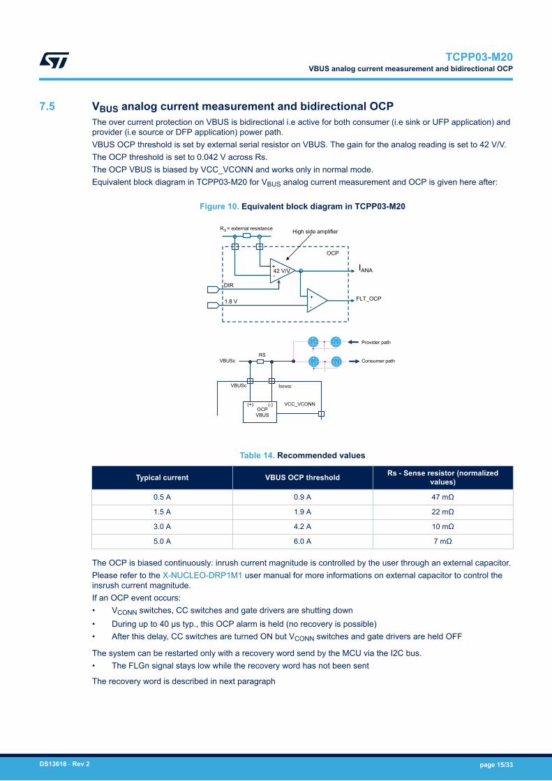
7.5 VBUS analog current measurement and bidirectional OCPThe over current protection on VBUS is bidirectional i.e active for both consumer (i.e sink or UFP application) andprovider (i.e source or DFP application) power path.VBUS OCP threshold is set by external serial resistor on VBUS. The gain for the analog reading is set to 42 V/V.The OCP threshold is set to 0.042 V across Rs.The OCP VBUS is biased by VCC_VCONN and works only in normal mode.Equivalent block diagram in TCPP03-M20 for VBUS analog current measurement and OCP is given here after:
Figure 10. Equivalent block diagram in TCPP03-M20
42 V/V
+
-
RS=external resistance
+-
OCP
Analog reading
High side amplifier
1.8 V
DIR
FLT_OCP
IANA
RS = external resistance
OCPVBUS
(+) (-)
Provider path
VBUSc
VBUSc ISENSE
RS
VCC_VCONN
Consumer path
Table 14. Recommended values
Typical current VBUS OCP threshold Rs - Sense resistor (normalizedvalues)
0.5 A 0.9 A 47 mΩ
1.5 A 1.9 A 22 mΩ
3.0 A 4.2 A 10 mΩ
5.0 A 6.0 A 7 mΩ
The OCP is biased continuously: inrush current magnitude is controlled by the user through an external capacitor.Please refer to the X-NUCLEO-DRP1M1 user manual for more informations on external capacitor to control theinsrush current magnitude.If an OCP event occurs:• VCONN switches, CC switches and gate drivers are shutting down• During up to 40 µs typ., this OCP alarm is held (no recovery is possible)• After this delay, CC switches are turned ON but VCONN switches and gate drivers are held OFF
The system can be restarted only with a recovery word send by the MCU via the I2C bus.• The FLGn signal stays low while the recovery word has not been sent
The recovery word is described in next paragraph
TCPP03-M20VBUS analog current measurement and bidirectional OCP
Figure 11. Typical chronograms of TCPP03-M20 VBUS OCP
ALARM HOLDINGOCP switch open
System OFF
NORMAL
SYSTEM ON
Gate driver ON OFF
TCPP ALARM HOLDINGSystem is waiting recovery word
up to 40 us
OCP switch closed
Over current
VBUS current
Note: • In case of VBUS OCP event, the TCPP03-M20 switches OFF all active functions except CC switches:– VCONN switches– VBUS gate driver (provider and consumer)– VCONN and VBUS discharge paths are activated
• It is signaled to the user by several ways:– I2C corresponding state bits are cleared (i.e. VCONN1_ACK = 0, VCONN2_ACK = 0…)– I2C relevant OCP flag is set (FLGn_OCP_VBUS is the OCP event coming from VBUS switch for
example)– Failure flag pin (FLGn) is active (i.e. in LowZ state)
• After a delay of up to 40 µs, to recover, the below bit sequence has to be written and after recovery, theuser can resume a start-up procedure:
Table 15. VBUS OCP recovery bit sequence table
Bit7 Bit6 Bit5 Bit4 Bit3 Bit2 Bit1 Bit0
0 0 PM2 PM1 1 0 0 0
TCPP03-M20VBUS analog current measurement and bidirectional OCP
DS13618 - Rev 2 page 16/33
7.6 VCONN OCP• At start-up, a soft start sets the tripping current to about 590 mA during 512 µs min. (1ms max.)• After this delay, the soft start is ended and the normal OCP threshold occurs (50 mA).• If an OCP event occurs:
– VCONN switches, CC switches and gate drivers are shutting down– During up to 40 µs typical, this OCP alarm is held (no recovery is possible)– After this delay, CC switches are turned ON but VCONN switches and gate drivers are held OFF. The
system can be restarted only with a recovery word send by the MCU via the I2C bus.– The FLGn signal stays low as long as the recovery word has not been sent
Figure 12. VCONN OCP chronograms
ALARM HOLDINGOCP switch open
System OFF
Soft start
SYSTEM ON
NORMAL
SYSTEM ON
Over currentVCONN current
Inrush current
512 µs (typ.)
VCONN switch ON OFF
StateALARM HOLDINGOCP switch open
System is waiting recovery word (CC switches ON)
up to 40 µs typ
OCP threshold is set to 590 mA OCP threshold is set to 47mA typ.
To recover, the below bit sequence has to be written and after recovery, the user can resume a start-upprocedure:
Table 16. VBUS OCP recovery bit sequence table
Bit7 Bit6 Bit5 Bit4 Bit3 Bit2 Bit1 Bit0
0 0 PM2 PM1 1 0 0 0
7.7 VCONN CC line OVP
7.7.1 CC lines short to VBUSThis happens when VBUS high voltage short circuit to the CC lines when hot unplug is done with a poormechanical quality connector. Over voltage protection is needed on the CC lines because VBUS typical voltagecan be as high as 20 V when CC pins are usually 5 V tolerant I/Os on low voltage USB-PHY controllers.TCPP03-M20 integrate this protection against CC lines short to VBUS thanks to an overvoltage protection(integrated FET).When the voltage on CC line goes above VTH_CC, the OVP on CC line turns-on in less than 60ns (TOVP_CCtypical value) and FLGn pin goes to '0' state.When the OVP event disappear, OVP on CC line is turned-off and the FLGn pin goes back to 'Hi-Z' state.
7.8 VBUS dischargeVBUS discharge is activated via I2C bus and controlled via firmware by the USB-C power delivery controller.The VBUS discharge feature integrated in TCPP02-M18 allows to discharge 10 µF in less than 220 ms(TDIS_VBUS).This discharge time is in line with USB-C specification, extracted below for VBUS discharge:
Table 17. Common source electrical parameters from USB-C specification
Parameter Description Min. Typ. Max. Units
tSafe0V Time to reachvSafe0V max. - - 650 ms
tSafe5V Time to reachvSafe5V max. - - 275 ms
7.9 VCONN dischargeVCONN discharge is activated via I2C bus and controlled via firmware by the USB-C power delivery controller.The VCONN discharge feature integrated in TCPP03-M20 allows to discharge VCONN in RDIS_VCONN < 5.5 kΩ, asper USB-C specification table extracted below:
Table 18. VCONN source characteristics from USB-C power delivery specification
Minimum Maximum Notes
Rdch 30 Ω 6120 Ω
Discharge resistance appliedin UnattachedWait.SRCbetween the CC pin beingdischarged and GND.
Note: • VCONN discharge is activated and stopped via I2C commands from USB-PD controller• To avoid short-circuit, VCONN discharge cannot be activated if VCONN switch are closed• The CCxc pin discharged is the last one acting as VCONN
7.10 OTP (over temperature protection)Above 150°C typ., the OTP triggers the FLGn pin.OVP and OCP on VCONN, CC lines, VBUS are shut down.Auto recovery is ensured when the temperature goes back below OTP threshold.
TCPP03-M20VBUS discharge
DS13618 - Rev 2 page 18/33
8 USB-C dual role power schematic example
Figure 13. Partial schematic extract of nucleo expansion board X-NUCLEO-DRP1M1 using TCPP03-M20
D-
D+
ZDiff90 ohms
ZDiff90 ohms
VBUS
3.3V
GNDGND
GND
GND
GND
GND
GND
GND
GND
GND
GND
GND
GND3.3V 3.3V
CC1CC2
I2C1_SDA
ENABLEI2C_ADD
DP
DP_other
DM
CC1_G4
Vsense
I2C1_SCL
SINK
SOURCE
ADC_Cons
ADC_Prov
ADC_VBUSc
ADC_Isense
FLGNR940.2k
R4140.2k
D9NMR40
200k
C9NM
C13
R4
2.2uF 50V
40.2kC12NM
CN1
CC1 A5
Dn1 A7
ConUSB31_632723300011_recep t
Dp1 A6
GN
D1GN
D1
GN
D2GN
D2
GND3 A1
GND5 A12
GND6B12
SBU1 A8
SHEL
L1SH
ELL1
SHEL
L2SH
ELL2
SHEL
L3SH
ELL3
SHEL
L4SH
ELL4
SHEL
L5SH
ELL5
SHEL
L6SH
ELL6
SSRXn1B10
SSRXn2 A10
SSRXp1B11
SSRXp2 A11
SSTXn1 A3SSTXp1 A2
VBUS1 A4
VBUS2 A9
VBUS4B9
Dn2B7
Dp2B6
GND4B1
SBU2B8
B3 SSTXn2B2 SSTXp2
VBUS3B4 CC2B5
C1
330pF 50V
CN21
1725656
2
R3200k
C2
R1
330pF 50V
10k
Q2B
D 5
G4
STL40DN3LLH5
3 S
C8NM
R29NM
CN312
1725656
Q1A
7 D
G2
STL40DN3LLH5
S 1
R121K
C3100n 50V 0
R30
Q2A
7 D
G2
STL40DN3LLH5
S 1
ESD ESD
ESD ESD
U3
2 D-
ECMF02-2AMX6
3 GND 4NC
D-1 5
D+1 61 D+
0R19
R8200k
SH11
R111K
R5
0.007
R1047K
U1
TCPP03-M20
20ENABLE
FLGn19
SCL18
SDA17
16I2C_ADD
CC1c15
CBIAS14
CC2c13
GND
12
11VSENSE
10ISENSE9VBUSc
8G
DCs
7G
DCg
6G
DPs
5G
DPg
4IANA
3CC2
2
CC11
VCC / VCONN
21ex
p pa
d G
ND
D10NM
TP3
Q1B
D 5
G4
STL40DN3LLH5
3 S
C10NM
C7
NM
TP1
SH13
TP2
TP4
TP5
D1
0R20
ESDA25P35-1U1M
C11
NM
CC1c
CC1cCC2c
CC2c
D+ D+ecmfD- D-ecmf
Isense
Vbus Max
22 V
17 V
13 V
10 V
6 V
P Max
100 W
45 W
36 W
27 W
15 W
GND
Vsense
R17 2.4k
R16 1.3k
R0 0
SH2
R15 976
R14 732
SH5
R2 560
SH4
SH3
Figure 14. STM32 configuration with CubeMX
TCPP03-M20USB-C dual role power schematic example
DS13618 - Rev 2 page 19/33
8.1 External components description
Table 19. Schematic description
Component reference Component name or value Description
D1 ESDA25P35-1U1M
TVS protecting against 25 A 8/20 µssurge waveforms and ESD transients(1)
(see Section 8.2 Transient Voltagesuppressor on VBUS).
C1, C2 330 pF typ., 25 V EMI capacitor, required to comply withUSB-C specification.
C3 100 nF, 50 VX7R ESD protection capacitance withlow ESL required to comply with USB-Cspecification.
C13 2,2 µF, 50 V VBUSc bulk capacitance, required in theUSB-C power delivery specification.
R5 0.007 Ω Serial resistor which value sets theVBUS OCP threshold.
R1 and R2 or R14, or R15, or R16, orR17 See Table 13 Resistor bridge to set VBUS OVP
threshold.
1. For more informations on USB type-C protection and filtering, cf AN4871, and AN3353 for informations related to IEC61000-4-2 standard testing.
8.2 Transient Voltage suppressor on VBUSThe D1 diode ESDA25P35-1U1M is used to comply with the international electrotechnical commissionspecification IEC61000-4-5 on the VBUS power line when it is subjected to switching and lightningtransients.These surges are defined in 8/20 µs waveform. For more information, please refer to AN4275:IEC61000-4-5 standard overview.
8.3 Configuration channel: line capacitance on CC1c and CC2cUSB-C PD has a specification for the total amount of capacitance for proper operation on CC lines. Thisspecification is given here after.
Table 20. USB-C PD specification
Description Minimum Maximum
CC receiver capacitance 200 pF 600 pF
Therefore, the capacitance added by the TCPP03-M20 and by the MCU or LV controller must fall within limits.The next table shows the analysis involved in choosing the correct external capacitor for the system.
Table 21. Table analysis
CC capacitance Min. Max. Comment
CC line target capacitor 200 pF 600 pF From USB PD Specificationsection 5.8.6
TCPP03-M20 capacitance 40 pF 100 pF
MCU or low voltagecapacitance 60 pF 90 pF
Typical value. To be adaptedfollowing the exact referenceused.
Proposed capacitance for C1,C2 120 pF 390 pF
25 VDC min. of rated voltage.
0402 or smallerrecommended.
C1 and C2 must be placed as close as possible to the USB-C connector to optimize the electromagneticimmunity.
8.4 Bulk capacitanceUSB-C power delivery specification defines cSnkBulk and cSrcBulk capacitances as the sum of bulk capacitanceson both sides of the ohmic path of VBUSc.To insure compliance with the standard and TCPP03-M20 protection performances, it is mandatory to place thiscapacitance on VBUSc, as close as possible to the USB-C connector with a value of 2,2 µF - 50 V.
TCPP03-M20Configuration channel: line capacitance on CC1c and CC2c
DS13618 - Rev 2 page 21/33
8.5 N-channel MOSFETThe TCPP03-M20 ensures a VGS voltage between 5 V and 6 V when the N-channel MOSFET is ON.The user must choose a N-channel MOSFET fully specified (for example: STL40DN3LLH5 in source to sourceconfiguration ) with 5 V of VGS. Maximum current in USB-PD applications can raises up to IDS = 5 A.As shown in Figure 15, C7 and C8 external capacitor may be associated to other N-channel MOSFET referenceto avoid OCP trigger due to inrush current on VBUS pin.
8.6 Complementary products for USB dataline ESD protection for pins DP, DM,SSRX, SSTXFor applications requiring USB dataline protection, STMicroelectronics recommends the implementation shown inpicture below:
Figure 16. USB dataline ESD protection for pins DP, DM, SSRX, SSTX
Table 22. Product recommendations
Part Number Description USB-Cconnector pin Protection features
TCPP03-M20 Type-C port protection VBUS, CC1, CC2,VCONN
ESD protection as per IEC61000-4-2 Level 4
Overvoltage, overcurrent and discharge onVBUS
Overvoltage, overcurrent and discharge onCC1/CC2, VCONN
ESDA25P35-1U1M Power line transient voltagesuppressor (TVS) VBUS
ESD protection as per IEC61000-4-2 Level 4
IEC61000-4-5 (8/20µs surge waveform)
ECMF02-2AMX6 Common mode filter withintegrated ESD protection D+, D-
ESD protection as per IEC61000-4-2 Level 4
RF antenna desense due to high speeddifferential link EMI radiation
ECMF4-2450A60N10(x2)
Common mode filter withintegrated ESD protection
TX1+, TX1-, RX1+,RX1-
TX2+, TX2-, RX2+,RX2-
ESD protection as per IEC61000-4-2 Level 4
RF antenna desense due to high speeddifferential link EMI radiation
For more information on USB Type-C protection for datalines, please refer to AN4871, USB Type-C protectionand filtering.For more information on RF antenna desense due to high speed differential link EMI radiation, please refer toAN4356, Antenna desense on handheld equipment.
TCPP03-M20Complementary products for USB dataline ESD protection for pins DP, DM, SSRX, SSTX
9.1 PCB routingWhen routing the TCPP03-M20, please respect the following recommendation:• Place the circuit as close as possible to the USB-C connector in order to maximize the efficiency of the ESD
protection for CC lines• Place the ESD capacitor as close as possible to the TCPP03-M20
TCPP03-M20PCB design recommendation
DS13618 - Rev 2 page 24/33
10 USB type-C port protection (TCPP) comparison table
Table 23. Device comparison table
Part number Expansion board SW expansion board USB type-C application Package
In order to meet environmental requirements, ST offers these devices in different grades of ECOPACK packages,depending on their level of environmental compliance. ECOPACK specifications, grade definitions and productstatus are available at: www.st.com. ECOPACK is an ST trademark.
TCPP03-M20QFN-20L 4.0 x 4.0 x 0.75 mm package information
DS13618 - Rev 2 page 30/33
12 Ordering information
Table 26. Ordering information
Order code Marking Package Weight Base qty. Delivery mode
TCPP03-M20 TCPP03 QFN-20L 4.0 x 4.0 x 0.75 mm 36.1 mg 3000 Tape and reel
TCPP03-M20Ordering information
DS13618 - Rev 2 page 31/33
Revision history
Table 27. Document revision history
Date Revision Changes
21-Jun-2021 1 Initial release.
04-Oct-2021 2 Updated Features, Table 6 and Table 26.
TCPP03-M20
DS13618 - Rev 2 page 32/33
IMPORTANT NOTICE – PLEASE READ CAREFULLY
STMicroelectronics NV and its subsidiaries (“ST”) reserve the right to make changes, corrections, enhancements, modifications, and improvements to STproducts and/or to this document at any time without notice. Purchasers should obtain the latest relevant information on ST products before placing orders. STproducts are sold pursuant to ST’s terms and conditions of sale in place at the time of order acknowledgement.
Purchasers are solely responsible for the choice, selection, and use of ST products and ST assumes no liability for application assistance or the design ofPurchasers’ products.
No license, express or implied, to any intellectual property right is granted by ST herein.
Resale of ST products with provisions different from the information set forth herein shall void any warranty granted by ST for such product.
ST and the ST logo are trademarks of ST. For additional information about ST trademarks, please refer to www.st.com/trademarks. All other product or servicenames are the property of their respective owners.
Information in this document supersedes and replaces information previously supplied in any prior versions of this document.


![M M20 SERIES Design Data Sheet - Isolator Design Data Sheet ... M20-530-08-[ ] M20-500-08-[ ] M20-470-08-[ ] ... 2.40 2160 559 1474 251 954 399 589 1753 497 1358 276 902 403 602 ISOLATOR](https://static.documents.pub/doc/80x56/5abf31ab7f8b9a8e3f8dfc28/m-m20-series-design-data-sheet-design-data-sheet-m20-530-08-m20-500-08-.jpg)


