I. Ferroelectric materials for piezoelectric, pyroelectric, and memory applications II. Nanoscale ferroelectrics ISIF-2005 Shanghai, April 17, 2005 Marin Alexe Max Planck Institute of Microstructure Physics Halle – Germany
Transcript
I. Ferroelectric materials for piezoelectric, pyroelectric, and memory applications II. Nanoscale ferroelectrics
ISIF-2005 Shanghai, April 17, 2005
Marin AlexeMax Planck Institute of Microstructure PhysicsHalle – Germany
Textbook– Ferroelectric crystals, F. Jona and G. Shirane, Pergamon, Oxford 1962– Principles and Applications of Ferroelectric Crystals …, M.E. Lines and A.M. Glass,
Clarendon, Oxford 1977– Ferroelectric memories, J. F. Scott, Berlin, Springer, 2000– Ferroelectric devices, K. Uchino, Dekker, 2000– Nanoelectronics and Information Technology, R. Waser (ed). Wiley-VCH, 2003
Edited books– Thin film ferroelectric materials and devices, R. Ramesh (ed.), Kluwer, 1997– Ferroelectric thin films : synthesis and basic properties, Paz de Araujo, Scott, and Taylor,
Gordon and Breach, 1996– Nanoscale phenomena in ferroelectric thin films, S. Hong (ed), Kluwer, 2004– Nanoscale characterisation of ferroelectric materials : scanning probe microscopy
approach, Alexe and Gruverman (eds), Springer, 2004Databases
– Landolt-Börnstein, vol. 16, Ferroelectric and related substances, ed. E. Nakamura, Springer, 1981
Review papers– The physics of ferroelectric ceramic thin films for memory applications, J.F. Scott,
Ferroelectrics Review 1, 1 (1998)– Ferroelectric, dielectric and piezoelectric properties of ferroelectric thin films and
ceramics, D. Damianovici, Rep. Prog. Phys. (61)1267 (1998)– Physics of this-film ferroelectric oxides, M. Dawber et al., Rev Mod. Phys., in press– M. Fiebig, Revival of the magnetoelectric effect, J. Phys. D, 38 (2005) R123 – etc.
Introduction
Mark Twain
"There are three kinds of lies: lies, damned lies and statistics.“
Introduction
02000400060008000
10000120001400016000
1970-1975
1981-1985
1991-1995
2001-2005
Papers onFerroelectrics
INSPEC database
020000400006000080000
100000120000140000160000
1970-1975
1981-1985
1991-1995
2001-2005
Papers onSemiconductors
0
0,02
0,04
0,06
0,08
0,1
0,12
1970-1975
1981-1985
1991-1995
2001-2005
Ferro/Semicon
02468
101214161820
1970-1975
1981-1985
1991-1995
2001-2005
Nature & Science
Ferroelectrics
Basics of ferroelectricity
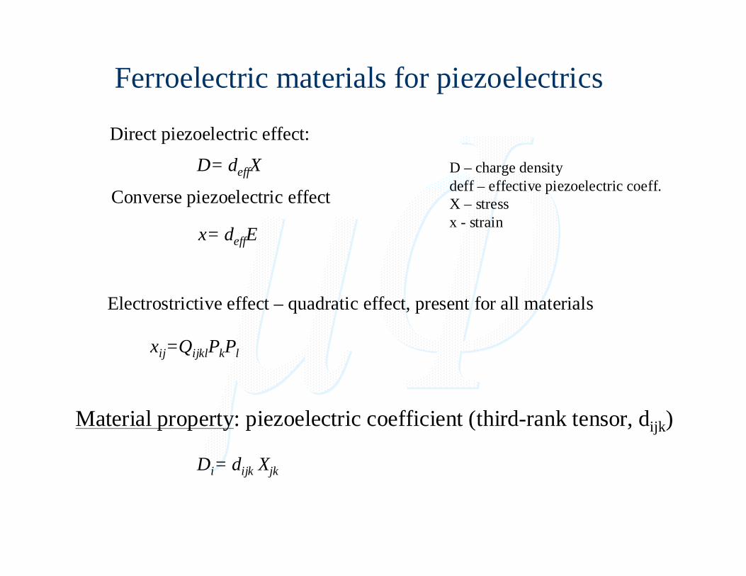
Piezolectrics:– Charge generation by mechanical fields
Pyroelectrics:– Charge generation by thermal fields
Ferroelectrics:– Charge generation by electrical fields
What are they good for?
And converse !
Basics of …
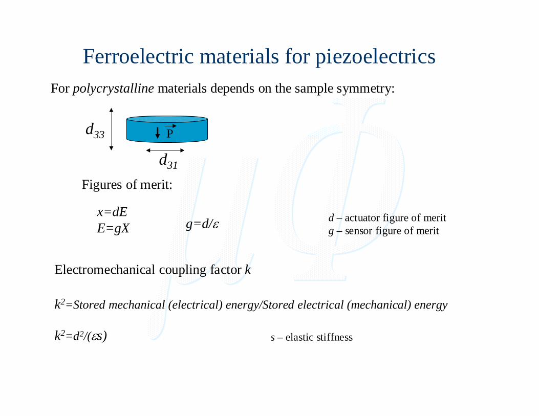
What are they good for?Piezoelectrics– Mechanical strain (stress) ⇔ Electric field (charge)
E
Basics of …
What are they good for?Piezoelectrics– Mechanical strain (stress) ⇔ Electric field (charge)
Stress X
+Q
-Q
P
D= deffX
Di= dijkXjk
D – charge densitydeff – effective piezoelectric coeff.X – stress
Basics of …
What are they good for?Pyroelectrics– Thermal variation ⇔ Charge generation
∆T
+Q
-Q
P
∆Q=p∆T
Ferroelectrics– Switching by electrical field ⇔ Charge generation
Basics of …
P
E -6 -4 -2 0 2 4 6
-60
-40
-20
0
20
40
60 P
V
P-E Characteristics (hysteresis loop)
What are they good for?
∆Q=2Pr
Applications
The physics of ferroelectric memories, Auciello O, Scott JF, Ramesh R., Physics Today 51, p22, July 1998
Ferroelectricity – symmetry-based phenomenon
Electrostrictive32 classes
No symmetry centre21 classes
Piezoelectric20 classes
Non-piezoelectric1 class
Pyroelectric10 classes
Non-Pyroelectric10 class
symmetry centre11 classes
Ferroelectric
Ion shift in the perovkite cell
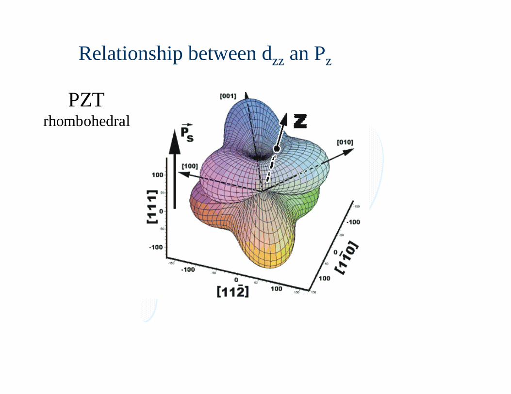
Ferroelectric Materials
Main ferroelectric oxides
Pb-based materials - Pb(Zr,Ti)O3
Layered perovkites – SrBi2Ta2O9, Bi4Ti3O12
BaTiO3-based materials – (Ba,Sr)TiO3
There are >500 ferroelectric compounds (without solid-solutions)– Landolt-Bornstein, Ferro- and Antiferroelectric Substances, Springer, 1975
For most demanding applications only oxides are seriously consideredChoosing the optimum material is an application-dependent problem
Ferroelectric Materials
Ferroelectric materials for piezoelectric applications
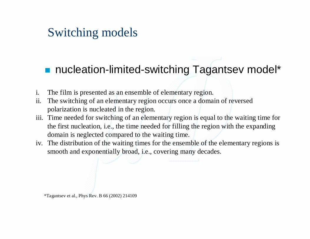
i. The film is presented as an ensemble of elementary region.ii. The switching of an elementary region occurs once a domain of reversed
polarization is nucleated in the region.iii. Time needed for switching of an elementary region is equal to the waiting time for
the first nucleation, i.e., the time needed for filling the region with the expanding domain is neglected compared to the waiting time.
iv. The distribution of the waiting times for the ensemble of the elementary regions is smooth and exponentially broad, i.e., covering many decades.
Switching models
Du-Chen model*
*X. Du and I. W. Chen, MRS Proc. 493 (1998) 311D.J. Jung et al., Integrated Feroelectrics 48 (2002) 59
-nucleation process is connected to defects (pinning) -nucleation is thermally activated
2011lnln
CEG
kTff ∆−=
Ec – coecive fieldf – frequency∆G – critical energy
to form a nuclei
⎟⎟⎠
⎞⎜⎜⎝
⎛∆= 20
11expCE
GkT
ττ
Ferroelectric Materials
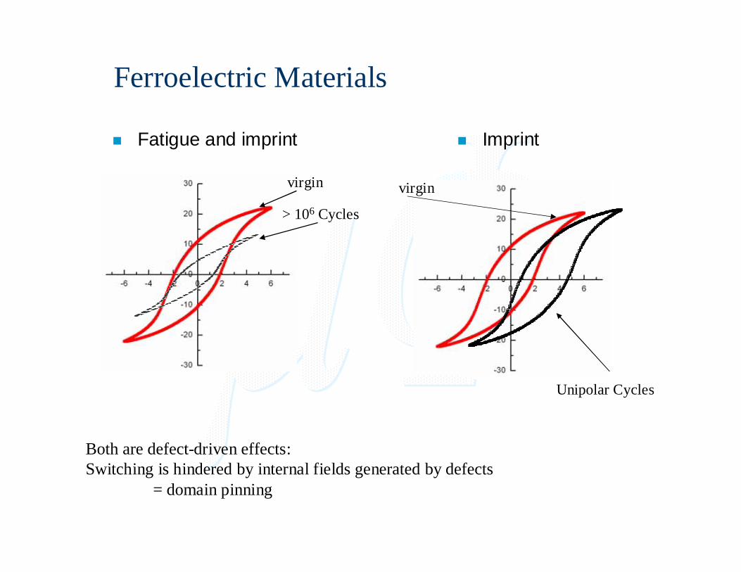
Fatigue and imprint
Both are defect-driven effects:Switching is hindered by internal fields generated by defects
= domain pinning
virgin
> 106 Cycles
Imprint
virgin
Unipolar Cycles
Ferroelectric Materials
Simple perovskites – ABO3
– Pb(Zr,Ti)O3 – PZT – BaTiO3
Layered perovskites
– SrBi2Ta2O9 – SBT – Bi4Ti3O12 – BiT
A
B
O
TiO6
O
Ti
Bi
TaO6
O
Ta
Bi
Sr
Multiferroics
Multiferroics
Elastic Magnetic
Electric
Ferro ≡ two or more states exists and can be shifted by field
ParaFerroAntiferro
Magneto-elastic
Ferro-elastic Magneto-electric
Multiferroics
Lines and Glass, Principles and applications of ferroelectrics…, Clarendon Press, Oxford, 1977
Multiferroics
Lines and Glass, Principles and applications of ferroelectrics…, Clarendon Press, Oxford, 1977
2. Coupled elastic and magnetic properties – Magnetoelastic:
K2NiF4 : PPP → PFcAc
3. Coupled electric and magnetic properties – Magnetoelectric:
1. Coupled elastic and electric properties – Ferroelastic:
BaTiO3: PPP→FcFcP →FcFcP →FcFcP
RbFeF4 : PPP → PFP → PFA
BaCoF4 : PPP → FPP → FFA
Examples
Multiferroics
*Wang et al., Epitaxial BiFeO3 multiferroic thin film heterostructures, Science (2003) 1719** Erenstein et al Comment on “Epitaxial BiFeO3 Multiferroic Thin Film Heterostructures”, Nature
Example 1 – Ferroelectric and Ferromagnetic*: BiFeO3 – thin epitaxial films
dE/dHMagnetoelectric coefficient
Multiferroics
*Zheng et al., Multiferroic BaTiO3-CoFe2O4 Nanostructures, Science (2004) 661
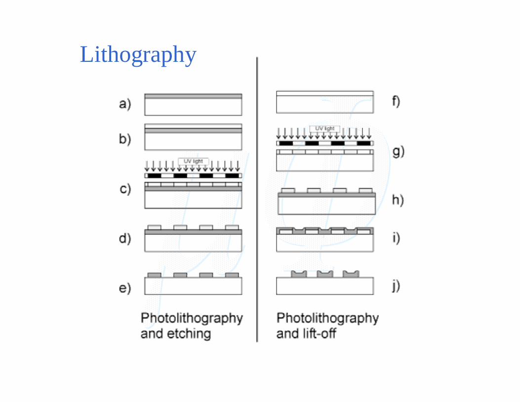
Nanosize ferroelectrics fabricated by self-assembly methods
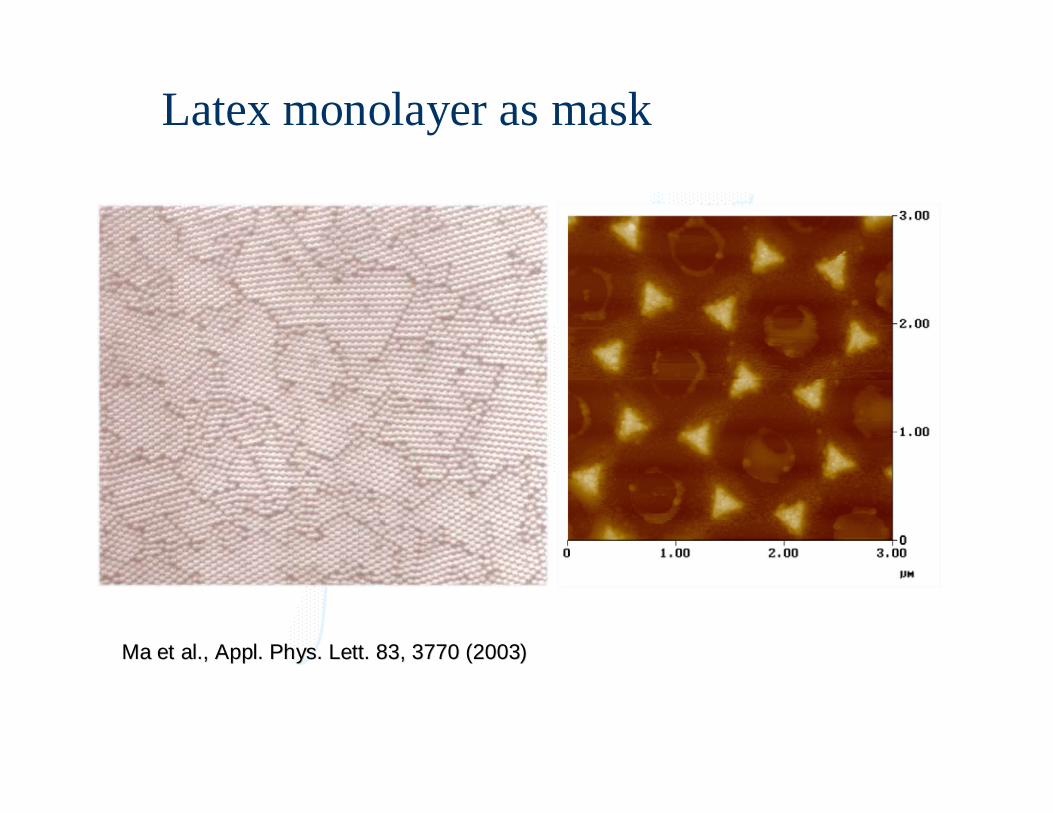
Latex monolayer as mask
Ma et al., Appl. Phys. Lett. 83, 3770 (2003)Ma et al., Appl. Phys. Lett. 83, 3770 (2003)
Self-assembly methods
Island growth mode of MOCVDIsland growth mode of MOCVDM. Shimizu et al.M. Shimizu et al.
Tune the growth conditions to Tune the growth conditions to achieve island growth mode, achieve island growth mode, which allows fabrication of which allows fabrication of nanoscale islands nanoscale islands
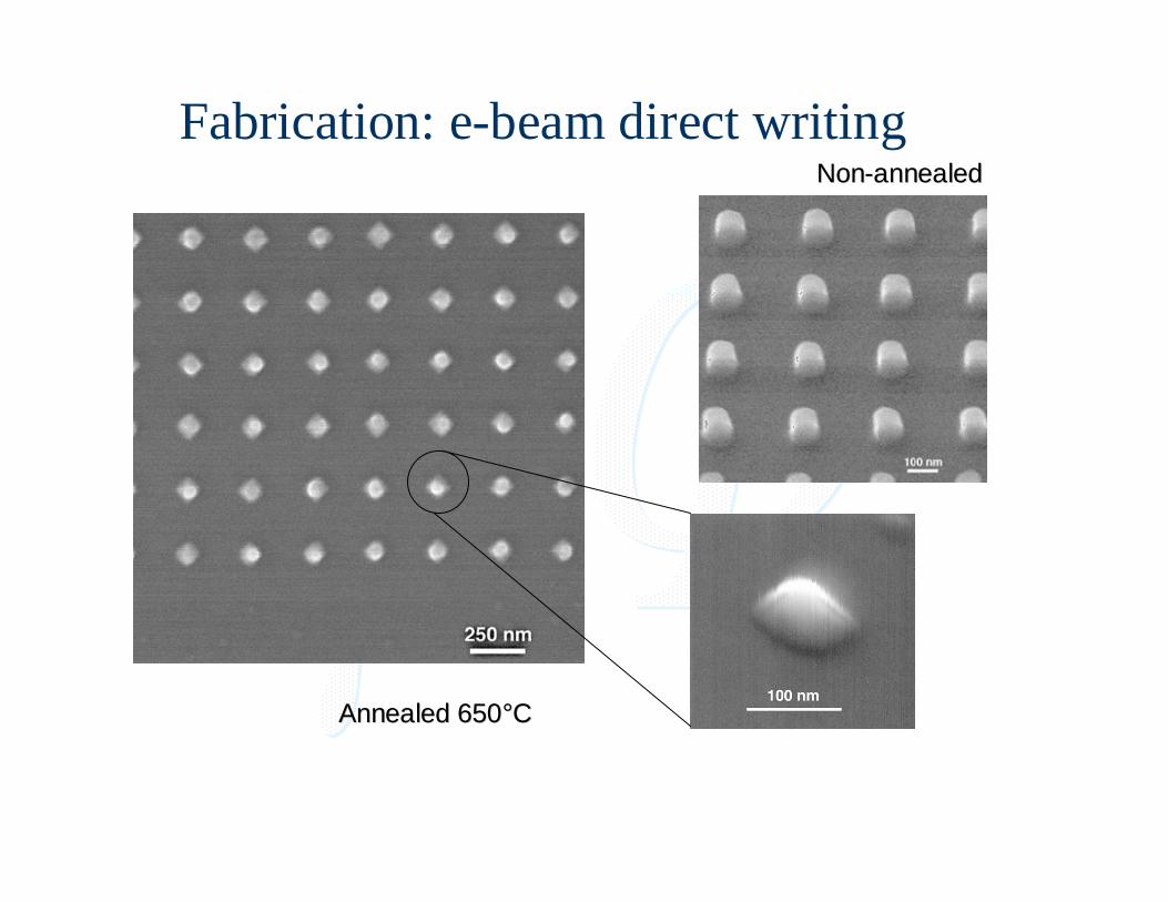
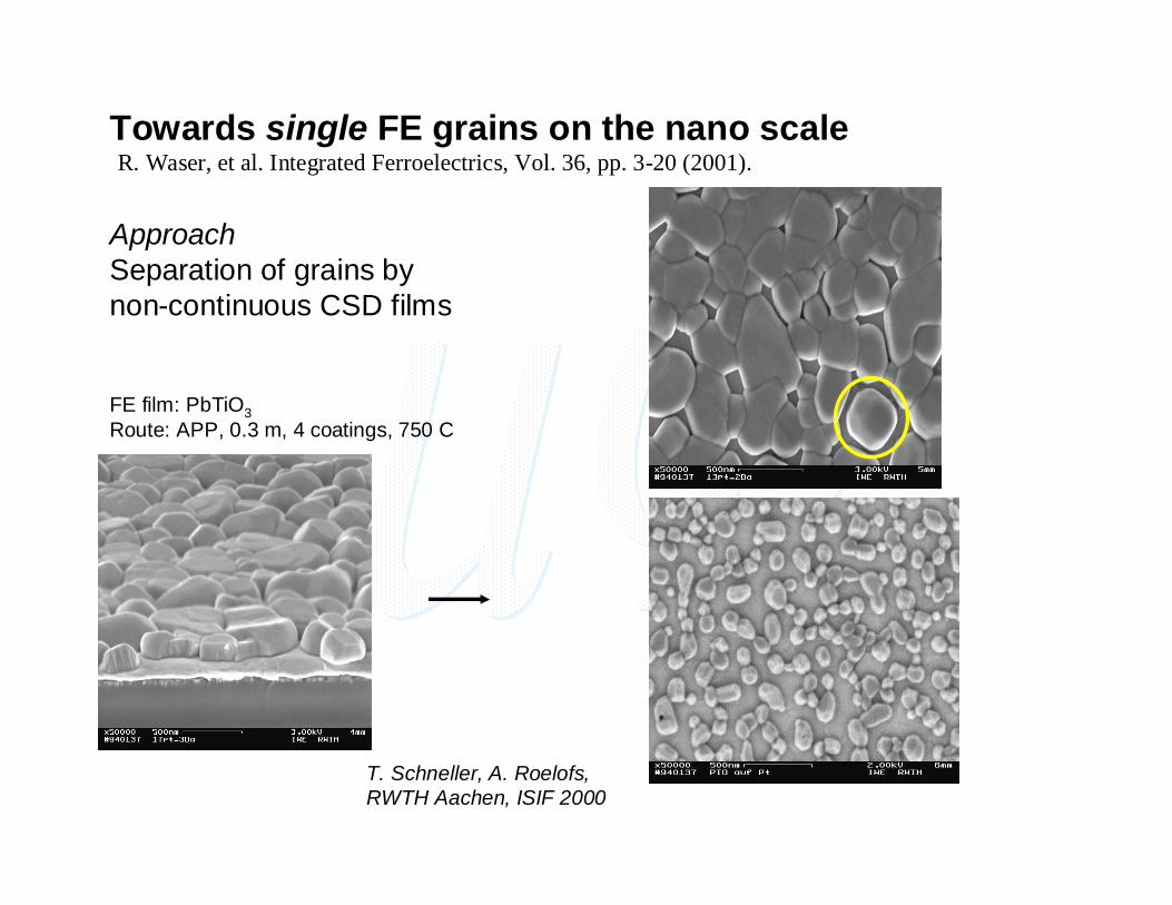
Towards single FE grains on the nano scale
T. Schneller, A. Roelofs, RWTH Aachen, ISIF 2000
ApproachSeparation of grains bynon-continuous CSD films
FE film: PbTiO3Route: APP, 0.3 m, 4 coatings, 750 C
R. Waser, et al. Integrated Ferroelectrics, Vol. 36, pp. 3-20 (2001).
A. Seifert, A. Vojta, J.S. Speck, F.F. Lange, J. Mater. Res. 11 (1996) 1470.
Ferroelectric nano-crystals by self-assembly
Microstructural instability in epitaxial ultraMicrostructural instability in epitaxial ultra--thin CSDthin CSD--deposited films deposited films
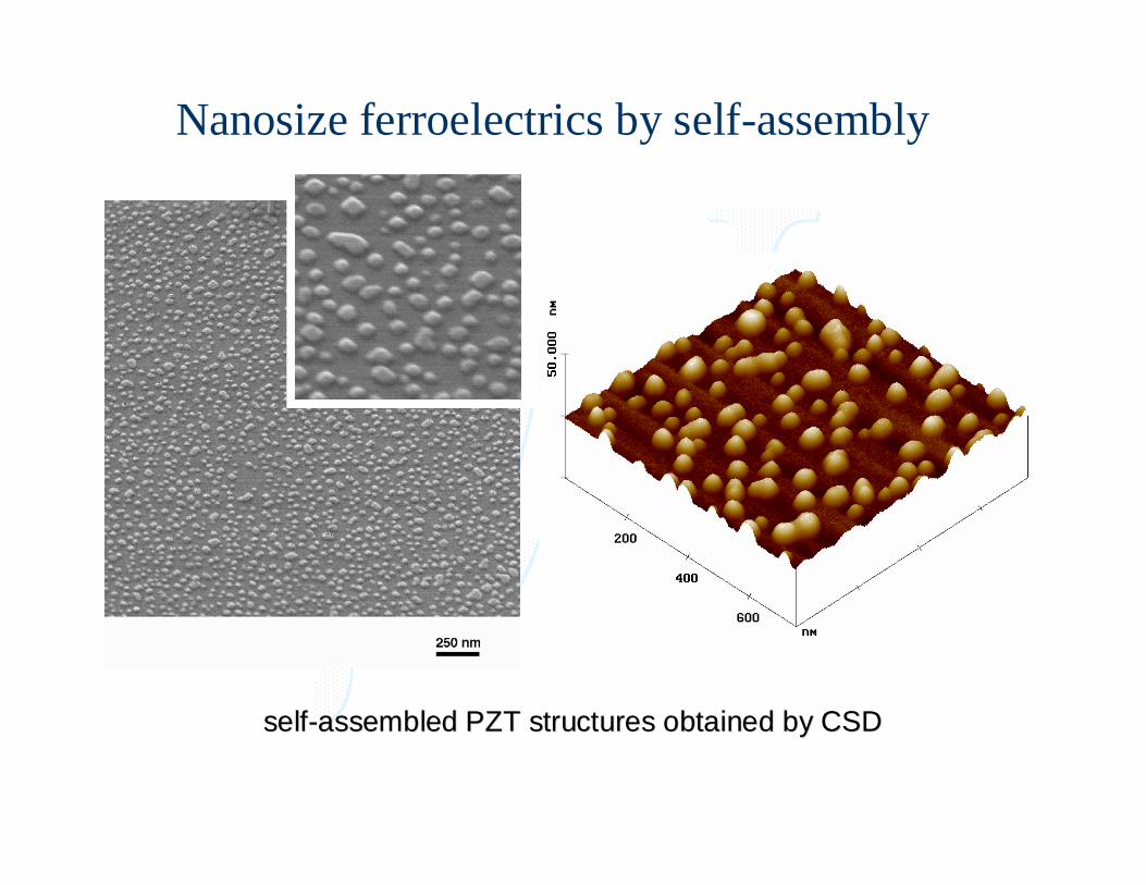
Nanosize ferroelectrics by self-assembly
selfself--assembled PZT structures obtained by CSDassembled PZT structures obtained by CSD
X-ray diffraction pattern
10 20 30 40 50 60 70 80
In
tens
ity (a
. u.)
2θ (deg.)
100
STO
300
STO20
0S
TO
300
PZT
200
PZT
100
PZT
200
STO
, Kβ
300
STO
, Kβ
Structural investigations - XRD
Annealing temperature
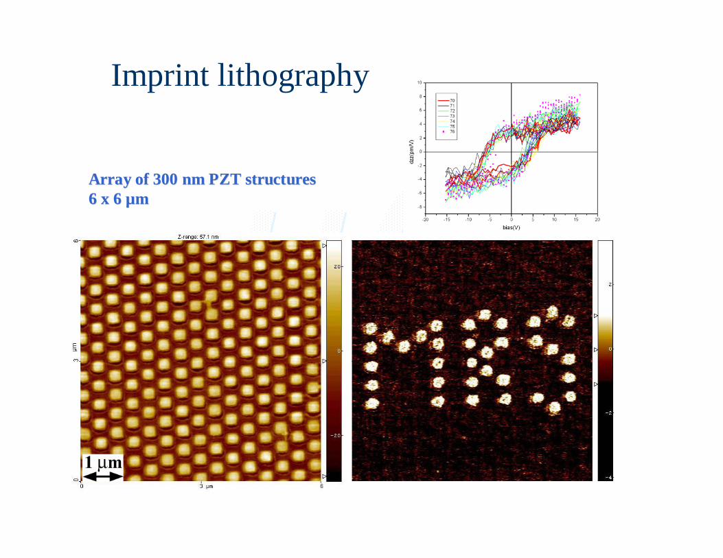
Nanosize ferroelectrics by self-patterning
800oC 950oC 1100oC
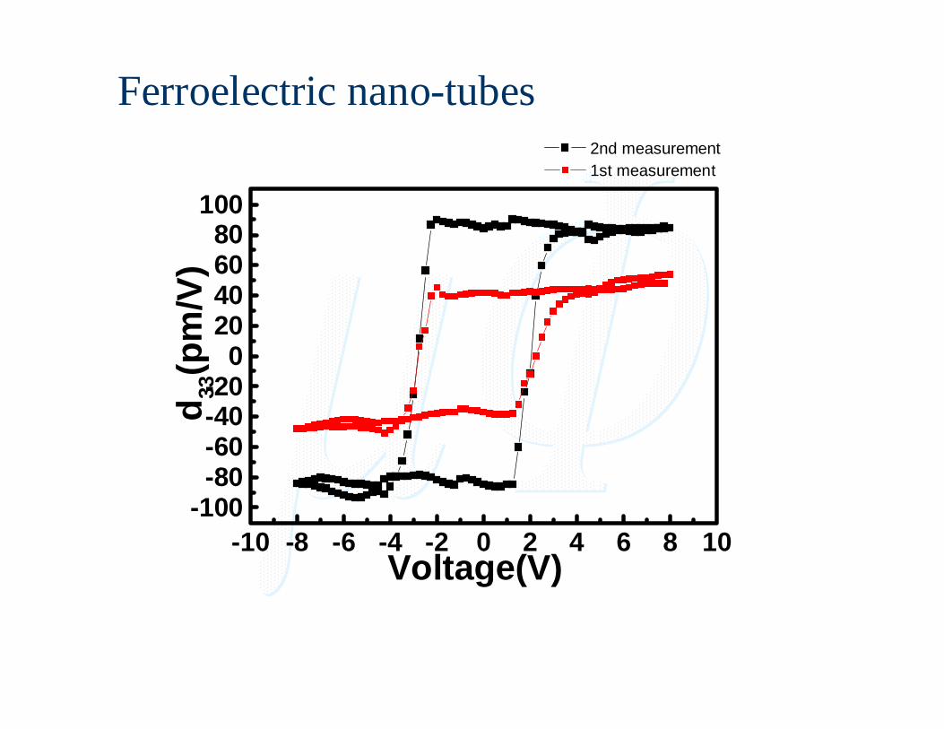
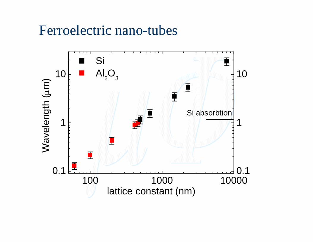
1- D ferroelectric systems
Nanowires
Ferroelectric nanowires
H. Park, Harvard UniversityNanoletters 2, 447 (2002)
Ferroelectric nanowires
H. Park, Harvard UniversityH. Park, Harvard UniversityNanolettersNanoletters 2, 447 (2002)2, 447 (2002)


![Fabrication and Characterization of PZN-4.5PT Inorganic ...[26], showing at least ferroelectric, ferroelastic and piezoelectric properties. However, the greatest difficulty to use](https://static.documents.pub/doc/80x56/6109a06ad373db57b45234c7/fabrication-and-characterization-of-pzn-45pt-inorganic-26-showing-at-least.jpg)