Atmel-8719B-SEEPROM-AT24C16C-Datasheet_042013 Standard Features Low-voltage and standard-voltage operation V CC = 1.7V to 5.5V Internally organized as 2,048 x 8 (16K) I 2 C-compatible (2-wire) serial interface Schmitt Trigger, filtered inputs for noise suppression Bidirectional data transfer protocol 1MHz (2.5V, 2.7V, 5V), 400kHz (1.7V) compatibility Write Protect pin for hardware data protection 16-byte Page Write mode Partial page writes allowed Self-timed write cycle (5ms max) High-reliability Endurance: 1,000,000 write cycles Data retention: 100 years Green package options (Pb/Halide-free/RoHS compliant) 8-lead PDIP, 8-lead SOIC, 8-lead TSSOP, 8-pad UDFN, 8-pad XDFN, 5-lead SOT23, and 8-ball VFBGA Die options: wafer form and tape and reel Description The Atmel ® AT24C16C provides 16,384 bits of Serial Electrically Erasable and Programmable Read-Only Memory (EEPROM) organized as 2,048 words of eight bits each. The device is optimized for use in many industrial and commercial applications where low-power and low-voltage operation are essential. AT24C16C is available in space-saving 8-lead PDIP, 8-lead JEDEC SOIC, 8-lead TSSOP, 8-pad UDFN, 8-pad XDFN, 5-lead SOT23, and 8-ball VFBGA packages and is accessed via a 2-wire serial interface. Atmel AT24C16C I 2 C-Compatible, (2-Wire) Serial EEPROM 16-Kbit (2048 x 8) DATASHEET
Transcript
Atmel AT24C16C
I2C-Compatible, (2-Wire) Serial EEPROM16-Kbit (2048 x 8)
DATASHEET
Standard Features
Low-voltage and standard-voltage operation VCC = 1.7V to 5.5V
Internally organized as 2,048 x 8 (16K) I2C-compatible (2-wire) serial interface Schmitt Trigger, filtered inputs for noise suppression Bidirectional data transfer protocol 1MHz (2.5V, 2.7V, 5V), 400kHz (1.7V) compatibility Write Protect pin for hardware data protection 16-byte Page Write mode
5-lead SOT23, and 8-ball VFBGA Die options: wafer form and tape and reel
Description
The Atmel® AT24C16C provides 16,384 bits of Serial Electrically Erasable and Programmable Read-Only Memory (EEPROM) organized as 2,048 words of eight bits each. The device is optimized for use in many industrial and commercial applications where low-power and low-voltage operation are essential. AT24C16C is available in space-saving 8-lead PDIP, 8-lead JEDEC SOIC, 8-lead TSSOP, 8-pad UDFN, 8-pad XDFN, 5-lead SOT23, and 8-ball VFBGA packages and is accessed via a 2-wire serial interface.
Atmel-8719B-SEEPROM-AT24C16C-Datasheet_042013
1. Pin Configurations and Pinouts
Table 1. Pin Configuration
2. Absolute Maximum Ratings
Pin Name Function
NC No Connect
SDA Serial Data
SCL Serial Clock Input
WP Write Protect
GND Ground
VCC Power Supply
1
2
3
4
8
7
6
5
NC
NC
NC
GND
VCC
WP
SCL
SDA
8-lead PDIP
1
2
3
5
4
SCL
GND
SDA
WP
VCC
5-lead SOT23
VCC
WP
SCL
SDA
NC
NC
NC
GND
1
2
3
4
8
7
6
5
8-ball VFBGA
Bottom View
Note: Drawings are not to scale.
8-pad UDFN/XDFN
Bottom View
Top ViewTop View
Top View
Top View
VCC
WP
SCL
SDA
NC
NC
NC
GND
1
2
3
4
8
7
6
5
8-lead TSSOP
1234
8765
NCNCNC
GND
VCCWPSCLSDA
8-lead SOIC
NC
NC
NC
GND
VCC
WP
SCL
SDA
1
2
3
4
8
7
6
5
Operating Temperature . . . . . . . . . . .–55C to +125C
Storage Temperature . . . . . . . . . . . .–65C to +150C
Voltage on any pinwith respect to ground . . . . . . . . . . . . . –1.0V to +7.0V
Maximum Operating Voltage . . . . . . . . . . . . . . . 6.25V
*Notice: Stresses beyond those listed under “Absolute Maximum Ratings” may cause permanent damage to the device. This is a stress rating only and functional operation of the device at these or any other conditions beyond those indicated in the operational sections of this specification is not implied. Exposure to absolute maximum rating conditions for extended periods may affect device reliability.
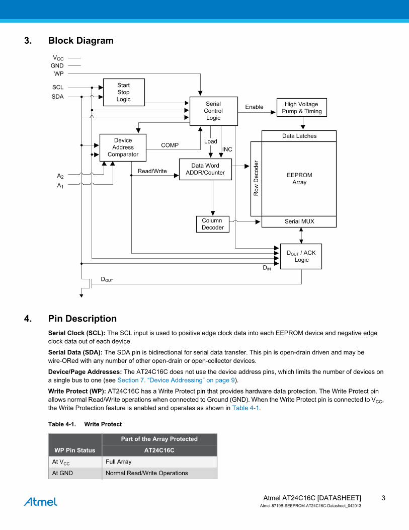
4. Pin DescriptionSerial Clock (SCL): The SCL input is used to positive edge clock data into each EEPROM device and negative edge clock data out of each device.
Serial Data (SDA): The SDA pin is bidirectional for serial data transfer. This pin is open-drain driven and may be wire-ORed with any number of other open-drain or open-collector devices.
Device/Page Addresses: The AT24C16C does not use the device address pins, which limits the number of devices on a single bus to one (see Section 7. “Device Addressing” on page 9).
Write Protect (WP): AT24C16C has a Write Protect pin that provides hardware data protection. The Write Protect pin allows normal Read/Write operations when connected to Ground (GND). When the Write Protect pin is connected to VCC, the Write Protection feature is enabled and operates as shown in Table 4-1.
5. Memory OrganizationAT24C16C, 16K Serial EEPROM: Internally organized with 128 pages of 16 bytes each, the 16K requires a 11-bit data word address for random word addressing.
Table 5-1. Pin Capacitance(1)
Note: 1. This parameter is characterized and is not 100% tested.
Table 5-2. DC Characteristics
Note: 1. VIL min and VIH max are reference only and are not tested.
Applicable over recommended operating range from TA = 25°C, f = 1.0MHz, VCC = 5.5V.
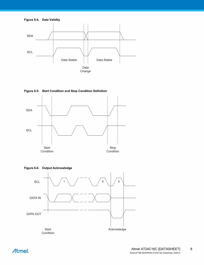
6. Device Operation Clock and Data Transitions: The SDA pin is normally pulled high with an external device. Data on the SDA pin may change only during SCL low time periods (see Figure 6-4 on page 8). Data changes during SCL high periods will indicate a Start or Stop Condition as defined below.
Start Condition: A high-to-low transition of SDA with SCL high is a Start Condition which must precede any other command (see Figure 6-5 on page 8).
Stop Condition: A low-to-high transition of SDA with SCL high is a Stop Condition. After a read sequence, the Stop Condition command will place the EEPROM in a standby power mode (see Figure 6-5 on page 8).
Acknowledge: All addresses and data words are serially transmitted to and from the EEPROM in eight bit words. The EEPROM sends a zero to acknowledge that it has received each word. This happens during the ninth clock cycle.
Standby Mode: The AT24C16C features a low-power standby mode which is enabled: Upon power-up. After the receipt of the Stop Condition and the completion of any internal operations.
2-wire Software Reset: After an interruption in protocol, power loss or system reset, any 2-wire part can be reset by following these steps:
1. Create a Start Condition,2. Clock nine cycles,3. Create another Start Condition followed by Stop Condition as shown below.
The device is ready for next communication after above steps have been completed.
7. Device AddressingStandard EEPROM Access: The 16K EEPROM device requires an 8-bit device address word following a Start Condition to enable the chip for a Read or Write operation. The device address word consists of a mandatory “1010” (Ah) sequence for the first four Most Significant Bits (MSB) as shown in Figure 10. on page 12. This is common to all the EEPROM devices.
The next three bits used for memory page addressing are the most significant bits of the data word address which follows.
The eighth bit of the device address is the Read/Write operation select bit. A Read operation is initiated if this bit is high and a Write operation is initiated if this bit is low.
Upon a compare of the device address, the EEPROM will output a zero. If a compare is not made, the chip will return to a standby state.
Figure 7-1. Device Address
8. Write OperationsByte Write: A Write operation requires an 8-bit data word address following the device address word and acknowledgment. Upon receipt of this address, the EEPROM will again respond with a zero and then clock in the first 8-bit data word. Following receipt of the 8-bit data word, the EEPROM will output a zero and the addressing device, such as a microcontroller, must terminate the Write sequence with a Stop Condition. At this time the EEPROM enters an internally timed write cycle, tWR, to the nonvolatile memory. All inputs are disabled during this write cycle and the EEPROM will not respond until the Write is complete (see Figure 8-1).
Figure 8-1. Byte Write
Density Access Area Bit 7 Bit 6 Bit 5 Bit 4 Bit 3 Bit 2 Bit 1 Bit 0
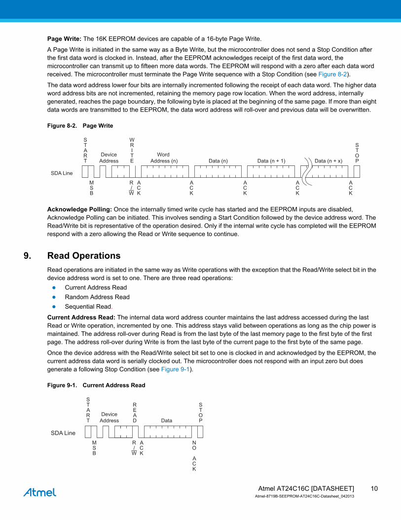
Page Write: The 16K EEPROM devices are capable of a 16-byte Page Write.
A Page Write is initiated in the same way as a Byte Write, but the microcontroller does not send a Stop Condition after the first data word is clocked in. Instead, after the EEPROM acknowledges receipt of the first data word, the microcontroller can transmit up to fifteen more data words. The EEPROM will respond with a zero after each data word received. The microcontroller must terminate the Page Write sequence with a Stop Condition (see Figure 8-2).
The data word address lower four bits are internally incremented following the receipt of each data word. The higher data word address bits are not incremented, retaining the memory page row location. When the word address, internally generated, reaches the page boundary, the following byte is placed at the beginning of the same page. If more than eight data words are transmitted to the EEPROM, the data word address will roll-over and previous data will be overwritten.
Figure 8-2. Page Write
Acknowledge Polling: Once the internally timed write cycle has started and the EEPROM inputs are disabled, Acknowledge Polling can be initiated. This involves sending a Start Condition followed by the device address word. The Read/Write bit is representative of the operation desired. Only if the internal write cycle has completed will the EEPROM respond with a zero allowing the Read or Write sequence to continue.
9. Read OperationsRead operations are initiated in the same way as Write operations with the exception that the Read/Write select bit in the device address word is set to one. There are three read operations: Current Address Read Random Address Read Sequential Read.
Current Address Read: The internal data word address counter maintains the last address accessed during the last Read or Write operation, incremented by one. This address stays valid between operations as long as the chip power is maintained. The address roll-over during Read is from the last byte of the last memory page to the first byte of the first page. The address roll-over during Write is from the last byte of the current page to the first byte of the same page.
Once the device address with the Read/Write select bit set to one is clocked in and acknowledged by the EEPROM, the current address data word is serially clocked out. The microcontroller does not respond with an input zero but does generate a following Stop Condition (see Figure 9-1).
Figure 9-1. Current Address Read
SDA Line
START
WRITE
STOP
DeviceAddress
Word Address (n) Data (n) Data (n + 1) Data (n + x)
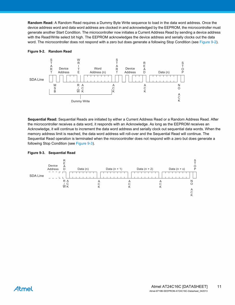
Random Read: A Random Read requires a Dummy Byte Write sequence to load in the data word address. Once the device address word and data word address are clocked in and acknowledged by the EEPROM, the microcontroller must generate another Start Condition. The microcontroller now initiates a Current Address Read by sending a device address with the Read/Write select bit high. The EEPROM acknowledges the device address and serially clocks out the data word. The microcontroller does not respond with a zero but does generate a following Stop Condition (see Figure 9-2).
Figure 9-2. Random Read
Sequential Read: Sequential Reads are initiated by either a Current Address Read or a Random Address Read. After the microcontroller receives a data word, it responds with an Acknowledge. As long as the EEPROM receives an Acknowledge, it will continue to increment the data word address and serially clock out sequential data words. When the memory address limit is reached, the data word address will roll-over and the Sequential Read will continue. The Sequential Read operation is terminated when the microcontroller does not respond with a zero but does generate a following Stop Condition (see Figure 9-3).
Figure 9-3. Sequential Read
SDA Line
START
START
READ
WRITE
STOP
DeviceAddress
DeviceAddress
WordAddress (n) Data (n)
MSB
ACK
ACK
ACK
NO
ACK
R/
W
Dummy Write
SDA Line
READ
STOP
DeviceAddress Data (n) Data (n + 1) Data (n + 2) Data (n + x)
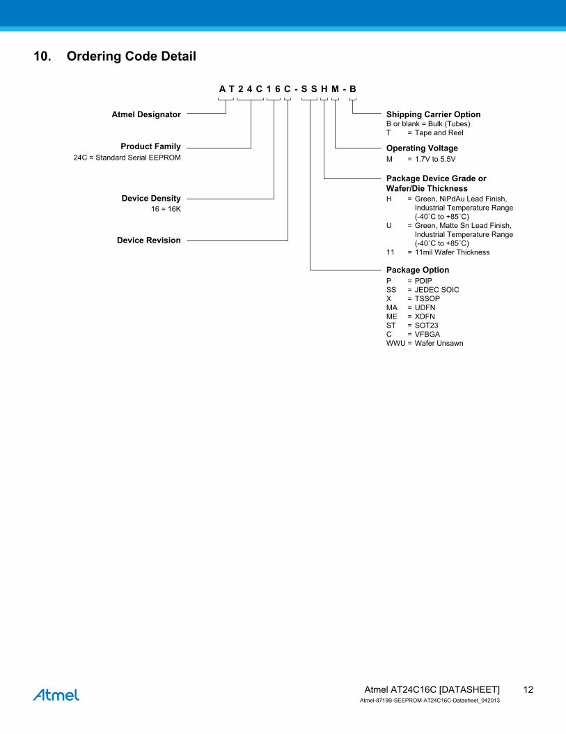
Package Device Grade or Wafer/Die ThicknessH = Green, NiPdAu Lead Finish, Industrial Temperature Range (-40˚C to +85˚C)U = Green, Matte Sn Lead Finish, Industrial Temperature Range (-40˚C to +85˚C)11 = 11mil Wafer Thickness
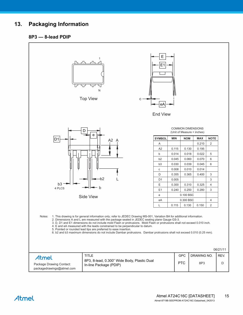
Notes: 1. This drawing is for general information only; refer to JEDEC Drawing MS-001, Variation BA for additional information. 2. Dimensions A and L are measured with the package seated in JEDEC seating plane Gauge GS-3. 3. D, D1 and E1 dimensions do not include mold Flash or protrusions. Mold Flash or protrusions shall not exceed 0.010 inch. 4. E and eA measured with the leads constrained to be perpendicular to datum. 5. Pointed or rounded lead tips are preferred to ease insertion. 6. b2 and b3 maximum dimensions do not include Dambar protrusions. Dambar protrusions shall not exceed 0.010 (0.25 mm).
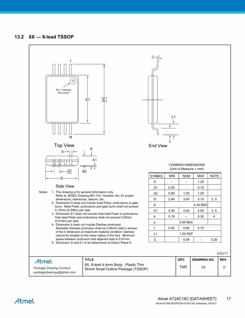
Notes: 1. This drawing is for general information only. Refer to JEDEC Drawing MO-153, Variation AA, for proper dimensions, tolerances, datums, etc. 2. Dimension D does not include mold Flash, protrusions or gate burrs. Mold Flash, protrusions and gate burrs shall not exceed 0.15mm (0.006in) per side. 3. Dimension E1 does not include inter-lead Flash or protrusions. Inter-lead Flash and protrusions shall not exceed 0.25mm (0.010in) per side. 4. Dimension b does not include Dambar protrusion. Allowable Dambar protrusion shall be 0.08mm total in excess of the b dimension at maximum material condition. Dambar cannot be located on the lower radius of the foot. Minimum space between protrusion and adjacent lead is 0.07mm. 5. Dimension D and E1 to be determined at Datum Plane H.
A - - 1.00 A1 0.00 - 0.10 A2 0.70 0.90 1.00 c 0.08 - 0.20 3 D 2.90 BSC 1,2 E 2.80 BSC 1,2 E1 1.60 BSC 1,2 L1 0.60 REF e 0.95 BSC e1 1.90 BSC b 0.30 - 0.50 3,4
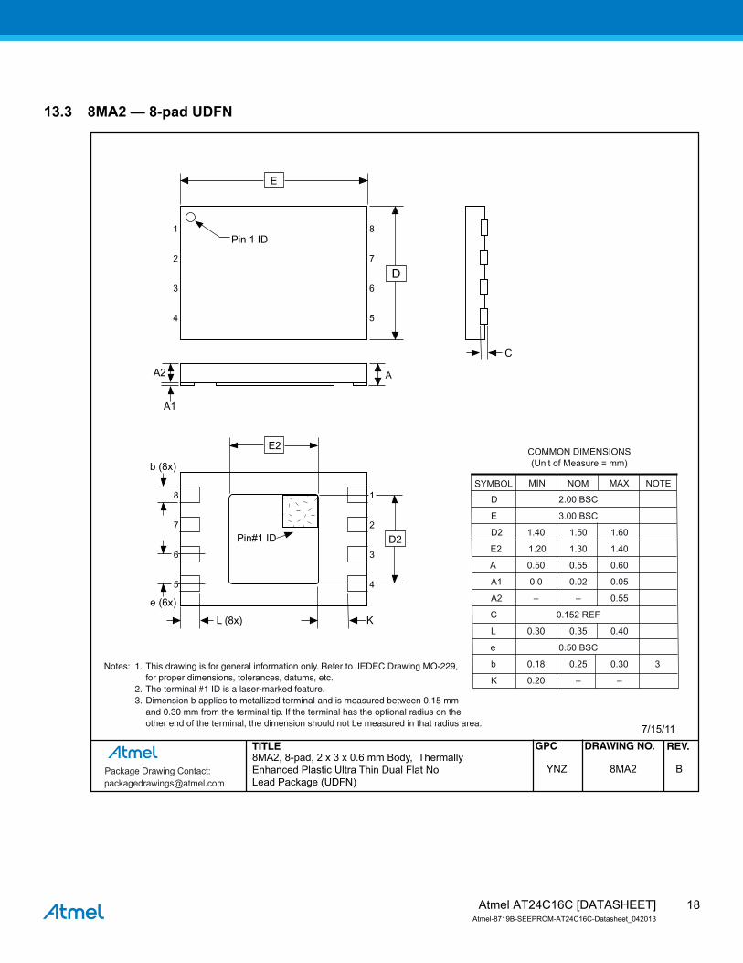
1. Dimension D does not include mold flash, protrusions or gate burrs. Mold flash, protrusions or gate burrs shall not exceed 0.15 mm per end. Dimension E1 does not include interlead flash or protrusion. Interlead flash or protrusion shall not exceed 0.15 mm per side. 2. The package top may be smaller than the package bottom. Dimensions D and E1 are determined at the outermost extremes of the plastic body exclusive of mold flash, tie bar burrs, gate burrs and interlead flash, but including any mismatch between the top and bottom of the plastic body.3. These dimensions apply to the flat section of the lead between 0.08 mm and 0.15 mm from the lead tip.4. Dimension "b" does not include dambar protrusion. Allowable dambar protrusion shall be 0.08 mm total in excess of the "b" dimension at maximum material condition. The dambar cannot be located on the lower radius of the foot. Minimum space between protrusion and an adjacent lead shall not be less than 0.07 mm.
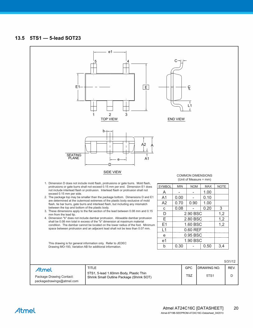
This drawing is for general information only. Refer to JEDEC Drawing MO-193, Variation AB for additional information.
Atmel®, Atmel logo and combinations thereof, Enabling Unlimited Possibilities®, and others are registered trademarks or trademarks of Atmel Corporation or its subsidiaries. Other terms and product names may be trademarks of others.
DISCLAIMER: The information in this document is provided in connection with Atmel products. No license, express or implied, by estoppel or otherwise, to any intellectual property rightis granted by this document or in connection with the sale of Atmel products. EXCEPT AS SET FORTH IN THE ATMEL TERMS AND CONDITIONS OF SALES LOCATED ON THEATMEL WEBSITE, ATMEL ASSUMES NO LIABILITY WHATSOEVER AND DISCLAIMS ANY EXPRESS, IMPLIED OR STATUTORY WARRANTY RELATING TO ITS PRODUCTSINCLUDING, BUT NOT LIMITED TO, THE IMPLIED WARRANTY OF MERCHANTABILITY, FITNESS FOR A PARTICULAR PURPOSE, OR NON-INFRINGEMENT. IN NO EVENTSHALL ATMEL BE LIABLE FOR ANY DIRECT, INDIRECT, CONSEQUENTIAL, PUNITIVE, SPECIAL OR INCIDENTAL DAMAGES (INCLUDING, WITHOUT LIMITATION, DAMAGESFOR LOSS AND PROFITS, BUSINESS INTERRUPTION, OR LOSS OF INFORMATION) ARISING OUT OF THE USE OR INABILITY TO USE THIS DOCUMENT, EVEN IF ATMEL HASBEEN ADVISED OF THE POSSIBILITY OF SUCH DAMAGES. Atmel makes no representations or warranties with respect to the accuracy or completeness of the contents of thisdocument and reserves the right to make changes to specifications and products descriptions at any time without notice. Atmel does not make any commitment to update the informationcontained herein. Unless specifically provided otherwise, Atmel products are not suitable for, and shall not be used in, automotive applications. Atmel products are not intended,authorized, or warranted for use as components in applications intended to support or sustain life.
SAFETY-CRITICAL, MILITARY, AND AUTOMOTIVE APPLICATIONS DISCLAIMER: Atmel products are not designed for and will not be used in connection with any applications wherethe failure of such products would reasonably be expected to result in significant personal injury or death (“Safety-Critical Applications”) without an Atmel officer's specific writtenconsent. Safety-Critical Applications include, without limitation, life support devices and systems, equipment or systems for the operation of nuclear facilities and weapons systems.Atmel products are not designed nor intended for use in military or aerospace applications or environments unless specifically designated by Atmel as military-grade. Atmel products arenot designed nor intended for use in automotive applications unless specifically designated by Atmel as automotive-grade.


![AT24C16C - Microchip Technologyww1.microchip.com/downloads/...AT24C16C-Datasheet.pdf · AT24C16C [DATASHEET] Atmel-8719D-SEEPROM-AT24C16C-Datasheet_122016 4 5. Memory Organization](https://static.documents.pub/doc/80x56/5f05ab717e708231d4141cff/at24c16c-microchip-at24c16c-datasheet-atmel-8719d-seeprom-at24c16c-datasheet122016.jpg)

