An IMPORTANT NOTICE at the end of this data sheet addresses availability, warranty, changes, use in safety-critical applications,intellectual property matters and other important disclaimers. PRODUCTION DATA.
bq25898, bq25898DSLUSCA6B –MARCH 2016–REVISED MARCH 2017
bq25898, bq25898D I2C Controlled Single Cell 4-A Fast Charger with MaxCharge™Technology for High Input Voltage and Adjustable Voltage USB On-the-Go Boost Mode
1
1 Features1• High Efficiency 4-A, 1.5-MHz Switch Mode Buck
Charge– 92% Charge Efficiency at 3 A and 91% Charge
Efficiency at 4 A Charge Current– Optimize for High Voltage Input (9 V / 12 V)– Low Power PFM mode for Light Load
Operations• USB On-the-Go (OTG) with Adjustable Output
from 4.5 V to 5.5 V– Selectable 500-KHz / 1.5-MHz Boost
Converter with up-to 2.4 A Output– 94% Boost Efficiency at 5 V at 1 A Output– Accurate Hiccup Mode Overcurent Protection
• Single Input to Support USB Input and AdjustableHigh Voltage Adapters– Support 3.9-V to 14-V Input Voltage Range– Input Current Limit (100 mA to 3.25 A with 50-
mA resolution) to Support USB2.0, USB3.0standard and High Voltage Adapters
– Maximum Power Tracking by Input VoltageLimit up-to 14V for Wide Range of Adapters
– Auto Detect USB SDP, CDP, DCP, and Non-Standard Adapters (bq25898)
– Programmable D+/D- Drivers for Non-StandardAdapter Handshake
• Remote Battery Sensing• Input Current Optimizer (ICO) to Maximize Input
Power without Overloading Adapters• Resistance Compensation (IRCOMP) from
Charger Output to Cell Terminal• Highest Battery Discharge Efficiency with 5-mΩ
Battery Discharge MOSFET up to 9 A• Integrated ADC for System Monitor
(Voltage, Temperature, Charge Current)• Narrow VDC (NVDC) Power Path Management
– Instant-on Works with No Battery or DeeplyDischarged Battery
– Ideal Diode Operation in Battery SupplementMode
• BATFET Control to Support Ship Mode, Wake Up,and Full System Reset
• Flexible Autonomous and I2C Mode for OptimalSystem Performance
• High Integration includes all MOSFETs, CurrentSensing and Loop Compensation
• 12-µA Low Battery Leakage Current to SupportShip Mode
• High Accuracy– ±0.5% Charge Voltage Regulation– ±5% Charge Current Regulation– ±7.5% Input Current Regulation
• Safety– Battery Temperature Sensing for Charge and
Boost Mode– Thermal Regulation and Thermal Shutdown
• Available in 2.8-mm x 2.5-mm 42-Ball DSBGAPackage
2 Applications• Smart Phone• Tablet PC• Portable Internet Devices
3 DescriptionThe bq25898, bq25898D are highly-integrated 4-Aswitch-mode battery charge management and systempower path management devices for single cell Li-Ionand Li-polymer battery. The devices support highinput voltage fast charging.
Device Information(1)
PART NUMBER PACKAGE BODY SIZE (NOM)bq25898 DSBGA (42) 2.80 mm x 2.50 mmbq25898D DSBGA (42) 2.80 mm x 2.50 mm
(1) For all available packages, see the orderable addendum atthe end of the data sheet.
Simplified Schematic
2
bq25898, bq25898DSLUSCA6B –MARCH 2016–REVISED MARCH 2017 www.ti.com
9.4 Register Map........................................................... 3410 Application and Implementation........................ 51
10.1 Application Information.......................................... 5110.2 Typical Application Diagram ................................. 5110.3 System Example ................................................... 56
11 Power Supply Recommendations ..................... 5712 Layout................................................................... 57
12.1 Layout Guidelines ................................................. 5712.2 Layout Example .................................................... 57
13 Device and Documentation Support ................. 5813.1 Device Support .................................................... 5813.2 Related Links ........................................................ 5813.3 Receiving Notification of Documentation Updates 5813.4 Community Resources.......................................... 5813.5 Trademarks ........................................................... 5813.6 Electrostatic Discharge Caution............................ 5813.7 Glossary ................................................................ 58
14 Mechanical, Packaging, and OrderableInformation ........................................................... 58
4 Revision History
Changes from Revision A (December 2016) to Revision B Page
• Full data sheet to product folder ............................................................................................................................................ 1
Changes from Original (March 2016) to Revision A Page
• Changed 93% to 94% in Features ......................................................................................................................................... 1• Changed anode to cathode in BTST ...................................................................................................................................... 6• Changed cathode to anode in REGN..................................................................................................................................... 6• Changed falling to rising in tACOV_RISING test conditions in Electrical Characteristics .............................................................. 9• Deleted USB SDP (USB100) and the OTG Pin column from Table 3 and Table 4 ............................................................. 19• Changed VREF to VREGN in Equation 2 ........................................................................................................................... 25• Changed VREF to VREGN in Figure 18 ............................................................................................................................. 26• Changed 260 Ω to 232 Ω in Input Current Limit on ILIM ..................................................................................................... 28• Added note to Figure 49 ...................................................................................................................................................... 51
5 Description (Continued)The low impedance power path optimizes switch-mode operation efficiency, reduces battery charging time andextends battery life during discharging phase. The I2C Serial interface with charging and system settings makesthe device a truly flexible solution.
The bq25898/98D is a highly-integrated 4-A switch-mode battery charge management and system power pathmanagement device for single cell Li-Ion and Li-polymer battery. It features fast charging with high input voltagesupport for a wide range of smartphone, tablet and portable devices. Its low impedance power path optimizesswitch-mode operation efficiency, reduces battery charging time and extends battery life during dischargingphase. It also integrates Input Current Optimizer (ICO) and Resistance Compensation (IRCOMP) to delivermaximum charging power to battery. The solution is highly integrated with input reverse-blocking FET (RBFET,Q1), high-side switching FET (HSFET, Q2), low-side switching FET (LSFET, Q3), and battery FET (BATFET, Q4)between system and battery. It also integrates the bootstrap diode for the high-side gate drive and batterymonitor for simplified system design. The I2C serial interface with charging and system settings makes the devicea truly flexible solution.
The device supports a wide range of input sources, including standard USB host port, USB charging port, andUSB compliant adjustable high voltage adapter. To support fast charging using adjustable high voltage adapter,the bq25898D provides support for MaxCharge™ handshake using D+/D- pins and DSEL pin for USB switchcontrol. In addition, both bq25898D and bq25898 include interface to support adjustable high voltage adapterusing input current pulse protocol. To set the default input current limit, device uses the built-in USB interface(bq25898D) or takes the result from detection circuit in the system (bq25898), such as USB PHY device. Thedevice is compliant with USB 2.0 and USB 3.0 power spec with input current and voltage regulation. In addition,the Input Current Optimizer (ICO) supports the detection of maximum power point detection of the input sourcewithout overload. The device also meets USB On-the-Go (OTG) operation power rating specification bysupplying 5 V (Adjustable 4.5V-5.5V) on VBUS with current limit up to 2.4 A.
The power path management regulates the system slightly above battery voltage but does not drop below 3.5Vminimum system voltage (programmable). With this feature, the system maintains operation even when thebattery is completely depleted or removed. When the input current limit or voltage limit is reached, the powerpath management automatically reduces the charge current to zero. As the system load continues to increase,the power path discharges the battery until the system power requirement is met. This operation preventsoverloading the input source.
The device initiates and completes a charging cycle without software control. It automatically detects the batteryvoltage and charges the battery in three phases: pre-conditioning, constant current and constant voltage. At theend of the charging cycle, the charger automatically terminates when the charge current is below a preset limit inthe constant voltage phase. When the full battery falls below the recharge threshold, the charger willautomatically start another charging cycle.
The charger provides various safety features for battery charging and system operations, including batterytemperature negative thermistor monitoring, charging safety timer and overvoltage/overcurrent protections. Thethermal regulation reduces charge current when the junction temperature exceeds 120°C (programmable). TheSTAT output reports the charging status and any fault conditions. The PG output (bq25898) indicates if a goodpower source is present. The INT immediately notifies host when fault occurs.
The device also provides a 7-bit analog-to-digital converter (ADC) for monitoring charge current andinput/battery/system (VBUS, BAT, SYS, TS) voltages. The QON pin provides BATFET enable/reset control toexit low power ship mode or full system reset function.
The devices are available in a 42-ball, 2.8 mm x 2.5 mm DSBGA package.
(1) DI (Digital Input), DO (Digital Output), DIO (Digital Input/Output), AI (Analog Input), AO (Analog Output), AIO (Analog Input/Output)
Pin FunctionsPIN
TYPE (1) DESCRIPTIONNAME bq25898 bq25898D
VBUS E3-G3 E3-G3 PCharger Input Voltage. The internal n-channel reverse block MOSFET (RBFET) is connectedbetween VBUS and PMID with VBUS on source. Place a 1-µF ceramic capacitor from VBUS toPGND and place it as close as possible to IC.
D+ – C3 AIOPositive line of the USB data line pair. D+/D- based USB host/charging port detection. Thedetection includes data contact detection (DCD), primary and secondary detection in BC1.2, andAdjustable high voltage adapter.
PSEL C3 – DI Power source selection input. High indicates a USB host source and Low indicates an adaptersource.
D– – D3 AIONegative line of the USB data line pair. D+/D- based USB host/charging port detection. Thedetection includes data contact detection (DCD), primary and secondary detection in BC1.2, andAdjustable high voltage adapter.
PG D3 – DOOpen drain active low power good indicator. Connect to the pull up rail via 10-kΩ resistor. LOWindicates a good input source if the input voltage is within VVBUS_OP, above SLEEP mode threshold(VSLEEPZ), and current limit is above IBATSRC(30 mA).
STAT G1 G1 DO
Open drain charge status output to indicate various charger operation. Connect to the pull up railvia 10-kΩ resistor. LOW indicates charge in progress. HIGH indicates charge complete or chargedisabled. When any fault condition occurs, STAT pin blinks in 1 Hz. The STAT pin function can bedisabled when STAT_DIS bit is set.
SCL A3 A3 DI I2C Interface clock. Connect SCL to the logic rail through a 10-kΩ resistor.
SDA B3 B3 DIO I2C Interface data. Connect SDA to the logic rail through a 10-kΩ resistor.
INT F2 F2 DO Open-drain Interrupt Output. Connect the INT to a logic rail via 10-kΩ resistor. The INT pin sendsactive low, 256-μs pulse to host to report charger device status and fault.
OTG C4 C4 DIActive high enable pin during boost mode. Deleted text form the OTG pin Description "OTG = High,IINLIM is set to USB500 mode". The boost mode is activated when OTG_CONFIG =1 and OTG pinis highChanged the Description of the OTG pin in the Pin Functions table.
CE B4 B4 DI Active low Charge Enable pin. Battery charging is enabled when CHG_CONFIG = 1 and CE pin =Low. CE pin must be pulled High or Low.
ILIM G2 G2 AI
Input current limit Input. ILIM pin sets the maximum input current and can be used to monitor inputcurrent ILIM pin sets the maximum input current limit by regulating the ILIM voltage at 0.8 V. Aresistor is connected from ILIM pin to ground to set the maximum limit as IINMAX = KILIM/RILIM. Theactual input current limit is the lower limit set by ILIM pin (when EN_ILIM bit is high) or IIINLIMregister bits. Input current limit of less than 500 mA is not support on ILIM pin. ILIM pin can also beused to monitor input current when the voltage is below 0.8V. The input current is proportional tothe voltage on ILIM pin and can be calculated by IIN = (KILIM x VILIM) / (RILIM x 0.8) The ILIM pinfunction can be disabled when EN_ILIM bit is 0.
TS A4 A4 AITemperature qualification voltage input. Connect a negative temperature coefficient thermistor.Program temperature window with a resistor divider from REGN to TS to GND. Charge suspendswhen either TS pin is out of range. Recommend 103AT-2 thermistor.
QON B6 B6 DI
BATFET enable/reset control input. When BATFET is in ship mode, a logic low of tSHIPMODE (typical1sec) duration turns on BATFET to exit shipping mode. . When VBUS is not plugged-in, a logic lowof tQON_RST (typical 19.5sec) duration resets SYS (system power) by turning BATFET off fortBATFET_RST (typical 0.325sec) and then re-enable BATFET to provide full system power reset. Thepin contains an internal pull-up to maintain default high logic
BAT A1-E1 A1-E1 P Battery connection point to the positive terminal of the battery pack. The internal BATFET isconnected between BAT and SYS. Connect a 10uF closely to the BAT pin.
SYS A2-E2 A2-E2 PSystem connection point. The internal BATFET is connected between BAT and SYS. When thebattery falls below the minimum system voltage, switch-mode converter keeps SYS above theminimum system voltage. Connect a 20uF closely to the SYS pin.
PGND C6-G6 C6-G6 P Power ground connection for high-current power converter node.
SW C5-G5 C5-G5 PSwitching node connecting to output inductor. Internally SW is connected to the source of the n-channel HSFET and the drain of the n-channel LSFET. Connect the 0.047μF bootstrap capacitorfrom SW to BTST.
BTST A6 A6 P PWM high side driver positive supply. Internally, the BTST is connected to the cathode of theboost-strap diode. Connect the 0.047μF bootstrap capacitor from SW to BTST.
REGN A5 A5 PPWM low side driver positive supply output. Internally, REGN is connected to the anode of theboost-strap diode. Connect a 4.7 µF (10 V rating) ceramic capacitor from REGN to analog GND.The capacitor should be placed close to the IC. REGN also serves as bias rail of TS pin.
PMID D4-G44 D4-G4 DOConnected to the drain of the reverse blocking MOSFET (RBFET) and the drain of HSFET. Giventhe total input capacitance, put 1µF on VBUS to PGND, and the rest capacitance on PMID toPGND.
DSEL – B5 DO
Active high D+/D- multiplexer selection control. Connect a 47-nF (6V rating) ceramic capacitor fromDSEL to analog GND. The pin is normally low. During input source type detection, the pin driveshigh to indicate the bq25890 D+/D- detection is in progress and needs to take control of D+, D-signals. When detection is completed, the pin keeps high when DCP, MaxCharge or HVDCP isdetected. The pin returns to low when other input source type is detected
VOK B5 – DO LDO output to driver USB PHY/MUX. Connect a 47nF ceramic capacitor from VOK to analog GND.
BATSEN F1 F1 AI Remote battery sense input. The typical pin resistance is 800 kΩ. Connect as close to battery aspossible.
(1) Stresses beyond those listed under absolute maximum ratings may cause permanent damage to the device. These are stress ratingsonly, and functional operation of the device at these or any other conditions beyond those indicated under recommended operatingconditions is not implied. Exposure to absolute-maximum-rated conditions for extended periods may affect device reliability. All voltagevalues are with respect to the network ground terminal unless otherwise noted.
8 Specifications
8.1 Absolute Maximum Ratings (1)
over operating free-air temperature range (unless otherwise noted)MIN MAX VALUE
Voltage range (with respect to GND)
VBUS (converter not switching) –2 22 VPMID (converter not switching) –0.3 22 VSTAT –0.3 20 VPG (bq25898) –0.3 7 VPSEL (bq25898) –0.3 7 VVOK (bq25898) –0.3 7 VDSEL (bq25898D) –0.3 7 VD+, D– (bq25898D) –0.3 7 VBTST –0.3 20 VSW –3 16 VBAT, SYS (converter not switching) –0.3 6 VSDA, SCL, INT, OTG, REGN, TS, CE, QON –0.3 7 VBTST TO SW –0.3 7 VPGND to GND –0.3 0.3 VBATSEN –0.3 7 VILIM –0.3 5 V
Output sink current
INT, STAT 6 mAPG (bq25898) 6 mADSEL (bq25898D) 5 mAVOK (bq25898) 5 mA
Junction temperature –40 150 °CStorage temperature range, Tstg –65 150 °C
(1) JEDEC document JEP155 states that 500-V HBM allows safe manufacturing with a standard ESD control process.(2) JEDEC document JEP157 states that 250-V CDM allows safe manufacturing with a standard ESD control process.
8.2 ESD RatingsVALUE UNIT
VESD Electrostatic dischargeHuman body model (HBM), per ANSI/ESDA/JEDEC JS-001 (1) ±2000 VCharged device model (CDM), per JEDEC specificationJESD22-C101 (2) ±250 V
(1) The inherent switching noise voltage spikes should not exceed the absolute maximum rating on either the BTST or SW pins. A tightlayout minimizes switching noise.
8.3 Recommended Operating ConditionsMIN MAX UNIT
VIN Input voltage 3.9 14 (1) VIIN Input current (VBUS) 3.25 AISYS Output current (SW) 4 AVBAT Battery voltage 4.608 V
IBAT
Fast charging current 4 A
Discharging current with internal MOSFETUp to 6 (continuos) A
9 (peak)(Up to 1 sec duration) A
TA Operating free-air temperature range –40 85 °C
(1) For more information about traditional and new thermal metrics, see the Semiconductor and IC Package Thermal Metrics applicationreport.
Electrical Characteristics (continued)VVBUS_UVLOZ < VVBUS < VACOV and VVBUS > VBAT + VSLEEP, TJ = –40°C to 125°C and TJ = 25°C for typical values (unlessotherwise noted)
PARAMETER TEST CONDITIONS MIN TYP MAX UNIT
BAT OVER-VOLTAGE/CURRENT PROTECTION
VBAT(OVP) Battery over-voltage threshold VBAT rising, as percentage of VBAT(REG) 104%
VBAT(OVP_HYST) Battery over-voltage hysteresis VBAT falling, as percentage of VBAT(REG) 2%
IBAT(FET_OCP) System over-current threshold 9 A
THERMAL REGULATION AND THERMAL SHUTDOWN
TREG Junction temperature regulation accuracy REG08[1:0] = 11 120 °C
TSHUT Thermal shutdown rising temperature Temperature rising 160 °C
TSHUT(HYS) Thermal shutdown hysteresis Temperature falling 30 °C
JEITA THERMISTOR COMPARATOR (BUCK MODE)
V(T1)T1 (0°C) threshold, charge suspended T1 below thistemperature. As percentage to V(REGN) 72.75% 73.25% 73.75%
V(T1_HYS)Charge back to ICHG/2 (REG04[6:0]) and VREG (REG06[7:2])above this temperature. As Percentage to V(REGN) 1.4%
V(T2)T2 (10°C) threshold, charge back to ICHG/2 (REG04[6:0]) andVREG (REG06[7:2]) below this temperature. As Percentage to V(REGN) 67.75% 68.25% 68.75%
V(T2_HYS)Charge back to ICHG (REG04[6:0]) and VREG (REG06[7:2])above this temperature. As Percentage to V(REGN) 1.4%
V(T3)T3 (45°C) threshold,charge back to ICHG (REG04[6:0]) andVREG-200mV (REG06[7:2]) above this temperature. As percentage to V(REGN) 44.25v 44.75% 45.25%
V(T3_HYS)Charge back to ICHG (REG04[6:0]) and VREG (REG06[7:2])below this temperature. As Percentage to V(REGN) 1%
V(T5)T5 (60°C) threshold, charge suspended above thistemperature. As Percentage to V(REGN) 33.875% 34.375% 34.875%
V(T5_HYS)Charge back to ICHG (REG04[6:0]) and VREG-200mV(REG06[7:2]) below this temperature. As Percentage to V(REGN) 1.25%
COLD/HOT THERMISTOR COMPARATOR (BOOST MODE)
V(BCOLD1) Cold temperature threshold 1, TS pin voltage rising threshold As percentage to VREGN REG01[5] = 1(Approx. -20°C w/ 103AT) 79.5% 80% 80.5%
V(BCOLD1_HYS) Cold temperature threshold 1, TS pin voltage falling threshold As percentage to VREGN REG01[5] = 1 1%
V(BHOT2) Hot temperature threshold 2, TS pin voltage falling threshold As percentage to VREGN REG01[7:6] = 10(Approx. 65°C w/ 103AT) 30.75% 31.25% 31.75%
V(BHOT2_HYS) Hot temperature threshold 2, TS pin voltage rising threshold As percentage to VREGN REG01[7:6] = 10 3%
PWM
FSW PWM switching frequency, and digital clock Oscillator frequency 1.32 1.68 MHz
DMAX Maximum PWM duty cycle 97%
BOOST MODE OPERATION
V(OTG_REG_RANGE) Typical boost mode regulation voltage range 4.55 5.55 V
V(OTG_REG_STEP) Typical boost Mode Regulation voltage step 64 mV
V(OTG_REG_ACC) Boost mode regulation voltage accuracy I(VBUS) = 0 A, BOOSTV = 4.998 V(REG0A[7:4] = 0111) -3% 3%
V(OTG_BAT) Battery voltage exiting boost modeBAT falling, REG03[0] = 0 2.7 2.9 V
BAT falling, REG03[0] = 1 2.4 2.6 V
I(OTG) Typical boost mode output current range 0.5 2.45 A
I(OTG_OCP_ACC) Boost mode RBFET over-current protection accuracy BOOST_LIM = 1.5 A (REG0A[2:0] = 100) 1.5 2.0 A
V(OTG_OVP) Boost mode over-voltage threshold Rising threshold 5.8 6 V
REGN LDO
V(REGN) REGN LDO output voltageV(VBUS) = 9 V, I(REGN) = 40 mA 5.6 6 6.4 V
V(VBUS) = 5 V, I(REGN) = 20 mA 4.7 4.8 V
I(REGN) REGN LDO current limit V(VBUS) = 9 V, V(REGN) = 3.8 V 50 mA
ANALOG-TO-DIGITAL CONVERTER (ADC)
RES Resolution Rising threshold 7 bits
VBAT(RANGE) Typical battery voltage range
V(VBUS) > VBAT + V(SLEEP) or OTG mode isenabled 2.304 4.848 V
V(VBUS) < VBAT + V(SLEEP) and OTG mode isdisabled VSYS_MIN 4.848 V
V(BAT_RES) Typical battery voltage resolution 20 mV
Electrical Characteristics (continued)VVBUS_UVLOZ < VVBUS < VACOV and VVBUS > VBAT + VSLEEP, TJ = –40°C to 125°C and TJ = 25°C for typical values (unlessotherwise noted)
PARAMETER TEST CONDITIONS MIN TYP MAX UNIT
V(SYS_RANGE) Typical system voltage range
V(VBUS) > VBAT + V(SLEEP) or OTG mode isenabled 2.304 4.848 V
V(VBUS) < VBAT + V(SLEEP) and OTG mode isdisabled VSYS_MIN 4.848 V
V(SYS_RES) Typical system voltage resolution 20 mV
V(VBUS_RANGE) Typical VVBUS voltage range V(VBUS) > VBAT + V(SLEEP) or OTG mode isenabled 2.6 15.3 V
V(VBUS_RES) Typical VVBUS voltage resolution 100 mV
IBAT(RANGE) Typical battery charge current range V(VBUS) > VBAT + V(SLEEP) and VBAT >VBAT(SHORT)
0 4.032 A
IBAT(RES) Typical battery charge current resolution 50 mA
V(TS_RANGE) Typical TS voltage range 21% 80%
V(TS_RES) Typical TS voltage resolution 0.47%
LOGIC I/O PIN (OTG, CE, PSEL, QON)
VIH Input high threshold level 1.3 V
VIL Input low threshold level 0.4 V
IIN(BIAS) High level leakage current Pull-up rail 1.8 V 1 µA
V(QON) Internal /QON pull-up
Battery only mode BAT V
V(VBUS) = 9 V 5.8 V
V(VBUS) = 5 V 4.3 V
R(QON) Internal /QON pull-up resistance 200 kΩ
LOGIC I/O PIN (INT, STAT, PG)
VOL Output low threshold level Sink Current = 5 mA, Sink current 0.4 V
IOUT_BIAS High level leakage current Pull-up rail 1.8 V 1 µA
I2C INTERFACE (SCL, SDA)
VIH Input high threshold level, SCL and SDA Pull-up rail 1.8 V 1.3 V
VIL Input low threshold level Pull-up rail 1.8 V 0.4 V
VOL Output low threshold level Sink Current = 5 mA, Sink current 0.4 V
IBIAS High level leakage current Pull-up rail 1.8 V 1 µA
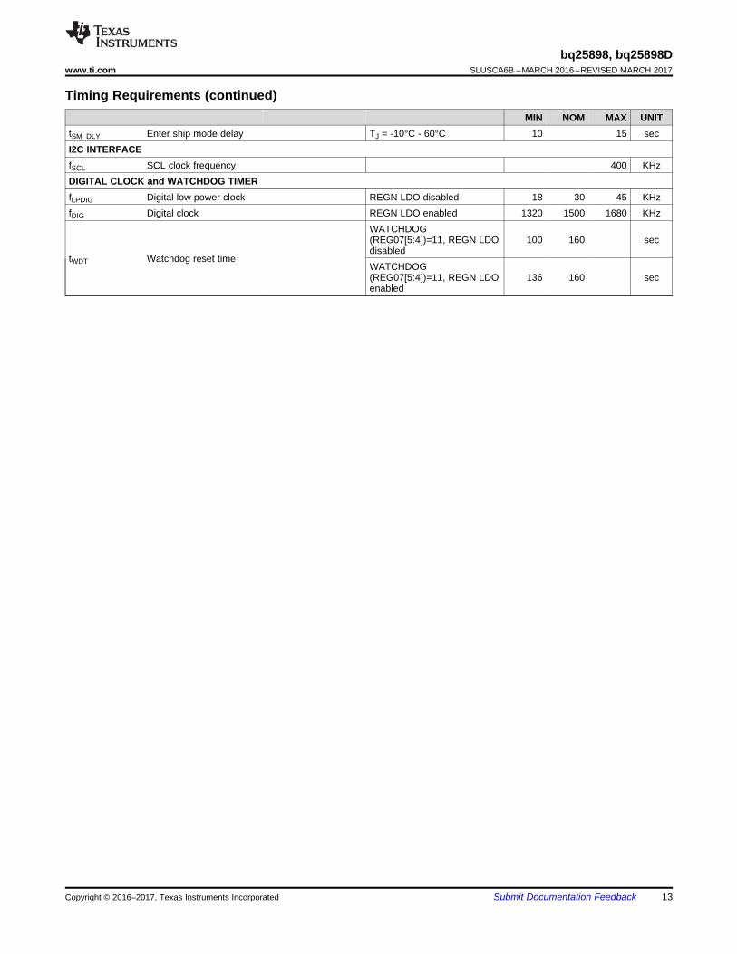
8.6 Timing RequirementsMIN NOM MAX UNIT
VBUS/BAT POWER UPtBADSRC Bad adapter detection duration 30 msecBAT OVER-VOLTAGE PROTECTION
tBATOVPBattery over-voltage deglitch time to disablecharge 1 µs
BATTERY CHARGERtRECHG Recharge deglitch time 20 msecCurrent Pulse ControltPUMPX_STOP Current pulse control stop pulse 430 570 msectPUMPX_ON1 Current pulse control long on pulse 240 360 msectPUMPX_ON2 Current pulse control short on pulse 70 130 msectPUMPX_OFF Current pulse control off pulse 70 130 msectPUMPX_DLY Current pulse control stop start delay 80 225 msecBATTERY MONITORtCONV Conversion time CONV_RATE(REG02[6]) = 0 8 1000 msecQON and SHIPMODE TIMING
tSHIPMODEQON low time to turn on BATFET and exit shipmode TJ = -10°C - 60°C 0.8 1.3 sec
tQON_RST QON low time to enable full system reset TJ = -10°C - 60°C 15.5 23 sectBATFET_RST BATFET off time during full system reset TJ = -10°C - 60°C 250 400 msec
9 Detailed DescriptionThe device is a highly integrated 4-A switch-mode battery charger for single cell Li-Ion and Li-polymer battery. Itis highly integrated with the input reverse-blocking FET (RBFET, Q1), high-side switching FET (HSFET, Q2) ,low-side switching FET (LSFET, Q3), and battery FET (BATFET, Q4). The device also integrates the boostrapdiode for the high-side gate drive.
9.2.1 Device Power-On-Reset (POR)The internal bias circuits are powered from the higher voltage of VBUS and BAT. When VBUS rises aboveVVBUS_UVLOZ or BAT rises above VBAT_UVLOZ , the sleep comparator, battery depletion comparator and BATFETdriver are active. I2C interface is ready for communication and all the registers are reset to default value. Thehost can access all the registers after POR.
9.2.2 Device Power Up from Battery without Input SourceIf only battery is present and the voltage is above depletion threshold (VBAT_DPLZ), the BATFET turns on andconnects battery to system. The REGN LDO stays off to minimize the quiescent current. The low RDS(ON) ofBATFET and the low quiescent current on BAT minimize the conduction loss and maximize the battery run time.The device always monitors the discharge current through BATFET (see Supplement Mode). When the system isoverloaded or shorted (IBAT > IBATFET_OCP), the device turns off BATFET immediately and sets BATFET_DIS bitto indicate BATFET is disabled until the input source plugs in again or one of the methods describe in BATFETEnable (Exit Shipping Mode) is applied to re-enable BATFET.
9.2.3 Device Power Up from Input SourceWhen an input source is plugged in, the device checks the input source voltage to turn on REGN LDO and all thebias circuits. It detects and sets the input current limit before the buck converter is started whenAUTO_DPDM_EN bit is set. The power up sequence from input source is as listed:1. Power Up REGN LDO2. Poor Source Qualification3. Input Source Type Detection based on D+/D- (bq25898D) or PSEL (bq25898) to set default Input Current
Limit (IINLIM) register and input source type4. Input Voltage Limit Threshold Setting (VINDPM threshold)5. Converter Power-up
9.2.3.1 Power Up REGN Regulation (LDO)The REGN LDO supplies internal bias circuits as well as the HSFET and LSFET gate drive. The LDO alsoprovides bias rail to TS external resistors. The pull-up rail of STAT and PG can be connected to REGN as well.The REGN is enabled when all the below conditions are valid.1. VBUS above VVBUS_UVLOZ
2. VBUS above VBAT + VSLEEPZ in buck mode or VBUS below VBAT + VSLEEP in boost mode3. After 220 ms delay is completed
If one of the above conditions is not valid, the device is in high impedance mode (HIZ) with REGN LDO off. Thedevice draws less than IVBUS_HIZ from VBUS during HIZ state. The battery powers up the system when the deviceis in HIZ.
9.2.3.2 Poor Source QualificationAfter REGN LDO powers up, the device checks the current capability of the input source. The input source hasto meet the following requirements in order to start the buck converter.1. VBUS voltage below VACOV
2. VBUS voltage above VVBUSMIN when pulling IBADSRC (typical 30mA)
Once the input source passes all the conditions above, the status register bit VBUS_GD is set high and the INTpin is pulsed to signal to the host. If the device fails the poor source detection, it repeats poor source qualificationevery 2 seconds.
9.2.3.3 Input Source Type DetectionAfter the VBUS_GD bit is set and REGN LDO is powered, the charger device runs Input Source Type Detectionwhen AUTO_DPDM_EN bit is set.
Feature Description (continued)The bq25898D follows the USB Battery Charging Specification 1.2 (BC1.2) and to detect input source(SDP/CDP/DCP) and non-standard adapter through USB D+/D- lines. In addition, when USB DCP is detected, itinitiates adjustable high voltage adapter handshake on D+/D-. The device supports MaxCharge™ handshakewhen MAXC_EN or HVDCP_EN is set. The bq25898 sets input current limit through PSEL and OTG pins.
After input source type detection, an INT pulse is asserted to the host. In addition, the following registers and pinare changed:1. Input Current Limit (IINLIM) register is changed to set current limit2. PG_STAT bit is set3. PG pin goes low (bq25898)
The host can over-write IINLIM register to change the input current limit if needed. The charger input current isalways limited by the lower of IINLIM register or ILIM pin at all-time regardless of Input Current Optimizer (ICO) isenable or disabled.
When AUTO_DPDM_EN is disabled, the Input Source Type Detection is bypassed. The Input Current Limit(IINLIM) register, VBUS_STAT, and SPD_STAT bits are unchanged from previous values.
9.2.3.3.1 D+/D– Detection Sets Input Current Limit (bq25898D)
The bq25898D contains a D+/D– based input source detection to set the input current limit automatically. TheD+/D- detection includes standard USB BC1.2, non-standard adapter, and adjustable high voltage adapterdetections. When input source is plugged-in, the device starts standard USB BC1.2 detections. The USB BC1.2is capable to identify Standard Downstream Port (SDP), Charging Downstream Port (CDP), and DedicatedCharging Port (DCP). When the Data Contact Detection (DCD) timer of 500ms is expired, the non-standardadapter detection is applied to set the input current limit.
When DCP is detected, the device initates adjustable high voltage adapter handshake including MaxCharge™,etc. The handshake connects combinations of voltage source(s) and/or current sink on D+/D- to signal inputsource to raise output voltage from 5 V to 9 V / 12 V. The adjustable high voltage adapter handshake can bedisabled by clearing MAXC_EN and/or HVDCP_EN bits .
ADAPTER D+ THRESHOLD D- THRESHOLD INPUT CURRENT LIMIT
Divider 1 VD+ within V2P7_VTH VD- within V2P0_VTH 2.1ADivider 2 VD+ within V1P2_VTH VD- within V1P2_VTH 2ADivider 3 VD+ within V2P0_VTH VD- within V2P7_VTH 1ADivider 4 VD+ within V2P7_VTH VD- within V2P7_VTH 2.4A
Table 2. Adjustable High Voltage Adapter D+/D- Output ConfigurationsADJUSTABLE HIGH VOLTAGE
After the Input Source Type Detection is done, an INT pulse is asserted to the host. In addition, the followingregisters including Input Current Limit register (IINLIM), VBUS_STAT, and SDP_STAT are updated as below:
Table 3. bq25898D Result
D+/D- DETECTION INPUT CURRENT LIMIT(IINLIM) SDP_STAT VBUS_STAT
USB SDP (USB500) 500 mA 1 001USB CDP 1.5 A 1 010USB DCP 3.25 A 1 011Divider 3 1 A 1 110Divider 1 2.1 A 1 110Divider 4 2.4 A 1 110Divider 2 2 A 1 110
MaxCharge 1.5 A 1 100Unknown Adapter 500 mA 1 101
9.2.3.3.2 PSEL Pin Sets Input Current Limit (bq25898)
The bq25898 has PSEL interface for input current limit setting to interface with USB PHY. It directly takes theUSB PHY device output to decide whether the input is USB host or charging port. To implement USB100 in thesystem, the host can enter HiZ mode by setting EN_HIZ bit after 2 min charging with 500 mA input current limit.
Table 4. bq25898 Result
INPUT DETECTION BAT VOLTAGE PSEL PIN INPUT CURRENT LIMIT(IINLIM) SDP_STAT VBUS_STAT
USB SDP (USB500) X High 500 mA 1 001Adapter X Low 3.25 A 1 010
9.2.3.3.3 Force Input Current Limit Detection
In host mode, the host can force the device to run by setting FORCE_DPDM bit. After the detection is completed,FORCE_DPDM bit returns to 0 by itself and Input Result is updated.
9.2.3.4 Input Voltage Limit Threshold Setting (VINDPM Threshold)The device supports wide range of input voltage limit (3.9 V – 14 V) for high voltage charging and provides twomethods to set Input Voltage Limit (VINDPM) threshold to facilitate autonomous detection.1. Absolute VINDPM (FORCE_VINDPM=1)
By setting FORCE_VINDPM bit to 1, the VINDPM threshold setting algorithm is disabled. Register VINDPMis writable and allows host to set the absolute threshold of VINDPM function.
2. Relative VINDPM based on VINDPM_OS registers (FORCE_VINDPM=0) (Default)
When FORCE_VINDPM bit is 0 (default), the VINDPM threshold setting algorithm is enabled. The VINDPMregister is read only and the charger controls the register by using VINDPM Threshold setting algorithm. Thealgorithm allows a wide range of adapter (VVBUS_OP) to be used with flexible VINDPM threshold.
After Input Voltage Limit Threshold is set, an INT pulse is generated to signal to the host.
9.2.3.5 Converter Power-UpAfter the input current limit is set, the converter is enabled and the HSFET and LSFET start switching. If batterycharging is disabled, BATFET turns off. Otherwise, BATFET stays on to charge the battery.
The device provides soft-start when system rail is ramped up. When the system rail is below 2.2 V, the inputcurrent limit is forced to the lower of 200 mA or IINLIM register setting. After the system rises above 2.2 V, thedevice limits input current to the lower value of ILIM pin and IILIM register (ICO_EN = 0) or IDPM_LIM register(ICO_EN = 1).
As a battery charger, the device deploys a highly efficient 1.5 MHz step-down switching regulator. The fixedfrequency oscillator keeps tight control of the switching frequency under all conditions of input voltage, batteryvoltage, charge current and temperature, simplifying output filter design.
A type III compensation network allows using ceramic capacitors at the output of the converter. An internal saw-tooth ramp is compared to the internal error control signal to vary the duty cycle of the converter. The rampheight is proportional to the PMID voltage to cancel out any loop gain variation due to a change in input voltage.
In order to improve light-load efficiency, the device switches to PFM control at light load when battery is belowminimum system voltage setting or charging is disabled. During the PFM operation, the switching duty cycle isset by the ratio of SYS and VBUS.
9.2.4 Input Current Optimizer (ICO)The device provides innovative Input Current Optimizer (ICO) to identify maximum power point without overloadthe input source. The algorithm automatically identify maximum input current limit of power source withoutentering VINDPM to avoid input source overload.
This feature is enabled by default (ICO_EN=1) and can be disabled by setting ICO_EN bit to 0. After DCP orMaxCharge type input source is detected based on the procedures previously described (Input Source TypeDetection ). The algorithm runs automatically when ICO_EN bit is set. The algorithm can also be forced toexecute by setting FORCE_ICO bit regardless of input source type detected.
The actual input current limit used by the Dynamic Power Management is reported in IDPM_LIM register whileInput Current Optimizer is enabled (ICO_EN = 1) or set by IINLIM register when the algorithm is disabled(ICO_EN = 0). In addition, the current limit is clamped by ILIM pin unless EN_ILIM bit is 0 to disable ILIM pinfunction.
9.2.5 Boost Mode Operation from BatteryThe device supports boost converter operation to deliver power from the battery to other portable devicesthrough USB port. The boost mode output current rating meets the USB On-The-Go 500 mA (BOOST_LIM bits =000) output requirement. The maximum output current is up to 2.4 A. The boost operation can be enabled if theconditions are valid:1. BAT above BATLOWV
2. VBUS less than BAT+VSLEEP (in sleep mode)3. Boost mode operation is enabled (OTG pin HIGH and OTG_CONFIG bit =1)4. Voltage at TS (thermistor) pin is within range configured by Boost Mode Temperature Monitor as configured
by BHOT and BCOLD bits5. After 30 ms delay from boost mode enable
In boost mode, the device employs a 500 KHz or 1.5 MHz (selectable using BOOST_FREQ bit) step-upswitching regulator based on system requirements. To avoid frequency change during boost mode operations,write to boost frequency configuration bit (BOOST_FREQ) is ignored when OTG_CONFIG is set.
During boost mode, the status register VBUS_STAT bits is set to 111, the VBUS output is 5V by default(selectable via BOOSTV register bits) and the output current can reach up to 2.4 A, selected via I2C(BOOST_LIM bits). The boost output is maintained when BAT is above VOTG_BAT threshold.
9.2.6 Power Path ManagementThe device accommodates a wide range of input sources from USB, wall adapter, to car battery. The deviceprovides automatic power path selection to supply the system (SYS) from input source (VBUS), battery (BAT), orboth.
9.2.6.1 Narrow VDC ArchitectureThe device deploys Narrow VDC architecture (NVDC) with BATFET separating system from battery. Theminimum system voltage is set by SYS_MIN bits. Even with a fully depleted battery, the system is regulatedabove the minimum system voltage (default 3.5 V).
When the battery is below minimum system voltage setting, the BATFET operates in linear mode (LDO mode),and the system is regulated above the minimum system voltage setting. As the battery voltage rises above theminimum system voltage, BATFET is fully on and the voltage difference between the system and battery is theVDS of BATFET. The status register VSYS_STAT bit goes high when the system is in minimum system voltageregulation.
Figure 12. V(SYS) vs V(BAT)
9.2.6.2 Dynamic Power ManagementTo meet maximum current limit in USB spec and avoid over loading the adapter, the device features DynamicPower Management (DPM), which continuously monitors the input current and input voltage. When input sourceis over-loaded, either the current exceeds the input current limit (IINLIM or IDPM_LIM) or the voltage falls belowthe input voltage limit (VINDPM). The device then reduces the charge current until the input current falls belowthe input current limit and the input voltage rises above the input voltage limit.
When the charge current is reduced to zero, but the input source is still overloaded, the system voltage starts todrop. Once the system voltage falls below the battery voltage, the device automatically enters the SupplementMode where the BATFET turns on and battery starts discharging so that the system is supported from both theinput source and battery.
During DPM mode, the status register bits VDPM_STAT (VINDPM) and/or IDPM_STAT (IINDPM) is/are set high.Figure 13 shows the DPM response with 9V/1.2A adapter, 3.2-V battery, 2.8-A charge current and 3.4-Vminimum system voltage setting.
9.2.6.3 Supplement ModeWhen the system voltage falls below the battery voltage, the BATFET turns on and the BATFET gate isregulated the gate drive of BATFET so that the minimum BATFET VDS stays at 30 mV when the current is low.This prevents oscillation from entering and exiting the Supplement Mode. As the discharge current increases, theBATFET gate is regulated with a higher voltage to reduce RDS(ON) until the BATFET is in full conduction. At thispoint onwards, the BATFET VDS linearly increases with discharge current. Figure 14 shows the V-I curve of theBATFET gate regulation operation. BATFET turns off to exit Supplement Mode when the battery is below batterydepletion threshold.
Figure 14. BATFET V-I Curve
9.2.7 Battery Charging ManagementThe device charges 1-cell Li-Ion battery with up to 4-A charge current for high capacity battery. The 5-mΩBATFET improves charging efficiency and minimize the voltage drop during discharging.
9.2.7.1 Autonomous Charging CycleWith battery charging enabled (CHG_CONFIG bit = 1 and CE pin is low), the device autonomously completes acharging cycle without host involvement. The device default charging parameters are listed in Table 5. The hostcan always control the charging operations and optimize the charging parameters by writing to the correspondingregisters through I2C.
Table 5. Charging Parameter Default SettingDEFAULT MODE bq25898D bq25898Charging Voltage 4.208 V 4.208 VCharging Current 2.048 A 2.048 A
Pre-charge Current 128 mA 128 mATermination Current 256 mA 256 mATemperature Profile JEITA JEITA
Safety Timer 12 hour 12 hour
A new charge cycle starts when the following conditions are valid:• Converter starts• Battery charging is enabled by setting CHG_CONFIG bit, /CE pin is low and ICHG register is not 0 mA• No thermistor fault on TS pin• No safety timer fault• BATFET is not forced to turn off (BATFET_DIS bit = 0)
The charger device automatically terminates the charging cycle when the charging current is below terminationthreshold, charge voltage is above recharge threshold, and device not in DPM mode or thermal regulation. Whena full battery voltage is discharged below recharge threshold (threshold selectable via VRECHG bit), the deviceautomatically starts a new charging cycle. After the charge is done, either toggle CE pin or CHG_CONFIG bitcan initiate a new charging cycle.
The STAT output indicates the charging status of charging (LOW), charging complete or charge disable (HIGH)or charging fault (Blinking). The STAT output can be disabled by setting STAT_DIS bit. In addition, the statusregister (CHRG_STAT) indicates the different charging phases: 00-charging disable, 01-precharge, 10-fastcharge (constant current) and constant voltage mode, 11-charging done. Once a charging cycle is completed, anINT is asserted to notify the host.
9.2.7.2 Battery Charging ProfileThe device charges the battery in three phases: preconditioning, constant current and constant voltage. At thebeginning of a charging cycle, the device checks the battery voltage and regulates current / voltage.
Table 6. Charging Current SettingVBAT CHARGING CURRENT REG DEFAULT SETTING CHRG_STAT< 2 V IBATSHORT – 01
2 V – 3 V IPRECHG 0 mA (precharge disabled) 01> 3 V ICHG 2048 mA 10
If the charger device is in DPM regulation or thermal regulation during charging, the charging current can be lessthan the programmed value. In this case, termination is temporarily disabled and the charging safety timer iscounted at half the clock rate.
Figure 15. Battery Charging Profile
9.2.7.3 Charging TerminationThe device terminates a charge cycle when the battery voltage is above recharge threshold, and the current isbelow termination current. After the charging cycle is completed, the BATFET turns off. The converter keepsrunning to power the system, and BATFET can turn on again to engage Supplement Mode.
When termination occurs, the status register CHRG_STAT is set to 11, and an INT pulse is asserted to the host.Termination is temporarily disabled when the charger device is in input current, voltage or thermal regulation.Termination can be disabled by writing 0 to EN_TERM bit prior to charge termination.
9.2.7.4 Resistance Compensation (IRCOMP)For high current charging system, resistance between charger output and battery cell terminal such as boardrouting, connector, MOSFETs and sense resistor can force the charging process to move from constant currentto constant voltage too early and increase charge time. To speed up the charging cycle, the device providesresistance compensation (IRCOMP) feature which can extend the constant current charge time to deliverymaximum power to battery.
The device allows the host to compensate for the resistance by increasing the voltage regulation set point basedon actual charge current and the resistance as shown below. For safe operation, the host should set themaximum allowed regulation voltage register (VCLAMP) and the minimum resistance compensation (BATCOMP).
VREG_ACTUAL = VREG + min(ICHRG_ACTUAL x BATCOMP, VCLAMP) (1)
9.2.7.5 Thermistor Qualification
9.2.7.5.1 JEITA Guideline Compliance in Charge Mode
To improve the safety of charging Li-ion batteries, JEITA guideline was released on April 20, 2007. The guidelineemphasized the importance of avoiding a high charge current and high charge voltage at certain low and hightemperature ranges.
The device continuously monitors battery temperature by measuring the voltage between the TS pins andground, typically determined by a negative temperature coefficient thermistor (NTC) and an external voltagedivider. The device compares this voltage against its internal thresholds to determine if charging is allowed. Toinitiate a charge cycle, the voltage on TS pin must be within the VT1 to VT5 thresholds. If TS voltage exceeds theT1–T5 range, the controller suspends charging and waits until the battery temperature is within the T1 to T5range. At cool temperature (T1–T2), JEITA recommends the charge current to be reduced to at least half of thecharge current or lower. At warm temperature (T3–T5), JEITA recommends charge voltage below nominalcharge voltage.
The device provides flexible voltage/current settings beyond the JEITA requirement. The voltage setting at warmtemperature (T3–T5) can be 200 mV below charge voltage (JEITA_VSET=0). The current setting at cooltemperature (T1–T2) can be further reduced to 20% or 50% of fast charge current (JEITA_ISET bit).
Figure 16. TS Resistor Network
Figure 17. Charging Values
Assuming a 103AT NTC thermistor on the battery pack as shown in Figure 16, the value RT1 and RT2 can bedetermined by using Equation 2:
(2)
Select 0°C to 60°C range for Li-ion or Li-polymer battery,RTHT1 = 27.28 kΩRTHT5 = 3.02 kΩ
During JEITA cool, the bq25898x terminates when the charge current has reached 20% or 50% of terminationcurrent setting, depending on the JT_IREDUCE bit. During JEITA warm, the bq25898x terminates when thecharge current reaches the termination current setting.
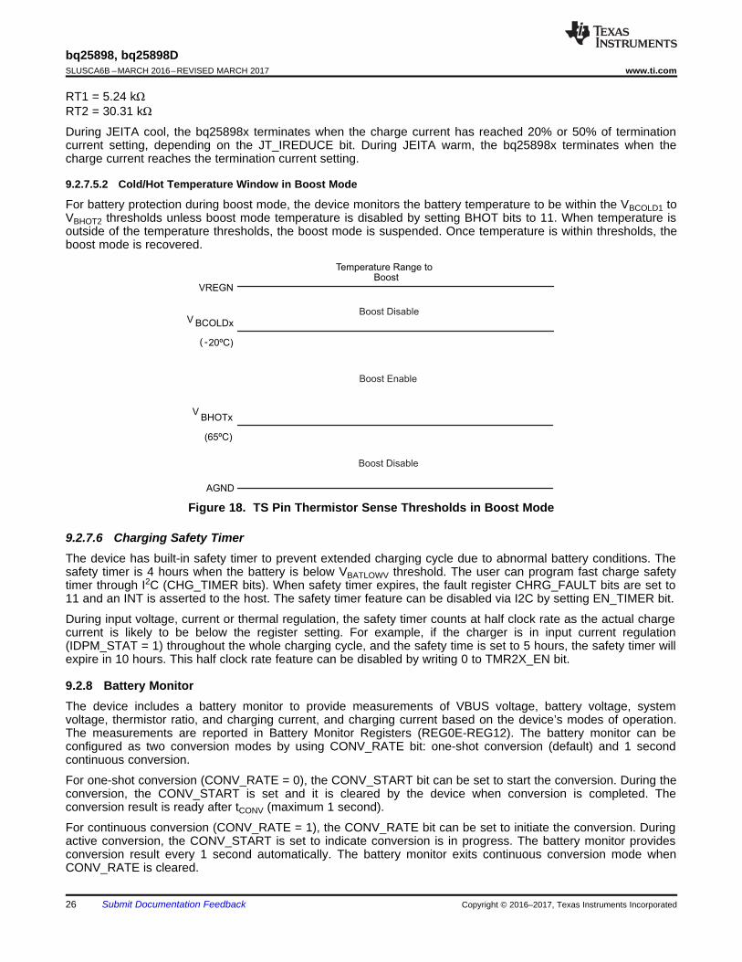
9.2.7.5.2 Cold/Hot Temperature Window in Boost Mode
For battery protection during boost mode, the device monitors the battery temperature to be within the VBCOLD1 toVBHOT2 thresholds unless boost mode temperature is disabled by setting BHOT bits to 11. When temperature isoutside of the temperature thresholds, the boost mode is suspended. Once temperature is within thresholds, theboost mode is recovered.
Figure 18. TS Pin Thermistor Sense Thresholds in Boost Mode
9.2.7.6 Charging Safety TimerThe device has built-in safety timer to prevent extended charging cycle due to abnormal battery conditions. Thesafety timer is 4 hours when the battery is below VBATLOWV threshold. The user can program fast charge safetytimer through I2C (CHG_TIMER bits). When safety timer expires, the fault register CHRG_FAULT bits are set to11 and an INT is asserted to the host. The safety timer feature can be disabled via I2C by setting EN_TIMER bit.
During input voltage, current or thermal regulation, the safety timer counts at half clock rate as the actual chargecurrent is likely to be below the register setting. For example, if the charger is in input current regulation(IDPM_STAT = 1) throughout the whole charging cycle, and the safety time is set to 5 hours, the safety timer willexpire in 10 hours. This half clock rate feature can be disabled by writing 0 to TMR2X_EN bit.
9.2.8 Battery MonitorThe device includes a battery monitor to provide measurements of VBUS voltage, battery voltage, systemvoltage, thermistor ratio, and charging current, and charging current based on the device’s modes of operation.The measurements are reported in Battery Monitor Registers (REG0E-REG12). The battery monitor can beconfigured as two conversion modes by using CONV_RATE bit: one-shot conversion (default) and 1 secondcontinuous conversion.
For one-shot conversion (CONV_RATE = 0), the CONV_START bit can be set to start the conversion. During theconversion, the CONV_START is set and it is cleared by the device when conversion is completed. Theconversion result is ready after tCONV (maximum 1 second).
For continuous conversion (CONV_RATE = 1), the CONV_RATE bit can be set to initiate the conversion. Duringactive conversion, the CONV_START is set to indicate conversion is in progress. The battery monitor providesconversion result every 1 second automatically. The battery monitor exits continuous conversion mode whenCONV_RATE is cleared.
When battery monitor is active, the REGN power is enabled and can increase device quiescent current.
Table 7. Battery Monitor Modes of Operation
PARAMETER REGISTERMODES OF OPERATION
CHARGEMODE BOOST MODE DISABLE CHARGE
MODEBATTERY ONLY
MODEBattery Voltage (VBAT) REG0E Yes Yes Yes YesSystem Voltage (VSYS) REG0F Yes Yes Yes Yes
Temperature (TS) Voltage (VTS) REG10 Yes Yes Yes YesVBUS Voltage (VVBUS) REG11 Yes Yes Yes NACharge Current (IBAT) REG12 Yes NA NA NA
9.2.9 Status Outputs (PG, STAT, and INT)
9.2.9.1 Power Good Indicator (PG)In bq25898, the PG goes LOW to indicate a good input source when:1. VBUS above VVBUS_UVLO
2. VBUS above battery (not in sleep)3. VBUS below VACOV threshold4. VBUS above VVBUSMIN (typical 3.8 V) when IBADSRC (typical 30 mA) current is applied (not a poor source)5. Completed Input Source Type Detection
9.2.9.2 Charging Status Indicator (STAT)The device indicates charging state on the open drain STAT pin. The STAT pin can drive LED as shown inFigure 49. The STAT pin function can be disable by setting STAT_DIS bit.
Table 8. STAT Pin StateCHARGING STATE STAT INDICATOR
Charging in progress (including recharge) LOWCharging complete HIGHSleep mode, charge disable HIGHCharge suspend (Input overvoltage, TS fault, timer fault, input or system overvoltage)Boost Mode suspend (due to TS Fault) blinking at 1 Hz
9.2.9.3 Interrupt to Host (INT)In some applications, the host does not always monitor the charger operation. The INT notifies the system on thedevice operation. The following events will generate 256-µs INT pulse.• USB/adapter source identified (through PSEL or DPDM detection, with OTG pin)• Good input source detected
– VBUS above battery (not in sleep)– VBUS below VACOV threshold– VBUS above VVBUSMIN (typical 3.8 V) when IBADSRC (typical 30 mA) current is applied (not a poor source)
• Input removed• Charge Complete• Any FAULT event in REG0C
When a fault occurs, the charger device sends out INT and keeps the fault state in REG0C until the host readsthe fault register. Before the host reads REG0C and all the faults are cleared, the charger device would not sendany INT upon new faults. To read the current fault status, the host has to read REG0C two times consecutively.The 1st read reports the pre-existing fault register status and the 2nd read reports the current fault register status.
9.2.10.1 BATFET Disable Mode (Shipping Mode)To extend battery life and minimize power when system is powered off during system idle, shipping, or storage,the device can turn off BATFET so that the system voltage is zero to minimize the battery leakage current. Whenthe host set BATFET_DIS bit, the charger can turn off BATFET immediately or delay by tSM_DLY as configuratedby BATFET_DLY bit.
9.2.10.2 BATFET Enable (Exit Shipping Mode)When the BATFET is disabled (in shipping mode) and indicated by setting BATFET_DIS, one of the followingevents can enable BATFET to restore system power:1. Plug in adapter2. Clear BATFET_DIS bit3. Set REG_RST bit to reset all registers including BATFET_DIS bit to default (0)4. A logic high to low transition on QON pin with tSHIPMODE deglitch time to enable BATFET to exit shipping
mode
9.2.10.3 BATFET Full System ResetThe BATFET functions as a load switch between battery and system when input source is not plugged-in. Bychanging the state of BATFET from off to on, system connects to SYS can be effectively have a power-on-reset.The QON pin supports push-button interface to reset system power without host by change the state of BATFET.
When the QON pin is driven to logic low for tQON_RST (typical 15 seconds) while input source is not plugged inand BATFET is enabled (BATFET_DIS=0), the BATFET is turned off for tBATFET_RST and then it is re-enabled toreset system power. This function can be disabled by setting BATFET_RST_EN bit to 0.
9.2.11 Current Pulse Control ProtocolThe device provides the control to generate the VBUS current pulse protocol to communicate with adjustablehigh voltage adapter in order to signal adapter to increase or decrease output voltage. To enable the interface,the EN_PUMPX bit must be set. Then the host can select the increase/decrease voltage pulse by setting one ofthe PUMPX_UP or PUMPX_DN bit (but not both) to start the VBUS current pulse sequence. During the currentpulse sequence, the PUMPX_UP and PUMPX_DN bits are set to indicate pulse sequence is in progress and thedevice pulses the input current limit between current limit set forth by IINLIM or IDPM_LIM register and the100mA current limit (IINDPM100_ACC). When the pulse sequence is completed, the input current limit is returned tovalue set by IINLIM or IDPM_LIM register and the PUMPX_UP or PUMPX_DN bit is cleared. In addition, theEN_PUMPX can be cleared during the current pulse sequence to terminate the sequence and force charger toreturn to input current limit as set forth by the IINLIM or IDPM_LIM register immediately. When EN_PUMPX bit islow, write to PUMPX_UP and PUMPX_DN bit would be ignored and have no effect on VBUS current limit.
9.2.12 Input Current Limit on ILIMFor safe operation, the device has an additional hardware pin on ILIM to limit maximum input current on ILIM pin.The input maximum current is set by a resistor from ILIM pin to ground as:
(3)
The actual input current limit is the lower value between ILIM setting and register setting (IINLIM). For example, ifthe register setting is 111111 for 3.25 A, and ILIM has a 232-Ω resistor (KILIM = 350 max.) to ground for 1.5 A,the input current limit is 1.5 A. ILIM pin can be used to set the input current limit rather than the register settingswhen EN_ILIM bit is set. The device regulates ILIM pin at 0.8 V. If ILIM voltage exceeds 0.8 V, the device entersinput current regulation (Refer to Dynamic Power Management section).
The ILIM pin can also be used to monitor input current when EN_ILIM is enabled. The voltage on ILIM pin isproportional to the input current. ILIM pin can be used to monitor the input current following Equation 4:
For example, if ILIM pin is set with 260-Ω resistor, and the ILIM voltage is 0.4 V, the actual input current 0.557 A- 0.67 A (based on KILM specified). If ILIM pin is open, the input current is limited to zero since ILIM voltagefloats above 0.8 V. If ILIM pin is short, the input current limit is set by the register.
The ILIM pin function can be disabled by setting EN_ILIM bit to 0. When the pin is disabled, both input currentlimit function and monitoring function are not available.
9.2.13 Thermal Regulation and Thermal Shutdown
9.2.13.1 Thermal Protection in Buck ModeThe device monitors the internal junction temperature TJ to avoid overheat the chip and limits the IC surfacetemperature in buck mode. When the internal junction temperature exceeds the preset thermal regulation limit(TREG bits), the device lowers down the charge current. The wide thermal regulation range from 60ºC to 120ºCallows the user to optimize the system thermal performance.
During thermal regulation, the actual charging current is usually below the programmed battery charging current.Therefore, termination is disabled, the safety timer runs at half the clock rate, and the status registerTHERM_STAT bit goes high.
Additionally, the device has thermal shutdown to turn off the converter and BATFET when IC surfacetemperature exceeds TSHUT. The fault register CHRG_FAULT is set to 10 and an INT is asserted to the host. TheBATFET and converter is enabled to recover when IC temperature is below TSHUT_HYS.
9.2.13.1.1 Thermal Protection in Boost Mode
The device monitors the internal junction temperature to provide thermal shutdown during boost mode. When ICsurface temperature exceeds TSHUT, the boost mode is disabled (converter is turned off) by settingOTG_CONFIG bit low and BATFET is turned off. When IC surface temperature is below TSHUT_HYS, the BATFETis enabled automatically to allow system to restore and the host can re-enable OTG_CONFIG bit to recover.
9.2.14 Voltage and Current Monitoring in Buck and Boost Mode
9.2.14.1 Voltage and Current Monitoring in Buck ModeThe device closely monitors the input and system voltage, as well as HSFET current for safe buck and boostmode operations.
9.2.14.1.1 Input Overvoltage (ACOV)
The input voltage for buck mode operation is VVBUS_OP. If VBUS voltage exceeds VACOV, the device stopsswitching immediately. During input over voltage (ACOV), the fault register CHRG_FAULT bits sets to 01. An INTis asserted to the host.
9.2.14.1.2 System Overvoltage Protection (SYSOVP)
The charger device clamps the system voltage during load transient so that the components connect to systemwould not be damaged due to high voltage. When SYSOVP is detected, the converter stops immediately toclamp the overshoot.
9.2.14.2 Voltage and Current Monitoring in Boost ModeThe device closely monitors the VBUS voltage, as well as RBFET and LSFET current to ensure safe boost modeoperation.
9.2.14.2.1 VBUS Overcurrent Protection
The charger device closely monitors the RBFET (Q1), and LSFET (Q3) current to ensure safe boost modeoperation. During overcurrent condition when output current exceed (IOTG_OCP) the device operates in hiccupmode for protection. While in hiccup mode cycle, the device turns off RBFET for tOTG_OCP_OFF (30 ms typical) andturns on RBFET for tOTG_OCP_ON (250 µs typical) in an attempt to restart. If the overcurrent condition is removed,the boost converter returns to normal operation. When overcurrent condition continues to exist, the devicerepeats the hiccup cycle until overcurrent condition is removed. When overcurrent condition is detected the faultregister bit BOOST_FAULT is set high to indicate fault in boost operation. An INT is also asserted to the host.
When the VBUS voltage rises above regulation target and exceeds VOTG_OVP, the device enters overvoltageprotection which stops switching, clears OTG_CONFIG bit and exits boost mode. During the overvoltageduration, the fault register bit (BOOST_FAULT) is set high to indicate fault in boost operation. An INT is alsoasserted to the host.
9.2.15 Battery Protection
9.2.15.1 Battery Overvoltage Protection (BATOVP)The battery overvoltage limit is clamped at 4% above the battery regulation voltage. When battery over voltageoccurs, the charger device immediately disables charge. The fault register BAT_FAULT bit goes high and an INTis asserted to the host.
9.2.15.2 Battery Over-Discharge ProtectionWhen battery is discharged below VBAT_DPL, the BATFET is turned off to protect battery from over discharge. Torecover from over-discharge, an input source is required at VBUS. When an input source is plugged in, theBATFET turns on. Thy is charged with IBATSHORT (typically 100 mA) current when the VBAT < VSHORT, orprecharge current as set in IPRECHG register when the battery voltage is between VSHORT and VBATLOWV.
9.2.15.3 System Overcurrent ProtectionWhen the system is shorted or significantly overloaded (IBAT > IBATOP) so that its current exceeds the overcurrentlimit, the device latches off BATFET. Section BATFET Enable (Exit Shipping Mode) can reset the latch-offcondition and turn on BATFET.
9.2.16 Serial InterfaceThe device uses I2C compatible interface for flexible charging parameter programming and instantaneous devicestatus reporting. I2C is a bi-directional 2-wire serial interface. Only two open-drain bus lines are required: a serialdata line (SDA) and a serial clock line (SCL). Devices can be considered as masters or slaves when performingdata transfers. A master is the device which initiates a data transfer on the bus and generates the clock signalsto permit that transfer. At that time, any device addressed is considered a slave.
The device operates as a slave device with address 6BH, receiving control inputs from the master device likemicro controller or a digital signal processor through REG00-REG14. Register read beyond REG14 (0x14)returns 0xFF. The I2C interface supports both standard mode (up to 100 kbits), and fast mode (up to 400 kbits).When the bus is free, both lines are HIGH. The SDA and SCL pins are open drain and must be connected to thepositive supply voltage via a current source or pull-up resistor.
9.2.16.1 Data ValidityThe data on the SDA line must be stable during the HIGH period of the clock. The HIGH or LOW state of thedata line can only change when the clock signal on the SCL line is LOW. One clock pulse is generated for eachdata bit transferred.
9.2.16.2 START and STOP ConditionsAll transactions begin with a START (S) and can be terminated by a STOP (P). A HIGH to LOW transition on theSDA line while SCl is HIGH defines a START condition. A LOW to HIGH transition on the SDA line when theSCL is HIGH defines a STOP condition.
START and STOP conditions are always generated by the master. The bus is considered busy after the STARTcondition, and free after the STOP condition.
Figure 20. START and STOP conditions
9.2.16.3 Byte FormatEvery byte on the SDA line must be 8 bits long. The number of bytes to be transmitted per transfer isunrestricted. Each byte has to be followed by an Acknowledge bit. Data is transferred with the Most SignificantBit (MSB) first. If a slave cannot receive or transmit another complete byte of data until it has performed someother function, it can hold the clock line SCL low to force the master into a wait state (clock stretching). Datatransfer then continues when the slave is ready for another byte of data and release the clock line SCL.
Figure 21. Data Transfer on the I2C Bus
9.2.16.4 Acknowledge (ACK) and Not Acknowledge (NACK)The acknowledge takes place after every byte. The acknowledge bit allows the receiver to signal the transmitterthat the byte was successfully received and another byte may be sent. All clock pulses, including theacknowledge 9th clock pulse, are generated by the master.
The transmitter releases the SDA line during the acknowledge clock pulse so the receiver can pull the SDA lineLOW and it remains stable LOW during the HIGH period of this clock pulse.
When SDA remains HIGH during the 9th clock pulse, this is the Not Acknowledge signal. The master can thengenerate either a STOP to abort the transfer or a repeated START to start a new transfer.
9.2.16.5 Slave Address and Data Direction BitAfter the START, a slave address is sent. This address is 7 bits long followed by the eighth bit as a data directionbit (bit R/W). A zero indicates a transmission (WRITE) and a one indicates a request for data (READ).
REG0C is a fault register. It keeps all the fault information from last read until the host issues a new read. Forexample, if Charge Safety Timer Expiration fault occurs but recovers later, the fault register REG0C reports thefault when it is read the first time, but returns to normal when it is read the second time. In order to get the faultinformation at present, the host has to read REG0C for the second time. The only exception is NTC_FAULTwhich always reports the actual condition on the TS pin. In addition, REG0C does not support multi-read andmulti-write.
9.3 Device Functional Modes
9.3.1 Host Mode and Default ModeThe device is a host controlled charger, but it can operate in default mode without host management. In defaultmode, the device can be used an autonomous charger with no host or while host is in sleep mode. When thecharger is in default mode, WATCHDOG_FAULT bit is HIGH. When the charger is in host mode,WATCHDOG_FAULT bit is LOW.
After power-on-reset, the device starts in default mode with watchdog timer expired, or default mode. All theregisters are in the default settings.
In default mode, the device keeps charging the battery with 12-hour fast charging safety timer. At the end of the12-hour, the charging is stopped and the buck converter continues to operate to supply system load. Any writecommand to device transitions the charger from default mode to host mode. All the device parameters can beprogrammed by the host. To keep the device in host mode, the host has to reset the watchdog timer by writing 1to WD_RST bit before the watchdog timer expires (WATCHDOG_FAULT bit is set), or disable watchdog timer bysetting WATCHDOG bits=00.
When the watchdog timer (WATCHDOG_FAULT bit = 1) is expired, the device returns to default mode and allregisters are reset to default values except IINLIM, VINDPM, VINDPM_OS, BATFET_RST_EN, BATFET_DLY,and BATFET_DIS bits.
R/W R/W R/W R/W R/W R/W R/W R/WLEGEND: R/W = Read/Write; R = Read only; -n = value after reset
Table 11. REG02Bit Field Type Reset Description
7 CONV_START R/W by REG_RSTby Watchdog
ADC Conversion Start Control0 – ADC conversion not active (default).1 – Start ADC ConversionThis bit is read-only when CONV_RATE = 1. The bit stays high duringADC conversion and during input source detection.
Force D+/D- Detection0 – Not in D+/D- or PSEL detection (default)1 – Force D+/D- detection
0 AUTO_DPDM_EN R/W by REG_RSTAutomatic D+/D- Detection Enable0 –Disable D+/D- or PSEL detection when VBUS is plugged-in1 –Enable D+/D- or PEL detection when VBUS is plugged-in (default)
R/W R/W R/W R/W R/W R/W R/W R/WLEGEND: R/W = Read/Write; R = Read only; -n = value after reset
Table 18. REG09Bit Field Type Reset Description
7 FORCE_ICO R/W by REG_RSTby Watchdog
Force Start Input Current Optimizer (ICO)0 – Do not force ICO (default)1 – Force ICONote:This bit is can only be set only and always returns to 0 after ICO starts
6 TMR2X_EN R/W by REG_RSTby Watchdog
Safety Timer Setting during DPM or Thermal Regulation0 – Safety timer not slowed by 2X during input DPM or thermalregulation1 – Safety timer slowed by 2X during input DPM or thermal regulation(default)
5 BATFET_DIS R/W by REG_RSTForce BATFET off to enable ship mode with tSM_DLY delay time0 – Allow BATFET turn on (default)1 – Force BATFET off
4 JEITA_VSET (45C-60C) R/W by REG_RSTby Watchdog
JEITA High Temperature Voltage Setting0 – Set Charge Voltage to VREG-200mV during JEITA hig temperature(default)1 – Set Charge Voltage to VREG during JEITA high temperature
3 BATFET_DLY R/W by REG_RSTBATFET turn off delay control0 – BATFET turn off immediately when BATFET_DIS bit is set (default)1 – BATFET turn off delay by tSM_DLY when BATFET_DIS bit is set
2 BATFET_RST_EN R/W by REG_RSTBATFET full system reset enable0 – Disable BATFET full system reset1 – Enable BATFET full system reset (default)
1 PUMPX_UP R/W by REG_RSTby Watchdog
Current pulse control voltage up enable0 – Disable (default)1 – EnableNote:This bit is can only be set when EN_PUMPX bit is set and returns to 0after current pulse control sequence is completed
0 PUMPX_DN R/W by REG_RSTby Watchdog
Current pulse control voltage down enable0 – Disable (default)1 – EnableNote:This bit is can only be set when EN_PUMPX bit is set and returns to 0after current pulse control sequence is completed
LEGEND: R/W = Read/Write; R = Read only; -n = value after reset
Table 20. REG0BBit Field Type Reset Description
7 VBUS_STAT[2] R N/A VBUS Status registerbq25898D000: No Input 001: USB Host SDP010: USB CDP (1.5A)011: USB DCP (3.25A)100: Adjustable High Voltage DCP (MaxCharge) (1.5A)101: Unknown Adapter (500mA)110: Non-Standard Adapter (1A/2A/2.1A/2.4A)111: OTGbq25898000: No Input001: USB Host SDP010: Adapter (3.25A)111: OTGNote: Software current limit is reported in IINLIM register
6 VBUS_STAT[1] R N/A
5 VBUS_STAT[0] R N/A
4 CHRG_STAT[1] R N/A Charging Status00 – Not Charging01 – Pre-charge ( < VBATLOWV)10 – Fast Charging11 – Charge Termination Done
3 CHRG_STAT[0] R N/A
2 PG_STAT R N/APower Good Status0 – Not Power Good1 – Power Good
1 Reserved R N/A Reserved: Always reads 1
0 VSYS_STAT R N/AVSYS Regulation Status0 – Not in VSYSMIN regulation (BAT > VSYSMIN)1 – In VSYSMIN regulation (BAT < VSYSMIN)
R/W R/W R/W R/W R/W R/W R/W R/WLEGEND: R/W = Read/Write; R = Read only; -n = value after reset
Table 22. REG0DBit Field Type Reset Description
7 FORCE_VINDPM R/W by REG_RSTVINDPM Threshold Setting Method0 – Run Relative VINDPM Threshold (default)1 – Run Absolute VINDPM Threshold
6 VINDPM[6] R/W by REG_RST 6400mV Absolute VINDPM ThresholdOffset: 2.6VRange: 3.9V (0001101) – 15.3V (1111111)Default: 4.4V (0010010)Note:Value < 0001101 is clamped to 3.9V (0001101)Register is read only when FORCE_VINDPM=0 and canbe written by internal control based on relative VINDPMthreshold settingRegister can be read/write when FORCE_VINDPM = 1
5 VINDPM[5] R/W by REG_RST 3200mV
4 VINDPM[4] R/W by REG_RST 1600mV
3 VINDPM[3] R/W by REG_RST 800mV
2 VINDPM[2] R/W by REG_RST 400mV
1 VINDPM[1] R/W by REG_RST 200mV
0 VINDPM[0] R/W by REG_RST 100mV
9.4.15 REG0E
Figure 42. REG0E
7 6 5 4 3 2 1 00 0 0 0 0 0 0 0R R R R R R R R
LEGEND: R/W = Read/Write; R = Read only; -n = value after reset
Table 23. REG0EBit Field Type Reset Description
7 THERM_STAT R N/AThermal Regulation Status0 – Normal1 – In Thermal Regulation
6 BATV[6] R N/A 1280mV
ADC conversion of Battery Voltage (VBAT)Offset: 2.304VRange: 2.304V (0000000) – 4.848V (1111111)Default: 2.304V (0000000)
LEGEND: R/W = Read/Write; R = Read only; -n = value after reset
Table 28. REG13Bit Field Type Reset Description
7 VDPM_STAT R N/AVINDPM Status0 – Not in VINDPM1 – VINDPM
6 IDPM_STAT R N/AIINDPM Status0 – Not in IINDPM1 – IINDPM
5 IDPM_LIM[5] R N/A 1600mA
Input Current Limit in effect while Input Current Optimizer(ICO) is enabledOffset: 100mA (default)Range 100mA (0000000) – 3.25mA (1111111)
4 IDPM_LIM[4] R N/A 800mA
3 IDPM_LIM[3] R N/A 400mA
2 IDPM_LIM[2] R N/A 200mA
1 IDPM_LIM[1] R N/A 100mA
0 IDPM_LIM[0] R N/A 50mA
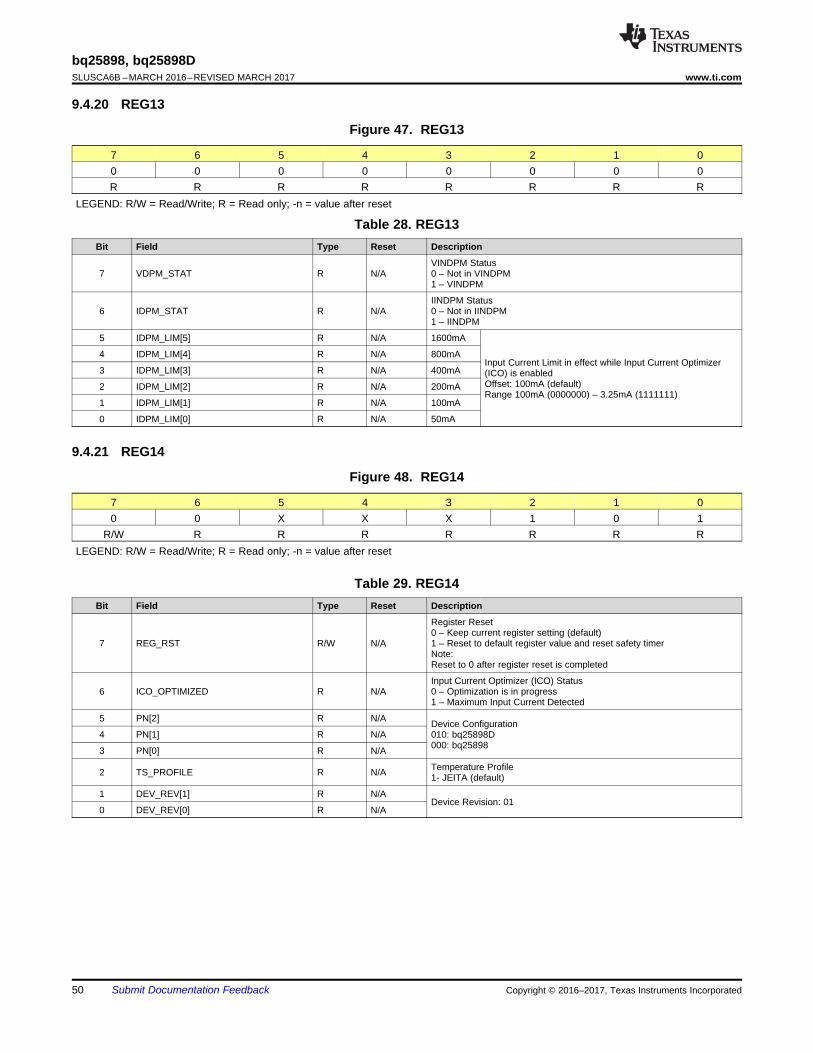
9.4.21 REG14
Figure 48. REG14
7 6 5 4 3 2 1 00 0 X X X 1 0 1
R/W R R R R R R RLEGEND: R/W = Read/Write; R = Read only; -n = value after reset
Table 29. REG14Bit Field Type Reset Description
7 REG_RST R/W N/A
Register Reset0 – Keep current register setting (default)1 – Reset to default register value and reset safety timerNote:Reset to 0 after register reset is completed
6 ICO_OPTIMIZED R N/AInput Current Optimizer (ICO) Status0 – Optimization is in progress1 – Maximum Input Current Detected
5 PN[2] R N/A Device Configuration010: bq25898D000: bq25898
4 PN[1] R N/A
3 PN[0] R N/A
2 TS_PROFILE R N/A Temperature Profile1- JEITA (default)
NOTEInformation in the following applications sections is not part of the TI componentspecification, and TI does not warrant its accuracy or completeness. TI’s customers areresponsible for determining suitability of components for their purposes. Customers shouldvalidate and test their design implementation to confirm system functionality.
10.1 Application InformationA typical application consists of the device configured as an I2C controlled power path management device and asingle cell battery charger for Li-Ion and Li-polymer batteries used in a wide range of smartphones and otherportable devices. It integrates an input reverse-block FET (RBFET, Q1), high-side switching FET (HSFET, Q2),low-side switching FET (LSFET, Q3), and BATFET (Q4) between the system and battery. The device alsointegrates a bootstrap diode for the high-side gate drive.
10.2 Typical Application Diagram
VREF is the pull up voltage of I2C communication interface
Figure 49. bq25898D Application Diagram with PSEL with Interface and USB On-The-Go (OTG)
10.2.1 Design RequirementsFor this design example, use the parameters shown in Table 30.
Table 30. Design ParametersPARAMETER VALUE
Input voltage range 3.9 V to 14 VInput current limit 1.5 A
10.2.2.1 Inductor SelectionThe device has 1.5 MHz switching frequency to allow the use of small inductor and capacitor values. TheInductor saturation current should be higher than the charging current (ICHG) plus half the ripple current (IRIPPLE):
(5)
The inductor ripple current depends on input voltage (VBUS), duty cycle (D = VBAT/VVBUS), switching frequency (fs)and inductance (L):
(6)
The maximum inductor ripple current happens with D = 0.5 or close to 0.5. Usually inductor ripple is designed inthe range of (20–40%) maximum charging current as a trade-off between inductor size and efficiency for apractical design.
10.2.2.2 Buck Input Capacitor
Input capacitor should have enough ripple current rating to absorb input switching ripple current. The worst caseRMS ripple current is half of the charging current when duty cycle is 0.5. If the converter does not operate at50% duty cycle, then the worst case capacitor RMS current IPMID occurs where the duty cycle is closest to 50%and can be estimated by Equation 7:
(7)
Low ESR ceramic capacitor such as X7R or X5R is preferred for input decoupling capacitor and should beplaced to the drain of the high side MOSFET and source of the low side MOSFET as close as possible. Voltagerating of the capacitor must be higher than normal input voltage level. 25 V rating or higher capacitor is preferredfor up to 14-V input voltage. 8.2-μF capacitance is suggested for typical of 3 A – 5 A charging current.
10.2.2.3 System Output Capacitor
Output capacitor also should have enough ripple current rating to absorb output switching ripple current. Theoutput capacitor RMS current ICOUT is given:
(8)
The output capacitor voltage ripple can be calculated as follows:
(9)
At certain input/output voltage and switching frequency, the voltage ripple can be reduced by increasing theoutput filter LC. The charger device has internal loop compensator. To get good loop stability, 1-µH and minimumof 20-µF output capacitor is recommended. The preferred ceramic capacitor is 6V or higher rating, X7R or X5R.
11 Power Supply RecommendationsIn order to provide an output voltage on SYS, the device requires a power supply between 3.9 V and 14 V inputwith at least 100-mA current rating connected to VBUS or a single-cell Li-Ion battery with voltage > VBATUVLOconnected to BAT. The source current rating needs to be at least 3 A in order for the buck converter of thecharger to provide maximum output power to SYS.
12 Layout
12.1 Layout GuidelinesThe switching node rise and fall times should be minimized for minimum switching loss. Proper layout of thecomponents to minimize high frequency current path loop (see Figure 66) is important to prevent electrical andmagnetic field radiation and high frequency resonant problems. Here is a PCB layout priority list for properlayout. Layout PCB according to this specific order is essential.1. Place input capacitor as close as possible to PMID pin and GND pin connections and use shortest copper
trace connection or GND plane.2. Put output capacitor near to the inductor and the IC.3. Decoupling capacitors should be placed next to the IC pins and make trace connection as short as possible.4. Place inductor input terminal to SW pin as close as possible. Minimize the copper area of this trace to lower
electrical and magnetic field radiation but make the trace wide enough to carry the charging current. Do notuse multiple layers in parallel for this connection. Minimize parasitic capacitance from this area to any othertrace or plane.
5. Connect all grounds together to reduce PCB size and improve thermal dissipation.6. Avoid ground planes in parallel with high frequency traces in other layers.
13.1.1 Third-Party Products DisclaimerTI'S PUBLICATION OF INFORMATION REGARDING THIRD-PARTY PRODUCTS OR SERVICES DOES NOTCONSTITUTE AN ENDORSEMENT REGARDING THE SUITABILITY OF SUCH PRODUCTS OR SERVICESOR A WARRANTY, REPRESENTATION OR ENDORSEMENT OF SUCH PRODUCTS OR SERVICES, EITHERALONE OR IN COMBINATION WITH ANY TI PRODUCT OR SERVICE.
13.2 Related LinksThe table below lists quick access links. Categories include technical documents, support and communityresources, tools and software, and quick access to sample or buy.
Table 31. Related Links
PARTS PRODUCT FOLDER ORDER NOW TECHNICALDOCUMENTS
TOOLS &SOFTWARE
SUPPORT &COMMUNITY
bq25898 Click here Click here Click here Click here Click herebq25898D Click here Click here Click here Click here Click here
13.3 Receiving Notification of Documentation UpdatesTo receive notification of documentation updates, navigate to the device product folder on ti.com. In the upperright corner, click on Alert me to register and receive a weekly digest of any product information that haschanged. For change details, review the revision history included in any revised document.
13.4 Community ResourcesThe following links connect to TI community resources. Linked contents are provided "AS IS" by the respectivecontributors. They do not constitute TI specifications and do not necessarily reflect TI's views; see TI's Terms ofUse.
TI E2E™ Online Community TI's Engineer-to-Engineer (E2E) Community. Created to foster collaborationamong engineers. At e2e.ti.com, you can ask questions, share knowledge, explore ideas and helpsolve problems with fellow engineers.
Design Support TI's Design Support Quickly find helpful E2E forums along with design support tools andcontact information for technical support.
13.5 TrademarksMaxCharge, E2E are trademarks of Texas Instruments.All other trademarks are the property of their respective owners.
13.6 Electrostatic Discharge CautionThese devices have limited built-in ESD protection. The leads should be shorted together or the device placed in conductive foamduring storage or handling to prevent electrostatic damage to the MOS gates.
13.7 GlossarySLYZ022 — TI Glossary.
This glossary lists and explains terms, acronyms, and definitions.
14 Mechanical, Packaging, and Orderable InformationThe following pages include mechanical, packaging, and orderable information. This information is the mostcurrent data available for the designated devices. This data is subject to change without notice and revision ofthis document. For browser-based versions of this data sheet, refer to the left-hand navigation.
DSBGA - 0.625 mm max heightYFF0042DIE SIZE BALL GRID ARRAY
NOTES: 1. All linear dimensions are in millimeters. Any dimensions in parenthesis are for reference only. Dimensioning and tolerancing per ASME Y14.5M. 2. This drawing is subject to change without notice.
BUMP A1CORNER
SEATING PLANE
BALL TYP 0.05 C
A
B
C
D
1 2 3
0.015 C A B
E
54
F
G
SYMM
SYMM
6
SCALE 4.500
D: Max =
E: Max =
2.85mm, Min = 2.79mm
2.56mm, Min = 2.50mm
www.ti.com
EXAMPLE BOARD LAYOUT
42X ( )0.23 (0.4) TYP
(0.4) TYP
( )METAL
0.23 0.05 MAX
SOLDER MASKOPENING
METAL UNDERSOLDER MASK
( )SOLDER MASKOPENING
0.230.05 MIN
4222067/A 05/2015
DSBGA - 0.625 mm max heightYFF0042DIE SIZE BALL GRID ARRAY
NOTES: (continued) 3. Final dimensions may vary due to manufacturing tolerance considerations and also routing constraints. For more information, see Texas Instruments literature number SNVA009 (www.ti.com/lit/snva009).
SOLDER MASK DETAILSNOT TO SCALE
SYMM
SYMM
LAND PATTERN EXAMPLESCALE:25X
A
B
C
D
1 2 3 4 5
E
F
G
6
NON-SOLDER MASKDEFINED
(PREFERRED)
SOLDER MASKDEFINED
www.ti.com
EXAMPLE STENCIL DESIGN
(0.4)TYP
(0.4) TYP
42X ( 0.25) (R ) TYP0.05
METALTYP
4222067/A 05/2015
DSBGA - 0.625 mm max heightYFF0042DIE SIZE BALL GRID ARRAY
NOTES: (continued) 4. Laser cutting apertures with trapezoidal walls and rounded corners may offer better paste release.
6
SYMM
SYMM
SOLDER PASTE EXAMPLEBASED ON 0.1 mm THICK STENCIL
SCALE:30X
A
B
C
D
1 2 3
E
4 5
F
G
PACKAGE OPTION ADDENDUM
www.ti.com 17-Mar-2017
Addendum-Page 1
PACKAGING INFORMATION
Orderable Device Status(1)
Package Type PackageDrawing
Pins PackageQty
Eco Plan(2)
Lead/Ball Finish(6)
MSL Peak Temp(3)
Op Temp (°C) Device Marking(4/5)
Samples
BQ25898DYFFR ACTIVE DSBGA YFF 42 3000 Green (RoHS& no Sb/Br)
SNAGCU Level-1-260C-UNLIM -40 to 125 BQ25898D
BQ25898DYFFT ACTIVE DSBGA YFF 42 250 Green (RoHS& no Sb/Br)
SNAGCU Level-1-260C-UNLIM -40 to 125 BQ25898D
BQ25898YFFR ACTIVE DSBGA YFF 42 3000 Green (RoHS& no Sb/Br)
SNAGCU Level-1-260C-UNLIM -40 to 125 BQ25898
BQ25898YFFT ACTIVE DSBGA YFF 42 250 Green (RoHS& no Sb/Br)
SNAGCU Level-1-260C-UNLIM -40 to 125 BQ25898
(1) The marketing status values are defined as follows:ACTIVE: Product device recommended for new designs.LIFEBUY: TI has announced that the device will be discontinued, and a lifetime-buy period is in effect.NRND: Not recommended for new designs. Device is in production to support existing customers, but TI does not recommend using this part in a new design.PREVIEW: Device has been announced but is not in production. Samples may or may not be available.OBSOLETE: TI has discontinued the production of the device.
(2) Eco Plan - The planned eco-friendly classification: Pb-Free (RoHS), Pb-Free (RoHS Exempt), or Green (RoHS & no Sb/Br) - please check http://www.ti.com/productcontent for the latest availabilityinformation and additional product content details.TBD: The Pb-Free/Green conversion plan has not been defined.Pb-Free (RoHS): TI's terms "Lead-Free" or "Pb-Free" mean semiconductor products that are compatible with the current RoHS requirements for all 6 substances, including the requirement thatlead not exceed 0.1% by weight in homogeneous materials. Where designed to be soldered at high temperatures, TI Pb-Free products are suitable for use in specified lead-free processes.Pb-Free (RoHS Exempt): This component has a RoHS exemption for either 1) lead-based flip-chip solder bumps used between the die and package, or 2) lead-based die adhesive used betweenthe die and leadframe. The component is otherwise considered Pb-Free (RoHS compatible) as defined above.Green (RoHS & no Sb/Br): TI defines "Green" to mean Pb-Free (RoHS compatible), and free of Bromine (Br) and Antimony (Sb) based flame retardants (Br or Sb do not exceed 0.1% by weightin homogeneous material)
(3) MSL, Peak Temp. - The Moisture Sensitivity Level rating according to the JEDEC industry standard classifications, and peak solder temperature.
(4) There may be additional marking, which relates to the logo, the lot trace code information, or the environmental category on the device.
(5) Multiple Device Markings will be inside parentheses. Only one Device Marking contained in parentheses and separated by a "~" will appear on a device. If a line is indented then it is a continuationof the previous line and the two combined represent the entire Device Marking for that device.
(6) Lead/Ball Finish - Orderable Devices may have multiple material finish options. Finish options are separated by a vertical ruled line. Lead/Ball Finish values may wrap to two lines if the finishvalue exceeds the maximum column width.
Important Information and Disclaimer:The information provided on this page represents TI's knowledge and belief as of the date that it is provided. TI bases its knowledge and belief on informationprovided by third parties, and makes no representation or warranty as to the accuracy of such information. Efforts are underway to better integrate information from third parties. TI has taken andcontinues to take reasonable steps to provide representative and accurate information but may not have conducted destructive testing or chemical analysis on incoming materials and chemicals.TI and TI suppliers consider certain information to be proprietary, and thus CAS numbers and other limited information may not be available for release.
In no event shall TI's liability arising out of such information exceed the total purchase price of the TI part(s) at issue in this document sold by TI to Customer on an annual basis.
DSBGA - 0.625 mm max heightYFF0042DIE SIZE BALL GRID ARRAY
NOTES: 1. All linear dimensions are in millimeters. Any dimensions in parenthesis are for reference only. Dimensioning and tolerancing per ASME Y14.5M. 2. This drawing is subject to change without notice.
BUMP A1CORNER
SEATING PLANE
BALL TYP 0.05 C
A
B
C
D
1 2 3
0.015 C A B
E
54
F
G
SYMM
SYMM
6
SCALE 4.500
D: Max =
E: Max =
2.852 mm, Min =
2.558 mm, Min =
2.792 mm
2.498 mm
www.ti.com
EXAMPLE BOARD LAYOUT
42X ( )0.23 (0.4) TYP
(0.4) TYP
( )METAL
0.23 0.05 MAX
SOLDER MASKOPENING
METAL UNDERSOLDER MASK
( )SOLDER MASKOPENING
0.230.05 MIN
4222067/A 05/2015
DSBGA - 0.625 mm max heightYFF0042DIE SIZE BALL GRID ARRAY
NOTES: (continued) 3. Final dimensions may vary due to manufacturing tolerance considerations and also routing constraints. For more information, see Texas Instruments literature number SNVA009 (www.ti.com/lit/snva009).
SOLDER MASK DETAILSNOT TO SCALE
SYMM
SYMM
LAND PATTERN EXAMPLESCALE:25X
A
B
C
D
1 2 3 4 5
E
F
G
6
NON-SOLDER MASKDEFINED
(PREFERRED)
SOLDER MASKDEFINED
www.ti.com
EXAMPLE STENCIL DESIGN
(0.4)TYP
(0.4) TYP
42X ( 0.25) (R ) TYP0.05
METALTYP
4222067/A 05/2015
DSBGA - 0.625 mm max heightYFF0042DIE SIZE BALL GRID ARRAY
NOTES: (continued) 4. Laser cutting apertures with trapezoidal walls and rounded corners may offer better paste release.
6
SYMM
SYMM
SOLDER PASTE EXAMPLEBASED ON 0.1 mm THICK STENCIL
SCALE:30X
A
B
C
D
1 2 3
E
4 5
F
G
IMPORTANT NOTICE
Texas Instruments Incorporated (TI) reserves the right to make corrections, enhancements, improvements and other changes to itssemiconductor products and services per JESD46, latest issue, and to discontinue any product or service per JESD48, latest issue. Buyersshould obtain the latest relevant information before placing orders and should verify that such information is current and complete.TI’s published terms of sale for semiconductor products (http://www.ti.com/sc/docs/stdterms.htm) apply to the sale of packaged integratedcircuit products that TI has qualified and released to market. Additional terms may apply to the use or sale of other types of TI products andservices.Reproduction of significant portions of TI information in TI data sheets is permissible only if reproduction is without alteration and isaccompanied by all associated warranties, conditions, limitations, and notices. TI is not responsible or liable for such reproduceddocumentation. Information of third parties may be subject to additional restrictions. Resale of TI products or services with statementsdifferent from or beyond the parameters stated by TI for that product or service voids all express and any implied warranties for theassociated TI product or service and is an unfair and deceptive business practice. TI is not responsible or liable for any such statements.Buyers and others who are developing systems that incorporate TI products (collectively, “Designers”) understand and agree that Designersremain responsible for using their independent analysis, evaluation and judgment in designing their applications and that Designers havefull and exclusive responsibility to assure the safety of Designers' applications and compliance of their applications (and of all TI productsused in or for Designers’ applications) with all applicable regulations, laws and other applicable requirements. Designer represents that, withrespect to their applications, Designer has all the necessary expertise to create and implement safeguards that (1) anticipate dangerousconsequences of failures, (2) monitor failures and their consequences, and (3) lessen the likelihood of failures that might cause harm andtake appropriate actions. Designer agrees that prior to using or distributing any applications that include TI products, Designer willthoroughly test such applications and the functionality of such TI products as used in such applications.TI’s provision of technical, application or other design advice, quality characterization, reliability data or other services or information,including, but not limited to, reference designs and materials relating to evaluation modules, (collectively, “TI Resources”) are intended toassist designers who are developing applications that incorporate TI products; by downloading, accessing or using TI Resources in anyway, Designer (individually or, if Designer is acting on behalf of a company, Designer’s company) agrees to use any particular TI Resourcesolely for this purpose and subject to the terms of this Notice.TI’s provision of TI Resources does not expand or otherwise alter TI’s applicable published warranties or warranty disclaimers for TIproducts, and no additional obligations or liabilities arise from TI providing such TI Resources. TI reserves the right to make corrections,enhancements, improvements and other changes to its TI Resources. TI has not conducted any testing other than that specificallydescribed in the published documentation for a particular TI Resource.Designer is authorized to use, copy and modify any individual TI Resource only in connection with the development of applications thatinclude the TI product(s) identified in such TI Resource. NO OTHER LICENSE, EXPRESS OR IMPLIED, BY ESTOPPEL OR OTHERWISETO ANY OTHER TI INTELLECTUAL PROPERTY RIGHT, AND NO LICENSE TO ANY TECHNOLOGY OR INTELLECTUAL PROPERTYRIGHT OF TI OR ANY THIRD PARTY IS GRANTED HEREIN, including but not limited to any patent right, copyright, mask work right, orother intellectual property right relating to any combination, machine, or process in which TI products or services are used. Informationregarding or referencing third-party products or services does not constitute a license to use such products or services, or a warranty orendorsement thereof. Use of TI Resources may require a license from a third party under the patents or other intellectual property of thethird party, or a license from TI under the patents or other intellectual property of TI.TI RESOURCES ARE PROVIDED “AS IS” AND WITH ALL FAULTS. TI DISCLAIMS ALL OTHER WARRANTIES ORREPRESENTATIONS, EXPRESS OR IMPLIED, REGARDING RESOURCES OR USE THEREOF, INCLUDING BUT NOT LIMITED TOACCURACY OR COMPLETENESS, TITLE, ANY EPIDEMIC FAILURE WARRANTY AND ANY IMPLIED WARRANTIES OFMERCHANTABILITY, FITNESS FOR A PARTICULAR PURPOSE, AND NON-INFRINGEMENT OF ANY THIRD PARTY INTELLECTUALPROPERTY RIGHTS. TI SHALL NOT BE LIABLE FOR AND SHALL NOT DEFEND OR INDEMNIFY DESIGNER AGAINST ANY CLAIM,INCLUDING BUT NOT LIMITED TO ANY INFRINGEMENT CLAIM THAT RELATES TO OR IS BASED ON ANY COMBINATION OFPRODUCTS EVEN IF DESCRIBED IN TI RESOURCES OR OTHERWISE. IN NO EVENT SHALL TI BE LIABLE FOR ANY ACTUAL,DIRECT, SPECIAL, COLLATERAL, INDIRECT, PUNITIVE, INCIDENTAL, CONSEQUENTIAL OR EXEMPLARY DAMAGES INCONNECTION WITH OR ARISING OUT OF TI RESOURCES OR USE THEREOF, AND REGARDLESS OF WHETHER TI HAS BEENADVISED OF THE POSSIBILITY OF SUCH DAMAGES.Unless TI has explicitly designated an individual product as meeting the requirements of a particular industry standard (e.g., ISO/TS 16949and ISO 26262), TI is not responsible for any failure to meet such industry standard requirements.Where TI specifically promotes products as facilitating functional safety or as compliant with industry functional safety standards, suchproducts are intended to help enable customers to design and create their own applications that meet applicable functional safety standardsand requirements. Using products in an application does not by itself establish any safety features in the application. Designers mustensure compliance with safety-related requirements and standards applicable to their applications. Designer may not use any TI products inlife-critical medical equipment unless authorized officers of the parties have executed a special contract specifically governing such use.Life-critical medical equipment is medical equipment where failure of such equipment would cause serious bodily injury or death (e.g., lifesupport, pacemakers, defibrillators, heart pumps, neurostimulators, and implantables). Such equipment includes, without limitation, allmedical devices identified by the U.S. Food and Drug Administration as Class III devices and equivalent classifications outside the U.S.TI may expressly designate certain products as completing a particular qualification (e.g., Q100, Military Grade, or Enhanced Product).Designers agree that it has the necessary expertise to select the product with the appropriate qualification designation for their applicationsand that proper product selection is at Designers’ own risk. Designers are solely responsible for compliance with all legal and regulatoryrequirements in connection with such selection.Designer will fully indemnify TI and its representatives against any damages, costs, losses, and/or liabilities arising out of Designer’s non-compliance with the terms and provisions of this Notice.