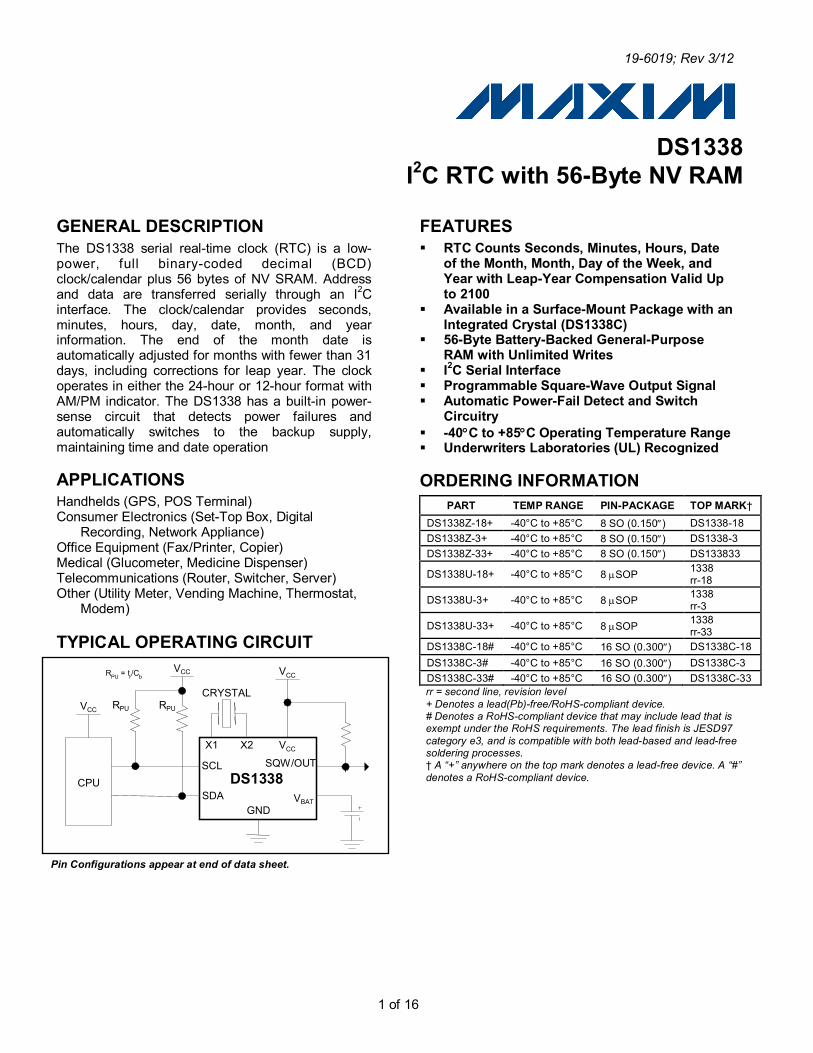
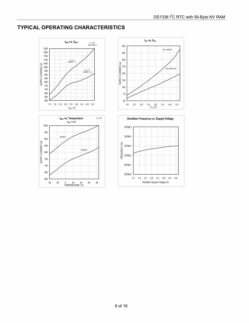
1 of 16 GENERAL DESCRIPTION The DS1338 serial real-time clock (RTC) is a low- power, full binary-coded decimal (BCD) clock/calendar plus 56 bytes of NV SRAM. Address and data are transferred serially through an I 2 C interface. The clock/calendar provides seconds, minutes, hours, day, date, month, and year information. The end of the month date is automatically adjusted for months with fewer than 31 days, including corrections for leap year. The clock operates in either the 24-hour or 12-hour format with AM/PM indicator. The DS1338 has a built-in power- sense circuit that detects power failures and automatically switches to the backup supply, maintaining time and date operation APPLICATIONS Handhelds (GPS, POS Terminal) Consumer Electronics (Set-Top Box, Digital Recording, Network Appliance) Office Equipment (Fax/Printer, Copier) Medical (Glucometer, Medicine Dispenser) Telecommunications (Router, Switcher, Server) Other (Utility Meter, Vending Machine, Thermostat, Modem) TYPICAL OPERATING CIRCUIT FEATURES RTC Counts Seconds, Minutes, Hours, Date of the Month, Month, Day of the Week, and Year with Leap-Year Compensation Valid Up to 2100 Available in a Surface-Mount Package with an Integrated Crystal (DS1338C) 56-Byte Battery-Backed General-Purpose RAM with Unlimited Writes I 2 C Serial Interface Programmable Square-Wave Output Signal Automatic Power-Fail Detect and Switch Circuitry -40°C to +85°C Operating Temperature Range Underwriters Laboratories (UL) Recognized ORDERING INFORMATION PART TEMP RANGE PIN-PACKAGE TOP MARK† DS1338Z-18+ -40°C to +85°C 8 SO (0.150″) DS1338-18 DS1338Z-3+ -40°C to +85°C 8 SO (0.150″) DS1338-3 DS1338Z-33+ -40°C to +85°C 8 SO (0.150″) DS133833 DS1338U-18+ -40°C to +85°C 8 µSOP 1338 rr-18 DS1338U-3+ -40°C to +85°C 8 µSOP 1338 rr-3 DS1338U-33+ -40°C to +85°C 8 µSOP 1338 rr-33 DS1338C-18# -40°C to +85°C 16 SO (0.300″) DS1338C-18 DS1338C-3# -40°C to +85°C 16 SO (0.300″) DS1338C-3 DS1338C-33# -40°C to +85°C 16 SO (0.300″) DS1338C-33 rr = second line, revision level + Denotes a lead(Pb)-free/RoHS-compliant device. # Denotes a RoHS-compliant device that may include lead that is exempt under the RoHS requirements. The lead finish is JESD97 category e3, and is compatible with both lead-based and lead-free soldering processes. † A “+” anywhere on the top mark denotes a lead-free device. A “#” denotes a RoHS-compliant device. Pin Configurations appear at end of data sheet. DS1338 CPU V CC V CC V CC SDA SCL GND X2 X1 V CC R PU R PU CRYSTAL SQW/OUT V BAT i R PU = t r /C b DS1338 I 2 C RTC with 56-Byte NV RAM 19-6019; Rev 3/12
Transcript
1 of 16
GENERAL DESCRIPTION The DS1338 serial real-time clock (RTC) is a low-power, full binary-coded decimal (BCD) clock/calendar plus 56 bytes of NV SRAM. Address and data are transferred serially through an I2C interface. The clock/calendar provides seconds, minutes, hours, day, date, month, and year information. The end of the month date is automatically adjusted for months with fewer than 31 days, including corrections for leap year. The clock operates in either the 24-hour or 12-hour format with AM/PM indicator. The DS1338 has a built-in power-sense circuit that detects power failures and automatically switches to the backup supply, maintaining time and date operation APPLICATIONS Handhelds (GPS, POS Terminal) Consumer Electronics (Set-Top Box, Digital
Recording, Network Appliance) Office Equipment (Fax/Printer, Copier) Medical (Glucometer, Medicine Dispenser) Telecommunications (Router, Switcher, Server) Other (Utility Meter, Vending Machine, Thermostat,
Modem)
TYPICAL OPERATING CIRCUIT
FEATURES RTC Counts Seconds, Minutes, Hours, Date
of the Month, Month, Day of the Week, and Year with Leap-Year Compensation Valid Up to 2100
Available in a Surface-Mount Package with an Integrated Crystal (DS1338C)
56-Byte Battery-Backed General-Purpose RAM with Unlimited Writes
I2C Serial Interface Programmable Square-Wave Output Signal Automatic Power-Fail Detect and Switch
Circuitry -40°C to +85°C Operating Temperature Range Underwriters Laboratories (UL) Recognized ORDERING INFORMATION
PART TEMP RANGE PIN-PACKAGE TOP MARK† DS1338Z-18+ -40°C to +85°C 8 SO (0.150″) DS1338-18 DS1338Z-3+ -40°C to +85°C 8 SO (0.150″) DS1338-3 DS1338Z-33+ -40°C to +85°C 8 SO (0.150″) DS133833
DS1338U-18+ -40°C to +85°C 8 µSOP 1338 rr-18
DS1338U-3+ -40°C to +85°C 8 µSOP 1338 rr-3
DS1338U-33+ -40°C to +85°C 8 µSOP 1338 rr-33
DS1338C-18# -40°C to +85°C 16 SO (0.300″) DS1338C-18 DS1338C-3# -40°C to +85°C 16 SO (0.300″) DS1338C-3 DS1338C-33# -40°C to +85°C 16 SO (0.300″) DS1338C-33 rr = second line, revision level + Denotes a lead(Pb)-free/RoHS-compliant device. # Denotes a RoHS-compliant device that may include lead that is exempt under the RoHS requirements. The lead finish is JESD97 category e3, and is compatible with both lead-based and lead-free soldering processes. † A “+” anywhere on the top mark denotes a lead-free device. A “#” denotes a RoHS-compliant device.
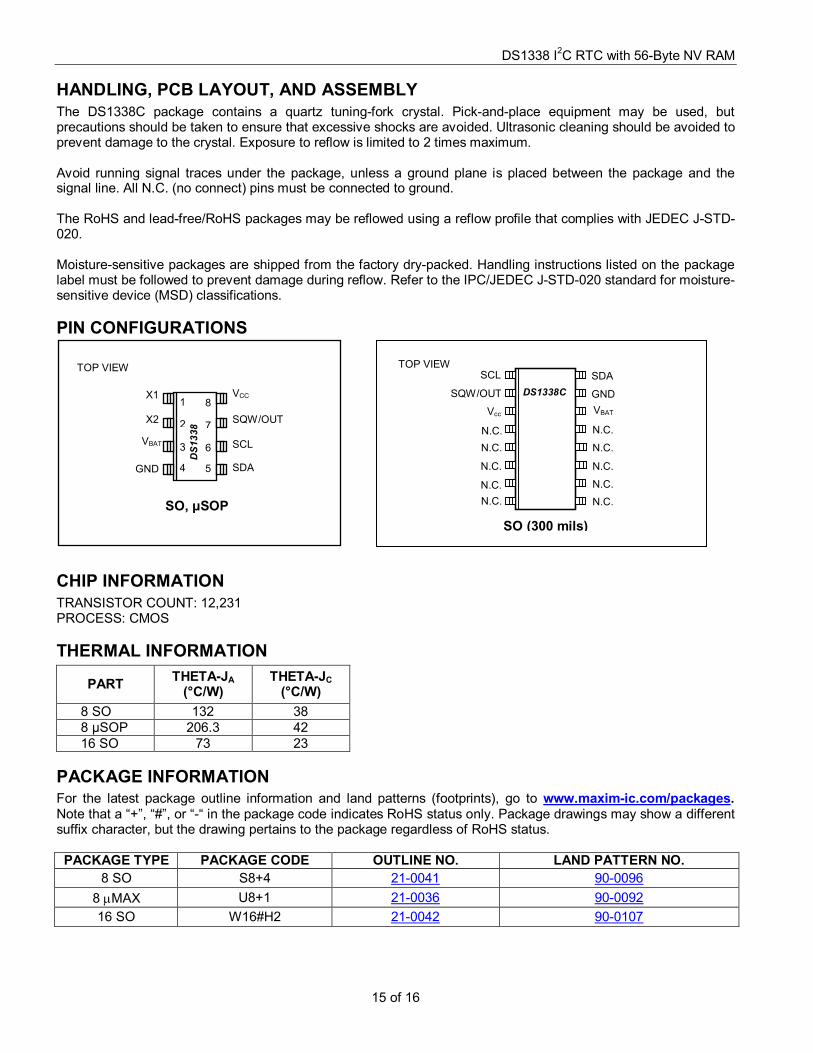
Pin Configurations appear at end of data sheet.
DS1338 CPU
V CC
V CC
V CC
SDA
SCL
GND
X2 X1
V CC
R PU R PU CRYSTAL
SQW/OUT
V BAT
i
R PU = t r /C b
DS1338 I2C RTC with 56-Byte NV RAM
19-6019; Rev 3/12
DS1338 I2C RTC with 56-Byte NV RAM
2 of 16
ABSOLUTE MAXIMUM RATINGS Voltage Range on Any Pin Relative to Ground………………………………………………………..……..-0.3V to +6.0V Operating Temperature Range…………………………………………………………………………..……-40°C to +85°C Storage Temperature Range………………………………………………………………………………...-55°C to +125°C Lead Temperature (soldering, 10s) ……….………………………………………………………………………. +260°C Soldering Temperature (reflow) ……………………………………………………………………………………. +260°C
Stresses beyond those listed under “Absolute Maximum Ratings” may cause permanent damage to the device. These are stress ratings only, and functional operation of the device at these or any other conditions beyond those indicated in the operational sections of the specifications is not implied. Exposure to the absolute maximum rating conditions for extended periods may affect device reliability.
RECOMMENDED DC OPERATING CONDITIONS (VCC = VCC(MIN) to VCC(MAX), TA = -40°C to +85°C, unless otherwise noted. Typical values are at TA = +25°C, unless otherwise noted.) (Note 1)
PARAMETER SYMBOL CONDITIONS MIN TYP MAX UNITS
Supply Voltage VCC DS1338-18 1.71 1.8 5.5
V DS1338-3 2.7 3.0 5.5 DS1338-33 3.0 3.3 5.5
Logic 1 VIH (Note 2) 0.7 x VCC VCC +
0.3 V
Logic 0 VIL (Note 2) -0.3 +0.3 x VCC V
Power-Fail Voltage VPF DS1338-18 1.51 1.62 1.71
V DS1338-3 2.45 2.59 2.70 DS1338-33 2.70 2.82 2.97
VBAT Input Voltage VBAT (Note 2) 1.3 3.0 3.7 V
DC ELECTRICAL CHARACTERISTICS (VCC = VCC(MIN) to VCC(MAX), TA = -40°C to +85°C, unless otherwise noted. Typical values are at VCC = TYP, TA = +25°C, unless otherwise noted.) (Note 1)
VBAT Leakage Current (VCC Active) IBATLKG 25 100 nA
DS1338 I2C RTC with 56-Byte NV RAM
3 of 16
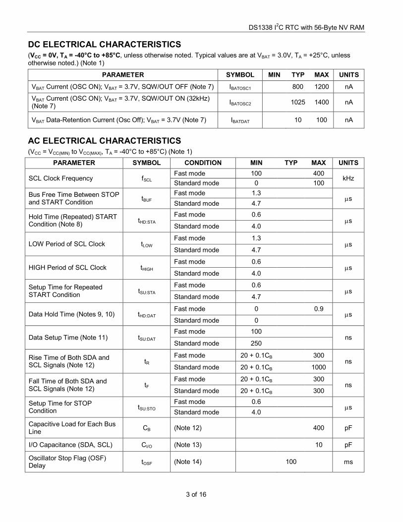
DC ELECTRICAL CHARACTERISTICS (VCC = 0V, TA = -40°C to +85°C, unless otherwise noted. Typical values are at VBAT = 3.0V, TA = +25°C, unless otherwise noted.) (Note 1)
PARAMETER SYMBOL MIN TYP MAX UNITS
VBAT Current (OSC ON); VBAT = 3.7V, SQW/OUT OFF (Note 7) IBATOSC1 800 1200 nA
VBAT Current (OSC ON); VBAT = 3.7V, SQW/OUT ON (32kHz) (Note 7) IBATOSC2 1025 1400 nA
VBAT Data-Retention Current (Osc Off); VBAT = 3.7V (Note 7) IBATDAT 10 100 nA
AC ELECTRICAL CHARACTERISTICS (VCC = VCC(MIN) to VCC(MAX), TA = -40°C to +85°C) (Note 1)
PARAMETER SYMBOL CONDITION MIN TYP MAX UNITS
SCL Clock Frequency fSCL Fast mode 100 400
kHz Standard mode 0 100
Bus Free Time Between STOP and START Condition tBUF
Fast mode 1.3 µs
Standard mode 4.7
Hold Time (Repeated) START Condition (Note 8) tHD:STA
Fast mode 0.6 µs
Standard mode 4.0
LOW Period of SCL Clock tLOW Fast mode 1.3
µs Standard mode 4.7
HIGH Period of SCL Clock tHIGH Fast mode 0.6
µs Standard mode 4.0
Setup Time for Repeated START Condition tSU:STA
Fast mode 0.6 µs
Standard mode 4.7
Data Hold Time (Notes 9, 10) tHD:DAT Fast mode 0 0.9
µs Standard mode 0
Data Setup Time (Note 11) tSU:DAT Fast mode 100
ns Standard mode 250
Rise Time of Both SDA and SCL Signals (Note 12) tR
Fast mode 20 + 0.1CB 300 ns
Standard mode 20 + 0.1CB 1000
Fall Time of Both SDA and SCL Signals (Note 12) tF
Fast mode 20 + 0.1CB 300 ns
Standard mode 20 + 0.1CB 300
Setup Time for STOP Condition tSU:STO
Fast mode 0.6 µs
Standard mode 4.0
Capacitive Load for Each Bus Line CB (Note 12) 400 pF
I/O Capacitance (SDA, SCL) CI/O (Note 13) 10 pF
Oscillator Stop Flag (OSF) Delay tOSF (Note 14) 100 ms
Warning: Negative undershoots below -0.3V while the part is in battery-backed mode may cause loss of data. Note 1: Limits at -40°C are guaranteed by design and not production tested. Note 2: All voltages are referenced to ground. Note 3: SCL only. Note 4: SDA and SQW/OUT. Note 5: ICCA—SCL clocking at max frequency = 400kHz. Note 6: Specified with the I2C bus inactive. Note 7: Measured with a 32.768kHz crystal attached to X1 and X2. Note 8: After this period, the first clock pulse is generated. Note 9: A device must internally provide a hold time of at least 300ns for the SDA signal (referred to the VIH(MIN) of the SCL signal) to
bridge the undefined region of the falling edge of SCL. Note 10: The maximum tHD:DAT need only be met if the device does not stretch the LOW period (tLOW) of the SCL signal. Note 11: A fast-mode device can be used in a standard-mode system, but the requirement tSU:DAT ≥ to 250ns must then be met. This is
automatically the case if the device does not stretch the LOW period of the SCL signal. If such a device does stretch the LOW period of the SCL signal, it must output the next data bit to the SDA line tR(MAX) + tSU:DAT = 1000 + 250 = 1250ns before the SCL line is released.
Note 12: CB—total capacitance of one bus line in pF. Note 13: Guaranteed by design. Not production tested. Note 14: The parameter tOSF is the time period the oscillator must be stopped for the OSF flag to be set over the voltage range of
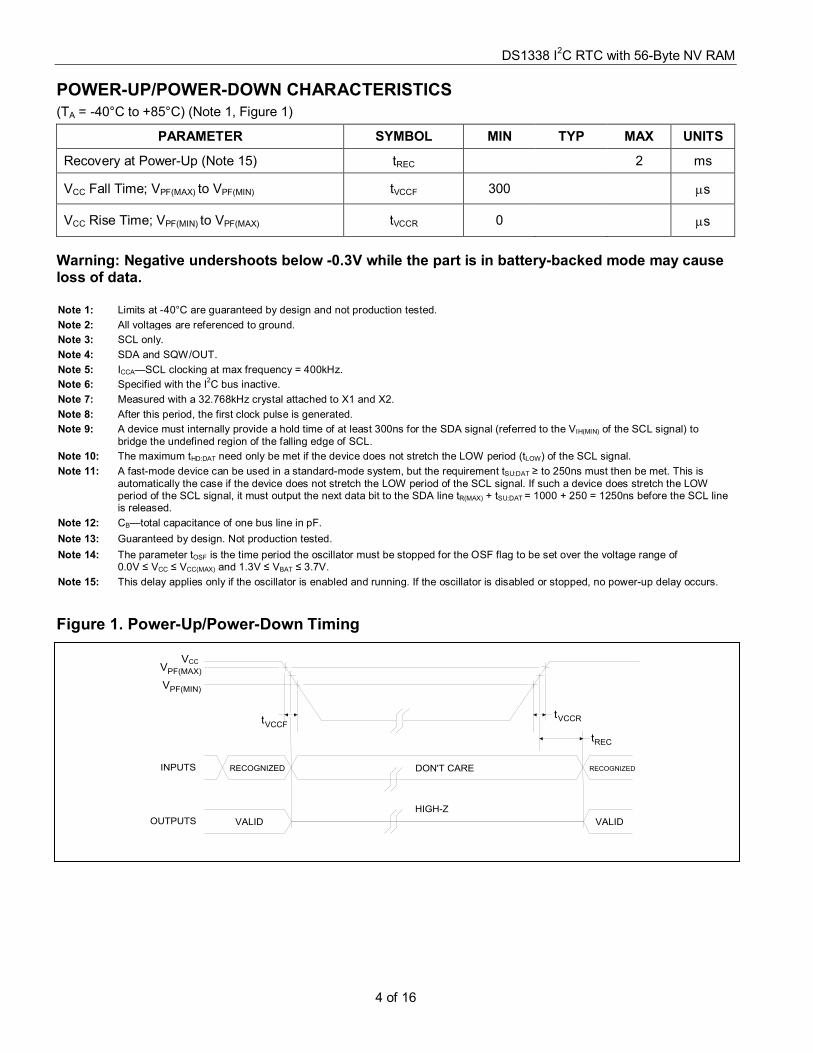
0.0V ≤ VCC ≤ VCC(MAX) and 1.3V ≤ VBAT ≤ 3.7V. Note 15: This delay applies only if the oscillator is enabled and running. If the oscillator is disabled or stopped, no power-up delay occurs. Figure 1. Power-Up/Power-Down Timing
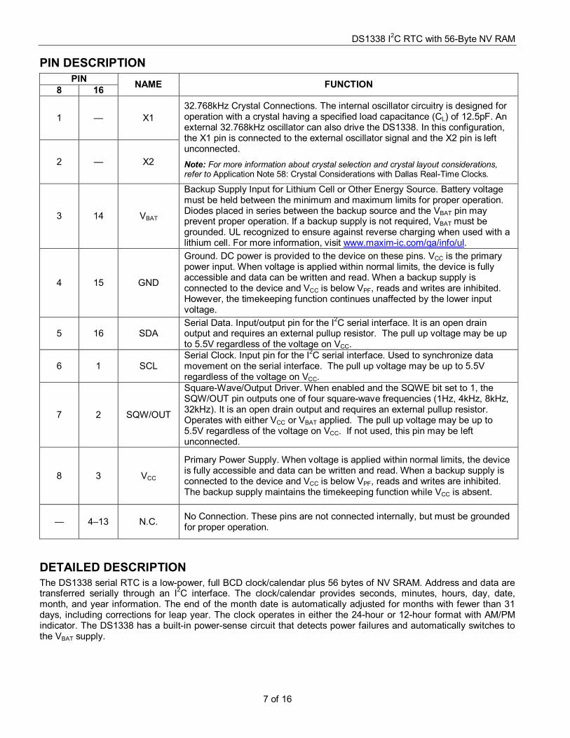
1 — X1 32.768kHz Crystal Connections. The internal oscillator circuitry is designed for operation with a crystal having a specified load capacitance (CL) of 12.5pF. An external 32.768kHz oscillator can also drive the DS1338. In this configuration, the X1 pin is connected to the external oscillator signal and the X2 pin is left unconnected. Note: For more information about crystal selection and crystal layout considerations, refer to Application Note 58: Crystal Considerations with Dallas Real-Time Clocks.
2 — X2
3 14 VBAT
Backup Supply Input for Lithium Cell or Other Energy Source. Battery voltage must be held between the minimum and maximum limits for proper operation. Diodes placed in series between the backup source and the VBAT pin may prevent proper operation. If a backup supply is not required, VBAT must be grounded. UL recognized to ensure against reverse charging when used with a lithium cell. For more information, visit www.maxim-ic.com/qa/info/ul.
4 15 GND
Ground. DC power is provided to the device on these pins. VCC is the primary power input. When voltage is applied within normal limits, the device is fully accessible and data can be written and read. When a backup supply is connected to the device and VCC is below VPF, reads and writes are inhibited. However, the timekeeping function continues unaffected by the lower input voltage.
5 16 SDA Serial Data. Input/output pin for the I2C serial interface. It is an open drain output and requires an external pullup resistor. The pull up voltage may be up to 5.5V regardless of the voltage on VCC.
6 1 SCL Serial Clock. Input pin for the I2C serial interface. Used to synchronize data movement on the serial interface. The pull up voltage may be up to 5.5V regardless of the voltage on VCC.
7 2 SQW/OUT
Square-Wave/Output Driver. When enabled and the SQWE bit set to 1, the SQW/OUT pin outputs one of four square-wave frequencies (1Hz, 4kHz, 8kHz, 32kHz). It is an open drain output and requires an external pullup resistor. Operates with either VCC or VBAT applied. The pull up voltage may be up to 5.5V regardless of the voltage on VCC. If not used, this pin may be left unconnected.
8 3 VCC
Primary Power Supply. When voltage is applied within normal limits, the device is fully accessible and data can be written and read. When a backup supply is connected to the device and VCC is below VPF, reads and writes are inhibited. The backup supply maintains the timekeeping function while VCC is absent.
— 4–13 N.C. No Connection. These pins are not connected internally, but must be grounded for proper operation.
DETAILED DESCRIPTION The DS1338 serial RTC is a low-power, full BCD clock/calendar plus 56 bytes of NV SRAM. Address and data are transferred serially through an I2C interface. The clock/calendar provides seconds, minutes, hours, day, date, month, and year information. The end of the month date is automatically adjusted for months with fewer than 31 days, including corrections for leap year. The clock operates in either the 24-hour or 12-hour format with AM/PM indicator. The DS1338 has a built-in power-sense circuit that detects power failures and automatically switches to the VBAT supply.
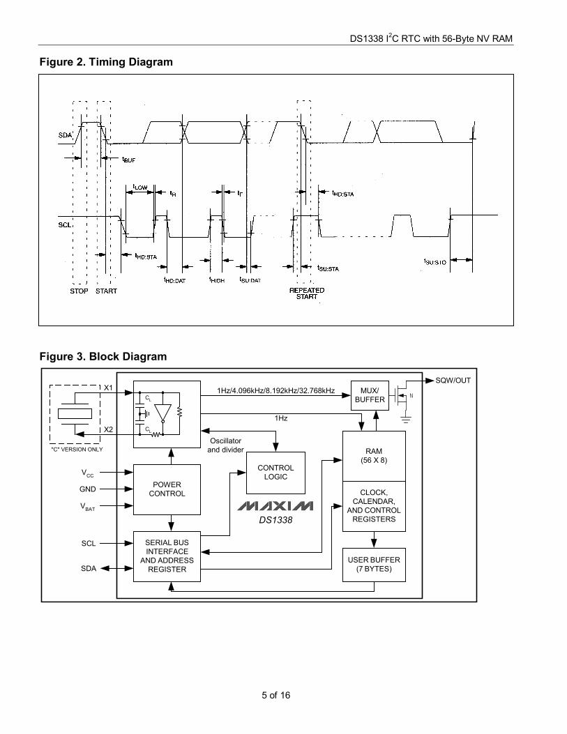
OPERATION The DS1338 operates as a slave device on the serial bus. Access is obtained by implementing a START condition and providing a device identification code, followed by data. Subsequent registers can be accessed sequentially until a STOP condition is executed. The device is fully accessible and data can be written and read when VCC is greater than VPF. However, when VCC falls below VPF, the internal clock registers are blocked from any access. If VPF is less than VBAT, the device power is switched from VCC to VBAT when VCC drops below VPF. If VPF is greater than VBAT, the device power is switched from VCC to VBAT when VCC drops below VBAT. The oscillator and timekeeping functions are maintained from the VBAT source until VCC is returned to nominal levels. The block diagram (Figure 3) shows the main elements of the DS1338. An enable bit in the seconds register controls the oscillator. Oscillator startup times are highly dependent upon crystal characteristics, PC board leakage, and layout. High ESR and excessive capacitive loads are the major contributors to long start-up times. A circuit using a crystal with the recommended characteristics and proper layout usually starts within 1 second. POWER CONTROL The power-control function is provided by a precise, temperature-compensated voltage reference and a comparator circuit that monitors the VCC level. The device is fully accessible and data can be written and read when VCC is greater than VPF. However, when VCC falls below VPF, the internal clock registers are blocked from any access. If VPF is less than VBAT, the device power is switched from VCC to VBAT when VCC drops below VPF. If VPF is greater than VBAT, the device power is switched from VCC to VBAT when VCC drops below VBAT. The registers are maintained from the VBAT source until VCC is returned to nominal levels (Table 1). After VCC returns above VPF, read and write access is allowed after tREC (Figure 1). On the first application of power to the device the time and date registers are reset to 01/01/00 01 00:00:00 (DD/MM/YY DOW HH:MM:SS). The CH bit in the seconds register will be set to a 0. Table 1. Power Control
OSCILLATOR CIRCUIT The DS1338 uses an external 32.768kHz crystal. The oscillator circuit does not require any external resistors or capacitors to operate. Table 2 specifies several crystal parameters for the external crystal. Figure 3 shows a functional schematic of the oscillator circuit. The startup time is usually less than 1 second when using a crystal with the specified characteristics. Table 2. Crystal Specifications*
PARAMETER SYMBOL MIN TYP MAX UNITS
Nominal Frequency fO 32.768 kHz
Series Resistance ESR 50 kΩ
Load Capacitance CL 12.5 pF *The crystal, traces, and crystal input pins should be isolated from RF generating signals. Refer to Application Note 58: Crystal Considerations for Dallas Real-Time Clocks for additional specifications.
DS1338 I2C RTC with 56-Byte NV RAM
9 of 16
CLOCK ACCURACY The accuracy of the clock is dependent upon the accuracy of the crystal and the accuracy of the match between the capacitive load of the oscillator circuit and the capacitive load for which the crystal was trimmed. Crystal frequency drift caused by temperature shifts creates additional error. External circuit noise coupled into the oscillator circuit can result in the clock running fast. Figure 4 shows a typical PC board layout for isolating the crystal and oscillator from noise. Refer to Application Note 58: Crystal Considerations with Dallas Real-Time Clocks for detailed information. DS1338C ONLY The DS1338C integrates a standard 32,768Hz crystal in the package. Typical accuracy at nominal VCC and +25°C is approximately 10ppm. Refer to Application Note 58 for information about crystal accuracy vs. temperature. Figure 4. Typical PC Board Layout for Crystal RTC AND RAM ADDRESS MAP Table 3 shows the address map for the RTC and RAM registers. The RTC registers and control register are located in address locations 00h to 07h. The RAM registers are located in address locations 08h to 3Fh. During a multibyte access, when the register pointer reaches 3Fh (the end of RAM space) it wraps around to location 00h (the beginning of the clock space). On an I2C START, STOP, or register pointer incrementing to location 00h, the current time and date is transferred to a second set of registers. The time and date in the secondary registers are read in a multibyte data transfer, while the clock continues to run. This eliminates the need to re-read the registers in case of an update of the main registers during a read. CLOCK AND CALENDAR The time and calendar information is obtained by reading the appropriate register bytes. See Figure 6 for the RTC registers. The time and calendar are set or initialized by writing the appropriate register bytes. The contents of the time and calendar registers are in the BCD format. Bit 7 of Register 0 is the clock halt (CH) bit. When this bit is set to 1, the oscillator is disabled. When cleared to 0, the oscillator is enabled. The clock can be halted whenever the timekeeping functions are not required, which minimizes VBAT current (IBATDAT) when VCC is not applied. The day-of-week register increments at midnight. Values that correspond to the day of week are user-defined but must be sequential (i.e., if 1 equals Sunday, then 2 equals Monday, and so on). Illogical time and date entries result in undefined operation. When reading or writing the time and date registers, secondary (user) buffers are used to prevent errors when the internal registers update. When reading the time and date registers, the user buffers are synchronized to the internal registers on any start or stop and when the register pointer rolls over to zero. The countdown chain is reset
LOCAL GROUND PLANE (LAYER 2)
CRYSTAL
X1
X2
GND
NOTE: AVOID ROUTING SIGNALS IN THE CROSSHATCHED AREA (UPPER LEFT-HAND QUADRANT) OF THE PACKAGE UNLESS THERE IS A GROUND PLANE BETWEEN THE SIGNAL LINE AND THE PACKAGE.
DS1338 I2C RTC with 56-Byte NV RAM
10 of 16
whenever the seconds register is written. Write transfers occur on the acknowledge from the DS1338. Once the countdown chain is reset, to avoid rollover issues the remaining time and date registers must be written within 1 second. The 1Hz square-wave output, if enabled, transitions high 500ms after the seconds data transfer, provided the oscillator is already running. The DS1338 runs in either 12-hour or 24-hour mode. Bit 6 of the hours register is defined as the 12-hour or 24-hour mode-select bit. When high, the 12-hour mode is selected. In the 12-hour mode, bit 5 is the AM/PM bit, with logic high being PM. In the 24-hour mode, bit 5 is the 20-hour bit (20–23 hours). If the 12/24-hour mode select is changed, the hours register must be re-initialized to the new format. On an I2C START, the current time is transferred to a second set of registers. The time information is read from these secondary registers, while the clock continues to run. This eliminates the need to re-read the registers in case of an update of the main registers during a read. Table 3. RTC and RAM Address Map
ADDRESS BIT 7 BIT 6 BIT 5 BIT 4 BIT 3 BIT 2 BIT 1 BIT 0 FUNCTION RANGE
03H 0 0 0 0 0 Day Day 1–7 04H 0 0 10 Date Date Date 01–31
05H 0 0 0 10 Month Month Month 01–12
06H 10 Year Year Year 00–99 07H OUT 0 OSF SQWE 0 0 RS1 RS0 Control
08H–3FH RAM 56 x 8 00H–FFH
Note: Bits listed as “0” always read as a 0.
DS1338 I2C RTC with 56-Byte NV RAM
11 of 16
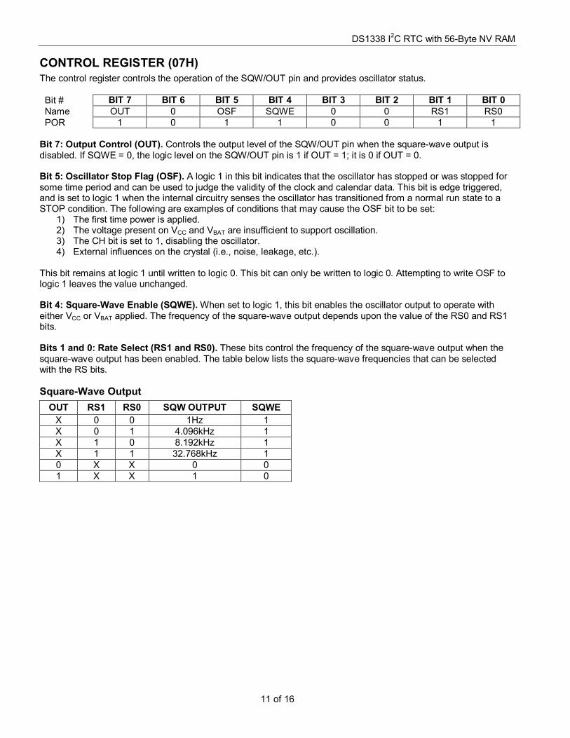
CONTROL REGISTER (07H) The control register controls the operation of the SQW/OUT pin and provides oscillator status. Bit # BIT 7 BIT 6 BIT 5 BIT 4 BIT 3 BIT 2 BIT 1 BIT 0 Name OUT 0 OSF SQWE 0 0 RS1 RS0 POR 1 0 1 1 0 0 1 1
Bit 7: Output Control (OUT). Controls the output level of the SQW/OUT pin when the square-wave output is disabled. If SQWE = 0, the logic level on the SQW/OUT pin is 1 if OUT = 1; it is 0 if OUT = 0. Bit 5: Oscillator Stop Flag (OSF). A logic 1 in this bit indicates that the oscillator has stopped or was stopped for some time period and can be used to judge the validity of the clock and calendar data. This bit is edge triggered, and is set to logic 1 when the internal circuitry senses the oscillator has transitioned from a normal run state to a STOP condition. The following are examples of conditions that may cause the OSF bit to be set:
1) The first time power is applied. 2) The voltage present on VCC and VBAT are insufficient to support oscillation. 3) The CH bit is set to 1, disabling the oscillator. 4) External influences on the crystal (i.e., noise, leakage, etc.).
This bit remains at logic 1 until written to logic 0. This bit can only be written to logic 0. Attempting to write OSF to logic 1 leaves the value unchanged. Bit 4: Square-Wave Enable (SQWE). When set to logic 1, this bit enables the oscillator output to operate with either VCC or VBAT applied. The frequency of the square-wave output depends upon the value of the RS0 and RS1 bits. Bits 1 and 0: Rate Select (RS1 and RS0). These bits control the frequency of the square-wave output when the square-wave output has been enabled. The table below lists the square-wave frequencies that can be selected with the RS bits. Square-Wave Output
OUT RS1 RS0 SQW OUTPUT SQWE X 0 0 1Hz 1 X 0 1 4.096kHz 1 X 1 0 8.192kHz 1 X 1 1 32.768kHz 1 0 X X 0 0 1 X X 1 0
DS1338 I2C RTC with 56-Byte NV RAM
12 of 16
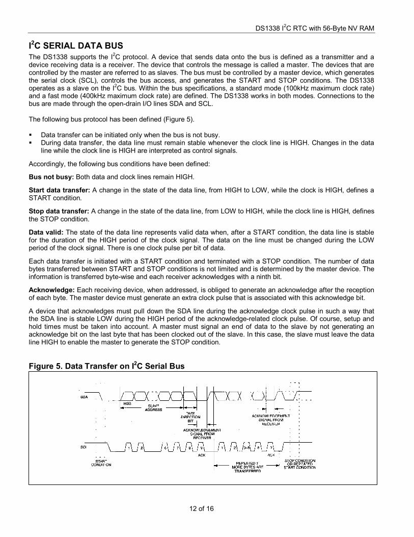
I2C SERIAL DATA BUS The DS1338 supports the I2C protocol. A device that sends data onto the bus is defined as a transmitter and a device receiving data is a receiver. The device that controls the message is called a master. The devices that are controlled by the master are referred to as slaves. The bus must be controlled by a master device, which generates the serial clock (SCL), controls the bus access, and generates the START and STOP conditions. The DS1338 operates as a slave on the I2C bus. Within the bus specifications, a standard mode (100kHz maximum clock rate) and a fast mode (400kHz maximum clock rate) are defined. The DS1338 works in both modes. Connections to the bus are made through the open-drain I/O lines SDA and SCL. The following bus protocol has been defined (Figure 5). Data transfer can be initiated only when the bus is not busy. During data transfer, the data line must remain stable whenever the clock line is HIGH. Changes in the data
line while the clock line is HIGH are interpreted as control signals.
Accordingly, the following bus conditions have been defined:
Bus not busy: Both data and clock lines remain HIGH.
Start data transfer: A change in the state of the data line, from HIGH to LOW, while the clock is HIGH, defines a START condition.
Stop data transfer: A change in the state of the data line, from LOW to HIGH, while the clock line is HIGH, defines the STOP condition.
Data valid: The state of the data line represents valid data when, after a START condition, the data line is stable for the duration of the HIGH period of the clock signal. The data on the line must be changed during the LOW period of the clock signal. There is one clock pulse per bit of data.
Each data transfer is initiated with a START condition and terminated with a STOP condition. The number of data bytes transferred between START and STOP conditions is not limited and is determined by the master device. The information is transferred byte-wise and each receiver acknowledges with a ninth bit.
Acknowledge: Each receiving device, when addressed, is obliged to generate an acknowledge after the reception of each byte. The master device must generate an extra clock pulse that is associated with this acknowledge bit.
A device that acknowledges must pull down the SDA line during the acknowledge clock pulse in such a way that the SDA line is stable LOW during the HIGH period of the acknowledge-related clock pulse. Of course, setup and hold times must be taken into account. A master must signal an end of data to the slave by not generating an acknowledge bit on the last byte that has been clocked out of the slave. In this case, the slave must leave the data line HIGH to enable the master to generate the STOP condition. Figure 5. Data Transfer on I2C Serial Bus
DS1338 I2C RTC with 56-Byte NV RAM
13 of 16
Depending upon the state of the R/W bit, two types of data transfer are possible: 1) Data transfer from a master transmitter to a slave receiver. The master transmits the first byte (the slave
address). Next follows a number of data bytes. The slave returns an acknowledge bit after each received byte. Data is transferred with the most significant bit (MSB) first.
2) Data transfer from a slave transmitter to a master receiver. The master transmits the first byte (the slave
address). The slave then returns an acknowledge bit, which is followed by the slave transmitting a number of data bytes. The master returns an acknowledge bit after all received bytes other than the last byte. At the end of the last received byte, a “not acknowledge” is returned. The master device generates all of the serial clock pulses and the START and STOP conditions. A transfer is ended with a STOP condition or with a repeated START condition. Since a repeated START condition is also the beginning of the next serial transfer, the bus is not released. Data is transferred with the most significant bit (MSB) first.
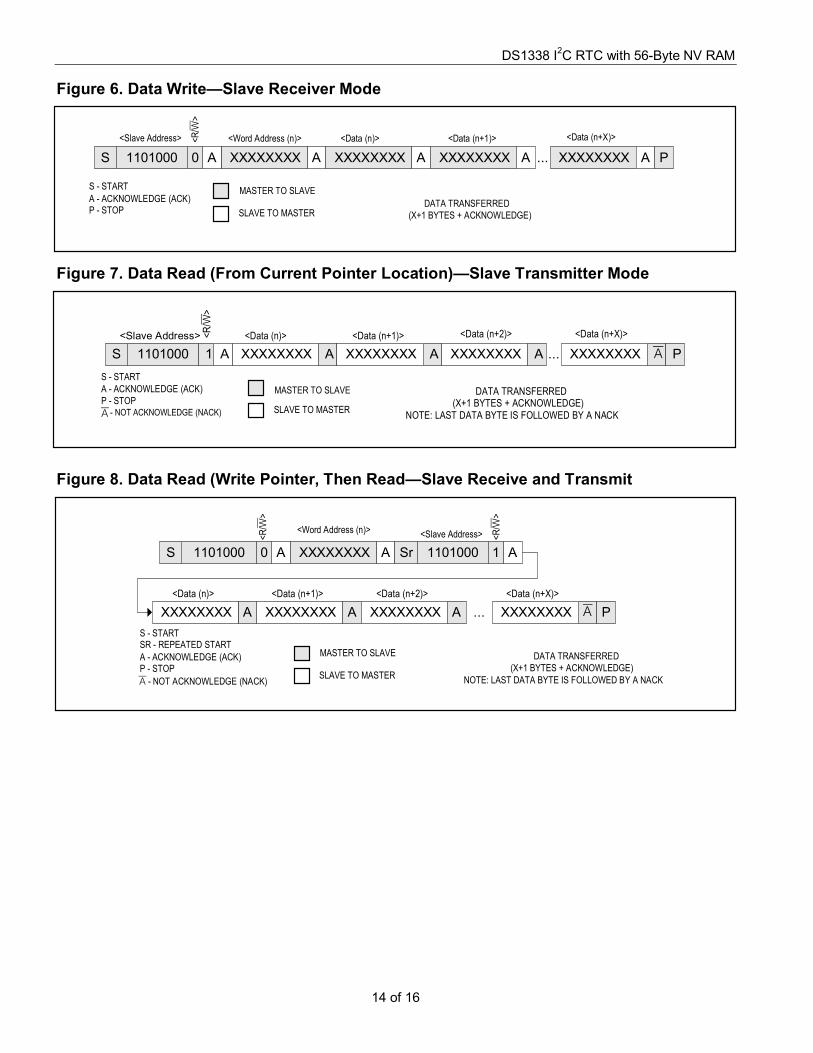
The DS1338 can operate in the following two modes: 1) Slave receiver mode (write mode): Serial data and clock are received through SDA and SCL. An
acknowledge bit is transmitted after each byte is received. START and STOP conditions are recognized as the beginning and end of a serial transfer. Hardware performs address recognition after reception of the slave address and direction bit (Figure 6). The slave address byte is the first byte received after the master generates the START condition. The slave address byte contains the 7-bit DS1338 address—1101000—followed by the direction bit (R/W), which, for a write, is 0. After receiving and decoding the slave address byte, the slave outputs an acknowledge on the SDA line. After the DS1338 acknowledges the slave address and write bit, the master transmits a register address to the DS1338. This sets the register pointer on the DS1338, with DS1338 acknowledging the transfer. The master may then transmit zero or more bytes of data, with the DS1338 acknowledging each byte received. The register pointer increments after each data byte is transferred. The master generates a STOP condition to terminate the data write.
2) Slave transmitter mode (read mode): The first byte is received and handled as in the slave receiver mode.
However, in this mode, the direction bit indicates that the transfer direction is reversed. The DS1338 transmits serial data on SDA while the serial clock is input on SCL. START and STOP conditions are recognized as the beginning and end of a serial transfer (Figure 7). The slave address byte is the first byte received after the master generates the START condition. The slave address byte contains the 7-bit DS1338 address—1101000—followed by the direction bit (R/W), which, for a read, is 1. After receiving and decoding the slave address byte, the slave outputs an acknowledge on the SDA line. The DS1338 then starts transmitting data using the register address pointed to by the register pointer. If the register pointer is not set before the initiation of a read mode, the first address that is read is the last one stored in the register pointer. The register pointer is incremented after each byte is transferred. The DS1338 must receive a “not acknowledge” to end a read.
DS1338 I2C RTC with 56-Byte NV RAM
14 of 16
Figure 6. Data Write—Slave Receiver Mode
Figure 7. Data Read (From Current Pointer Location)—Slave Transmitter Mode Figure 8. Data Read (Write Pointer, Then Read—Slave Receive and Transmit
... A XXXXXXXX A 1101000 S 1 XXXXXXXX A XXXXXXXX XXXXXXXX A P <Data (n+2)> <Data (n+X)>
A S - START A - ACKNOWLEDGE (ACK) P - STOP A - NOT ACKNOWLEDGE (NACK)
<R/W
>
DATA TRANSFERRED (X+1 BYTES + ACKNOWLEDGE)
NOTE: LAST DATA BYTE IS FOLLOWED BY A NACK
<Slave Address> <Data (n)> <Data (n+1)>
MASTER TO SLAVE
SLAVE TO MASTER
... A XXXXXXXX XXXXXXXX A XXXXXXXX A XXXXXXXX A P S - START SR - REPEATED START A - ACKNOWLEDGE (ACK) P - STOP
A - NOT ACKNOWLEDGE (NACK)
DATA TRANSFERRED (X+1 BYTES + ACKNOWLEDGE)
NOTE: LAST DATA BYTE IS FOLLOWED BY A NACK
A XXXXXXXX A 1101000 S 0
<R/W
>
<Word Address (n)>
A 1101000 Sr 1
<R/W
>
<Slave Address>
<Data (n)> <Data (n+1)> <Data (n+2)> <Data (n+X)>
MASTER TO SLAVE
SLAVE TO MASTER
... A XXXXXXXX A S 0 XXXXXXXX A XXXXXXXX A XXXXXXXX A P
HANDLING, PCB LAYOUT, AND ASSEMBLY The DS1338C package contains a quartz tuning-fork crystal. Pick-and-place equipment may be used, but precautions should be taken to ensure that excessive shocks are avoided. Ultrasonic cleaning should be avoided to prevent damage to the crystal. Exposure to reflow is limited to 2 times maximum. Avoid running signal traces under the package, unless a ground plane is placed between the package and the signal line. All N.C. (no connect) pins must be connected to ground. The RoHS and lead-free/RoHS packages may be reflowed using a reflow profile that complies with JEDEC J-STD-020. Moisture-sensitive packages are shipped from the factory dry-packed. Handling instructions listed on the package label must be followed to prevent damage during reflow. Refer to the IPC/JEDEC J-STD-020 standard for moisture-sensitive device (MSD) classifications. PIN CONFIGURATIONS CHIP INFORMATION TRANSISTOR COUNT: 12,231 PROCESS: CMOS THERMAL INFORMATION
PART THETA-JA (°C/W)
THETA-JC (°C/W)
8 SO 132 38 8 μSOP 206.3 42 16 SO 73 23
PACKAGE INFORMATION For the latest package outline information and land patterns (footprints), go to www.maxim-ic.com/packages. Note that a “+”, “#”, or “-“ in the package code indicates RoHS status only. Package drawings may show a different suffix character, but the drawing pertains to the package regardless of RoHS status. PACKAGE TYPE PACKAGE CODE OUTLINE NO. LAND PATTERN NO.
8 SO S8+4 21-0041 90-0096 8 µMAX U8+1 21-0036 90-0092 16 SO W16#H2 21-0042 90-0107
Modified the Features bullet to indicate that battery-backed RAM has unlimited writes. 1
Removed leaded part numbers from the Ordering Information table. 1 Removed the pullup resistor voltage spec from the Recommended DC Operating Conditions table and added it to the pin descriptions. 2, 7
Updated the block diagram (Figure 3) to show that SQW is open drain. 5 Added the initial POR state for time and date registers in the Power Control section. 8
Added text to explain the use of the oscillator bit to control battery current in the Clock and Calendar section. 9
9/11
Updated the Absolute Maximum Ratings, Recommended DC Operating Conditions, DC Electrical Characteristics, Power Control, Oscillator Circuit, Table 3, Handling, PBB Layout, and Assembly, Thermal Information, and Package Information.
2, 8, 10, 15
3/12 Corrected the CH bit POR condition from 1 to 0 in the Power Control section 8