66


2 02 6
I30
6 6
DSP-Based Canadian Timecode ReceiverPart 1: Identifying DSP TechniquesDavid Tweed
On- and Off-Hook Caller ID Using DSPDave Ryan eLJ Asher Hazanchuk
PC Telephone InterfaceChris Sakkas
Embedding the ARM7500Part 2: Programming an Embedded ComputerArt Sobel
A Winning Proposition
q MicroSeriesMachine VisionPart 1: Industrial InspectionHugh An&n
q From the BenchIt Can’t Be A RobotPart 1: There are No Arms and Legs
CROSSPOINT DATA SWITCH ICIMP has announced a digital crosspoint switch IC,
accommodating 256 x 256 channels. The IMP8980D is aCMOS device that switches digital datastreams such aspulse code modulated (KM) voice, video, or data signals.It establishes a path between any input and output overits internal ST-Bus (Serial Telecom Bus). Uses includedigital exchange, PBX, and central-office applications.
To support 256 channels, the IMP8980D has eighteach ST-Bus I/O pins. Via time-division multiplexing,the component-level 2048-kbps ST-Bus supports 32 log-ical data channels at 64 kbps at each device I/O pin.ST-Bus bit rate is divided into 8000 frames with 32 chan-nels per frame.
In the Message mode, the system microcontroller canpass data onto an output channel. In the nonblockingSwitching mode, the output can specify its input-chan-nel data source. Multiple outputs can share an input,which is useful in message-broadcast applications.
A system microprocessor makes switched connec-tions, writes data to output channels, and can receivedata from input channels. In addition, the system micro-
Edited by Harv Weiner
controller can concurrently read input-channel data andwrite data to ST-Bus channel outputs. Large logical-switchstructures are possible since the IMP8980D can set out-puts into a high-impedance state on a per-channel basis.
Pricing for the 44-pin PLCC IMP8980DP and 40-pinDIP IMP8980DE starts at $7.70 in quantity.
IMP, Inc.2830 N. First St.San Jose, CA 95134-2071(408) 432-9100 l Fax: (408) 434-0335www.impweb.com #501
- 3 PAR (32 BITS MAX)- 32K RAM. EXP 64M-STANDARD PC BUS- LCD. KBD PORT- BATT. BACK. RTC- IRQO-15 (8259 X2)- 0237 DMA 8253 TMR-BUILT-IN LED DISP.-UPTOBMEGROM-CMOS NVRAM
$95 ?g-$fUNNERSAL
PROGRAMMER-DOES 8 MEG EPROMS-CMOS, EE, FLASH, NVRAM- EASIER TO USE THAN MOST- POWERFUL SCRIPT ABILITY- MICROCONT. ADAPTERS- PLCC, MINI-DIP ADAPTERS-SUPER FAST ALGORITHMS
USE TURBO C,BASIC, MASM
RUNS DOS ANDWINDOWS
EVAL KIT $295
OTHER PRODUCTS:8088 SINGLE BOARD COMPUTER . . . . . . . OEM $27... l 95PC FLASH/ROM DISKS . . . . . 7516 BIT 16 CHAN ADC-DA
128K-18M) . . . . . . . . . . . . . . . . . . 21C CARD . . . . . . . . . . . . . . . . . . . . . %...I95
WATCHDOG (REBOOTS PC ON HANGUP) . . . . . 27 . . . . . 95l EVAL KITS INCLUDE MANUAL
BRACKET AND SOFTWARE. v) MVS BOX 8505 YR LIMITED WARRANTY
FREE SHIPPINGHRS: MON-FRI IOAM-BPM EST a
$ MERRIMACK, NH. (508) 792 9507
Contacting Circuit CellarWe at Circuit Cellar INKencourage communication between
our readers and our staff, so we have made every effort to makecontacting us easy. We prefer electronic communications, butfeel free to use any of the following:
Mail: Letters to the Editor may be sent to:Editor,Circuit Cellar INK,4 Park St.,Vernon, CT 06066.
Phone: Direct all subscription inquiries to (800) 269-6301.Contact our editorial offices at (860) 875-2199.
Fax: All faxes may be sent to (860) 871-0411.
BBS: All of our editors and regular authors frequent the CircuitCellar BBS and are available to answer questions. Call(860) 871-1988 with your modem (300-14.4k bps, 8Nl).
Internet: Letters to the editor may be sent to [email protected]. Send new subscription orders, renewals, and ad-dress changes to [email protected]. Be sure toinclude your complete mailing address and return E-mailaddress in all correspondence. Author E-mail addresses(when available) may be found at the end of each article.For more information. send E-mail to infoQcircellar.com.
WWW: Point your browser to www.circellar.com.#103
6 Issue 93 June 1997 Circuit Cellar INKm
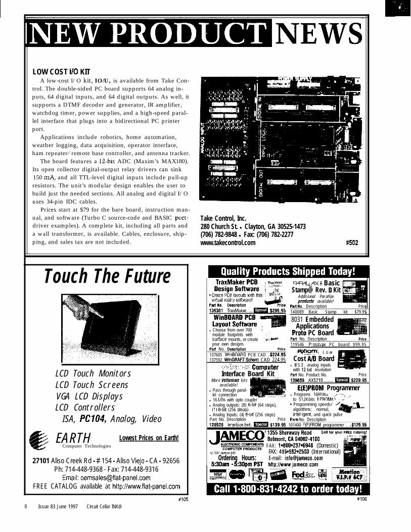
LOW COST 110 KITA low-cost I/O kit, IO/U, is available from Take Con-
trol. The double-sided PC board supports 64 analog in-puts, 64 digital inputs, and 64 digital outputs. As well, itsupports a DTMF decoder and generator, IR amplifier,watchdog timer, power supplies, and a high-speed paral-lel interface that plugs into a bidirectional PC printerport.
Applications include robotics, home automation,weather logging, data acquisition, operator interface,ham repeater/remote base controller, and antenna tracker.
The board features a 1%bit ADC (Maxim’s MAX180).Its open collector digital-output relay drivers can sink150 mA, and all TTL-level digital inputs include pull-upresistors. The unit’s modular design enables the user tobuild just the needed sections. All analog and digital I/Ouses 34-pin IDC cables.
Prices start at $79 for the bare board, instruction man-ual, and software (Turbo C source-code and BASIC port-driver examples). A complete kit, including all parts anda wall transformer, is available. Cables, enclosure, ship-ping, and sales tax are not included.
Take Control, Inc.280 Church St. l Clayton, GA 30525-1473(706) 782-9848 l Fax: (706) 782-2277www.takecontrol.com #502
Touch The Future
LCD Touch Mon i torsL C D T o u c h S c r e e n sV G A L C D D i s p l a y sLCD Contro l l ers
ISA, PC104, Ana log , V ideo
@ E A R T H Lowest Prices on Earth!d Computer Technologies
27101 Aliso Creek Rd - # 154 - Aliso Viejo - CA - 92656Ph: 714-448-9368 - Fax: 714-448-9316
Email: oemsales@flat-paneLcornFREE CATALOG available at http://www.flat-paneI.com
l Choose from over 700 !module footprints withsurface mounts, or createvour own desions
P.&i No. Descr~tion Price
137605 WinBOARD PCB CAD ..$224.95137592 WinDRAFT Schem CAD 224.95
Interface Board KitMore Velleman kits
a v a i l a b l e !l Pass through paral-
lel connectionl 16 I/OS with opto couplerl Analog outputs: (8) 6-bit (64 steps),
(1) 8-bit (256 steos)l Analog Inputs: (4j 8brt (256 steps)Parr No. Description Price
- Programming speeds/algorithms: normal,mtelligent, and quick pulse
PricePan No. Description128928 101400 E(E)PROM programmer . ..$129.95
JMECO’ ;~~%5,“n:pre~“9’4~;;~,oo CalI for Your FREE C-W
zRc FAX: 1*800*237~6948 (Domestic)0 1WJameco C/91 FAX: 415*592*2503 (International)
Ordering Hours: E-mail: info@jameco,com5:3Oam - 5:3Op http://www.jameco.com
PHL@:: ;z, BasicStamp@ Rev. 0 Kit
Additional Parallaxoroducts available!
Part ire. Description Price140089 Basic Stamp kit $79.95
8031 EmbeddedApplications
Proto PC BoardPart No. Description Price119546 Prototvpe PC board $99.95
~~~~~* L o w
Cost A/D Boardl 16 S.E. analog inputs
with 12.bit resolutionPart No. Product No. Price136688
E(E)PROM Programmerl Programs 16Kbits
to 512Kbits EPROMs{ “?
#105
8 Issue 83 June 1997 Circuit Cellar INK@

INFRARED TRANSCEIVERThe TFDTGOOO is a multimode integrated IR transceiver
module for data-communication systems. The transceiver sup-ports all IrDA speeds up to 4 Mbps, HP-SIR, and Sharp ASKmodes. Integrated into this tiny package are a photodiode, IRLED, and analog IC. A current-limiting resistor in series and aVc, bypass capacitor are the only external components requiredto implement a complete transceiver.
The transceiver uses a complete differential design for supe-rior interference rejection. It features 5-V operation and lowpower consumption. By integrating the receiver’s preamplifierand the transmitter’s driver stage, the TFDT6000 transceivercombines the functions of two ICs and eliminates a large num-ber of external components. A typical discrete implementationrequires up to nine separate components.
The transceiver is offered in a surface-mount epoxy resinpackage measuring 0.52” x 0.30” with a height of 0.23”. High-volume pricing is $4.50 each.
Temic Semiconductors2201 Laurelwood Rd. l Santa Clara, CA 95054-l 595(408) 567-8220 l Fax: (408) 567-8995 #503
#108Issue 93 June 1997 Circuit Cellar INK@

RS-485/RS-422 TRANSCEIVERS FAIL-SAFE OUTPUT GUARANTEES LOGIC 1 DURING SHORT OR OPEN CIRCUITEach item in the MAX3080-MAX3089 family of THE MAXIM WAY OTHER K-485 DEVICES
high-speed RS-485/RS-422 communications trans- +POOmVceivers includes one driver and one receiver. Thedevices feature fail-safe circuitry, guaranteeing alogic-high receiver output when the receiver inputs aare open or shorted. Thus, the receiver output is alogic-high if all transmitters on a terminated bus are d ,NTER?,NPITEdisabled (high impedance).
The MAX3080, ‘8 1, and ‘82 feature reduced slew-
~~ ~-i;p,T ~‘::r~,~
-2WmV trate drivers that minimize EM1 and reflections causedby improperly terminated cables, enabling error-freedata-transmission rates up to 115 kbps. The MAX3083,‘84, and ‘85 offer higher driver output slew-rate limits,allowing transmit speeds up to 500 kbps. The MAX3086,‘87, and ‘88 driver slew rates are unlimited, so transmitspeeds up to 10 Mbps are possible. The MAX3089 slewrate can be 115 kbps, 500 kbps, or 10 Mbps by driving aselector pin with a single tristate driver.
All devices have a ‘/R-unit-load receiver input imped-ance that enables up to 256 transceivers on the bus.Driver outputs are short-circuit-current limited and pro-
tected by thermal shutdown circuitry that puts them in ahigh-impedance state to avoid excessive power dissipa-tion.
The devices come in 8- and 14.pin plastic DIP and SOpackages. Prices start at $1.25 in quantity.
Maxim Integrated Products120 San Gabriel Dr.Sunnyvale, CA 94086(408) 737-7600 l Fax: (408) 737-7194www.maxim-ic.com #504
OVER/UNDER VOLTAGE PROTECTORThe “Smart” Protector Type 6 (SPPC-6) PC board
controls an offcard solid-state relay to disconnect a loadif the AC power-line voltage exceeds programmed limits.The nominal line voltage is set via an oncard DIP switch.High and low voltage limits are proportional to the pro-grammed voltage (i.e., 110-140 V when set for 125-Voperation, and 95-125 V with a 110-V line). Power avail-able for the controlled relay is 6 mA max., so a solid-state relay must be used. Load current depends on therelay rating.
A Microchip PIC 16C71 microprocessor, powered by arechargeable lOO-mAh NiCd battery, monitors the ACpower-line voltage. If the voltage exceeds limits, the
relay opens and the load disconnects. The circuit auto-matically resets itself and reconnects the load after 80 swhen the line voltage returns within limits. An on-cardcircuit trickle charges the NiCd battery.
The s-bit ADC output (proportional to monitoredvoltage) is broadcast as a serial RS-232 signal to enabledisplay and logging. A two-wire interface is used, andhandshaking with the receiver is not needed. SampleMS-DOS software is supplied.
The user can select the Protector response during apower outage. If a DIP switch is off, the microprocessorenters sleep mode to conserve battery power, but it con-tinues to monitor the AC line. When the switch is on,the microprocessor continues to broadcast the voltage (0,in this case) over the RS-232 line. This feature is usefulwhen outage and restore times need to be logged butbattery current is -30% higher. When power returns,reset is automatic.
A built-in test circuit simulates an out-of-limits linevoltage with a single-pole, normally open push-buttonswitch.
The SPPC-6 sells for $42.
TDL Electronics5260 Cochise Trail l Las Cruces, NM 88012-9736(505) 382-8175 l Fax: (505) 382-8810
Circuit Cellar INKm Issue 83 June 1997 11

FEATURESDSP-Based CanadianTimecode Receiver
On- and Off-Hook CallerID Using DSP
PC Telephone Interface
Embedding the ARM7500
TimecodeReceiver
David Tweed
Part 1: Identifying DSI?Techniques
lot has been writ-ten recently about
digital signal processing,especially since the advent
of low-cost general-purpose DSP chipslike the Texas Instruments TMS320series, the Motorola DSP56000, andthe Analog Devices ADSP-2101 family.Digital filtering and spectral analysishave been covered as well as high-levelapplication topics such as speech,music, image, and video compression.
But, with the nuts and bolts of finiteimpulse response (FIR) versus infiniteimpulse response (IIR) filters, or corre-lation functions, or discrete Fouriertransform (DFT) versus fast Fouriertransform (FFT), many people get lostin the details and mathematics.
In this two-part series, I want you togain a more intuitive feel for thesetopics. So, I skip (most of] the math,and concepts are presented graphically.I also discuss the practical tradeoffsassociated with using these techniquesin a real application.
Part 1 introduces the application andwalks through the high-level design toidentify the necessary DSP techniques.I examine two techniques-cross-corre-lation and FIR filtering-in detail.
In Part 2, I discuss the Fourier Trans-form and real-world issues that arise
12 Issue 93 June 1997 Circuit Cellar INK@
Voice :oo
Silence untilbeginning of
I I I0 100
next200 300 400
second500
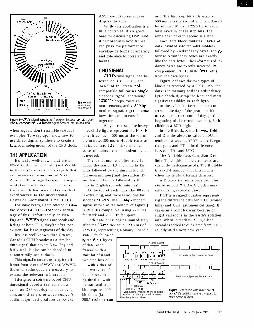
Figure l-CHU’s signal repeats each minute. Seconds :31-:39 containa Be/i 103~compatible FSK modem signal between the second ticks.
CHU’s time signal can befound on 3.330, 7.335, and14.670 MHz. It’s an AM-compatible full-carrier single-sideband signal, containingIOOO-Hz beeps, voice an-nouncements, and a 300-bpsmodem signal. Figure 1 shows
how the components fittogether.
As you can see, the heavywhen signals don’t resemble textbookexamples. To wrap up, I show how touse direct digital synthesis to create atimebase independent of the CPU clock.
THE APPLICATIONIt’s fairly well-known that station
lines of the figure represent the lOOO-Hztone. It comes in 500 ms at the top ofthe minute, 300 ms or double tones asindicated, and lo-ms ticks when avoice announcement or modem signalis needed.
WWV in Boulder, Colorado (and WWVHin Hawaii) broadcasts time signals thatcan be received over most of NorthAmerica. These signals contain compo-nents that can be decoded with rela-tively simple hardware to keep a clocksynchronized to the internationalUniversal Coordinated Time (UTC).
Figure 2 shows the two types ofblocks as received by a CPU. Once thedata is in memory and the redundancybytes checked, swap the least and mostsignificant nibbles in each byte.
In the A block, the 6 is a constant,DDD is the day of the year, and hh:mm:ss is the UTC time of day (at thebeginning of the current second). Eachnibble is a BCD digit.
In the B block, X is a bitwise field,and D is the absolute value of DUT intenths of a second. YYYY is the Grego-rian year, and TT is the differencebetween TAI and UTC.
The A nibble flags Canadian Day-light Time (this nibble’s contents arecurrently undocumented). The B nibbleis a serial number that incrementswhen the B-block format changes.
A B block transmits once per min-ute, at second :3 1. An A block trans-mits during seconds :32-:39.
DUT is a signed number represent-ing the difference between UTC (atomictime) and UT1 (astronomical time). Itvaries in a complex way because ofslight variations in the earth’s rotationrate. When it reaches kO.7 s, a leapsecond is added to or deleted from UTC,
2225 Hz, representing a binary 1 or idle usually at the next new year.state. It’s followedby ten 8-bit bytes 1
The announcement alternates be-tween the station ID and time in En-glish followed by the time in French(on even minutes) and the station IDand time in French followed by thetime in English (on odd minutes).
For some years, Heath offered a kit-the Model GClOOO-that took advan-tage of this. Unfortunately, in NewEngland, WWV’s signals are weak andfading at best. Plus, they’re often non-existent for large segments of the day.
At the top of each hour, the :00 toneis extra long, and there is no tone forseconds :Ol-:09. The 300-bps modemsignal shown at the bottom of Figure 1is Bell 103 compatible, using 2225 Hzfor mark and 2025 Hz for space.
Each data burst begins immediatelyafter the lo-ms tick with 123.3 ms of
It’s less well-known that Ottawa,Canada’s CHU broadcasts a similartime signal that covers New Englandfairly well. It also can be decoded toautomatically set a clock.
This signal’s structure is quite dif-ferent from those of WWV and WWVH.So, other techniques are necessary toextract the relevant information.
I designed a software-based CHUtime-signal decoder that runs on acommon DSP development board. Ituses an ordinary shortwave receiver’saudio output and produces an RS-232
ASCII output to set and/ordisplay the time.
While this application is alittle contrived, it’s a goodbase for discussing DSP. And,it demonstrates how far wecan push the performanceenvelope in terms of accuracyand tolerance to noise andfading.
CHU SIGNAL
mit. The last stop bit ends exactly500 ms into the second and is followedby another 10 ms of 2225 Hz to avoidfalse overrun of the stop bits. Theremainder of each second is silent.
Each data block contains 5 bytes ofdata (divided into ten 4-bit nibbles),followed by 5 redundancy bytes. The A-format redundancy bytes are exactlylike the data bytes. The B-format redun-dancy bytes are exactly inverted (l’s
complement, NOT, XOR OxFF, etc.)from the data bytes.
of data, eachframed with astart bit of 0 andtwo stop bits of 1.
With either ofthe two types ofdata blocks (A orB), the data withits start and stopbits requires 110bit times (i.e.,366.7 ms) to trans-
A Block Format
Redundancy Bytes Same as Data
Day of Year Hours Minutes Seconds
B Block Format
Redundancy Bytes are Data lnvelled
111 t t hii+ TAIDlff%?RX
UT1 DifferenceSign of UT1 (O=+)
Leap-Second Warning: Is will be addedLeap-Second Warning: 1s will be deleted
Even Parity for this Nibble
Figure 2-Once the data bytes are re-ceived, the nibbles must be swapped tomake sense of them.
Circuit Cellar INK@ Issue 83 June 1997 13

Audio In
55.0 55.1 55.2 55.3 55.4 55.5 55.6 55.7 55.8 55.9 56.0 56.1 56.2
ASCII Out
Figure 3--The A.%// output of the receiver ends jusf as the corresponding second begins.
A BETTER MOUSETRAP RS-232 OUTPUTSuppose you want to build a clock
that sets itself to the CHU signal likethe Heathkit clock does to the WWVsignal. And, you want to see how pre-cise you can get this signal.
The Heathkit clock guarantees10.ms accuracy when its Hi Spec lightis on, but I think submillisecond accu-racy is possible. I want a lot of infor-mation out of the audio signal despiteits noisiness.
Under most conditions, CHU offersa stronger signal than WWV to NewEngland. However, it’s still subject tosevere fading.
The clock should provide continuousoutput regardless of the radio signal’scondition, while keeping the best pos-sible accuracy. That’s why I didn’t justuse a $15 modem.
FUNCTIONAL SPECIFICATIONI wanted to generate an RS-232 out-
put that gives the time of day as anASCII string every second, based onthe signal received from CHU.
This string has a fixed length of18 bytes and is transmitted so the lastbyte ends at the time represented bythe string (see Figure 3). The screenappears in sync with the audio, but Istarted transmitting the string 18 char-acter times before the represented time.
ACCURACYSince the signal isn’t always avail- The local timebase should be as
able, the product needs a local timebase. accurate as possible within the limitsI wanted to avoid RF, so I used the imposed by the radio link and receiver.audio output of a shortwave receiver. The lOOO-Hz tones give a basic 1-pps
The audio input isfrom the headphonejack of a general-cover-age shortwave receiver,which gives a 1 -VRMSsignal. The DSP evalu-ation board’s audioinput should acceptthis directly.
I
TP3054Audio Codec
Jack ,II
ADSP-2101 1 _.,“._. ISPORT0 I
Integer DSP 1I’
I1
Figure 4--The complete timereceiver has a radio, fhe DSPeval board, and a computer orferminal fo display the time. TheADSP-2101 EZ-Lab eval boardincludes the DSP, a boot PROM,a voice-grade audio codec, anda four-channel DAC. The DSPoutline offers a tentafive soff-ware-dataflow diagram.
The output signal is RS-232C, usingASCII characters in an 8Nl configura-tion. The data rate would range be-tween 300 and 9600 bps.
Using C pr i n t f ( 1 notation, theoutput string is:
\r%4d %3d %Zd:%02d:%02d
where the individual fields are year,day, hours, minutes, and seconds UTC(using 24-h notation). \ r represents abare CR.
When observed on a screen or emula-tor, the time display updates in placeonscreen, leaving the cursor at the endof the string between updates.
(pulse per second) indication. Depend-ing on how accurately I identify thetones’ start and stop transitions, I canset the local timebase to within a fewmilliseconds.
By discriminating individual cyclesof the 1000 Hz, I can get it to around1 ms. And, if I can accurately measurethe tone’s relative phase angle, I mightget O.l-ms or less error.
However, the radio-path lengthbetween Ottawa and eastern Massachu-setts is -700 km. And, it can vary by-10% as the ionosphere varies in heightand reflectivity.
At 300,000 km/s, the path delay is-2.2 kO.2 ms. So, the accuracy goalshould be -1 .O-ms maximum instanta-neous error.
TOP-DOWN DESIGNOnce the product’s task is set, con-
sider which technologies to use.I need to decode audio tones at 1000,
2025, and 2225 Hz. I also need a localtimebase to generate ASCII outputmessages which synchronizes withCHU’s signal when it is available.
While analog filters along with I’LL(phase-locked loop) circuits handle tonedecoding and the local timebase, theyare rather inflexible for trying differentalgorithms or if the functional require-ments change. Also, getting everythingto work together optimally is a com-plex calibration process.
To demonstrate DSP techniqueswith an off-the-shelf evaluation board,I chose an all-software implementation.
m
1 LaptopComputer 1 ~
III
27512Boot PROM
IMemory Bus I
II
4-Channel DAC Debug II
ADSP-2101Evaluation Board
14 Issue 83 June 1997 Circuit Cellar INK@

16
XNHANCED SOLID STATEDRIVE - $105*
4M Total, Either Drive Bootable‘h Card 2 Disk Emulator
Flash System Software IncludedFLASH & SRAM Customs too
486 66MHz SINGLE CARDCOMPUTER - $335*
Up to 2.5Meg Flash/Sram driveCompact-XT height ‘h card size
Industry Standard PC-l 04 portL2 cache to 64K-DRAM to 16Meg
Dual IDE/Floppy connectors
All Tempustech VMAXB products arePC Bus Compatible. Made in the
U.S.A., 30 Day Money Back Guarantee*Qty 1, Qty breaks start at 5 pieces.
TEMPUSTECH, INC.TEL: (800) 634-0701FAX: (941) 643-4981
E-Mail: [email protected]: www.tempustech.com
Fax forfast response!
295 Airport RoadNaples, FL 34104
#llO
Issue 83 June 1997 Circuit Cellar INK”
Figure 4 shows the complete hard-ware of the time receiver. It comprisesa Realistic DX-380 receiver, AnalogDevices’ EZ-Lab board for the ADSP-2101, and a TRS-80 Model 100 laptop.
Within the dotted line is the blockdiagram of the DSP evaluation board.It includes an audio codec for the A/Dconversion. An RS-232 level converteron serial port 1 (SPORTl) generates thecorrect voltages for the output signal.
The four-channel DAC connects toan oscilloscope for algorithm develop-ment and debugging. There, it graphi-cally indicates the DSP’s real-timeactivity.
The software takes in 8000 audiosamples per second-more than suffi-cient to handle the bandwidth. It gen-erates ASCII output messages as well.
In between, it detects tones anddecodes CHU signal’s data. Using thisinformation, it establishes a local time-base relative to the CPU’s crystal. Thetimebase then drives the output-mes-sage generator.
Figure 4 illustrates the requiredcomponents and how they interact. Ifully develop this diagram after dis-cussing possible techniques for tonedetection and establishing a timebase.
TONE DETECTION
receiver’s operation. Because I want
From this diagram, you see thattone detection plays a major role in the
high accuracy, it’s important to deter-mine the existence or nonexistence oftones and to find when they begin andend-down to a single cycle or less.
Many people believe this is whatFFTs are for. But, the FFT is mostuseful when you’re looking for one ormore tones but don’t know their fre-quency. It’s overkill when looking fora tone at a particular frequency, and itisn’t particularly good at locating atone’s start and stop edges.
A Fourier Transform (FT) converts ablock of numbers representing signalsamples in time into the signal’s fre-quency components for that period. Itcan’t tell you whether a given compo-nent was there for the whole block oftime or only part of it.
The best you can do is see whetherthe component is present in one blockbut not another. This limits time reso-lution to the FFT’s block size.
So, you use small sample blocks toget good resolution. But, there’s atradeoff. The number of frequency binsat the FFT’s output is proportional tothe number of time samples at theinput.
For a given sample rate, each bin’ssize grows as the number of bins goesdown, so it’s harder to discriminateamong frequencies that are close to-gether. Thus, you need large sampleblocks to get good frequency resolution.
helps locate signals in time.
CROSS-CORRELATIONSuppose you have two signals. One
is a template for a simple 2-cycle tone
Obviously, you can’t have goodtime and frequency resolutions simul-taneously with an ordinary FFT. Adifferent operation-cross-correlation-
b)
Figure Sa-These graphs show frial alignmenfs of an incoming signa/ (doffed line) with a template (solid fine). Thedashed line shows fbe point-by-point multiplication of the fwo functions. lnfegrafing fhis line over fime yields a singlepoinf in the overall cross-correlation funcfion. b-This graph includes markers for the four trial alignments.

Sine Template
Sum of
Sum of
Figure 6-Repeated cross-correlation frials can be represented as a fhree-dimensional structure. Redoing the process using a cosine template enablesthe e&action of phase-angle information.
burst. Does the other signal containthis tone burst?
The signals are both functions oftime. So, line the template up with theunknown signal at various offsets intime to see how they match up.
Figure 5a shows several such trials.The solid line represents the templatefunction. The incoming signal is shownas a dotted line at various offsets (At).
The matching is done via a point-
relation between thesignals, and if the resultis positive, there ispositive correlation.
By making manytrials at various valuesof At and generating acorrelation value foreach, I can graph thesevalues as a function ofAt. Figure 5b has verti-cal markers showingvalues for the trial align-ments. The fourth trialin Figure 5a showsperfect alignment at aAt value of 0, corre-sponding to the highestpeak in Figure 5b.
Figure 6 shows thisprocess differently.Here, t (time) varies leftto right, and At fromfront to back. The topsection gives the inputsignal, shifting left toright as At varies.
The second section shows the tem-plate function, which doesn’t changewith At. The middle section representsthe point-by-point multiplication ofthe first two sections. Each layer is adifferent trial alignment of the inputsignal with the template.
Integrating the middle section leftto right (i.e., over time) gives a singlevalue for each trial, representing thevalue of the cross-correlation. Together,
by-point multiplication of the two these points represent the cross-corre-
function values. See the result in the lation function of At.
dashed line. In effect, this integration “projects”
Note, when either function is zero, the surface onto the two-dimensional
the result is zero. If both functions are graph shown running front to back at
positive or both are negative, theresult is positive. If the signs areopposite, the result is negative.
I boil this down to a singlenumber for each trial by addingup (integrating) the individualmultiplication results. If the re-sult is zero or near zero, the sig-nals are uncorrelated. If the resultis negative, there is negative cor-
Figure ‘I-Combining the results from the sineand cosine analyses allows the phase angledifference to be calculated at each trial.
Lowest Cost
Data Acquisition
ADAC’s new Value-Line has
uncompromising design features
and high quality components at
prices below the low cost guys!
Just check out the specs:
Lowest Cost5500MF8 channels 12-bit A/D, $@
16 digital I/O, Counter/Timer
H i g h S p e e d55oaLc8 channels 12-bit A/D,IOOKHz, DMA
M u l t i - F u n c t i o n D M A5516DMA16 channels 12-bit A/D, @=DMA, 16 digital I/O
HPgh R e s o l u t i o n55OOHR16 channels IB-bit A/D, qPDMA, 8 digital I/O
learn more:voice 800-648-6589fax 617-938-6553web www.adac.comemail infoQadac.com
American Data Acquisition Corporation
70 Tower Office Park, Woburn, MA 01801 USA
#ill
Circuit Cellar INK@ Issue 83 June 1997 17

the right. A single trialalignment is represented asa slice parallel to the papersurface, and it represents asingle value on the finalgraph.
DISCRETE TIMEI’ve been cheating a bit.
In these graphs, I pretendedthe template and inputfunctions are continuouswith respect to time. Actu-ally, they’re sequences ofnumbers representingsamples of the continuousfunctions.
Product
Figure 8-An input signal consisting of a single nonzero sample simple reads out thetemplate function (f/R coefficients) in sequence.
template and input functions. The bestI can do is generate one cross-correla-tion value for each input sample pro-cessed.
Therefore, I can’t arbi-trarily make many trialalignments between the
I have a second, related problem.Since the clock taking samples isn’tsynchronized to the clock generatingthe signal at the transmitter, I can’tcount on a sample occurring at thepeak of the cross-correlation function.
However, I can compensate forthese issues. Consider what happens ifI take a second cross-correlation usinga cosine wave as the template, whichis another way of describing a sinewave shifted by 90” (a quarter of a
near the centers of both analyses andplot the result of the sine correlation
The resulting points lie on a circle.
against the result of the cosine correla-
If I draw a line from each point to thecircle’s center, its angle relative to thex-axis represents the phase angle of the
tion (see Figure 7).
input signal with respect to the cosinetemplate.
I get a numerical value for thisphase angle by taking the arctangent ofthe ratio of the two results. This valuecan have any resolution and may rep-resent fractions of the sample period.
So, if the true peak of the cross-
at the next calculation. It’seasy to do a linear interpo-lation between these twoangles to calculate theexact moment the phaseangle went through 0.
FIR FILTERNow for something
completely different. TheFinite Impulse Response(FIR) filter is an algorithmcommonly used on DSPsbecause of its predictablecharacteristics and nice,regular structure.
Treated as a black box,it takes in a sequence ofnumbers representing asignal’s samples and out-
puts a new sequence of numbers repre-senting the filtered version of theinput signal.
Internally, the FIR filter is imple-mented as a series of registers thathold the input sample and copies ofprevious input samples. As each samplearrives, the oldest sample is discarded.
The whole set of samples is multi-plied by a set of numbers (the filter’scoefficients), the products are summed,and this sum becomes the currentoutput sample. This process repeats atthe sample rate.
The filter’s coefficients are the sameas its impulse response. Consider what
wavelength).The bottom sections of Figure 6
show the same analysis with a cosinetemplate. I can take the results from
correlation function falls between two happens if all the registers contain 0actual samples, I get a negative phase and a sample of I arrives, followed byangle as part of the answer for the first more 0 samples, which is the discrete-calculation but a positive phase angle time version of an impulse function.
Figure g--The low-pass F/R filter has a large output for a signal below its cutoff frequency but a tiny output for a signal above it.
18 Issue 83 June 1997 Circuit Cellar INK@
As the 1 propagates through theregisters, it is multiplied once by eachcoefficient in sequence. All other coef-ficients are multiplied by 0. The se-quence of output samples, representingthe filter’s response to the impulsestimulus, matches the sequence ofcoefficients exactly.
As Figure 8 shows, the only differ-ence between the FIR filter and cross-correlation function is terminology.“Template function” is now “impulseresponse” or “filter coefficients.” And,what I called “At” is now the registersholding the older input samples.
In effect, the output of the FIR filteris a signal that, from moment to mo-ment, tells how well the input samplematches or correlates with the impulseresponse. Therefore, you’ll sometimessee the term “matched filter” used incertain signal-processing applications.
The coefficients in Figure 8 imple-ment a low-pass filter. Figure 9 showswhat’s going on within the filter forsignals both below and above the cut-off frequency.
For the signal above the cutoff fre-quency, the outcome of the multiplica-tion step has nearly equal amounts ofpositive and negative results, givingalmost total cancellation and a verysmall output signal.
It isn’t obvious why this set of coef-ficients implements a low-pass filter.The math shows that the frequencyresponse is the FT of the impulse re-sponse.
UPCOMINGIn Part 2, I return to the FT and look
at building a local copy of the UTCtimebase. I also cover the details ofimplementing the algorithms discussed.
One set of software tone detectorsdemodulates the FSK data to coarselyset the timebase, and another fine-tunes the setting based on a lOOO-Hzburst. (&
David Tweed has been developingreal-time software for microprocessorsfor more than 18 years, starting withthe 8008 in 1976. He currently designsequipment to carry high-quality audioand wide-bandwidth data over digitaltelephone services such as Tl andISDN. You may reach him at [email protected].
MathCad graphics for this articleare on the Circuit Cellar Web site.
Radio station CHU, www.nrc.ca/inms/whatime.html.
Radio station WWV/WWVH, www.boulder.nist.gov/timefreq.
D.L. Mills, Gadget Box PPS LevelConverter and CHU Modem,www. sibson.com/SysAdmin/ntpdoc/gadget.html.
MathCADMathSoft, Inc.101 Main St.Cambridge, MA 02142-1521(617) 577-1017Fax: (617) 577-8829www.mathsoft.com
TRS-80 Model 100Andy Diller’s Web 100 Main Pagewww.clark.net/pub/mlOO/pages/
comp/m1OO/m100Main.html
ADSP-2101, ADSP-2181, EZ-Lab,EZ-Lab Lite
Analog DevicesOne Technology WayNorwood, MA 02062-9 106(617) 329-4700Fax: (617) 329-1241www.analog.com
DSP56000MotorolaMS OE3146501 William Cannon Dr. WAustin, TX 78735-8598(512) 891-2030Fax: (512) 891-3877www.mot.com/SPS/DSP/products
TMS320 seriesTexas Instruments, Inc.34 Forest St., MS 14-01Attleboro, MA 02703(508) 699-5269Fax: (508) 699-5200www.ti.com
I
401 Very Useful402 Moderately Useful403 Not Useful
Add these numbers up:8OC552 a ‘51 Compatible Micro40 Bits of Digital I/O8 Channels of 10 Bit A/D3 Serial Ports (RS-232 or 422/485)2 Pulse Width Modulation Outputs6 Capture/Compare Inputs1 Real Time Clock64K bytes Static RAM1 + UVPROM Socket5 12 bytes of Serial EEPROM1 Watchdog1 Power Fail Interrupt1 On-Board Power Regulation
It adds up to real I/O power!
That’s our popular OEM552SBC-40, priced at just $299 insingle quantities. Not enough I/O?There is an expansion bus, too!Too much I/O? We’ll create aversion just for your needs, andpass the savings on to you!Development is easy, using ourDevelopment Board: The552SBC-50 Development boardwith ROM Monitor for $349.
Our popular 803 1 SBC can now beshipped with your favorite 8051family processor. Models include8OC5 1 FA, DS80C320, 8OC550,8OC652, 8OC154, 8OC851 a n dmore. Call for pricing today!
The DrylCE Plus is a low-costalternative to conventional ICEproducts. Load, single step,interrogate, disasm, execute tobreakpoint. Total price for thebase unit with most pods is a low$448. Call for brochure, or WorldWide Web at www.hte.com.
S ince 1983
- (619) 566-l 892-
Internet e-mail: [email protected] Wide Web: www.hte.com
Circuit Cellar INK@ Issue 83 June 1997 1 9
Dave Ryan& Asher Hazanchuk
gives the caller’s name as it appears inthe telephone book. This informationarrives via two methods of delivery-on- or off-hook.
On- and Off-HookCaller ID Usina DSP
aller identifica-‘tion, (caller ID or
VVCID), is an added fea-
ture of the telephone sys-tem that visually indicates who iscallingThe display, usually a customLCD with 2-4 lines of information,might look like:
08:16AM 8/I 8 Call#l408-370-8504 Dave Ryan
can therefore be filtered out.
Before picking up the phone, youcan identify the caller. Unwanted calls
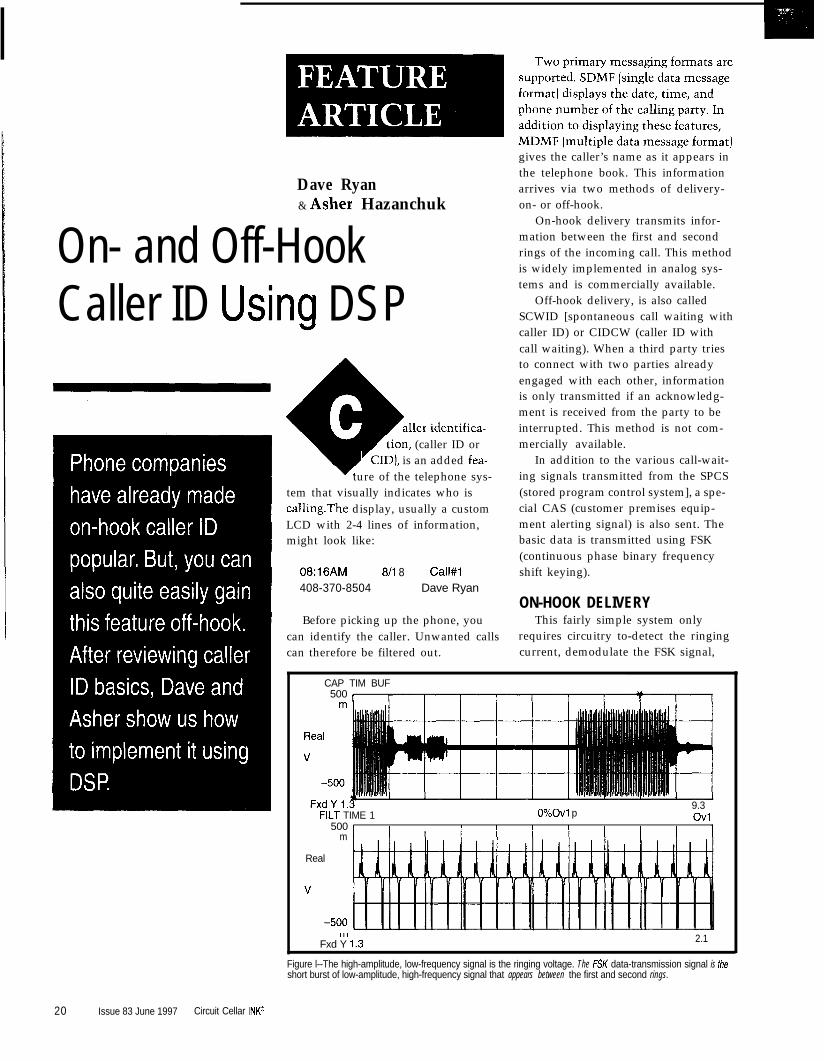
On-hook delivery transmits infor-mation between the first and secondrings of the incoming call. This methodis widely implemented in analog sys-tems and is commercially available.
Off-hook delivery, is also calledSCWID [spontaneous call waiting withcaller ID) or CIDCW (caller ID withcall waiting). When a third party triesto connect with two parties alreadyengaged with each other, informationis only transmitted if an acknowledg-ment is received from the party to beinterrupted. This method is not com-mercially available.
In addition to the various call-wait-ing signals transmitted from the SPCS(stored program control system], a spe-cial CAS (customer premises equip-ment alerting signal) is also sent. Thebasic data is transmitted using FSK(continuous phase binary frequencyshift keying).
ON-HOOK DELIVERY
current, demodulate the FSK signal,
This fairly simple system onlyrequires circuitry to-detect the ringing
CAP TIM BUF500 ,
FILT TIME 1 O%Ovl p9.3
500 IOvl
, I I I I Im
Real
III
Fxd Y 1.3 2.1
Figure l--The high-amplitude, low-frequency signal is the ringing voltage. The FSK data-transmission signal is theshort burst of low-amplitude, high-frequency signal that appears between the first and second rings.
20 Issue 83 June 1997 Circuit Cellar INK@

0 5 0 0 1000 1 5 0 0 2 0 0 0 2 5 0 0 3 0 0 0 3 5 0 0
Example data shown above is 1010
b)-2.50000 ms 0.00000 ms 2.50000 ms
ure 2a. The data alternates between 1,
and display the result-ing data.
0,1, and 0. The power spectral density
Figure 1 shows thedelivery of FSK data
plot shows this signal’s frequency
sandwiched betweenthe first and second
content in the frequency domain.
rings. The larger am-plitude, lower frequen-cy waveforms at thebeginning and end ofCAP TIM BUF (Cap-tured Time Buffer) arethe ringing pulses.
FILT TIME 1 (Fil-tered Time 1) showsthe ringing pulses ingreater detail. Thesmaller amplitude,higher frequency wave-form is the FSK data.
A somewhat ideal-ized simulation of thedata is shown in Fig-
Cl. 1 = 5 0 0 . 1 mV/div offset = - 4 0 . 0 0 mVTimebase = 5OO~sldiv Delay = 0.00000 sstart = 1.99000 Ills stop 1.15000 ms DeltaT = -820.000~sV m a r k e r l = -1.000 V Vmarker2 = l.lOOV DeltaV = 2 . 1 0 0 V
Figure 2a-A Matlab simulation shows idealized FSK and ifs corresponding power spectral density inthe frequency domain. b-An actual FSK transmission caught using a storage scope shows some ofthe impairmenfs that occur in the real world (e.g., over- and undershoots).
2 0 0 0 4 0 0 0 6 0 0 0 6 0 0 0 1 0 0 0 0Power Spectral Density (Hz)
Of course, real-world data is neveras clean idealized situation. Figure 2bshows actual received data.
It’s easy to see that the amplitudesof the high and low-frequency segmentsare quite different. In addition, noise issuperimposed on the signal, mostnoticeably on the peaks and troughs.
SDMF AND MDMFAlthough SDMF displays only the
date, time, and phone number, MDMFgive the caller’s name as well. In fact,via MDMF, any ASCII data may betransmitted.
Figure 3 shows a simplified overviewof the MDMF. The channel seizure is aseries of alternating 1s and OS that areonly supplied in the on-hook case. Off-hook as, data transmission starts withthe mark signal, which is a series of 1s.
Parameter words are not limited toone message. There may be manyparameter messages, each consisting ofa parameter type, length, and word.
Just to complicate matters, optionalmark signals may be sent betweenframes. At the end of every transmis-sion is a checksum we describe indetail later. Notice that the parameter-data length can vary.
Figure 4 illustrates an on-hooksolution. An FSK band-pass filter filters
The SDMF/MDMF section removesthe start and stop bits and determines
signals, and the FSK demodulator con-
the messaging format. Data is stored in
verts the analog signal into binary data.
SRAM or displayed on the LCD.
LCDThe display is usually a small LCD
capable of showing the caller’s date,time, telephone number, and name. Itusually has enough memory to store30-99 calls.
The system is usually battery pow-ered since the time of system opera-tion is generally limited to the timebetween the first and second ring. Oncethe call is answered, the system maybe put in power-down or standby mode.
WHY DSP?Digital signal processing isn’t nec-
essary for on-hook operation. Relativelysimple and cost-contained analog solu-tions exist. DSP makes much more
sense for off-hookoperation.
The difficulty arisesin accurately detect-ing the special CAStone in the presenceof VOX. The chipmust avoid inadvert-ent detection due tothe similarity withspeech (the Talk Offproblem).
This type of systemhasn’t been widelyimplemented in ana-log solutions prima-rily because implem-enting a cost-contain-ed, manufacturable,and robust solution isdifficult.
With digital filters,the manufacturing
difficulties associated with using criti-cally matched components [e.g., resis-tors, capacitors, inductors, etc.) arelargely avoided. In addition, the solu-tion may now be made adaptive.
Variant, implementations then be-come simply a matter of software up-grades. Of course, there are tradeoffs.A/D conversion must be supportedwith its ancillary requirements, and somust D/A conversion. However, usu-ally, a DSP solution seems far superior.
BUILDING A CALLER-ID SYSTEMThe simplest way to get caller ID is
to purchase a ready-made evaluationboard complete with firmware. How-ever, it’s certainly possible to write thesoftware and build the hardware.
While building the hardware isreasonably straightforward, softwaredevelopment is a little more complex.You’ll definitely need some firmwaredevelopment tools (e.g., an emulator,assembler, linker, and debugger).
You can see the system in Figures 5and 6. The system blocks for it are:
Figure 3-Here, you see the digital data overview as well as ifs relation to fhe overall messaging or packef structure.
Circuit Cellar INK@ Issue 83 June 1997 21

l phone-line interface-includesthe transformer and compo-nents that isolate the caller-ID circuits from the line (pro-tects against damage fromthe ring high-voltage signal)and the on-/off- hook relay
ring-detect circuit-givesdigital input (R I N G_D E T
signal) to the DSP to indi- L
cate rings on the phone lineFigure 4-These are the primay software functioning blocks with their roughinterconnection. Black areas illustrate the sections relevanf fo off-hook connection.
caller-ID gain control-con-trols signal gain coming from thephone-line interface to the codecanalog input. The DSP enables thispath by the CID_CNT control sig-nal.
codec-acts as the DSP analog frontend. The codec data format is g-bitPCM p-law. The DSP controls thesampling rate by the FSl signal andserial shifts by SCLK signal. TheDSP receives serial data from RXDand transmits serial data to TXD.
hybrid-The DSP sends the CASacknowledge via the codec and thehybrid back to the phone-line inter-face. The DSP enables this path byusing the HO_CNT control signal.
The operation is relatively simple. . _._
After power is applied and the resetbutton pushed, the LCD should dis-play “ready”. Check FSK levels on TP3.The FSK signal’s amplitude should be-3 VP p when the FSK data is beingreceived between the first and secondring. Adjust R3 1, if necessary. Then,read the LCD for the information.
OFF-HOOK DATAFigure 7 shows the delivery of FSK
data in the off-hook mode.The larger amplitude, lower frequen-
cy waveforms at the beginning of CAPTIM BUF are the call-waiting and CAStones. After a gap, the FSK data is seen.
During this gap, the DSP generatsbyan ACK. This ACK is not shown, asthe DSO was connected to the receive
Comparing the on- andoff-hook sections of Figure 4,we see many differences. Inaddition to the modules usedin on-hook selection, there’sa CAS filter for the high- andlow- band portions of theCAS signal, and special CASdetector timing.
Once the CAS tone isdetected, an acknowledgmentmust be returned via a DTMF
generator. It’s also necessary to deter-mine if the system is on or off hook.
Operation in the off-hook mode isnot as simple, due to the extra com-munication involved.
Connect P2 to line 2 or a CIDCWsimulator, if available. A simulator isis mandatory for additional develop-ment , since it involves a least 3 lines.
Again, a scope TP3 to check FSKlevels. On line 2, you should hear a call-waiting tone followed by the specialCAS tone. If all is in order, the moduledetects the tone, ACK is sent, and theSPCS or simulator transmits data.
FSK DEMODULATIONA software FSK demodulation func-
tion is integrated into the DSP as youand should be possible anywhere you side. FILT TIME shows the call wait-can subscribe to caller ID. ing and CAS tone in greater detail.
xnP-L
see in Figure 4. The FSK frequenciesare 12OOk12 and 2200+22 Hz. After all
the protocol and hand-shaking complete, thedata is sent using FSK.
This means thereare no phase discon-tinuities and only twofrequencies involvedin the FSK signal. Thelower frequency1200 Hz represents amark (logic l), and thehigher 2200 Hz repre-
I FS, sents a space (logic 0).There is no parity
or error checkingbeyond checking achecksum sent at theend of transmission. Astart bit (0) and a stop
Fi ure 5-The hardware connections of theD8P, AFE (Analog Front End), and lineinterfaces are shown.
bit (1) added to eachg-bit transmittedword.
The transmissionrate is 1200 bps anddemodulation is simi-
22 Issue 83 June 1997 Circuit Cellar INK@
lar to a standard low baud-rate V.211Bell 103 modem.
DATA RECOVERYAfter FSK demodulation, the obvi-
ous concerns are the data format (seeTable 1) and how to decode it.
The message type is 80% (128 orMDMF). Data therefore sent as param-eter words where the parameter typeand length are binary and the callingname and number are ASCII.
The last word of SMDFs or MDMFsis the checksum. The checksum is the2’s complement of the module 256sum of the binary representation of allother words in the message including
message type and length as well as theparameter type and length.
Remove the start and stop bits. Toobtain the 2’s complement, XOR with%FF. If you use Table 1 and hex calcu-lations, the checksum is:
CS = XOR (MOD(sum(80,27,01,08,~., 20, 52,79,61,6E),1001, FF)
CS = XOR (MOD(7A8, 100). FF)CS = XOR (A8, FF)CS = %57
In a practical application, the calcula-tion is less cumbersome due to thenatural modulo 256 nature of a byte.
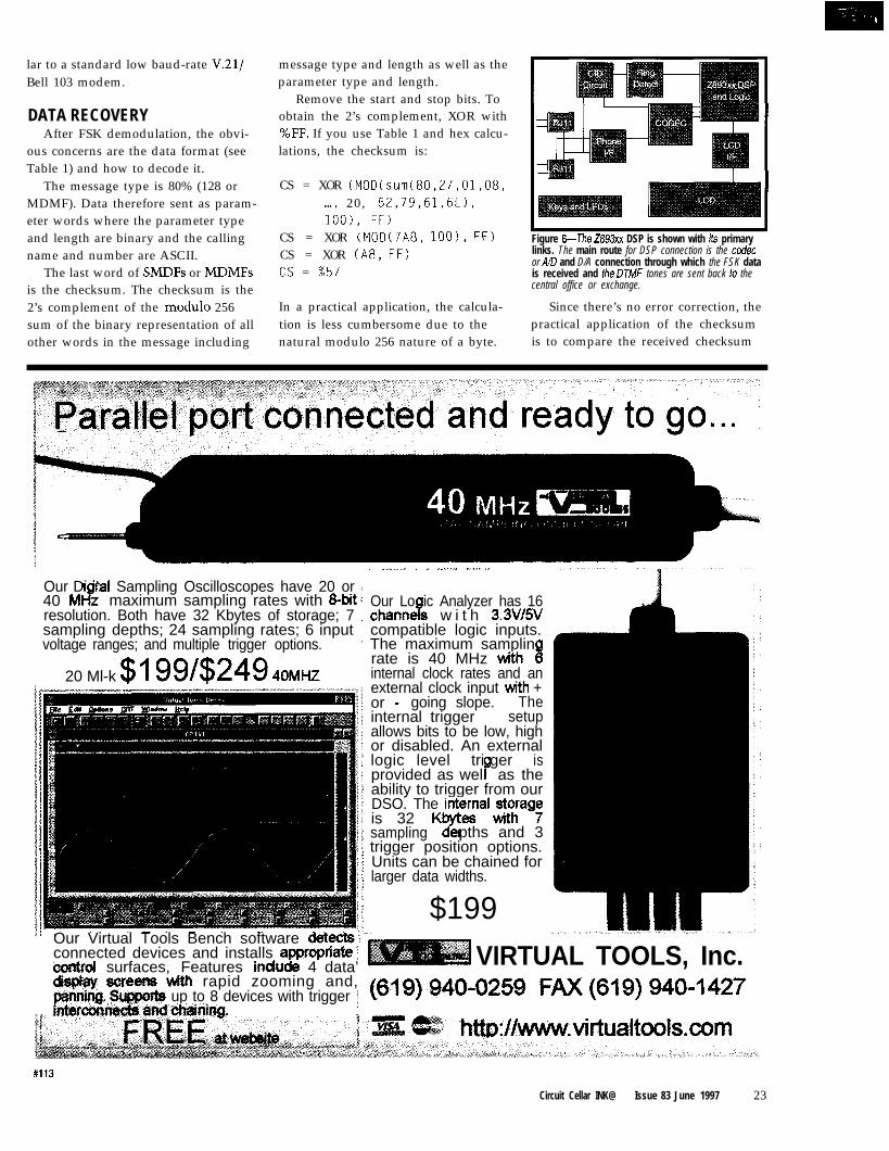
Figure GTbe Z693xx DSP is shown with its primarylinks. The main route for DSP connection is the codecor A/D and D/A connection through which the FSK datais received and the DTMF tones are sent back lo thecentral office or exchange.
Since there’s no error correction, thepractical application of the checksumis to compare the received checksum
Our Di ital Sampling Oscilloscopes have 20 or 140 Ml% maximum sampling rates with &bit :resolution. Both have 32 Kbytes of storage; 7 1sampling depths; 24 sampling rates; 6 inputvoltage ranges; and multiple trigger options. +
20 Ml-k $ ‘199/$249 4OMHZ
,~ ,.,.. . . ..,, _,,”
Our Lo ic Analyzer has 16channes w i t h 3.3Vl5VBcompatible logic inputs.The maximum samplinrate is 40 MHz with Elinternal clock rates and anexternal clock input with +or - going slope. Theinternal trigger setupallows bits to be low, highor disabled. An externallogic level tri ger isprovided as welB as theability to trigger from ourDSO. The inteFl$r$is 32sampling K!Ytepths and 3trigger position options.Units can be chained forlarger data widths.
$199Our Virtual Tools Bench software detects: *.connected devices and installs appropriatesccntrcl surfaces, Features indude 4 data’ VIRTUAL TOOLS, Inc.dkqdq mm v&h rapid zooming and,pan&g. Suppc& up to 8 devices with trigger ; (619)940-0259 FAX(619)940-1427t~~~~~~~~~n~
Circuit Cellar INK@ Issue 83 June 1997 23
with the calculated one. If they don’tagree, then the data is bad and shouldgenerally not be displayed.
CAP TIM BUF Ovl1313 r I I II
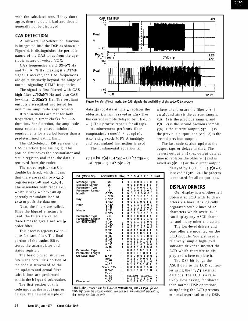
CAS DETECTIONA software CAS-detection function
is integrated into the DSP as shown inFigure 4. It distinguishes the periodicnature of the CAS tones from the ape-riodic nature of voiced VOX.
SC
FxdY 0 . 0FILT TIME 1
160
I I I I I I IO%Ovl p
i .2aOvl
CAS frequencies are 2130+5% Hzand 275Ok5 % Hz, making it a DTMFsignal. However, the CAS frequenciesare quite distinctly beyond the range ofnormal signaling DTMF frequencies.
The signal is first filtered with CAShigh-filter 2750+5% Hz and also CASlow-filter 2130*5% Hz. The resultantoutputs are rectified and tested forminimum amplitude requirements.
Figure 7-/n the off-hook mode, the CAS signals the availability of fhe caller-/D infomation.
If requirements are met for bothfrequencies, a timer checks for CASduration. For detection, the amplitudemust constantly exceed minimumrequirements for a period longer than apredetermined gating limit.
The CAS-detector ISR services theCAS detection (see Listing 1). Thisportion first saves the accumulator andstatus register, and then, the data isretrieved from the codec.
data x(n) or data at time n replaces the where bi and ai are the filter coeffi-older x(n), which is saved as x(n - 1) or cients and x(n) is the current sample.the current sample delayed by 1 (i.e., n x(n - 1) is the previous sample, and_ 1). This process repeats for all taps. x(n - 2) is the second previous sample.
Autoincrement performs filter y(n) is the current output, y(n - 1) iscomputations (coeff * sample). the previous output, and y(n - 2) is theAlso, a single-cycle M PY A (multiply second previous output.and accumulate) instruction is used. The last code section updates the
The fundamental equation is: output taps or delays in time. Thenewest output y(n) (i.e., output data at
y(n) = bO*x(n) + Bl*x(n - 1) + b2*x(n - 2) time n) replaces the older y(n) and is+a1 *y(n - 1) + a2*y(n - 2) saved as y(n - 1) or the current output
The codec register ext6 isdouble buffered, which meansthat there are really two ext6registers-extb-0 and extb-1.The assembler only reads ext6,which is why we have an ap-parently redundant load ofext6 to push the data out.
Next, the filters are called.Since the biquad structure isused, the filters are calledthree times to give a net sixth-order filter.
This process repeats twice-once for each filter. The finalportion of the casint ISR re-stores the accumulator andstatus register.
The basic biquad structurefilters the core. This portion ofthe code is structured so thetap updates and actual filtercalculations are performedwithin the b i qua d subroutine.
The first section of this
Bit (MSB-LSB) ASCII/HEX% Stop 7 6 5 4 3 2 1 0 Start
Message Type I60 1 1 0 0 0 0 0 0 0 0Message Length I27 0 0 1 0 0 1 1 1 0Parameter Type /I 1 0 0 0 0 0 0 0 1 0Parameter Length 0 0 0 0 1 0 0 0 0Month 0:830 1 00110000 0
6/36 0 0 1 1 0 1 1 0 0Day 2/32 ; 0 0 1 1 0 0 1 0 0
3133 1 0 0 1 1 0 0 1 1 0Hour o/30 1 0 0 1 1 0 0 0 0 0
a/38 0 0 1 1 1 0 0 0 0Minute 1 I31 1 0 0 1 1 0 0 0 1 0
6/36 0 0 1 1 0 1 1 0 0Parameter Type I3 ; 0 0 0 0 0 0 1 1 0Parameter Length / A 0 0 0 0 1 0 1 0 0DN 4083708504 4134 1 0 0 1 1 0 1 0 0 0
o/30 1 0 0 1 1 0 0 0 0 0a/38 0 0 1 1 1 0 0 0 03133
10 0 1 1 0 0 1 1 0
7137 0 0 1 1 0 1 1 1 0o/30
;0 0 1 1 0 0 0 0 0
81385/35
; 0 0 1 1 1 0 0 0 00 0 1 1 0 1 0 1 0
o/30;
0 0 1 1 0 0 0 0 04134 0 0 1 1 0 1 0 0 0
Parameter Type ;: 1 0 0 0 0 0 1 1 1 0Parameter Length 0 0 0 0 1 0 0 1 0CN Dave Ryan D/44 1 0 1 0 0 0 1 0 0 0
a/61v/76
; 0 1 1 0 0 0 0 1 00 1 1 1 0 1 1 0 0
e / 6 5 1 0 1 1 0 0 1 0 1 0Space /20 1 0 0 1 0 0 0 0 0 0
RI52 1 0 1 0 1 0 0 1 0 0
ya:z 1 01111001 01100001 0 0lll6E 0 1 1 0 1 1 1 0 0
Checksum I57 i 0 1 0 1 0 1 1 1 0
12am
code updates the input taps or Table l--This traces a call by Dave at 0816 AM on June 23. lfyou follow
delays. The newest sample ofvertically down the second column, you can see the individual elements ofthis transaction byfe by byte.
delayed by 1 (i.e., n - 1). y(n - 1)is saved as y(n - 2). The processis repeated for all output taps.
DISPLAY DRIVERSOur display is a off-the-shelf
dot-matrix LCD with 16 char-acters x 4 lines. It is logicallyorganized with 2 lines of 32characters which overrun. Itcan display any ASCII charac-ter and many other characters.
The low-level drivers andcontroller are mounted on theLCD module. You just need arelatively simple high-levelsoftware driver to instruct theLCD which character to dis-play and where to place it.
The DSP bit bangs theASCII data to the LCD control-ler using the DSP’s externaldata bus. The LCD is a rela-tively slow device, far slowerthan normal DSP operations,so updating the LCD presentsminimal overhead to the DSP.
24 Issue 83 June 1997 Circuit Cellar INK@

Listing l--The base filter’s b i qua d roufine may be used for a great variety of filters. Of course, the filtercoefficients must be computedin each case. Note the single-instruction mulfiplyandaccumulafe capability.
; Fl Sixth-order triple biquad IIR filterId a ,#Xll ;load Act with address (X11) for input samplesId pO:O,a ;point to input sampleId a ,#BFl :address (BFl) for filter coefficientsId pO:l,a ;point to filter coefficients
;read new input sample x(n)Id ext6.a ;push new ulaw input sample ext6-2 to ext6-1Id a,ext6 ;load u-law data to accumulator x(n)Ulaw :u-law result is 14.bit sign magnitude numbersll a ;shift left logical, multiply by 2sll a :shift left logical, multiply by 2Id x,a ;x = new dataId tempist,a :store temporary input storagecall biquad ;perform standard biquadcall biquad ;perform standard biquadcall biquad ;perform standard biquad
; save output filter response y(n)Id outgbf1.a ;store third-stage output
; Id ext6,a ;Codecl output y(n) auto hardware u-lawendinti:
ret ;return from Codec ISRbiquad:
;perform filter computations (coeff * sample) using autoincrement;y = bO*X(n) + Bl*X(n-1) + b2*X(n-2) +al*Y(nl) + a2*Y(n-2);Input New Sample is in x, Output is in Act: update input sample buffer
Id y,@pO:O ;y saves old (n) pO:O points at (n)Id @pO:O+,x ;(n) = new sample pO:O points at (n)Id x,@pO:O ;x saves old (n-1) pO:O points at (n-1)Id @pO:O+,y ;(n-1) = (n)Id y,@pO:O ;y saves old (n-2) pO:O points at (n-2)Id @pO:O,x ;(nZ) = (n-1)id a,pO:O ;pO:O points at (n-2)sub a,#%2 ;decrement actId pO:O,a ;pO:O points at (n)
;y ;,tO*X(n) + Bl*X(n-1) + b2*X(n-2) +al*Y(nl) + a2*Y(n-2)@pO:l+,@pO:O+,on ;A= 0 P = (b0 * X11) X11 = X(n)
mpya @pO:l+,@pO:O+,on ;bl * X12 Xl2 = X(n1)mpya @pO:l+,@pO:O+,on ;b2 * Xl3 Xl3 = X(n-2)mpya @pO:l+,@pO:O+,on ;a1 * Yll Yll = Y(n-1)mpya @pO:l+,@pO:O+,on ;a2 * Y12 Y12 = Y(n-2)add a,p :add result of last multiply to Act.sll a ;scale back if divide by 2 on coefficientsId x,a ;return result in x
;update output bufferId a,pO:O ;pO:O points at YlZ+lsub a,#%2 ;decrement actId pO:O,a ;pO:O points at Yll (n-1)Id y,@pO:O ;y saves old (n-1)Id @pO:O+,x ;Yll = new resultId @pO:O+,y ;YlZ = Yll = Y(n2)
; output filter response y(n)Id a,x ;store stage outputret :return from biquads
Communication is done via a spe- When the SDMF or MDMF data iscialized series of LCD instructions. received, it should be displayed. AOnce the LCD is initialized, the data is state machine takes care of the logicaltransmitted. progress of the call. At the end of the
call, a disconnection occurs and theCALL PROGRESS entire cycle repeats.
Call progress is sequential. A ringmust be detected first. Once the call is MEMORY STORAGEestablished, only one of two events can Again, due to the multitaskinghappen-either a call interrupt occurs features common to DSPs, normal callor does not occur. progress, especially on-/off-hook moni-
toring, system supervision, memoryfor calls received, and display tasks,can be handled by a single DSP.
For the sake of simplicity, we didn’tadd memory storage to this demo. Theexternal bus addressing capabilityenables this feature to be easily added.
TAKE IT FURTHERThe system described is elemental.
Many value-added features are possible(e.g., ring only on certain callers). Suchfeatures are easily added as controllerfunctions.
Just let your imagination lead.. qDave Ryan is a systems engineer inZilog’s data communications. Heworks on their next-generation 50-MIPSfixed-point processor-class device. Youmay reach Dave at [email protected].
Asher Hazanchuk works in SDP sys-tem engineering and applications atZilog. He has 15 years of DSP experi-ence in image processing and com-pression, digital answering machines,cell phones, caller ID, magnetic-stripereaders, and DSP architectures.
The complete code for this article isavailable on the Circuit Cellar Website.
J.D. Gibson, Principles of Digitaland Analog Communications,MacMillan, New York, NY, 1993.
Bellcore, Technical Reference TR-NWT-000031 and NWT-001188.
Bellcore, Generic Requirements GR-30-CORE.
Bellcore, Special Reports SR-TSV-002578 and SR-TSV-002476.
Z89CIDOOZCOZilog2 10 Hacienda Ave.Campbell, CA 95008-6600(408) 370-8000Fax: (408) 370-8056
404 Very Useful405 Moderately Useful406 Not Useful
Circuit Cellar INK@ lssue83June1997 2 5
Chris Sakkas
PC Telephone Interface
’ duce fascinating applica-tions beyond simple voice mail. Com-puter telephony also includes completeinteractive voice-response systems, callprocessing, autoattendants, and more.
As well, computer telephony integra-tion can lead to interesting applicationsinvolving remote access to computercontrol and home-automation systems.
In this project, a low-cost ISA expan-sion card serves as a complete tele-phone interface. It records and playsback messages, decodes touchtones,dials, and handles switch-hook control.
I also discuss software for develop-ing a nine-mailbox voice-mail system.This software-hardware combinationis a useful base for creating applicationsfor voice messaging, call processing,home automation, and more.
CONCEPTFigure 1 outlines the hardware de-
sign, showing the telephone input tothe card as well as the I/O and func-tional relationship of individual items.
The Data Access Arrangement takestelephone input and passes it to a sum-ming amplifier to mix the signal withthe microphone input. This input isamplified to a level ready to sample viathe preamplifier and a second amplifier.
The signal is fed through the anti-aliasing low-pass filter and sampled bythe ADC. Since the phone systembandwidth is limited to -4 kHz, thesampling frequency must be at least8 kHz to satisfy the Nyquist sampling-frequency theorem. The CPU gets thisdata byte via the ISA interface.
After the DAC converts PC data toanalog form, the signal is fed into areconstruction filter and then mixedwith the DTMF transmitter output.An audio amplifier amplifies the signalinto levels capable of driving a speaker.
SPECIFICATIONSThe hardware needed to handle
8-bit A/D and D/A conversions, aswell as DTMF tone decoding and trans-mission. It had to be able to sample a4-kHz signal, and its data storage ratewas limited to at most 8 kbps.
Figure l--The input and output relationship of all subsystems is shown. Many of the subsystems were implementedin sing/e monolithic devices.
26 Issue 83 June 1997 Circuit Cellar INK@
As well, it needed an RJ-11 phone-line connection and a user-selectableport address. Finally, it had to satisfyFCC Part 68 requirements.
To minimize components, com-plexity, and cost and maximize thehardware’s flexibility, I chose highlyintegrated components to handle theinterface logic, A/D and D/A conver-sions, DTMF decoding and transmis-sion, and telephone-line interfacing.
HARDWARE
The Xecom XE0068 Data AccessArrangement provides TTL-level ringdetection and switch-hook control.The internal Automatic Gain Control(AGC) circuit optimizes transmit lev-
The 74LS244 also buffers betweenthe bus and hardware, the I/O read andwrite lines, and the two least signifi-cant bits of the address bus. These bitsThe Analog Devices AD7569 g-bit
Analog I/O system provides fast A/D els and maintains a small package size. are needed for decoding which of .theand D/A conversion in a small, low- This device provides a legal, low- four port addresses is to be used forcost 24-pin package. It has a minimal cost interface to the phone system with hardware access.
bus interface, 2-ps conversion time,and single supply voltage, which ac-cepts several ranges of input voltages.
The Teltone M-8888 DTMF trans-ceiver handles DTMF tone decodingand transmission. This 20-pin packageprovides easy interfacing with a micro-processor and has a call-progress mode.(It works with a single supply voltage.)
its FCC Part 68 registration. The regis-tration transfers to the end application.
Figure 2 shows the schematic forthe interface card. A 74LS688 8-bitcomparator is used as a decoder for theboard. When an address correspondingto the card’s base port address is de-tected, the enable of the 74LS245 octalbus transceiver is selected so the data-bus contents can be accessed.
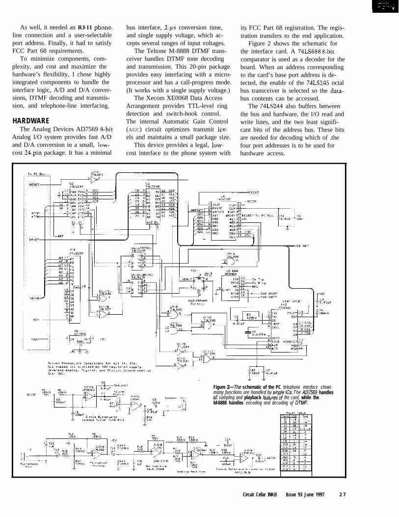
Figure 2-The schematic of the PC telephone interface showsmany functions are handled by single Es. The ADi‘569 handlesall sampling and playback feaiureiof the card, while theM-8888 handles encoding and decoding of DTMF
Circuit Cellar INK@ Issue 93 June 1997 2 7

R A T I O N
S.P.D.T. snap-action switch withroller positioned above switchactuator. Rated 5 amps Q125/250 vat. Switch body: 1 .I”x 0.63” x 0.375”. Solder or qcterminals. UL and CSA listed.
CAT# SMS-1 ii
b,
Nichicon LGQ2W471 MHSC1.375” diameter x 2” high.0.4” lead spacing.
CAT# EC-4745
94%!h
Semi-circular, irregularly-shaped magnets.Shiny finish with a polarity marking dot.0.93” long x 0.3” x 0.07” thick.Powerful for their size.
CAT# MAG-30
I160 PCS. - $100.00 1
Enertron# NX586-022-207 blade, mini 12 vctcfan -on a heatsink.Assembly is 2”sauare X 1.22n
a 0.87” square flatarea on side opposite fanfrom which fins radiate. One finextends 0.63” beyond the others. Includestwo mounting clips.
CAT # CF-40 @!h
TERMS: NO MINIMUM ORDER Shippmg and handlhg for theIS continental U.S.A. $5 00 per order. All others including AK,HI. PR or Canada must pay lull shipping. All orders deliveredn CALIFORNIA must include local state sales tax. Quantities
CALL, WRITELimlted NO COD Prices subjectto chanoe
FAX or E-MAILfor our FREE
-7
without
96 PageCATALOG
Outside the U.S.A.send $3.00 P’=tWe.
#114
Port Bit Read Write
$300 0 Ring detect (0 = ring) Hook switch (0 = on, 1 = off)$301 O-7 ADC read DAC write$302 O-3 Read DTMF receiver Write to DTMF transmitter$303 O-3 Read DTMF status register bit Write DTMF control register
! l-Four PC I/O sorts are used for the card. Additional functionality can be added to the card and controled viathe first port address if’needed.
The 74LS139 consists of two 2-to-4decoders, each supplied with A0 andAl of the address bus. The appropriateportion for reading or writing is en-abled, depending on the status of the*IOR and ‘IOW bus lines.
The base address of $300 (hex) isused, but any nonconflicting address ispossible. Changing the address meanspins 16 and 18 of the 74LS688 shouldbe tied high. The rest should be low forthis addressing example. Table 1 liststhe port addresses and functions.
Depending on the action taken bythe 74LSI39, the appropriate compo-nent is enabled-either the AD7569for read or write or the M-8888 forread, write, or register selection.
It can also read the contents of theXE0068’s Ring Indicator pin via thesecond half of the 74LS244. Or, it cantoggle the hook switch by changingthe contents of the 74LS744 D-typeflip-flop [which acts as a I-bit register).
The AD7569 converts data whenit’s selected and the l RD (read) pin isstrobed. The IC activates its *BUSYline, which is connected to ‘IORDYon the PC bus. This action extends theread’s bus cycle if necessary to theamount needed for a read to occur.
Due to the relatively low samplingfrequency, I didn’t use precise timingcircuitry. All timing was done via thePC’s programmable interval timer.
In a PC-compatible system, thistimer has three different channels, andchannel zero is the system clock-ticktimer. The ROM BIOS programs thetimer to generate an interrupt 08 at afrequency of 18.2 times per second.
For most systems, however, thisfrequency can be reprogrammed tooccur at a much greater rate, making itmore useful for this project. Softwarecan reprogram the timer and still main-tain the proper call to other serviceroutines 18.2 times per second.
I chose a microphone preamplifierbased on a noninverting amplifier
using one-half of a TL082 operationalamplifier. The op-amp is biased tooperate from a single 5-V supply, as areall other op-amps in this design.
The preamp provides a 20-dB gain.This low-level signal is amplified againby the second-half of the TL082 op-ampconfigured as another noninvertingamplifier with a gain of 23.5 dB.
I chose National Semiconductor’sTL082 JFET input operational ampli-fier for its high input impedance, lownoise voltage, and low input bias cur-rent. These features make it ideal forconverting a microvolt signal to amillivolt signal.
A summing amplifier mixes out-puts from the microphone amplifica-tion circuitry and the DAA’s receiver,using one-fourth of an LM324 op-amp.The summing amplifier’s output isapplied to a two-pole Butterworth low-pass filter before entering the ADC.
A second summing amplifier mixesthe DAC and DTMF outputs. A two-pole Butter-worth low-pass filter acts asa reconstruction filter for this signal.
Both filters in this design are identi-cal and are based on the popular unity-gain Sallen and Key configuration. Iuse National Semiconductor’s LM324quad op-amp for both since it is lowcost and has four op-amps per package.The filters were designed for a 3.4.kHzcut-off frequency, appropriate for filter-ing out aliasing signal elements forthis application.
The reconstruction filter output isapplied to the DAA’s transmit pin andthe input of the LM386 audio ampli-fier. The LM386 amplifier providesadequate audio amplification in a low-cost monolithic package. The audiooutput connects to a jack on the backof the card.
SOFTWAREVoice data is managed by a message
structure, mess-t (see Web site forsource code). It stores a pointer to the
28 Issue 83 June 1997 Circuit Cellar INK@

actual voice message data, the numberof data bytes, an indicator of whetherthe data is in memory or stored on disk,a message description, and a filename.
An enumerated type, b i t-s t a t us,is defined with on and off for Booleancontrol. The software has functionsthat can be integrated into other pro-grams to incorporate telephone sup-port. The routines are divided intotelephone-control, message record andplayback, and DTMF functions.
Telephone-control functions in-cludeWaitForRing,HookSwitch,and RingDetect.WaitForRing waitsfor an incoming number of rings basedon the variable co LI n t Control goes tothe calling function after the specifiedring number is encountered.
HookSwi tch simply controls thetelephone’s hook-switch status, eitheron or off. Ri ngDetect returns on if aring is detected and off otherwise.
Read F i 1 e, a message record andplay-back function, reads a specifiedfilename into memory for playback.Play-MessageandRecordMessageexpect a me s s_t structure to be passedto begin playback or recording. ThePC’s programmable interval timer isused for machine-independent timing.
DTMF initialization is performedvia DTMFInit.DTMFReceive andDTMFTransmi t read or place the DTMFcharacter in the M-8888 buffer. DTMF -Transmit mustbesetupwithacalltothe DTMFToneBurst function.
With these functions, I developed asmall voice-mail application for ninemailboxes. After a main greeting andthe individual voice message for eachmailbox is played, the user may recorda message at the tone.
The main greeting is contained inthe file G R E ET - MN. Mailbox greetingsare contained in G R E ET x, where xdenotes the mailbox number. A re-ceived message is stored in M ES G E - x.This entire application was coded in-60 lines of C code.
Several example programs showfurther potential uses of the card. Theseprograms can record to a file, playbacka file, and act as a telephone dialer.
INTERFACING IDEASThe PC-telephone interface pro-
vides an easy way to interface a PC-
compatible computer to the telephonenetwork. Other more sophisticatedapplications can be developed, includ-ing many beyond typical computer-telephony applications.
A home-automation or other com-puter-controlled system can be modi-fied to receive commands and deliverreports remotely. With added circuitry,a complete amateur-radio repeatercontroller can be created with voiceand sophisticated computer control. q
Chris Sakkas is president of ITU Tech-nologies, a company specializing indevelopment tools for microcontrol-lers. You may reach him via E-mail [email protected] or by telephone at(513) 574-7523.
The complete source code for thisarticle can be downloaded from theCircuit Cellar Web site.
AD7569Analog DevicesOne Technology WayNorwood, MA 02062-9 106(617) 329-4700Fax: (617) 329-1241
M-8888Teltone Corp.22121 20th Ave. SEBothell, WA 98021(206) 487-1515Fax: (206) 487-2288
XE0068Xecom374 Turquoise St.Milpitas, CA 95035(408) 9456640Fax: (408) 942- 1346
TL082, LM324, LM386National SemiconductorP.O. Box 58090Santa Clara, CA 95052-8090(408) 721-5000Fax: (408) 739-9803
407 Very Useful408 Moderately Useful409 Not Useful
Jse Your PC Development ToolsNo MORE CRASH & BURN EPROM
Technology
DOS Single Board Computerwith 572 k FLASH Memory disk drivei 10 Mhz/8 Mhz CPU Sr 2 Timersd 512 k bytes RAM ab’ 4 Interrupt Lines/ 512 k/256 k FLASH v* 8 Analog InputsP 2 Serial Ports ti X-Modem File/’ 24 Parallel l/O Lines Transfer
INCLUDES DOS & Utilities
J 8 Channels, 12&sJ 6 ps. Conversion Timeu’ ClockfCalendar Option
Includes Drivers & Apps.
4 8 Opto-Isolated Inputs
JK micros stemsCost Effective YControl ers for hdustry
TO ORDER (510) 2364151FAX (510) 236.2999-email: [email protected] our WEB site-www.dsp.com/jkmicra1275 Yuba Ave., San Pablo, CA 94806
Circuit Cellar INK@ Issue83 June1997 29

Art Sobel
Embedding the ARM7500Part 2: Programming anEmbedded Computer
0 he ARM7500 isexceedingly compli-
cated, having similarresources to a typical PC’s
CPU and motherboard logic. Afterbuilding the development board, myfirst task was porting the C-Demon, aROM-based monitor used in otherARM development boards.
Demon initializes the ARM andperipheral registers, builds a compatiblememory map for monitor variables, andstarts communication with the host.
After the C-Demon was working,each major chip section needed drivers.These drivers are wrapped up in theconsole test program.
The ARM7500’s ROM controllerresets to 16-bit mode. I chose a 32-bit-wide ROM for the onboard software.This switch was a bit tricky as theARM program counter nearly alwaysfetches two instructions ahead of theexecution unit.
The ARM7500’s CPU and MEMCmemory, I/O, and VIDC video/soundcontrollers were conserved from theoriginal Acorn computer, keeping theoriginal OS and user software some-what compatible.
From a programmer’s view, theARM7500 functional blocks areseparate sets of registers incorpo-rated in the memory map asshown in Figure 1.
In 16.bit mode, the memory control-ler accesses the low and then the high16 bits and presents the assembled32-bit word to the instruction unit. InListing 1 (Level 0 code), the first 14entries have the upper 16 bits zeroed.
The ROM start-up code is handassembled since the rest of the code is
ARM704
4.KB Cache
As Table 1 shows, the IOChandles internal peripherals likekeyboard and mouse control, 11general-purpose I/O pins, videoflyback, and two 16.bit timers. It
Figure l-Acorn’s former discrete chipsef,CPU, /OC, MEMC, and V/DC are preserved inthe layout of the ARM7500.
also controls six sets of interrupt-con-trol registers, four single-slope ADCsfor the joystick interface, memory andI/O timing, as well as ROM and DRAMwidth.
Lastly, the IOC has registers control-ling the clocks. The CPU clock can beturned off, or the whole chip can haveclocks suspended.
The external clock can also be con-trolled. In stopped mode, an externalclock/calendar restarts the chip bygrounding one of two special interruptpins.
The DMA channels were histori-cally part of the MEMC. The basicDMA channels are retained in theARM7500 (see Table 2).
The myriad video-timing registers,pixel control, and clock control, aswell as the analog sound clock andsteering register are placed in the VIDCfunctional block (see Table 3).
C-DEMON PORTING
Clock Control
30 Issue 83 June 1997 Circuit Cellar INK@

Name Address Size Read Write Descripbon Name Address Size Read Write
IOCR 00 8 IOCR IOCR I/O Pin Ctrl VIDCAUX 6C 8 VIDAUX VIDAUXKBDAT 04 8 KBDATIN KBDATOUT Keyboard Data IRQSTD 70 8 IRQ StatusD -KBDCR 08 8 KBDCR KBDCR Keyboard Stat and Ctrl IRQRQD 74 8 IRQReqD -IOPINS o c - IOPINS IOPINEN 8 Open-Drain l/O Pins IRQMSKD 78 8 IRQ MaskD IRQ MaskDIRQSTA 10 8 IRQ StatusA - IRQA Stat ROMCRO 80 8 ROM&n0 ROMConOIRQRQA 14 8 IRQ ReqA IRQ clear A IRQA Req ROMCRl 84 8 ROMCon 1 ROM Con 1IRQMSKA 18 8 IRQ MaskA IRQ MaskA IRQA Mask RESV 88 8-IDLEMD 1c l- Enter IDLE MODE CPU Idle Cmd RFSHCR EC 8 Refresh CR Refresh CRIRQSTB 20 8 IRQStatusB - IRQB Stat ID0 94 8 Chip ID L byte -IRQRQB 24 8 IRQ ReqB - IRQB Req ID1 98 8 Chip ID H byte-IRQMSKB 28 8 IRQMaSKB IRQMaskB IRQB Mask VERSION 9c 8 Chip VersionSTOPMD 2c l- Enter STOP MODE Clock Stop Cmd MSDAT A8 8 MSDATIN MSDATOUTFIQST 30 8 FIQ Status - FIQ Stat MSCR AC 8 MSCR MSCRFIQRQ 34 8 FIQ Req - FIQ Req reserved BC!-BCFIQMSK 38 8 FIQMaSK FIQ Mask FIQ Mask IOTCR c 4 8 IOTiming IO TimingCLKCTL 3C 8 CLKCTL CLKCTL Clock Ctrl ECTCR C8 8 Ext IO Timing Exl IO TimingTOLOW 40 8 TOcountL TOLatchL Tmr 0 Latch Data Low ASTCR c c 8 ASTCR ASTCRTOHIGH 44 8 TOcountH TOLatchH Tmr 0 Latch Data High DRAMWID D O 8 DRAMWID DRAMWIDTOGO 48 O- TOGO Command Tmr 0 Start SELFREF D4 8 SELFREF SELFREFTOLAT 4c o- TOLatch Tmr 0 Latch Cmd JOYICR E O 8 JOYICR JOYICRTl LOW 50 8 TlcountL Tl LatchL Tmr 1 Latch Data Low JOYSR E4 8 JOYSR -TlHlGH 54 8 Tl CountH Tl LatchH Tmr 1 Latch Data High JOYCC E8 8 JOYCC JOYCCTlGO 58 O- TlGo Tmr 1 Start JOYCNTO EC 1 6 J O Y C N T O -Tl LAT 5c o- Tl Latch Tmr 1 Latch Cmd JOYlCRl FO 16 JOYlCRl -IRQSTC 60 8 IRQ StatusC - IRQC Stat JOYICRP F4 16 JOYICRP -IRQRQC 64 8 IRQReqC - IRQC Req JOYICRB FE 16 JOYICRB -IRQMSKC 68 8 IRQ MaskC IRQ MaskC IRQC Mask reserved FC-17C
Description
Video Aux CtrlIRQD StatIRQD ReqIRQD MaskROM 0 Timing CtrlROM 1 Timing Ctrl
DRAM Refresh Ctrl
Mouse DataMouse Ctrl and Stat
IO Timing CtrlEASICS TimingExt MEMC TimingDRAM WidthSelf Refresh CtdJoystick Int CtrlJoystick StatJ o y s t i c k CtrlJoystick Ctrl 0Joystick Ctrl 1Joystick Ctrl 2Joystick Ctrl 3
Table l--The I/O confrolprocessor registers manage the keyboard, mouse, interrupts, timer, joystick, and memory-control functions.
in normal 32-bit format. The code loads After RAM size is found and the stacks a protected-mode ‘x86 processor withan immediate value for the internal I/O for the various ARM operation modes all its hardware interrupt-assist logic.controller address and the new ROM-controller value, and then loads it intothe ROM controller.
are initialized, the cache is enabled.
After this code, the PC is directlyloaded with 0. Although the ROMcontroller s t 0 r e instruction is writtenbefore the jump, it executes afterwards.The start-up code is reinterpreted in32-bit mode as a series of NOPs.
The next task is programming theinternal registers for the interrupts,timer, and other functions (see Table 1).
The interrupts differ greatly fromthe previous ARM600 PID port. TheARM7500 has five IRQ (normal inter-rupt) and one FIQ (fast interrupt) regis-ters. Thus, the processor reads up tofive 8-bit registers to find out whichinterrupt caused an IRQ and one 8-bitregister to locate the FIQ source. Eachinterrupt request register is read andeach bit is examined for the first set bit.
The ARM7500 has two 16-bit timersoperating at 2 MHz (with a 32-MHz I/Oclock). To produce an -lOO-Hz continu-ous interrupt every 10 ms, the 2 MHzis divided by 20,000.
Communications with the host areaccomplished via the serial port on thePC I/O Combo chip (FDC37C665) orEthernet (SMC91C94).
The next trick is to remap the mem-ory using the MMU (see Table 4). I tookadvantage of the ROM being mappedto 0 and also mapped to 0x20000000,since the physical memory map repeatson 512-MB boundaries.
The I/O Combo’s serial port is16C550 compatible, so the code usedin the previous PID board works but ata different address.
The program jumps to the higherROM location and initializes the MMUpage-table pointer to a precalculatedprimary page table at the endof ROM. The cache remainsoff so the RAM size may bedetermined.
This bit’s location indexes into atable of interrupt routines. Despite suchcomplexities, the ARM7500 can handlethe interrupt routine much faster than
The next steps to start the Demonare common to all versions. You set updata structures in low-memory RAM,check ROM for the correct checksum,and send a banner message to the host.
Since the actual RAM issmaller than the huge spaceallotted (64 MB in each bank),the physical RAM repeatsseveral times. The RAM sizeis found by detecting therollover to RAM address 0when its size is exceeded.
When cache is enabled,figuring out RAM size be-comes a problem. The cachetag thinks address 0 is stillvalid even though it’s over-written from a higher address.
Name Address Size Read Write Description
SDOCURA 180 32 SD0 0 Current A SD0 0 Current A Ch A CurrentSDOENDA 184 32 SD0 0 End A SD0 0 End A Ch A EndSDOCURB 168 32 SD0 0 Current B SD0 0 Current B Ch B Current
SDOENDB 18C 32 SD0 0 End B SD0 0 End B Ch B EndSDOCR 190 8 SD0 0 Control SD0 0 Control Sound ControlSDOST 194 8 SD0 0 Status Sound Status
CURSCUR 1co 32 Curs Current curs current
CURSINIT lC4 32 Curs lnit Curs lnit
VIDCURB lC8 32 VIDEO Current VIDEO Current BVIDCURA 1DO 32 VIDEO Current VIDEO Current AVIDEND lD4 32 VIDEO End VIDEO EndVIDSTART lD8 32 VIDEO Start VIDEO StartVIDINITA 1DC 32 VIDEO INIT VIDEO INIT AVIDCR 1EO 8 VIDEO Control VIDEO ControlVIDINITB lE8 32 VIDEO INIT VIDEO INIT B
DMAST 1FO 8 DMA StatusDMARQ lF4 8 DMA IRQ Req DMA IRQ ReqDMAMSK lF8 8 DMA IRQ Mask DMA IRQ Mask
Table 2-ARM7500 DMA registers are loaded according to their state diagram inFigure 4.
CONSOLE TEST PROGRAMThe console test program
checks the functions of theRC7.500 and ARM7500, as wellas the additional onboard logic.Source code for all tests helpsyou get a feel for the softwaredrivers (see Listing 2). Whenthe console program is run,Figure 2 appears onscreen.
RAW VIDEOGetting video comes first.
Without a functional display,no progress is possible.
The ARM7500 video regis-ters are in Table 3. The display
Circuit Cellar INK@ Issue 83 June 1997 31


Register Data VGA Value Descr!ptlon Register Data VGA Value Description
VPVPAR
LOROLORIBCR
CPClCPC2CPC3HCR
HSWRHBSRHDSRHDERHCERHCSR
oxxxxxxx1 oooooxx2 x x x x x x x3oooooxx310000xx4 x x x x x x x5 x x x x x x x6XXXXXXX7 x x x x x x x8oooxxxx81ooxxxx82ooxxxx83ooxxxx84ooxxxx85ooxxxx8600XXXX87ooxxxx88ooxxxx8900XXXX8COOXXXX
800003368100002C820000728300008084000300850003248600007f
Video PalettePalette addressResewedLCD Offset Register 0LCD Offset Register 1Border ColorCursor Palette Color 1Cursor Palette Color 2Cursor Palette Color 3Horizontal Cycle RegisterHorizontal Sync Width RegisterHorzontal Border Start RegisterHorizontal Display Start RegisterHorizontal Display End RegisterHorizontal Border End RegisterHorizontal Cursor Start RegisterResewedTest RegisterResewedTest Register
VCRVSWRVBSRVDSRVDERVBERVCSRVCER
SIR[O-71 AOOOOOOX-A700000XSFR BOOOOOOXSCR Bl 00000X
EXRFSRFSRFSR
cooxxxxxDOOOXXXXEOOXXXXXFOOOXXXX
9oooxxxx 900002079100xxxx 910000039200xxxx 9200001 E9300xxxx 9300001 E9400xxxx 940001 FE9500xxxx 940002079600XXXX9700xxxx98OOXXXX-9COOXXXX
VeltlcalVelttcalVertical Border RegisterVertical Display Start RegisterVertical Display End Register
VelticalVeltical
Table3-ARM7500 videoconfrolregisfers and values control the screenas shown in Figure 3.
and written into the VIDC (see Figure
4).data presented to the video DACs isfurnished by two DMA channels-onefor video and one for cursor. Thesechannels provide start (VIDSTART) andstop (VIDEND) addresses for defining acircular display buffer as well as aVIDINITA (and VIDINTB for dual-scanLCDs) for initializing the video DMApointer after vertical flyback. Thecircular display is useful when operat-ing in a full-screen terminal mode.
The palette and the DMA channelsfor the screen and cursor are program-med, the video buffer cleared, and thecursor data area initialized. Before thescreen can be used, the vertical flybackinterrupt is initialized, and the DMAis programmed and enabled.
keyboard functions by switching inthree scan-code sets. VLSI chose scan-code set 3 because of its regularity andEd Nisley’s recommendation and code(f f 64. z i p in 1995 downloads).
In scan-code set 3, each key has aunique s-bit ma ke code. The b r e a kcode is an FO byte followed by thekey’s make code.
The VGA now shows a blank screen.To write onscreen, use a drawing librarythat includes some simple routines forpainting characters and graphical primi-tives (e.g., line drawing and screen fills).
The keyboard driver tracks the key-board’s state from the ma ke and b r ea kdata of the modifier keys. It uses thisinformation to modify the key datawhen inserting it into the key buffer.
VGA MODE SETUPThe ARM7500 provides for a wide
range of programming possibilities inthe values placed into the video regis-ters (see Figure 3). Only a few sets ofvalues are useful, however.
Since the ARM7500 uses the mainmemory for the CPU and screen, thetwo functions interact. So, there’s alimit to the usable screen size andpixel depth before the CPU gets starved.
The typical VGA screen of 640 x 480x 8 bits at 60 frames per second (i.e.,307,200 bytes per screen and a displaymemory bandwidth of 18 MBps) reducesthe raw CPU performance by about20% (49,00038,000 dhrystones).
First, the VIDCLK is set up by pro-gramming the FREQCON register to
The 8 x 8 screen font for the diag-nostics is similar to the fonts of a typi-cal PC. To write a character onscreen,the proper font is located and expandedso each bit is represented by a byte.
KEYBOARD INTERFACEThe ARM7500 plugs into a standard
AT- or PC/a-type keyboard. Two open-collector lines, Kdata and Kclock, pro-vide communication to this importantdevice. An internal serial-to-parallelregister and a simple sequencer providethe interface control.
Unlike the original PC serial key-board, the AT keyboard has a reversemode letting the computer program
When the keyboard is initialized,the scan mode is set up and the soft-ware key buffer is zeroed. An interruptroutine attaches to the keyboard inter-rupt that reads the key codes, interpretsthem, and manages the keyboard stateand keystroke buffer.
A routine expecting keyboard inputcalls a function that extracts a key-stroke from this buffer.
MOUSE INTERFACEThe mouse-interface hardware is 1
the same as the keyboard interface butat a different address.
Of course, an interrupt handlingmouse data differs. The mouse regu-
generate 28.18 MHz. larly sends a 3-byte burstThe FREQCON register HELP MENU of overflow, sign, andis an external 74HCT377 c l e a r Clear screen button data-Ax and Ay.directly connected to a di <address> Disassemble instructions at <address>
Chrontel CH9294 clockdump <address> Dump memory address in hex at <address> This interrupt handlerbounce Bouncing line keeps a set of current
chip generating the road Palette test values. If the informationVIDCLK to the 7500. mouse Mouse test
fdtest Floppy test changes, it is put in aThe VIDC register hdtest Hard disk test circular buffer of 16 sets
values are calculated showpal Show palette of 4 integers-mouse andfrom a direct description sound Sound test button states, and x and yof the screen parameters Figure 2-Ths mf!al’7500 diagnostic screen display is incorporafed into the console test program. positions.
34 Issue 83 June 1997 Circuit Cellar INK@
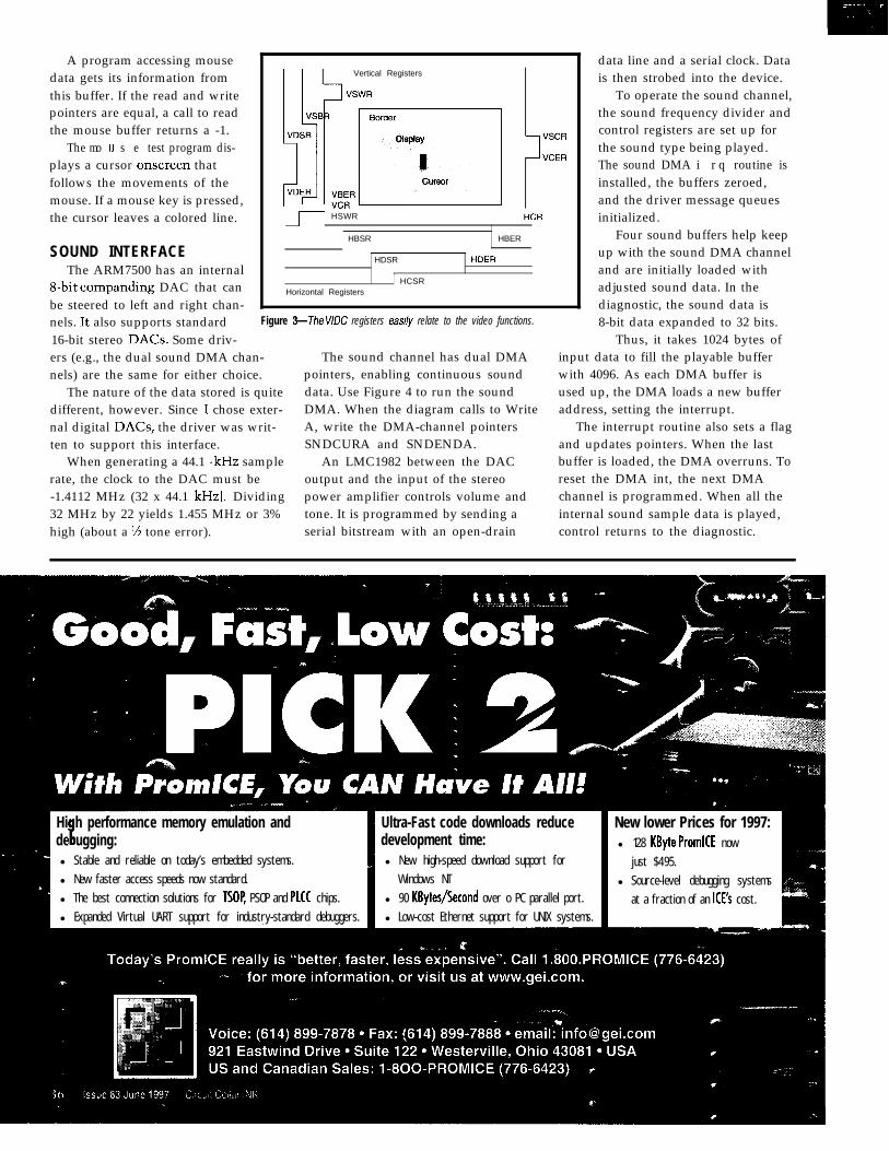
A program accessing mousedata gets its information fromthis buffer. If the read and writepointers are equal, a call to readthe mouse buffer returns a -1.
The mo LI s e test program dis-plays a cursor onscreen thatfollows the movements of themouse. If a mouse key is pressed,the cursor leaves a colored line.
SOUND INTERFACEThe ARM7500 has an internal
s-bit companding DAC that canbe steered to left and right chan-nels. It also supports standard
Vertical Registers
n HSWR--J I
HBSR HBER
HDSR HDER
t HCSRHorizontal Registers
Figure 3-The V/DC registers easi/y relate to the video functions.
16-bit stereo DACs. Some driv-ers (e.g., the dual sound DMA chan-nels) are the same for either choice.
When generating a 44.1 -kHz samplerate, the clock to the DAC must be
The nature of the data stored is quitedifferent, however. Since I chose exter-
-1.4112 MHz (32 x 44.1 kHz). Dividing
nal digital DACs, the driver was writ-
32 MHz by 22 yields 1.455 MHz or 3%
ten to support this interface.
high (about a % tone error).
The sound channel has dual DMApointers, enabling continuous sound
An LMC1982 between the DAC
data. Use Figure 4 to run the soundDMA. When the diagram calls to Write
output and the input of the stereo
A, write the DMA-channel pointers
power amplifier controls volume and
SNDCURA and SNDENDA.
tone. It is programmed by sending aserial bitstream with an open-drain
data line and a serial clock. Datais then strobed into the device.
To operate the sound channel,the sound frequency divider andcontrol registers are set up forthe sound type being played.The sound DMA i rq routine isinstalled, the buffers zeroed,and the driver message queuesinitialized.
Four sound buffers help keepup with the sound DMA channeland are initially loaded withadjusted sound data. In thediagnostic, the sound data is8-bit data expanded to 32 bits.
Thus, it takes 1024 bytes ofinput data to fill the playable bufferwith 4096. As each DMA buffer isused up, the DMA loads a new bufferaddress, setting the interrupt.
The interrupt routine also sets a flagand updates pointers. When the lastbuffer is loaded, the DMA overruns. Toreset the DMA int, the next DMAchannel is programmed. When all theinternal sound sample data is played,control returns to the diagnostic.
Hi h performance memory emulation andde ugging:i6l Stable and reliable on today’s embedded systems.
l New faster access speeds now standard.
l The best connection solutions for TSOP PSOP and PLCC chips.
l Expanded Virtual UART support for industry-standard debuggers.
Ultra-Fast code downloads reducedevelopment time:l New high-speed download support for
Windows NT
l 90 KBytes/Second over o PC parallel port.
l Low-cost Ethernet support for UNIX systems.
New lower Prices for 1997:l 128 KByte PromICE now
just $495.
l Source-level debugging systems
at a fraction of an ICE’s cost.

FLOPPY INTERFACEThe floppy attaches to a stan-
dard I/O Combo chip (FDC37C-663 or 665). It’s programmedexactly as in a PC but at differ-ent addresses. In particular, thesuccessive addresses are on wordboundaries, so 8 and 16-bitoperations are supported.
Finished (stop)
The ARM7500 has a specialchip select (COMBOCS at physi-
Figure 4-The sound DMA has dual data pointers. The program interactswith the hardware to maintain continuous sound outout.
cal address OxO3OlOxxx) to select this IDE INTERFACEpart as well as one that mimics the The RC7500 sports two IDE connec-floppy DMA Acknowledge (CDACK at tions-IDE1 connects to PC Comboaddress 0x03012000). and is located within its address space,
LOGICAL
4‘tart programming devices today with the lowest cost and highest per-formance CERTIFIED programmers. Enjoy a no hassle user interface forALL versions of Windows and DOS. Works with any PC of any speedwithout a hitch. Device libraries added in less 2 hours to our Web cus-tomer support section. Unique programming head options for gang pro-gramming most microcontrollers and memory devices. Direct DockingGangTSOP, QPF, PLCC, DIP... programming heads. Evaluate a unit todaywith 100% satisfaction guaranteed or YOUR MONEY BACK!
(no penalties or restocking fees if unit is returned).
Call Today in USA 800-331-7766303-733-6868 or Visit our Home Page:
w w w.logicaldevices.com
and a separate IDE2. Both haveseparate address spaces for theWestern Digital Hard Disk reg-ister set and the extra floppyregisters for the hard disk.
DOES THE SHOE FIT?Obviously, this information
merely scratches the surface ofwhat the ARM7500 is all about.If your application is along the
lines of an Internet appliance, medicalinstrumentation (e.g., EKG display),and GPS or airport display, the ‘7500 isa chip you should check out. E]
Art Sobel is the hardware applicationsmanager of embedded products at VLSITechnology. He has spent 24 yearsdesigning disk-drive electronics andcontrollers, laser interferometers andprinter controllers, many controllerchips, and speech synthesizers. Youmay reach Art at sobel@ sanjose.vlsi.corn.
75demon.zipand75diag.zipoffer complete source code at<www.circellar.com>. RiscBSD andGNU cross-development software isat <www.ph.kcl.ac.uk/-amb/riscbsd/docs.html> or cftp.netbsd.org>.
ARM7500 Spec Sheetwww.arm.com/Pro+Peripherals/
ASSPs/7500
RC7500, ARM7500 chipsVLSI Technology18375 S. River Pkwy.Tempe, AZ 85284(602) 752-6630Fax: (602) 752-6001
ARM7500 chipsCirrus Logic, Inc.3100 W. Warren Ave.Fremont, CA 94538(510) 623-8300Fax: (510) 226-2180www.cirrus.com/prodtech/
ov.netmobile/ps7500.html
410 Very Useful411 Moderately Useful412 Not Useful
38 Issue 83 June 1997 Circuit Cellar INK@


SINGLE-BOARD COMPUTERThe Dl05330, an industrial computing board for
process- and motioncontrol applications, is available astond-alone board or powered by the company’s Card10
otherboard. It offers operation at thev full industrial temperature range 1-40 to +85”C), a 4” x 7”footprint, access fo’industry-standard software (DOS or Windowspreinstalled, if requested) and onboard interfaces. Targeted em-bedded applications include factory floor automation, hand-heldinstruments, and test equipment.
Onboard features include serial and parallel ports, interfacesfor graphics, hard and floppy disk drives, as well as mouse andkeyboard controllers. It has up to 4-MB DRAM and resident BIOSin 256KB flash memory. Also included are an LCD interface withbacklight control circuitry, programmable watchdog timer, fouranalog-input channels, and a power-management controller.
The Card10 is a fully functional PC/AT motherboard, availablein ‘486 and ‘486DX4 platforms with speeds up to 100 MHz andonboard memory of up to 16 MB.
The Dl05330 and Card10 are sold separately. The Dl05330sells for less than $300 in quantity. The Card10 starts at $800 inquantity. Pricing for evaluation kits starts at $300, dependingon components.
S-MOS Systems150 River Oaks Pkwy.San Jose, CA 95 134- 195 1(408) 922-0200 l Fax: (408) 922-0238www.smos.com
#506
REAL-TIME VIDEO INTERFACE MODULEThe VlPer Vision TEK-380 interfaces automatically to vari-
ous video standards to accommodate noise-free video-display andcapture applications. Designed to complement the company’sVlPer SBCs, the card features up to six composite or three S-videoinputs, NTSC, PAL, and SECAM compatibility, hue saturation,brightness and contrast control, real-time image resizing, andonscreen positioning in a PC/lob form factor. Typical applica-tions include automated shop floor equipment, surveillance sys-tems, personal identification systems, in-vehicle readers and scan-ners, and electronic kiosks.
Other features include CCIR or square pixels for easier imageprocessing, linear zooming with interpolation for smoother edges,full cropping control prior to capture, and the ability to savecaptured images to disk. The card uses the VlPer industrial SBC’sinternal video circuitry to produce full real-time video withoutburdening the system bus for additional bandwidth. Thus, the entiresystem can run at maximum capacity at all times.
The VlPer Vision TEK-380 comes standard with one BNCconnector for composite video, one 4-pin miniDiN for S-video input,and one 14-pin header to handle multiple inputs. Video output isvia a 26-socket header which interfaces to a VlPer industrial board.Both standard and customdesigned software drivers are provided.The unit sells for $395.
Teknor Industrial Computers, inc.7900 Glades Rd.Boca Raton, FL 33434(407) 883-6191Fax: (407) 883-6690 #SO7
-. -. . . _ _
40 ClRClllT (:EIl./\R INK IIJN: 1997

The PC-51 0 single-boord computer combines a 133-MHz’586processor, six serial ports, a GPS interface, advanced video, and48 lines of DIO on a 5.75” x 8” form-factor board. It is designedfor rugged mobile communications, data acquisition, and industrialcontrol applications, and it features an MTBF of 13 years.
The PC-510 supports LCD and Et flat-panel displays, The on-card 65550 video chip acts as a graphics accelerator to support
real-time video. Because the video circuitry oper-ates on the Local bus at full processor speed, high-performance programs like Windows execute very rap Yidly. As well, 2 MB of video RAM is provided to accommo-date a high-resolution display monitor. Power-managementfunctionality is also included. The board also includes a PC/l 04interface, IEEE 1284 multifunctional parallel port, floppy- andhard-drive interfaces, keyboard, speaker and mouse ports, watch-dog timer, real-time clock, 2-MB flash disk, and 1 MB of ED0DRAM (expandable to 33 MB).
The PC-5 10 contains DOS 6.22 in ROM, as well as diagnosticsoftware to test and verify on-card I/O and memory functions. DOSapplications can be stored directly in the resident flash memory,eliminating the need for a hard drive. The card also supports otheroperating systems, such as Windows, Windows 95, Windows NT,and QNX.
The PC-5 10 can operate either in stand-alone mode, or it canbe expanded via its PC/l 04 connector. The unit sells for $995 insmall quantities.
Octagon Systems65 10 W. 91 st Ave. l Westminster, CO 80030(303) 430-l 500 l Fax: (303) 426-8 126 #508
MASS-STORAGE MODULEThe PCM-IDEFLASH-0 is designed for embedded systems requir-
ing low power, high shock and vibrational resistance, instant access todata, and full compatibility with rotational disk drives. Its PC/l 04 formfactor provides up to 84 MB of formatted flash disk storage to replaceconventional disk drives in harsh environments. Applications includeprogram and data storage for data collection and logging, diagnostics,process variables, and setpoints.
The board provides solid mechanical and electrical mounting,permitting a user to install a 1 .8” FlashDrive and cable it to a host
computer’s IDE interface. The drive plugs into a 2-mm connector andfastens securely to the PC board. Since it appears as a standard IDEinterface, no special software drivers or utilities are required. TheFlashDrive products are 100% compatible with DOS, DOS applica-tions, and other operating systems supporting IDE disk drives. It alsooperates with QNX, OS/9000, Lynx, and other real-time embeddedOSs that interface to IDE drives.
The PCM-IDEFLASH-0 comes in an ADP-FLASH version if PC/l 04stack mounting is not desired. It has a 4-pin power connector rather thanPC/l 04 connectors. The PCM-IDEFLASH-0 sells for $50.
WinSystems, Inc. l 715 Stadium Dr. l Arlington, TX 76011(817) 274-7553 l Fax: (817) 548-1358 l www.winsystems.com #509
,JUNE 1997 mpc - 41

’ D S P B O A R D
7
AThe Model C32- 104 is designed for embedded applications
requiring the computational and I/O capabilities of a floating-pointDSP, as well as for DSP algorithm development. It can be operated as
rA
a PC/l O4-bus expansion board or a stand-alone unit, or it can be used A
to control other boards vio the PC/l 04 bus in o system without a host CPUboard. This last mode permits the creation of a lowcost embedded DSPcomputerwith the unit performing functions normally done by the 80386(or higher)CPU board. These functions include the controlling of PC/l 04video, RS-232 serial port, and analog I/O boards.
1
The unit is based on the Texas Instruments TMS320C32 floating-pointDSP operating at 50 MHz, for up to 50-MFLOPS performance. Included on theboard ore 256 KB of zero-wait-state SRAM, 5 12 KB of flash memory, digital I/O, and DSPserial port expansion . ..^. ,
A DSP software-development package containing an assembler, debugger, application examples, andflash-memory programming utilities is included with the board. Price including software is $499 in small quantities.
Dalanco Spry l 89 Westland Ave. l Rochester, NY 14618(716) 473-3610 l Fax: (716) 271-8380 l www.vivanet.com/-dalanco
-huveauPCJust connect a k e y b o a r d ,nonitor/LCD. a disk driveand your ready to run. Or .;brget the drive and bootdirectly from a Flash disk.9dd PC/104 Modules for ’
.?ax/Modem, SCSI, Ethernet,Digital/AnalogI/O, andPCMCIA.3reat for Point Of Sale and WedBrowsers/Servers. Prices start at $200.00 Qty. 1.
* Wide CPU Selection: 386SX. 486DX. DX2, DX4. 586. Pentium.
’ All SBCs have Real Time Clock, Serial. Parallel, IDE, and Floppy.
* On Board Watchdog Timer.
l BIOS with Power Saving Green Mode.
* Wide Bus Selection: PC/ 104, ISA. PCI.
* 10.4” TFT super bright LCD Panel Kits.
l Hardware and Cable kits included for most boards.
618-529-4525 F a x 457-0110 BBS 5295708SlNGLEBOARD 11 EMAC WAY, CARBONDALE, IL 62901
WORLD WIDE WEB: http://www.emacinc.com
?Y122
IliEI
TIRE0 OF WAlTINS FOR THE PROMPT ?
6 DOS IN ROM!
vWDISK1 128k 5 7 5WJISK2 1 4 4 m $ 1 5 0AVOISKB 5 76m $ 1 9 5 $75
Quantity discounts!
$95 EPROMPROGRAMMER
- Super Fast Programming- Easier to use than others- Does 2764127000 [6 Meg1
Marinaok. NHI391 792 8507
8088 SINGLEBOARD
COMPUTER
#123 14 2 CIRCUIT CELLAR INK JUNE 1997

An In-Depth Look at lTLSince FTL-based drivers are becoming more common, you need to know morethan the basics. After discussing FTl technology and algorithms, Raz shows ushow TrueFFS interfaces to many storage devices.
n March 1996, the Personal ComputerMemory Card International Association(PCMCIA) adopted a media-storage specifi-cation called Flash Translation layer (FTL).
Although it was already an industrystandard, FTL picked up speed. The Minia-ture Card Forum also recently proposedthis specification for standard usewith theirnew small form-factor flash card. It’s becom-ing the market’s most widely used andsupported flash file format.
The FTL specification defines the datastructures used to manage PC Cards andMiniature Cards which have a linear arrayof flash-memory chips. Algorithms imple-menting the FTL enable flash to provide fulland transparent hard-disk emulation. So,designers can provide solid-state mass-storage solutions that are lower cost thancards based on ATA technology.
FTL-based drivers are being bundledwith more and more systems, ranging fromdesktops and consumer products (e.g.,digital cameras) to highly customized em-bedded SBCs. In this article, I give you a
look into the FTL technology, its data struc-tures, and the algorithms implementing it.
H I S T O R YThe FTL specification, based on technol-
ogy patented in April 1995, describes avirtual mapping system that enables com-mon flash-memory components to provideull read/write capability.
With a block device driver interface, theimplementation of the algorithms that makeup this mapping scheme lets any flash-memory-based storage device fully emu-late a hard drive’s functionality. The emula-tion is transparent to the host computer’snative OS and file system. Using thesealgorithms, the flash storage medium be-comes a flash disk.
DOS Sector Number
Figure I: Contiguous sectors are mapped to diHerent physical locations on the medium. The FTLkeeps track of their locations via a map fob/e.
45
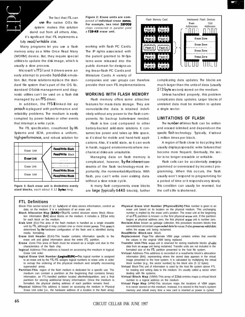
r
7 The fact that FTL canuse the native OS’s file
system makes this solutionstand out from all others. Also,r
’it’s significant that FTL implements a
fully read/writable disk.Many programs let you use a flash
.memory array as a Write Once Read Many(WORM) device. But, they require specialutilities to update the disk image, which isusually a slow process.
Microsoft’s FFS I and II drivers were anearly attempt to provide harddisk emula-tion. But, these solutions replace the stan-dard file system that’s part of the OS. So,standard OS disk management and diag-nostic utilities can’t be used on a flash diskmanaged by an FFS driver.
In addition, the FFS II l inked-list appreach is plagued with performance andreliability problems. The medium is easilycorrupted by power failures or other eventsthat interrupt a write cycle.
The FTL specification, coauthored by M-Systems and SCM, provides a uniform,hrgh-performance, and robust solution for
Figure 2: Erase units are com-posed of individual erase *ones.For example, two Intel 28FoO8chips connected in parallel yielda 128.K8 erase unit.
working with flash PC Cards.The IP rights associated withthe patent granted to M-Sys-tems were released into thepublic domain for designs us-ing linear-flash PC Cards andMiniature Cards. A variety ofcompanies and user groups can thereforeprovide their own FTL implementations.
Flash Memory Card Interleaved Flash DevicesEVHl Odd
Addresses Addresses
complicating data updates. The blocks aremuch larger than the units of data (usually5 12.byte sectors) stored on the medium.
WORKING WITH FLASH MEMORYFlash memory offers some attractive
features for mass data storage. They arenonvolatile-the data is retained indefi-nitely without any power to the flash com-ponents. No back-up batteriesare needed.
Unless handled properly, this problemcomplicates data updates. Larger blocks ofunrelated data must be rewritten to updatea single sector.
LIMITATIONS OF FLASH
Erase Unit
EraseUnit (
Erase Unit
Erase Unit
ReadMRzte BW
Reedh4rEe Black
. . . . . .
..,...
ReadlWttte Blaok
Readlw~Eslodc
Flash is low cost compared to otherbattery-backed solid-state solutions. It con-sumes low power and takes up little space,so it’s ideal for mobile and hand-held appli-cations. Also, it’s solid state, so it can workin harsh, rugged environments where me-chanical disks are unsuitable.
The number of times flash can be writtenand erased is limited and depends on thespecific flash technology. Typically, it’sabout1 million times per block.
Managing data on flash memory iscomplicated, however, bytheinherentcon-straints of the flash technology-most im-portantly, the nonrewritabilityofdata. Withflash, you can’t write over existing datawithout a slow erase cycle.
In many flash components, erase blocks
A region of flash close to its cycling limitusually displays sporadic write failures thatbecome more frequent. Eventually, the sec-tor is no longer erasable or writable.
Flash cells can be accidentally overpro-grammed or overerased by incorrect pro-gramming. When this occurs, the flashusually won’t respond to programming fora period of time or it responds very slowly.This condition can usually be reversed, butFigure 3: Each erase unit is dividedinto evenly
sized blocks, each about 5 12 by+es long. are large.(typically d4-KB blocks), further the cell’s life is shortened.
IFTL DefinitionsBlock-This sector-sized (5 12 byte unit of data stores information, control or)
data, on the medium. It is a subdivision of an erase unit.Block Allocation Map (BAM)-This FTL control structure stores Block Alloca-
tion Information (BAI) about blocks on the medium. It includes a 32.bit entryfor each block on the medium.
Erab Unit (EU)-This area of the flash medium is handled as a single erasableunit by FTL, although it may contain one or more erase zones. This oreo isdetermined by the hardware configuration of the flash and is identified duringmedia formatting.
Erase Unit Header (EUH)-This header contains information specific to theerase unit and global information about the entire FTL partition.
Erase Zone-This area of flash must be erased as a single unit due to thecharacteristics of the flash chip.
logical Address-This address is based on accessing the medium in logicalErase Unit order.
logical Erase Unit Number (logicalEUN)-This logical number is assignedto an erase unit by the FTL. FTL assigns logical numbers to erase units in orderto remap the ordering of the physical medium and simplify recoveringsuperseded areas.
Partition-This region of the flash medium is dedicated for a specific use. Themedium can contain a partition at the beginning that contains binaryinformation, an FTL-handled partition located afterthefirstpartition, and a finalpartition for storing additional binary information. Once the medium isformatted, the physical starting address of each partition remains fixed.
Physical Address-This address is based on accessing the medium in PhysicalErase Unit order [i.e., the hardware address of a location in the flash array).
Physical Erase Unit Number (PhysicalEUN)-This number is given to anerase unit based on its location on the physical medium. This unchangingnumber is implied by the erase unit’s position. The erase unit at the beginningof an FTL partition is known OS the first physical erase unit. If the partitionbegins at physical address zero, the first physical erase unit is number zero.
Reclaim-Also known as garbage collection, this procedure recovers blocks thatweredeleted orcontain supersededdataforreuse. ltalsopreservesvalid datowithin the erase unit being reclaimed.
Read/Write Block-see Block.Replacement Page-This alternate VBM page contains entries that override
the values in the original VBM being replaced.Transfer Unit-This erase unit is reserved for storing read/write blocks ofvalid
data from an erase unit being reclaimed. Transfer units are not included in theformatted size of the FTL partition presented to the host file system.
Virtual Address-This address is recorded in a read/write block’s allocationinformation (BAI), representing where the stored data appears in the virtualimage presented to the host system. It is calculated by multiplying the virtualblock number (e.g., the sector number] by the block size (5 12 bytes).
Virtual Block-This unit of information is used by the host file system above FTLfor reading and writing data to the medium. It’s usually called o sector whendealing with file systems,
Virtual Block Map (VBM)-This array of 32-bit entries maps a virtual blocknumber to a logical address on the medium.
Virtual Page Map (VPM)-This structure maps the locations of VBM pages.It is never stored on the medium. Instead, it is stored in the host’s systemmemory and rebuilt every time a new card is inserted or power is cycled.
CIRCUIT CELLAR INK JUNE 1997
. 7 ISA slots
.486 support
The G486VPC motherboardcombines quality andaffordability with an industrialdesign to meet your needs.Seven full length ISA slotsensure expandability for thecards that you use.
Our engineering staff willgladly discuss custommotherboard designs. FCC& UL certified systems arealso available.
l Six full length l&bit ISA, Oneshared 8-bit ISNPCI slot
l Intel, AMD & SGS-Thomson486 CPU support
l VIA chipsetl Up to 64MB RAM, 256KB cache
FLASH IS COMPLICATED
Because of the nonrewritability of flash,
data must be organized via flash file sys-
tems. Damaging or corrupting the data
(i.e., the low-level format) may mean user
data can no longer be accessed.
Since an accidental or deliberate power
failure, often due to prematurely removing
the flash card, is possible anytime, writing
to the flash must be done in a way that
ensures no loss of existing data.
Even if no flash-hardware errors occur,
the data and recording format must be
coherent at all stages of writing. Also, manu-
facturers use incompatible programming
algorithms to control the flash.
FLASH FILE SYSTEM FUNCTIONA flash file system is a software driver
that makes flash memory emulate a disk
drive. It lets the developer use a common,
well-understood mechanism to store data
on a nonvolatile solid-state medium. The
resulting flash disks may be interchanged
with mechanical disk drives, adding flex-
ibility to the design and debug process.
A well-written flash file system emulates
a disk so transparently that the user and
systemcannotfunctionallydistinguish itfrom
a mechanical disk drive. However, it must
perform low-level operations to accomplish
this as well as overcome the constraints of
flash components.
I examine these operations in detail, but
these features include:
l mapping OS model (disk sectors) to
physical model (flash blocks) as in Fig-
ure 1
endurance
l managing the mapping tables
l maintaining flash erase operations in the
background to optimize performance
l wear-leveling for increased flash-media
Flash MemoryJbdivided into Erase Un
Erase Unit
Erase Unit_______.________
Erase Umt
Erase Unit
Erase Unit
Erase Unit
Erase Unit
Erase Unit
Erase Unit Header
Bkctt Akcatiin Map(BAW
ReadlWrtite BlocksUsed for
Virtual Map Pages.Replacemeol Pages,
and Victuat Btocks
igure 4: Each erase unit has an emse-unitheader (NH) that contains information aboutthe specific unit as well as information aboutthe entire medium.
l detecting errors for mapping bad or
worn-out flash blocks
l protecting existing data and directory
structures for reliability
l implementing different programming al-
gorithms for specific flash components
Before getting into the structure of the
FTL data, look at some terms of the specifi-
cation (see the sidebar “FTL Definitions”).
FTL DATA STRUCTURESAn OS file system (not a flash file system)
randomly updates any block on the system’s
storage medium. But, unless flash is in its
erased state, it cannot accept new data.
FTLdelivers thiscapabilityto higher level
software layers by remapping requests to
write blocks to unallocated or free areas of
the medium and invalidating the area that
previously contained the block’s data. It also
records where the remapped block is placed
for subsequent read accesses.
emulate the standard hard-disk sector size.
In effect, FTL presents a virtual-block
storage device to the higher level software
layers. Virtual block size can be deter-
mined when the storage medium is format-
ted, but it’s normally set to 5 12 bytes to
A Portion of the Block Allocation Mao
Figure 5: In this particular block allocation map (MM), the read/write block size is 5 12 bytes.A/so, the FlI partition does not store checksums, CRCs, or WCs for the virtual-block data.
48#126
CIRCUIT CELLAR INK JUNE 1997
The PC/l 04Motion ControlExperts
Block Offset
Virtual Address
Figure 6: The mapping functionscan be defined as a set of fable-lookup functions based on thenumber of the sector that theoperating system wants to access.
Block OffsetCarried Forward
information about the state of theentire flash medium. All EUHs onthe medium are identical exceptfor their LogicalEUN field values.
Logical Address
Depending on its technology, each flashIC on a PC Card is divided into one or moreerase zones of equal size. Each erase zoneis the minimum contiguous area that can beerased in a single operation.
If 8-bit devices are interleaved to provide16-bit storage, the corresponding physicalzones on two adjacent devices combine asa single erase zone. One device gives evenaddresses, and the other, the odd ones.
An erase unit is a multiple of one or morecontiguous erase zones. Its size is set whenthe medium is formatted (see Figure 2).
For example, if the flash componentsare Intel 28FOO8 FlashFile chips, everychip has sixteen 64-KB erase zones. If twochips are connected on a 16-bit data bus,the erase-unit size is 128 KB.
T R A C K I N G T H E B L O C K SEacheraseunitcontainsalloca-
tion data for the unit’s read/writeblocks. For each read/write block,a four-byte value (i.e., the block-allocation information (BAI)) tracksthe block’s current state.
A read/write block in an eraseunit can be in only one of fourstates-free, deleted, bad, or allo-cated. It can also have one of fourtypes of information-FTL controlstructures, virtual-block data, vir-
tual-block map pages, or replacement pages.The encoded BAI tracks the block’s con-
tent and its state. The block allocation map(BAM) is normally stored immediately afterthe EUH. Some flash contains hidden areasthat store this data instead of using mainstorage space. The type of storage area,main or hidden, is defined in the EUH.
Figure 5 shows the contents of a BAM.Each map entry describes the contents of acorresponding read/write block. This ex-ample uses a 5 12-byte block size, and theFTLpartitiondoesn’tstorechecksums, CRCs,or ECCs for virtual-block data.
The first two read/write blocks store theEUH and BAM. The third (bytes 1024-1535 of the erase unit) holds data for thethird virtual block used by higher level soft-ware layers. The next block (bytes 1536-2047) holds superseded data, and the blockfollowing it has a virtual-block map page.
+
1
k---t--l-i
k
ERASE ZONES AND U N I T S
E R A S E - U N I T H E A D E RFTL divides every erase unit into one or
more equally sized read/write blocks (seeFigure 3). Each read/write block is thesame size as a virtual block (or DOS datasector) used by the host file system.
As shown in Figure 4, each erase unitcontains an erase unit header (EUH) nor-mally located at the beginning of the eraseunit (i.e., offset zero). However, it can bemapped to a different offset.
The EUH contains specific informationabout its erase unit as well as global
V I R T U A L - B L O C K M A PThe BAM tables carry enough informa-
tion for the FTL algorithm to track the virtualblocks and control structures on the me-dium. However, the algorithm required totrack the locations would be slow since itwould rescan the entire medium every timeit looked for the location of a virtual block.
Instead, FTL incorporates an additionalmap on the medium called the virtual-blockmap (VBM). The VBM comprises an array
N eed motion control within yourPC1104 application?
Overwhelmed by the number ofproducts & vendors out there? Lookingfor a motion control specialist insteadof just another PC/ 104 vendor with
Model 5912Encoder Interface
needs of OEMcustomers, Tech80’s family of
PC1104 modules can meet the encoderinterfacing and servo &stepper controldemands of your embedded
Model 5928 environment.
Servo ControllerAND if your needs
extend beyond the PC/104 realm, Tech80 has the industry’s most extensiveline of board-level motion controlproducts for IP, PC, STD and VME-
Stepper Controller regarding yourcurrent project,
please contact us at 800/545-2980 orvisit us at:
Minneapolis, Minnesota USA80015452980 l 6121542-9545 l 6121542-9785 (fax)
www.tech80.com l [email protected]
#12749

r
Figure 7: True-
’FFS and FLite
II- differentinfet-r
Efaces with their ap-
plication but maintainthe same low-level func-
tionality.
tof four-byte entries, each corresponding to a virtual block andcontaining its logical address.FTL uses the virtual-block numberfrom the host as an index into the VBM.
As virtual blocks get assigned to physi-cal blocks, the appropriate entry updatesin the VBM, which is on the medium. So,when an entry is updated to show it hasmoved, the physical block containing theVBM needs to be changed, too. This situa-tion would become a performance issue ifit wasn’t addressed properly, as I’ll discuss.
The VBM storage space is allocatedwhen the medium is formatted. A mecha-nism differentiates between blockscontain-ing data and those holding VBM pages.Blocks with VBM information are treated asvirtual blocks with negative numbers, whilevirtual blocks have positive numbers.
R E P L A C E M E N T P A G EReplacement pages solve any perfor-
mance degradation caused by updatingtheVBMforeveryvirtuaI block thatchangesphysical location on the medium. As itsname implies, a replacement page con-tainsalternateVBMentriesforvirtua1 blocks.
V I R T U A L P A G E M A PThe virtual page map (VPM), the lastmap generated by FTL, is never held on themedium. Instead, it is reconstructed from theVBM contents, which are always on themedium, every time the system is poweredup or a new card is inserted.
Each entry in the VPM tracks the loca-tion of the appropriate VBM page. Sincethe VBM is stored on the medium, thesepages move around as they are updated.
The VPM provides the entry point intothe VBM. Without the VPM, every access tothe medium requires a complete mediascan to find the appropriate VBM.
GElllNG A P H Y S I C A L A D D R E S SFigure 6 shows how a virtual-block num-
ber gets translated into a physical addresswith the required data. It shows some of thekey features of the FTL algorithm. All virtual
50
FintiDelete File
Socket Control
Flash Media
Socket Control
Flash Media
blocks need the same number of addresstranslations to get to the physical address(i.e., accessing two translation maps).
Because of pointer arithmetic and struc-tures sized as powers of two, the arithmeticinvolves very fast simple shift-left and shift-right operations. information in the mapscan always be reconstructed from redun-dant information on the medium.
TrueFFS is a driver intended for an OSwith an existing file system. It typicallycomes in a binary format compatible withthe specific OS and is available for manystandard OSs (e.g., DOS, Windows 3.x,Windows 95 , Windows CE, QNX,VxWorks, pSOS+, etc.).
FLite, which stands for FAT/FTL Lite, is aversion of TrueFFS targeted to applicationswith no built-in file system (i.e., they need afile system and the FTL data format). It’scustomizableand provided with sourcecode.
RECLAIMING UNITS AND BLOCKSTheabilityto reclaim superseded blocks
enables FTL to provide a solution that worksas a writable disk. When the medium isformatted, atleastoneeraseunitissetaside(i.e., a transfer unit). When the medium nolonger has any free blocks, a garbage-collection cycle is executed.
FLite includes DOS FAT file functions, soan application lacking native file-systemcapability can write files directly to theflash media in a DOS-compatible file for-mat. The combination of DOS FAT file andFTL compatibility ensures easy data inter-change between a personal PC and anembedded system.
The transfer unit is always held in anerased state, ready to receive data. Duringthis cycle, the medium is scanned for anerase unit that has garbage blocks.
When a unit is found, blocks with gooddata are transferred to the transfer unit. Toshow that it now contains valid data, thetransfer unit’s EUH is updated. The Logical-EUN field from the unit that had thegarbage data is copied and placedin the transfer unit’s EUH.
This capability may be particularly im-portantwhen using removable flash media(e.g., PC Cards and Miniature Cards).Both FLite and TrueFFS use the same FTLalgorithms and technology.
Where does TrueFFS fit into the system?TrueFFS and FLite are generally used asblock device drivers which sit under the
Once the data is in the transferunit, the old unit is erased and itbecomes the new transfer unit.When data was copied into thetransfer unit, the blocks containinggarbage data were not copied.Thus, when it becomes a new unit, ithas blocks free to accept new data.
I M P L E M E N T A T I O NFTL is a specification for a set of
data structures that provides a mech-anism for tracking the location ofdata on flash media. However, thisspecification doesn’t address all theimplementation issues involved inproviding a fully functional driver
Figure 8: The TrueFFS driver is part of a sotiware stackthat provides a data path from fhe flash media to theOS.
that can provide a robust solution thatinterfaces with an OS or application.
Let’s look at TrueFFS and FLite, whichhave been recognized as the leading implementations of the FTL specification.
T r u e F F S A N D FliteM-Systems has two different forms of FTL
available to developers for use with flashmemory components or cards.
CIRCUIT CELLAR INK JUNE 1997

Sets The PaceIn PC/104
Data AcquisitionScan 16 Channels...
Any Sequence...
DM6420 500 kHz Analog I/O Modulewith Channel-Gain Table and FIFO
With CompanionAm!&86’” 133 MHzPC/l 04 cpuModules
I ,
The CMV586DX133 offersversatile embedded functionality
Our PC/104 and ISA BusProduct Lines Feature
Intelligent DAS Cards WithEmbedded PC and DSP,
Analog and Digital I/O, CPU,Shared Memory, SVGA, PCMCIA,
CAN Bus and GPS Modules
~5!Y7%%t~%~“~ Inc -State College, PA 16804-0906 USA
Tel:1(814) 234-8087 * Fax:1(814) 234-521fURL:www.rtdusa.com
E-MaiI:[email protected]
RTD Scandinavia OyHelsinki, Finland
Tel:358-9-346-4538Fax: 358-9-346-4539
RTD is a founder of the PC/l04 Consortium
52
native file system of the OS (see Figure 7).In thecaseof Ftite, theremay not beanyfilesystem. So, Ftite optionally provides one.
Block device drivers provide:
l compatibility with many file systemsl transparency in operationl compatibility with all file and disk utilities
for the OSl compactness
In Figure 8, you see how TrueFFS fitsinto an OS structure. It may interface to anumber of different flash storage devices.
These may be removable flash cards,an onboard resident flash array, or aseparate flash-disk board (e.g., ISA- orPC/l O&bus boards). In any case, TrueFFSremains unchanged, and the specific inter-face is dealt with in a socket-services layerunder TrueFFS.
In some cases, a Card Services Softwaremanager arbitrates the socket’s operation.This often happens when a system hasmultiple cards (e.g., flash, modems, LAN,etc.), and a specific version of TrueFFS is
necessary.TrueFFS includesstandard memorytech-
nology drivers (MTDs) for common flashdevices used for flash-disk applications.Although these include devices from Intel,AMD, and Samsung and their compatibledevices, there may be a need to add moreexternal MTDs to support other devices.
External MTDs are usually added asplug-in drivers via a standard interface tothe Card Services layer of the software.With Ftite, the MTDs are more often addedvia source code and then implemented asa single monolithic driver.
REFINED ENOUGH?FTL isa robust, industry-standard, proven
flash data format standard that has beenwidely used and adopted. It fully emulatesa hard disk, making flash easy to read and
low-cost, low-power, rugged, reliable storagemedium of choice for hand-held, portable,embedded computer applications. It’s be-
OSs a n d i s a v a i l -able from third-party suppliers for all otherplatforms.
TrueFFS and Ftite are the leading imple-mentations of FTL. They both incorporatethe FTC data format standard to ensureinteroperability across diverse platforms.
(IIK(1IIIT INK 1997
Over the past six years, they have beenrefined in different operating architectures
books, PDAs,
ity, and flexibility of a TrueFFS-based flash-@C
Raz Dan is the customer e n g i n e e r i n g m a n -
ager for M-Systems. He is currently respon-s i b l e for custom applications, advancedtechnical support, and system integrationfor the company’s product /in&. R a z h o l d sa BSEE from Tel-Aviv University. You mayreach him at [email protected].
SOURCESFTL Specification, PC Card Standard, MediaStorage Formats SpecificationPCMCIA2635 N. 1st St.
San Jose, CA 95 134(408) 433.2273Fox: (408) 433.9558
TrueFFS, FLiteM-Systems, Inc.4655 Old Ironsides Dr.
Santa Clara, CA 95054
(408) 654-5820
Fax: (408) 654-9 107
www.m-sysxom
SwapFTL (V.3.0 and up)SCM Microsystems, Inc.
13 1 Albright Way
Los Gotos, CA 95030(408) 370.4888
Fax: (408) 370.4880
www.scmmicro.com
CardWizard, CardWorksSystemSoft, Inc.
2 Vision Dr.
Natick, MA 01760
(508) 65 l-0088
Fax: (508) 65 l-8 188
www.systemsoh.com
PCM+Phoenix Technologies ltd.
2575 McCabe Way
Irvine, CA 92714
(7 14) 440-8000Fax: (714) 440.8300
www.ptltd.com
TrueFFSAflllOSOfl1 1838 Bernado Plaza Ct.
San Diego, CA 92 128-24 14
(619) 673.0870
Fax: (619) 673-l 432
www.annabooks.com
IRS413 Very Useful
4 14 Moderately Useful
4 15 Not Useful

To ROM or Not to ROMTLat is the Question
We all take for granted the three minutes of boot-up time for desktop computers.But, we’d never tolerate such performance in a task-specific system. Rick looksat ways to gain instant response from an embedded PC/7 04 computer.
n embedded system should operatelike an appliance. When you turn it on, youdon’twanttowaithalfaminuteforittobootits operating software from a hard diskdrive. It has to perform its function instantly.
application rather than operating it out ofa disk drive.
a PC/l 04 application. Fooled ya! Here’smy pitch....
Such systems, if they contain microcom-puters, normally load their software instantlyfrom ROM (or EPROM), not disk drives.
There are other reasons why you maynot want an embedded system touse a conventional disk drive. Inapplications with critical data-in-tegrity requirements, “soft” read/write errors are unacceptable.
You’re probably set to hear all aboutROMing a PC/l 06based application. Doyou expect “Rick’s tips” on splitting softwareinto independent code and data blocksthat go in separate ROM and RAM devices?
Well, this month, my mission is to makethe case why you really don’twant to ROM
And, disk drives don’t workover wide temperature ranges, sothey’re usually limited to indoor,temperature-controlled environ-ments. Shock and vibration arealso problems. Size, power con-sumption, and heat generationcan also be reasons to avoid diskdrives in embedded systems.
So, it may seem like a goodidea to ROM your embedded-PC
KEEP AN EYE ON #lYou may have used microcontrollers on
other projects, and you probably ROMedyour application. But, just because that’show it’s done on a microcontroller doesn’tmean it’stherightwayforanembedded PC.
Of course, I assume you wantto harness the full potential of PCcompatibility. While I’m sure you
have a whole slew of reasonsfor using an embedded PC, I’llbet software tops your list.
Wanttosimplifyandenhanceyour embedded project throughthe vast storehouse of PC OS,driver, and development soft-ware? If so, remember: to reapthe benefits of PC compatibility,stay PC compatible!
The PC was designed as adisk operating system (DOS)machine. PC software is always
Photo 1: The tiny DiskOnChip from M-Systems squeezes VP to12 MB of f/ash memory into the same package as a 32pin EPROM.
53JrJNE 1997 -c
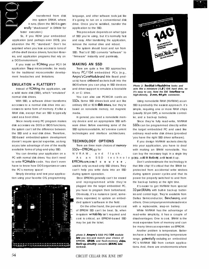
into system DRAM, whereit runs. (Even the BIOS is gen-
’erally “shadowed” in DRAM for
faster execution.)rSo, if you ROM your embedded
application (and perhaps even DOS), youabandon the PC “standard.” Don’t be
transferred from disk
surprised when you lose access to tons ofoff-the-shelf device drivers, function librar-ies, and application programs that rely ona DOS environment.
If you insist on ROMing your PC/l 04application likea microcontroller, be readyfor the traditional microcontroller develop-ment headaches and limitations.
EMULATION = FLATTERY?Instead of ROMing the application, use
a solid state disk (SSD), which “emulates”normal disk drives.
With SSD, a software driver transformsaccesses to a normal disk drive into ac-cesses to some form of memory. It’s like aRAM disk, except that an SSD is typicallyused as a boot drive.
Since nearly every PC program makesdisk accesses via DOS or BIOS functions,the system can’t tell the difference betweenthe SSD and a real disk drive. Therefore,SSD-based embedded-system developmentdoesn’t require special expertise, as longas you take advantage of one of the readilyavailable forms of plug-and-play SSD.
You can develop your application on aPC with normal disk drives. You don’t needto write ROMable code. You don’t evenhave to know how DOS organizes or usesthe PC’s memory space!
Simply develop and test your applica-tion using your favorite OS, programming
language, and other software tools just likeit’s going to run on a conventional diskdrive. Once you’re satisfied, transfer theapplication to the SSD.
This procedure depends on what typeof SSD you’re using, but it’s normally fastand easy. After transferring the application,remove the normal drive and reboot.
The system should boot and run fromSSD. That’s it! SSD converts “software” to“firmware” instantly and painlessly.
MAKING AN SSDThere are quite a few SSD approaches.
Many PC/104 embedded PCs (e.g.,Ampro’sCoreModuleand little Board prod-ucts) have onboard sockets built into theBIOS where you can plug in SSD devicesand driver support to emulate a bootableA: or C: drive.
You can also use PCMCIA cards asSSDs. Some SSD drives look and act likeordinary IDE or SCSI disk drives, but they’rebased on nonvolatile memory, not magneticmedia.
In general, you need a nonvolatile mem-ory device and an appropriate SSD soft-ware driver. Before examining some of theSSD options available, let’s review currenttechnologies and interface architectures.
TECHNOLOGY OPTIONSThere are three main choices of memory-
device technology for SSDs-EPROM,N V R A M , a n d f l a s h .
A s a n S S D t e c h n o l o g y , E P R O M h a sserious limitations. EPROMsare, o f c o u r s e ,
usable only as read-only SSD drives. Theycan’t help you write data into an SSDduring system operation.
Since EPROMs generally can’t be erasedand reprogrammed while they’replugged into the target embedded PC,you have to program them beforehand.Obviously, it’s a nuisance (and, some-times, expensive) to update an embed-ded system’s software in the field.
On the other hand, the per-unit costof EPROM SSD can’t be beat. So, whenin-system writability isn’t required andcost is critical, an EPROM-based SSDmay be just the ticket.
photo 3: Ampro’s SSD PC/ ID4 modulelets you mix-and match your choice ofEPROM, HAM, and flash-memory chbs.Back-up circuib converts SRAMs- intoNVRAM.
Photo 2: SanDisk’s FlashDrive looks andacts like a miniature (l.S’g IDE hard disk, soit’s easy to use. Note the IDE intetfac-high-density, 2-mm, 44pin connector.
Using nonvolatile RAM (NVRAM) as anSSD is probably the easiest approach. it’ssimple, requiring one or more RAM chips(usually 32-pin DIP), a nonvolatile control-ler, and a back-up battery.
Since they’re fully read-write, NVRAMSSDs can be programmed directly withinthe target embedded PC and used likeordinary read-write disk drives (provided‘you have the right SSD driver software).
If you design NVRAM sockets directlyinto your application, you have to dealwith making an SRAM nonvolatile. Youcan buy the necessary logic in a single tinychip, add a battery, and hook it up.
Don’t underestimate the technology inthat little chip! It’s critical that the SRAM beprotected from accidental write strobesduring system power cycles and that itspower be properly switched to and fromthe back-up battery at the right time.
It’s easier to get NVRAM from special32-pin SRAMs with built-in back-up batter-ies and control logic. They’re available fromDallas Semiconductor, Benchmarq, andothers. Onecompanyevenmakesadevicewith a replaceable, snap-on battery.
While NVRAM has the advantage ofread-write simplicity, it has a couple ofdisadvantages. One is cost. SRAM is themost expensive form of memory and canbe many times as expensive as EPROM.
Another problem is temperature. Batter-ies have a limited operating temperaturerange, potentially excluding an embeddedPC’s NVRAM SSD from certain applica-tions. And, there are environments where
CIRCUIT CELLAR INK JUNE 1997

M-Systems offersupto32MBof
flash memory on thisPC/ ID4 SSD module. The
product’s support softworeworks with DOS, Windows,
VIVA, ana vxwor~s.
batteries aren’t allowed due totheir corrosive (sometimes explo-sive) chemicals.
Of course, batteries don’t lastforever. Systems with NVRAM SSDseventually need their batteries re-placed, which can be inconvenientand costly. It also means expen-sive system down time and loss of valuabledata.
So, if NVRAMs have all these problemsand EPROMs are read-only, can any othermemory technology work well as an SSD?That brings us to..
FLASH MEMORYFlash is closely related to EPROM. But,
some clever semiconductor scientists fig-ured out how to use quantum effects tomake an EPROM that can be erased andreprogrammed electrically.
“isn’t that an EEPROM?” you might ask.Not exactly.
EEPROM was the first form of electri-tally erasable/programmable ROM. But itwas more expensive than SRAM! Flash isonly slightly more expensive than EPROM.
Unfortunately, flash isn’taseasytoeraseand reprogram as SRAM. But given its lowcost, so what if it takes a little extra effort!
Flash-device erasing and programmingrequirecareful attention todetails. Data andwrite control signals must sequence justright or the data neither records nor pro-grams fully into the memory cells.
Also, flash wears out. It only lasts aspecified number of erase/write cycles.Fortunately, it’s rated for hundreds of thou-sands of cycles, and there are ways tomanage its lifecycle.
One method is to reread the data afterwriting to a flash location to verify that itwas written successfully. As the locationwears out, you might need to write the dataseveral times to get it to program success-fully. Eventually, it fails completely, but itdoes extend the life of flash for a while.
If a flash device needs to be writtenmany times, it’s critical that the writes be
56
evenly distributed or it may wear out pre-maturely. It’s like rotating your car tires. Thisprocess--called “wear leveling”-is a criti-cal function of flash support software.
As if this wasn’t enough, flash doesn’tlet you rewrite a single location. You musterase and rewrite some minimum blocksize. Blocksize has been steadily shrinkingas flash technology evolves, so it’s disap-pearing as a key issue. But, it used to be anentire chip, which caused some interestingSSD implementation challenges.
Nowyou track”clean”and “dirty” blocks.New data is always written into cleanblocks. And, blocks with data that’s nolonger current are marked “dirty.”
After a while, a flash device can be fullof dirty blocks even if it’s nearly empty from
a DOS perspective. When this happens,the flash-managementsoftwareconsolidatesthe good data, making new clean blocks,in a process called “garbage collection.”
Flash-management software carefullymaintains tables of clean and dirty blocks.
Doing this, while maintaining the gooddata’s integrity, is tricky. Don’t try it at home!
Fortunately, several sources of off-the-shelf flash file system (FFS) software do agood iob of making flash work reliably. Apopular one is TFFS from M-Systems.
NAND VERSUS NORThe flash memory I’ve been talking about
is NOR. There’s a new development in flashcalled NAND. The two names refer to howthe logic inside the devices is structured.
I won’t try to explain the internal differ-ences (OK, so I don’t really know!). But, Iwant to point out a couple of key functionalissues that affect how they’re used.
NOR flash is accessed a lot like EPROMor SRAM, except for the restrictions I men-tioned. You put an address on its addresspins, and you read or write data on its datapins. It can even plug into an EPROM socket.
NAND flash is accessed in more of aserial datastream manner. In this sense, itacts a little more like a disk drive.
NAND flash was developed as a disk-likestorage medium fordigital camerasandhand-held computers. So, it’s no surprisethat it’s quicker to program, has conve-niently small erase-block sizes, and boastsa high erase/write endurance.
Now for the bad news. NAND is just astricky as NOR, but for other reasons. Forone thing, you don’t talk to it like an SRAMor EPROM. You need special circuitry tointerface it to the system.
Another problem: NAND devices comewith defects, just like hard disks. You needto test for and map out the defects.
As with disk drives, it’s useful to includeerror detection and correction using CRClogic. You need a special controller chip-
Device System Interface Size (in.)Sustained Sustained
Max. Cap. Read Rate Write Rate
EPROM chip 32-pin DIP 1.8 x 0.6 x 0.3 1 MB fast (read only)NVRAM module 32-pin DIP 1.8 x 0.6 x 0.4 512 KB fast fastNOR flash chip 32-pin DIP 1.8 x 0.6 x 0.3 512 KB fast (read only)DiskOnChip, NOR 32-pin DIP 1.5x0.6x0.3 2MB fast slowDiskOnChip, NAND 32-pin DIP 1.8 x 0.75 x 0.3 12 MB fast medium1.8” IDE Flash drive IDE 3.0 X 2.0 X 0.4 240 MB medium mediumCompactFlash IDE 1.4 X 1.7 X 0.2 20 MB medium mediumPC/l 04 Flash Disk PC/l 04 3.6 x 3.8 x 0.6 32 MB fast slowMiniModule/SSD + EPROMs PC/i 04 3.6 x 3.8 x 0.8 4MB fast (read only)MiniModule/SSD + SRAMs PC/l 04 3.6 x 3.8 x 0.6 2MB fast fastPCMCIA-ATA PCMCIA 3.4 X 2.1 x 0.1 300 MB medium mediumPCMCIA linear flash PCMCIA 3.4 x 2.1 X 0.1 64 MB medium mediumPCMCIA linear NVRAM PCMCIA 3.4 X 2.1 X 0.1 64 MB fast fast
Table 1: There are four main SSD approaches used in PC/104 systems-chip-like modulesplugged info 32pin DIP sockets, drive-like modules connected to an IDE intetface, specializedPC/ 104 modules full of flash, EPROM, or NVRAM devices, and cards plugged inio PCMCIAslots.

Photo 5: PCMCIA fitsneaf/y into PC/l 04
applications and suppo~sall the key SSD apprvaches,
including linear flash (shown),ATA-flash, and NVRAM. Ampro’s
PC/ 104 adapter (also shown) hasslots for two PCMCIA cards.
and software-to effectively use NANDflash chips as SSDs.
By now, I’ve probably scared you sobadly you’re ready to turn the clock back20years and return to ROM-based micro-controllers. But, don’t despair!
There are quite a few easy-touse,plugand-play SSD solutions ready to serveyour PC/l 04 embedded-PC needs.
BYTE-WIDE DEVICESMost PC/104 embedded PCs include
one or more 32-pin bytewide memory-device sockets. These were originally in-tended for simple DIP or PLCC EPROM andSRAM chips.
Using these devices, the capacity of a32-pin socket is limited to 1 MB for EPROMsand 5 12 KB for SRAMs. Depending on theSSD driver, multiple byte-wide sockets cancombine into a single DOS drive letter forlarger SSD capacity.
As 32-pin NOR flash surfaced, it’s beensupported like an EPROM, except that itcan be reprogrammed-usually on a fulldevice basis-inside the system.
The simple byte-wide SSD is pretty lim-ited in capacity (comparable to a floppy).Although a few PC/l 04 applications runout of one or two simple byte-wide chips,storage requirements have exploded withCPU performance and memory availability.
A nice solution to the limitations of thesimple 32-pin byte-wide SSD is providedby M-Systems’ DiskOnChip flash module,shown in Photo 1. Although it’s the samesize as a 28- or 32-pin DIP EPROM, thiscompact device has up to 2 MB of NOR, orup to 12 MB of NAND, flash. Itcontains thenecessary circuitry to look just like a simpleDIP EPROM to the PC/l 04 CPU.
DiskOnChip comes complete with TFFSand other support software for formatting,operation, and maintenance. Future ca-pacities are expected to reach 72 MB.
The original NOR version of DiskOnChip(DOC 1000) had relatively slow write-cycletime and long garbage-collection laten-ties. However, the new higher capacity
58
version (DOC2000) benefits from the fastwrite cycles and small erase block sizes ofNAND technology.
In fact, every memory technology I men-tioned (i.e., NVRAM, EPROM, various kindsof flash) is available on PCMCIA cards,which are beginning to be called “PCCards,” by the way.
DRIVE-LIKE MODULESSeveral companies now offer small size
(1.3” and 1.8” form factor) SanDisk flashdrives that look precisely like small IDEhard disk drives (see Photo 2). They havethe same physical footprint, mounting holes,interface connectors, and functional inter-face as their magnetic media counterparts.
As a plus, PCMCIA cards are remov-able. They can be inserted and removedwhile the system is running, just like floppydisks. They’re useful for storing data, load-ing parameters, and updating firmware.
Since PCMCIA cards are popular forlaptop PCs, they are sold by all majorcomputer retailers at competitive prices.
With IDE flash, a microcontroller handlesall flash-management functions (e.g., wearleveling), so no special drivers are needed.IDE flash was pioneered and popularizedby SanDisk (formerly SunDisk) and is avail-able in 4-300-MB capacities, with highercapacities on the way.
But PCMCIA cards require a specialPCMCIA card slot. You can’t just plug theminto a byte-wide memory socket or cablethem to an IDE interface. Instead, you needa PCMCIA controller or interface module,adding cost and complexity.
To use these tiny IDE flash drives, justinstall and operate them like nor-mal IDE drives. Nothing’s simpler!
If you don’t need them as removablemedia, check out a DiskOnChip or an IDEflash drive. On the other hand, you mayneed NVRAM for its speed and truly unlim-ited rewritability, and PCMCIA is the best
One possible catch: you needan IDE interface in your system.However, most PC/l 04 CPUs nowinclude IDE interfaces free.
One major advantage: IDE flashdrives are OS independent. Alloperating systems provide IDE harddisk support, and flash-management is handled by the drive. Youcan replace the drive without wor-rying about having the properdriver for the specific flash technol-
ogy. Photo 6: Although the jury’s sti/l out on which mem-orv-card format will be the lona-term favoriie for
cated PC/l 04 module? This option, too, isreadily available in a variety of formats.
PC/l 04 SSD modules come with fouror more 32-pin byte-wide sockets for indi-vidual plug-in EPROM, SRAM, or flash(e.g., Ampro’s MiniModule in Photo 3).They’re also available with soldered onNOR flash for up to 32-MB SSD capacity(e.g., the M-Systems PC/l 04 Flash Disk inPhoto 4),
PCMCIA MEMORY CARDSLast, but certainly not least, is PCMCIA
(see Photo 5). This well-known standardoffers a broad range of SSD capabilities.
PC/l 04 SSD MODULES di&l cameras, these tiny Sanbisk Compactflash
Why not put EPROM, NVRAM,cards certainly meet the needs of PC/ 104 applica-
or flash SSD devices on a dedi-tions requiring highly compact and removable flash-memory modules.
CIRCUIT CELLAR INK JUNE 1997
way to contain high capacity, reasonablypriced NVRAM.
Incidentally, PCMCIA offers two differ-ent flash-card configurations.
SanDisk’s PCMCIA-ATA is functionallyidentical to an IDE flash drive, except it’saccessed through a PCMCIA card slotinstead of an IDE interface.
From a command-set perspective, it pro-vides the identical system-level interface asIDE. It’s even possible to create a passiveadapter between PCMCIA-ATA flash cardsand standard IDE interfaces, eliminatingthe need for a PCMCIA controller.
Like IDE flash drives, each PCMCIA-ATAcard has an internal controller to handleflash-management and IDE command-setfunctions. (ATA means ATattachment inter-face. It’s just another name for IDE.)
The other PCMCIA flash approach cor-responds to that used in the DiskOnChip(see Photo 5). It is commonly referred to as“linear flash” because the flash is indirectlyaccessible (via bank switching) to the sys-tem CPU as blocks of linear memory. Therequired bank-selection logic is locatedwithin the PCMCIA interface controller.
Although linear-flash PCMCIA cardsdon’t bear the burden ofan internalcontroller,this is also their biggest shortcoming.
With no internal controller to automati-cally manage flash-memory wear-levelingand erase/write functions, these tasks mustbe handled by the system CPU, resulting inreduced real-time performance and creat-ing a degree of OS dependence.
Also, when you change cards, you mustensure that your embedded system has theright driver software to properly handle thecard’s internal flash technology.
NEWS FLASHWe can’t leave the subject of SSD for
PC/l 04 applications without looking at thelatestdevelopments-solid-statestoragefordigital cameras.
Have you noticed ads for filmless digitalcameras? Photography’s going digital!
Whether this is good or bad for photog-raphers, I can’t say. But for PC/104 em-bedded systems, it means SSD media-especially flash-is about to become lessexpensive and more widely available.
Unfortunately, there isn’t a consensus onexactly what tiny memory-card standardwill prevail. Sound familiar?
So far, SanDisk’s CompactFlash hasmade the most inroads. Shown in Photo 6,
it’s essentially a shrunken version ofPCMCIA-ATA.
Like its big brother, CompactFlash hasan IDE-like functional interface. It’s relativelyeasy to convert from an IDE hard driveinterface to a CompactFlash card socket.
While this sounds like a dream cometrue for embedded systems needing minia-ture removable SSD cards, CompactFlashand two other tiny memorycard standardsare fiercely battling for dominance in thedigital-camera market.
For sure, you’ll be hearing a lot aboutnew flash-memory alternatives to disk drives.
P U T T I N G I T T O G E T H E RAs you can see, PC/l 04 system design-
ers have many options. To help you evalu-ate the alternatives, take a look at Table 1.
I hopeyou’refeeling more enlightened-rather than more confused-than before. Ifnot, don’t worry. It’ll probably all come toyou-in a flash! K$.EK
Rick Lehrbaum cofounded Ampro Com-puters where he served as VP of engi-
neering from 1983 to 1991. Now, inaddition to his duties as VP of strategicdevelopment, Rick chairs the PC/l 04Consortium. He may be reached at
SOURCESMiniModule/SSDAmpro Computers, Inc.990 Almanor Ave.Sunnyvale, CA 94086(408) 522-2 100Fox: (408) 720-l 305V,VW.Clmpro.com
DiskOnChip, TFFSM-Systems, Inc.4655 Old Ironsides Dr.Santa Clara, CA 95054( 4 0 8 ) 6 5 4 5 8 2 0Fax: (408) [email protected]
PCMCIA-ATA, FlashDisk, CompactFlashSonDisk Corp.140 Caspion Ct.Sunnyvale, CA 94089(408) 542-0500Fax: (408) 542-0503
MiniahweCardIntel Corp.500 W. Chandler Blvd.Chandler, AZ 85226-3699( 6 0 2 ) 5 5 4 8 0 8 0Fax: (602) 5547436www.intel.com
HRS4 16 Very Useful
4 17 Moderately Useful418 Not Useful
-
I
EP
!
.
.
.
.
.
.
.
.
.
.
132
IF YOU DO
FUNCTIONAL
YOU NEED
YOTSl4t54RPMGELECI’RONICEXTENDERS
E!.e&onii I’CI Extender/Pa Mini Extender
- ---
InserVFfemove Cards With PC Power On!
Save Time Testing And Developing Card!
Save Wear On Your PC From Rebooting
Adjustable Overcurrent Sensing Circuitry
NO Fuses, All Electronic For Reliability
Single Switch Operation W/Auto RESET
Optional Software Control Of All Feature
Breadboard Area For Custom Circuitry
And More...
Passive PCI Extender Passive EISA Extender
Passive MC32 Extender Passive ISA Extender
1
7 AZ-COM, INC. ‘).
24-Hour Fax on Demand:510-947-l 000 Ext.7
EMell: [email protected]
VNTOU?HOMEPA6EAT:
http://az-com.coml
59

Fred measures and stores voltages at specified times using National’sNS486SXF. He shows how to get the ADC data into the ‘486 for processing,store the data to EEPl?OM, and use Vetra’s Reverse Pipe for keyboard access.
T11) It s a most time. I tense up as I await my
cue. We’re on the air.“Hi, I’m Fred Eady. Welcome to the
Circuit Cellar Florida Room. Today’s spe-cial guests are National Semiconductor’sNS486SXF and Vetra Systems’ ReversePipe.” (Huge applause from the audience.)
I turn around quickly, drop the mic, andtrip over the cord. As I fall on my face infront of a live studio audience, I mumble,“Oh, @*#$!”
I turn to greet my guests, and they’remachines! A PC board filled with all sortsof components and a rather tinyblack box laden with I/O connec-tors sit by my desk!
Blahnn. Blahnn. Blahnn. Wake up, sleepyhead. I slap the alarm button and thinkabout how I hate that noise. Boy, anotherweird dream. Better get up and get with it.I’ve got an article to write.
Most guys sleep soundly and dream ofbeautiful women, wealth, and fame. Notme. My Vanna is a piece of embeddedsilicon dressed in sexy software lace. Mywealth? It’s firmware that’s either gone upin a flash or stored in a spinning magneticvault. Fame? Well, it’s the 15 minutes or soa month from those of you thot follow myadventures in INK’s Florida Room.
But since this offering startedout as a talk show, let’s meet theguests.
“Oh, no!” I think. “I don’t haveany software to make them talk!”(We’reon a talkshow, you know.)
I frantically call to the set’s bestboy, “Get my embedded develop-ment software and that VIPer806out here quick!”
I yell to the set director, Mark,“Roll a couple commercials backto back. That’ll give me time to getthese things hooked up! Did youbring that Iittlex-ytable? We mayneed it for fill.”
Photo I: This beauty can turn any embedded programmer’s head.Note the abundance of header pins surrounding the NS486SXF.
60 CIKCIJIT CELIAK INK JllNE 1997
N A T I O N A L ’ S NS486SXFNormally, when you think of
National Semiconductor, you thinkcomponents. You know-regula-tors, logic ICs, things like that.
Sure, there’s the NationalCOP8 series of microcontrollers,but National never really spelled“embedded” like you and I do.
For the next few minutes, we’regoing to put the new NS486SXFevaluation board to work.
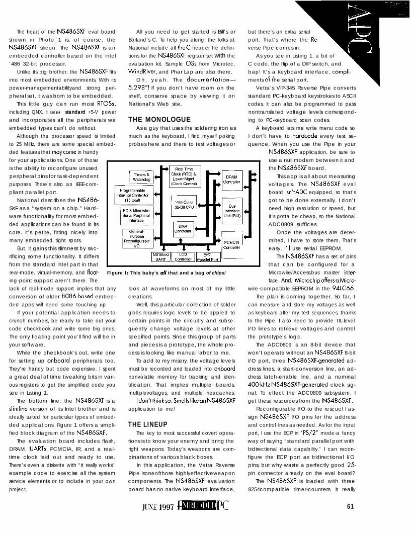
The heart of the NS486SXF eval boardshown in Photo 1 is, of course, theNS486SXF silicon. The NS486SXF is anembedded controller based on the Intel‘486 32-bit processor.
Unlike its big brother, the NS486SXF fitsinto most embedded environments. With itspower-managementabilityand strong peri-pheral set, it was born to be embedded.
This little guy can run most RTOSs,including QNX. It uses standard +5-V powerand incorporates all the peripherals weembedded types can’t do without.
Although the processor speed is limitedto 25 MHz, there are some special embed-ded features that maycome in handyfor your applications. One of thoseis the ability to reconfigure unusedperipheral pins for task-dependentpurposes. There’s also an IEEE-com-pliant parallel port.
National describes the NS486-SXF as a “system on a chip.” Hard-ware functionality for most embed-ded applications can be found in itscore. It’s petite, fitting nicely intomany embedded tight spots.
But, it gains this slimness by sac-rificing some functionality. It differsfrom the standard Intel part in that
All you need to get started is Bill’s orBorland’s C. To help you along, the folks atNational include all theC header file defini-tions for the NS486SXF register set with theevaluation kit. Sample OSs from Microtec,WindRiver, and Phar Lap are also there.
Oh, yeah. The documentation-5.298”! If you don’t have room on theshelf, conserve space by viewing it onNational’s Web site.
THE MONOLOGUEAs a guy that uses the soldering iron as
much as the keyboard, I find myself pokingprobes here and there to test voltages or
but there’s an extra serialport. That’s where the Re-verse Pipe comes in. 1
As you see in Listing 1, a bit ofC code, the flip of a DIP switch, andbap! It’s a keyboard interface, compli-_ .
Vetra’s VIP-345 Reverse Pipe convertsstandard PC-keyboard keystrokes to ASCIIcodes. It can also be programmed to passnontranslated voltage levels correspond-ing to PC-keyboard scan codes.
A keyboard lets me write menu code soI don’t have to hardcode every test se-quence. When you use the Pipe in your
ments ot the serial port.
real-mode, virtual-memory, and float- Figure 1: This baby’s a/I that and a bag of chips!
ing-point support aren’t there. Thelack of real-mode support implies that anyconversion of older 8086-based embed-ded apps will need some touching up.
If your potential application needs tocrunch numbers, be ready to take out yourcode checkbook and write some big ones.The only floating point you’ll find will be inyour software.
While the checkbook’s out, write onefor setting up onboard peripherals too.They’re handy but code expensive. I spenta great deal of time tweaking bits in vari-ous registers to get the simplified code yousee in Listing 1.
The bottom line: the NS486SXF is aslimline version of its Intel brother and isideally suited for particular types of embed-ded applications. Figure 1 offers a simpli-fied block diagram of the NS486SXF.
The evaluation board includes flash,DRAM, UARTs, PCMCIA, IR, and a real-time clock laid out and ready to use.There’s even a diskette with “it really works”example code to exercise all the systemservice elements or to include in your ownproject.
look at waveforms on most of my littlecreations.
Well, this particular collection of solderglobs requires logic levels to be applied tocertain points in the circuitry and subse-quently change voltage levels at otherspecified points. Since this group of partsand pieces is a prototype, the whole pro-cess is looking like manual labor to me.
To add to my misery, the voltage levelsmust be recorded and loaded into onboardnonvolatile memory for tracking and iden-tification. That implies multiple boards,multiplevoltages, and multiple headaches.
Idon’tthinkso.Smellslikean NS486SXFapplication to me!
THE LINEUPThe key to most successful covert opera-
tions is to know your enemy and bring theright weapons. Today’s weapons are com-binations of various black boxes.
In this application, the Vetra ReversePipe isoneofthose highlyeffectiveweaponcomponents. The NS486SXF evaluationboard has no native keyboard interface,
NS486SXF application, be sure touse a null modem between it andthe NS486SXF board.
This app is all about measuringvoltages. The NS486SXF evalboard isn’tADC equipped, so that’sgot to be done externally. I don’tneed high resolution or speed, butit’s gotta be cheap, so the NationalADC0809 suffices.
Once the voltages are deter-mined, I have to store them. That’seasy. I’ll use serial EEPROM.
The NS486SXF has a set of pinsthat can be configured for aMicrowire/Access.bus master inter-face. And, MicrochipoffersaMicro
wire-compatible EEPROM in the 94LC66.The plan is coming together. So far, I
can measure and store my voltages as wellas keyboard-alter my test sequences, thanksto the Pipe. I also need to provide TTL-levelI/O lines to retrieve voltages and controlthe prototype’s logic.
The ADC0809 is an 8-bit device thatwon’t operate without an NS486SXF 8-bitI/O port, three NS486SXFgenerated ad-dress lines, a start-conversion line, an ad-dress latch-enable line, and a nominal400-kHz NS486SXF-generated clock sig-nal. To effect the ADC0809 subsystem, Iget these resources from the NS486SXF.
Reconfigurable I/O to the rescue! I as-sign NS486SXF I/O pins for the addressand control lines as needed. As for the inputport, I use the ECP in “PS/2” mode-a fancyway of saying “standard parallel port withbidirectional data capability.” I can recon-figure the ECP port as bidirectional I/Opins, but why waste a perfectly good 25-pin connector already on the eval board?
The NS486SXF is loaded with three8254compatible timer-counters. It really
61

$* 80251 Embedded ‘{
Midwest Micro-Tek is proud to offer $its newest line of controllers based ’on the 8031/51/251 architecture.The 8031 comes to at a surprisingly
s
low cost of $89.00 (100 quantity).i
MIDWEST MICRO-TEK2308 East Sixth Street
680~0,683~~ Pow&C” family80386 protected mode80x86/88 real mode
i96@ familyRXXO, LR33xxx
l Compact, ROMable, fast intetmpt responsel Preemptive, priority based task schedulerl Mailbox, semaphore, resource, event, list,
buffer and memory managersl Configuration Builder utilityl Comprehensive documentationl No royalties, source code included
For n sampk of Kwiklookand desniption ofAh4X,Phone: (604) 734-2796Fax: (604) 734.8114E-mail: [email protected] e b : http://ww.k&k.ca
KADAK Products Ltd.206-1847WestBroadwaVancouver,BC,Canada V$J lY5
2 If you’re interested in getting the \f most out of your project, put the a‘9 most into it. Call or Fax us for corn- t+ plete data sheets and CPU ootions. $
t MIDWEST MICRO-TEK
shows its embedded roots here. The timer-counter pins, including thegates, are physi-callyaccessible! Boom! There’sour400-kHzADC0809 clocksource. The hardware parti-culars can be gleaned from Figure 2.
BEHIND THE SCENES
With the problem defined and hardwareresources in place, let’s bring the projectalive module by module. I’ll start with theECP peripheral baseaddressed at 0x0278.
All ECP functionality is selfcontained inthe NS486SXF. ECP port operation is con-trolled via the contents of the NS486SXFparallel-port I/O control registers, whichare mapped in I/O space for easy access.
Of the six possible ECP modes of opera-tion, I chose PS/2compatible mode. I en-abled it by setting bit 5 in the ExtendedControl Register (ECR) at location Ox067A.
The ECR’s three highorder bits deter-mine which mode the port operates in. ForPS/2 mode, the mask is 001. The remainingECR bits twiddle with the IRQ, FIFO, andDMAelements. Since I’m not using the otherECP modes, these bits are don’t cares.
Once the port mode is set, the only thingleft is set the port data direction. Since theECP is used for input only, I set bit 5 of theDevice Control Register (DCR) located ataddress Ox027A to enable the ECP dataI/O pins as inputs.
If I needed bidirectional capability, Icould toggle the state of bit 5 in the DCRusing ASMOP (A Simple Matter Of Program-ming). Thatway, I could determine whetherthe ECP data pins were inputs or outputs.
The ECP is ready to roll. If the 0x0278address looks familiar, it’s because theNS486SXF architecture tries to-retain stan-dard PC I/O addressing where possible.
I N T E R V I E W I N G A - T O - D
Now I need three address lines and onALE (Address Latch Enable) line for theADC0809. These lines are part of anonboard multiplexer arrangement selectingone of eight analog inputs. The ADC0809also requires a start conversion (SC) pulseI can piggyback onto the ALE line.
The analog-input port address is clockedinto the ADC0809 on the rising edge of the
Usthtg I: Like Barry Manilow says, “I write the wde that makes the whole thing sing. m
i n t m a i n 0 1i n t i ;i_inp(ECP_ECR); // turn on PS/Z modei 1 0x20:outp(ECP_ECR,i);
i_inp(ECP_DCR); // set ECP direction biti 1 0x20;outp(ECP_DCR,i);
i_inp(RIO_CONTROL): // disable LCD/PCMCIA functionsi 1 OxCO; // and steal pins 48-54 and 68-79outp(RIO_CONTROL.i):
7 OxFF; // set stolen pins -for output_outp(RIO_DD_BYTE2.i);outp(RIO_DD_BYTE3,i);
~_inp(BIU_CONTROLl);// write bit masks to RIO_DO_BYTEX// enable PIT and Microwire
i 1 0x88:_outp(BIU_CONTROLl.i);_outp(PIT_CONTROL,Ox5E); // initialize PIT_outp(PIT_COlJNTl,Ox04):_outp(PIT_CLOCK,Ox02);_outp(PIT_TICR.OxEA):_outp(TWI_CONTROL.OxFC); // initialize MicrowireoutpCTWI_U_CONTROL,OxF2);
7 _inp(UART_MSC);i & OxFB:_outp(UART_MSC,il;outp(UART_CLOCK,27);
i_inp(UART_CLOCK):// set clock to 25 MHz
// Initialize UART and baud rate here...d o // read char from Pipe and print to PC
inp(Ox3FD);wh~leT~i&OxOI~!OxOI~:i_inp(Ox3F8);printf("Ox%x\n".i):return 0;
1,
/
CIRCUIT CELLAR INK JUNE 1997
i
SC pulse,time. Theedge of t
Sinceor PCMCtheir pinsdress antI/O (RIO]
NS48include fUART lintLCD interfinterface7oftheRthe LCD a15 pins fs
As FigSXF pins 1with pin 7generatoltheir function Regi!
The DIlocationslays out 1DDR bits,althoughan outpui
Writincontrol rfputs the 1single-chischeme,pedance
The DcOxEFCC-each reccsignals aare outpuNS486S:makes shplexer sui
Next400-kHz 1NS486S:(PIT) to g’
Progrcby manit0x0040-identical Irun-of-the
Gettinfrequent)PIT is actInterface2. This taof the BllOxEFOO.

SC pulse, and the ADC is initialized at thattime. The conversion begins on the fallingedge of the SC pulse.
Since I’m not using the NS486SXF LCDor PCMCIA peripherals, I can reconfiguretheir pins as the ADC0809 multiplexer ad-dress and latch lines. The ReconfigurableI/O (RIO) Control Register lives at OxEFCO.
NS486SXF reconfigurable peripheralsinclude four CS (chip select) lines, twoUART lines, the ECP port (eight lines), theLCD interface (seven lines), and the PCMCIAinterface (eight lines). By setting bits 6 and7 of the RIO Control Register, I can disablethe LCD and PCMCIA functionality, freeing15 pins for general-purpose I/O.
As Figure 2 shows, I assigned NS486-SXF pins 68,69, and 70 as address lines,with pin 71 acting as the ALE and SC pulsegenerator. All these pins are outputs, andtheir function is defined in the Data Direc-tion Register (DDR).
The DDR is 32 bits wide and resides atlocations OxEFC4-OxEFC7. The datasheetlays out what pins correspond with whatDDR bits, so trust me. I chose the right ones,although I thought it odd that 1 made a pinan output and 0 signified an input.
Writing 1s to o standard parallel-portcontrol register’s (OxO27A) lower nibbleputs the port’s pins in input mode. Mostsingle-chip controllers use the “1 is input”scheme, too. To me, 1 denotes high-im-pedance inputs and 0 is round for outputs.
The Data Port Out Register at locationsOxEFCC-OxEFCF holds the output values ofeach reconfigured pin. When the I/O writesignals are valid, this register’s contentsare output to the corresponding pins. UsingNS486SXFRIOandtheCout.p mnemonicmakes short work of the NS486SXF multi-plexer support.
Next task is to generate a nominal400-kHz clock for the ADCOB09. I used theNS486SXF Programmable Interval Timer(PIT) to generate this pulse train.
Programming the PIT is accomplishedby manipulating I/O ports at locations0x0040-0x0045. Implementing the PIT isidentical to the 8254~like devices found onrun-of-the-mill desktops.
Getting a square wave at the correctfrequency is no problem. First, I ensure thePIT is accessible by enabling it via the BusInterface Unit (BIU) Control Registers 1 and2. This task is done by writing a 1 to bit 3
of the BIU Control Register 1 at addressOxEFOO.
Next, since the counters come up withrandom )unk, I have to program thecounterI want to use. I use Counter 1 at I /Oaddress 0x004 1.
The bit mask shown in Listing 1 selectsCounter 1 (bits 7 and 6), loads an 8-bitcount word (bits 5 and 4), sets squarewavemode (bits 3, 2, and l), and sets upCounter 1 as a 16-bit binary counter (bit 0).
This byte is written to the Control WordRegister at address 0x0043. After enteringthe control byte, a 16-bit count value isloaded at address Ox0040and is thecountvalue for Counter 1.
Finally, I make surethe Timer Clock Register at0x0045 is set to divide theselected internal clock source by16 and the Timer I/O Control Register(0x0044) lets the clock pulses escape viatheTimer 1 out pin. Whams! I get a squarewave at pin 56 on the NS486SXF that’sreal close to 400 kHz (-389 kHz).
The only A/D loose end left is theADC0809 EOC output. No problem. I’llignore it. Conversion takes place in-100 p, so I give it ample time in the finalcode to do its thing. I’m in no hurry.
#136
Par-a-diem: your source for the most high-powered, comprehensive set of time-savingsoftware and hardware development tools forembedded application development.
1: Paradigm LOCATE the most popular tool forcreating embedded C/C++ applications withBorland and Microsoft compilers; 2: ParadigmDEBUG the only x86 debugger with C++, RTOS,scripting language, and full in-crcuit emulatorsupport; 3: Paradigm SUPPORT the best technicalsupport in the industry supplied to ourcustomers for free.
Developing real-time embedded applications doesn't have to betime consuming or difficult-youjustneed to have the righttools.Paradigm alone has the high performance development tools youneed to streamLine the embedded system software developmentprocess so your Intel and AMD x86 applications are readyin recordtime. Paradigm's complete suite of tools work with industry standardC/C++ compilers from Borland and Microsoft, as well as hardwaredeveLopmenttools from Applied Microsystems, Beacon DevelopmentTools and other popularin-circuitemulatorvendors.
Call us at 800-537-5043 today and Let us take care of all yourdevelopment tool needs, so you can keep your focus whereyou need it--on your application.
JUNE 1997 PC 63

Figure 2: Not a singleglue part. All the decod-
ing and clocking are doneby the NS486SXF’s firmware
and system service elements.
MICROWIRE’S PERSONAL SIDENow that we can acquire voltage data,
we must be able to put it away. The NS486-SXF Microwire interface can support thestandard three-wire serial interface. tots ofgoodies can play with Microwire, includ-ing Microchip’s 93LC66 serial EEPROM.
Microwire is a three-wire synchronousserial bus. The serial input pin (SI) receivessynchronous data transfers from Microwire-compatible peripherals. SI is NS486SXFpin 42.
Conversely, NS486SXF pin41 (i.e., theSO, serial output pin) drives data to Micro-wire clients. Since it’s a bus-oriented proto-col, several devices can be present onMicrowire’s bus. So, master and slave modescan be implemented, depending on howyou use a particular Microwire device.
For now, the NS486SXF will be theMicrowire bus master, with the Microchip93LC66 acting as the slave. This arrange-ment means the NS486SXF supplies theMicrowire clock (SCLK) at its pin 43. I’m notconcerned with addressing details-I’m onlydriving a single slave from a single master.
The NS486SXF SIO (serial I/O) registeris an 8-bit shift register that transmits andreceivesdata from theMicrowire interface.Data is shifted out through the SO pin, mostsignificant bit first.
Similarly, incoming data is shifted intothe SIO register via the SI pin, implying thatboth transmit and receive functions are leftshifts within the register. The NS486SXFSIO register is I/O mapped at 0x005 1 h.
The NS486SXF Microwire interface per-forms send and receive operations at thesame time. Input data is sampled on therising edge of SCLK, and data is driven tothe output pin on the falling edge. In thecase of the internal NS486SXF Microwireinterface, it’s always an 8-bit transfer.
Here’s how I activate the NS486SXFMicrowire interface. I set the master Micro-wire enable bit in the BIU (OxEFOO bit 7)and enable its interface via the Microwire/Access.bus Control Register (MACON).Setting MACON bit 2 at 0x0050 does this.
As the register’s name implies, theNS486SXF Microwire interface can also
64
be used as an Access.bus interface. Bit 1 inthe MACON lets me choose my mode oftransportation. I clear bit 1 to select Micro-wire’s interface. The MACON’s remainingbits fiddle with the interface clock frequency.
Since I’m in no hurry, I set the clock wellbelow the 93LC66 datasheet guidelines. Ican always tune it later.
The next step tickles bits within theMicrowire Control Register (uWCON) ataddress 0x0052. Bit 2 must be clear toallow the Microwire rising- and falling-edge data transfers.
Setting this bit produces the oppositeeffect. Microwire master mode is selectedby setting uWCON bit 1. The interfaceshares its pins with some of the UART’smodemcontrol signals. Bit 2 in the ModemSignal Control Register at OxEF71 must becleared to activate the Microwire signals.
When I’m ready to plug data into theEEPROM, bit 3 of the uWCON sets off theprocess. This BUSY bit starts a transfer cycleand serves as the shift-register busy flag.
Reading and writing the93LC66 in 8-bitmode uses 20 SCLK cycles. Also, it must beerase/write enabled via a 12-clock com-mand sequence before accessing storage.
The NS486SXF Microwire interfacecanonly do one 8-bit transfer per Microwirecycle. So, howcan I command the EEPROMand get data, too, using an 8-bit cycle?
The 93LC66 data packet has a start bit,a 2-bit opcode, a 9-bit address/commandfield, and 8 bits of data. Add up the bits.That’s where the 20 SCLKs come from.
The erase/write enable (EWEN) anderase/write disable (EWDS) commandsare formatted the same way with no dataat the end of the packet. The 93LC66 start
CIRCUTT CEUR INK JUNE 1997
bit is detected when CS (Chip Select) andDI (Data In) are both high with respect to arising SCLK edge.
So, I pad the high-order nibble of thefirst Microwire transfer cycle with OS. Thestart bit is detected in bit time 5 of the first8-bit transfer, and the rest of the packet’s16 SCLKs transfer the instruction and datajust as the 93LC66 likes to see it.
THANKS FOR TUNING INThe NS486SXF offers modularity that
can’t be found in its Intel ‘486 big brother.But, it takes a lot of code to replace thenumber crunching of a math coprocessor.
But, if your application can live withoutsome of the comforts of home, the NS486-SXF project you end up with won’t becomplicated...it’ll beembedded. APC.EPC
Fred Eady has over I9 years’ experience
as a systems engineer. He has worked withcomputers and communication systemslarge and small, simple and complex. His
forte is embedded-systems design andcom-
munications. Fred may be reached at
[email protected]/.net.
REFERENCESNational Semiconductor. NS486SXF Embedded
Microprocessor Pro&mmer’s Guide, 1996.National Semiconductor, NS486SXF Embedded
Microprocessor Evaluofion Board Manual, 1996.Phar Lop Software, ETS Lite User’s Guide for the
NS486SXF Evoluotion Board, 1996.National Semiconductor, Notional Semiconductor
linear Appkotions Handbook, AN-247, 199 1.Microchip Technology, Serial EEPROM Handbook,
1994.Microchip Technology, Non-Volatile Memory Products
Data Book, 1995-l 996.
SOURCESNS486SXF, MicrowireNational Semiconductor Corp.2900 Semiconductor Dr.Santa Clara, CA 95052.8090(408) 72 l-5000Fox: (408) [email protected]
94LC66Microchip Technology, Inc2355 W. Chandler Blvd.Chandler, AZ 85224.6 199(602) 786-7200Fax: (602) 786.7277www.microchip.com
Reverse PipeVetra Systems Corp.275-J Marcus Blvd.Hauppauge, NY 1 1787(5 16) 434-3 185Fax: (5 16) 434-35 16eemoline.com/vetrasyst
IRS419 Very Useful
420 Moderately Useful
42 1 Not Useful

DEPARTMENTS
Hugh Anglin
Machine Vision
Industrial Inspection
Q y friend was partof an engineering
team installing a newlydeveloped inspection sys-
tem in a manufacturing plant.A status lamp indicating normal
operation refused to turn on. Despitehaving an in-circuit emulator, softwaredebugging tools, and an oscilloscope,they couldn’t find the problem.
After several frustrating hours, aplant electrician stopped in to drawl,“Mebe de bubs gawn.” An embarrassedengineer held up the evidence-a failedlight-bulb filament.
Funny as it sounds, this story istypical. Given so many complex inter-actions in the system, we naturallysuspect failures in the timing, specialhardware, or software. Too often, weoverlook the obvious.
There’s an important distinction Ibetween using machine vision as atechnology and developing an inspec-tion machine.
An inspection system is a complete,integrated quality-control tool that usesvarious sensing methods (e.g., machinevision) to solve manufacturing prob-lems. To be useful, machine visionrequires integration into an overallsystem.
If there are ways to solve a problemwithout using vision, I tend to evalu-ate them first. Sometimes, a different
66 Issue 83 June 1997 Circuit Cellar INK@
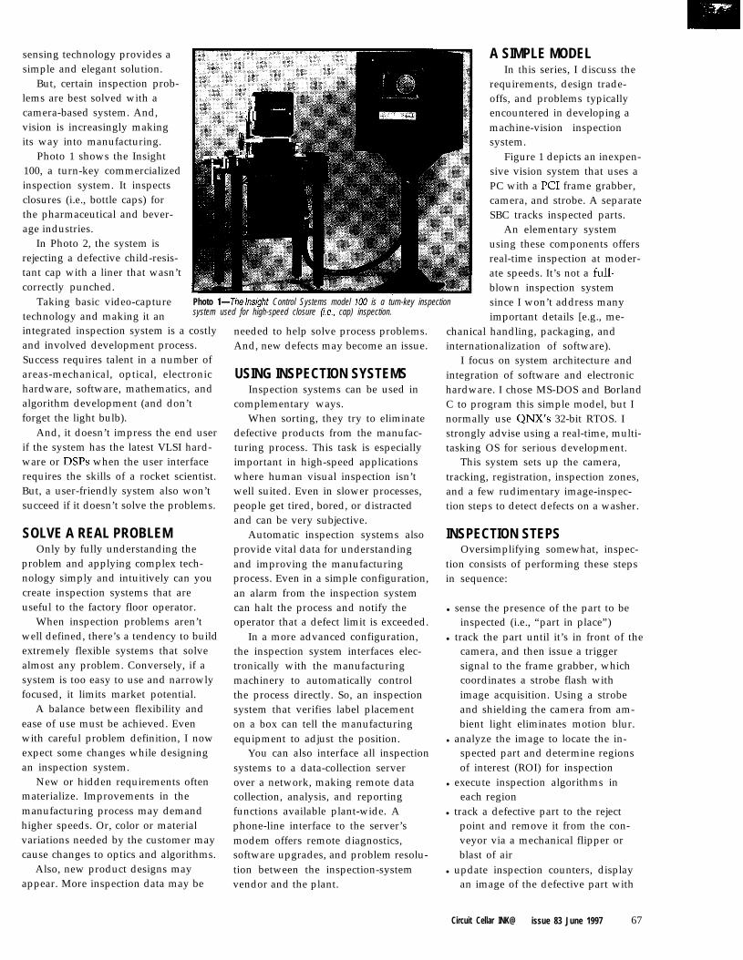
sensing technology provides asimple and elegant solution.
But, certain inspection prob-lems are best solved with acamera-based system. And,vision is increasingly makingits way into manufacturing.
Photo 1 shows the Insight100, a turn-key commercializedinspection system. It inspectsclosures (i.e., bottle caps) forthe pharmaceutical and bever-age industries.
In Photo 2, the system isrejecting a defective child-resis-tant cap with a liner that wasn’tcorrectly punched.
Taking basic video-capturetechnology and making it an system used for high-speed closure (i.e., cap) inspection.
integrated inspection system is a costlyand involved development process.Success requires talent in a number ofareas-mechanical, optical, electronichardware, software, mathematics, andalgorithm development (and don’tforget the light bulb).
needed to help solve process problems.And, new defects may become an issue.
USING INSPECTION SYSTEMSInspection systems can be used in
complementary ways.
And, it doesn’t impress the end userif the system has the latest VLSI hard-ware or DSPs when the user interfacerequires the skills of a rocket scientist.But, a user-friendly system also won’tsucceed if it doesn’t solve the problems.
When sorting, they try to eliminatedefective products from the manufac-turing process. This task is especiallyimportant in high-speed applicationswhere human visual inspection isn’twell suited. Even in slower processes,people get tired, bored, or distractedand can be very subjective.
SOLVE A REAL PROBLEMOnly by fully understanding the
problem and applying complex tech-nology simply and intuitively can youcreate inspection systems that areuseful to the factory floor operator.
When inspection problems aren’twell defined, there’s a tendency to buildextremely flexible systems that solvealmost any problem. Conversely, if asystem is too easy to use and narrowlyfocused, it limits market potential.
Automatic inspection systems alsoprovide vital data for understandingand improving the manufacturingprocess. Even in a simple configuration,an alarm from the inspection systemcan halt the process and notify theoperator that a defect limit is exceeded.
A balance between flexibility andease of use must be achieved. Evenwith careful problem definition, I nowexpect some changes while designingan inspection system.
In a more advanced configuration,the inspection system interfaces elec-tronically with the manufacturingmachinery to automatically controlthe process directly. So, an inspectionsystem that verifies label placementon a box can tell the manufacturingequipment to adjust the position.
New or hidden requirements oftenmaterialize. Improvements in themanufacturing process may demandhigher speeds. Or, color or materialvariations needed by the customer maycause changes to optics and algorithms.
Also, new product designs mayappear. More inspection data may be
You can also interface all inspectionsystems to a data-collection serverover a network, making remote datacollection, analysis, and reportingfunctions available plant-wide. Aphone-line interface to the server’smodem offers remote diagnostics,software upgrades, and problem resolu-tion between the inspection-systemvendor and the plant.
A SIMPLE MODEL
Photo l--The /might Control Systems model 100 is a turn-key inspection
Figure 1 depicts an inexpen-sive vision system that uses aPC with a PC1 frame grabber,camera, and strobe. A separateSBC tracks inspected parts.
An elementary systemusing these components offersreal-time inspection at moder-ate speeds. It’s not a full-blown inspection systemsince I won’t address manyimportant details [e.g., me-
chanical handling, packaging, andinternationalization of software).
I focus on system architecture andintegration of software and electronichardware. I chose MS-DOS and BorlandC to program this simple model, but Inormally use QNX’s 32-bit RTOS. Istrongly advise using a real-time, multi-tasking OS for serious development.
This system sets up the camera,tracking, registration, inspection zones,and a few rudimentary image-inspec-tion steps to detect defects on a washer.
In this series, I discuss therequirements, design trade-offs, and problems typicallyencountered in developing amachine-vision inspectionsystem.
INSPECTION STEPSOversimplifying somewhat, inspec-
tion consists of performing these stepsin sequence:
l sense the presence of the part to beinspected (i.e., “part in place”)
l track the part until it’s in front of thecamera, and then issue a triggersignal to the frame grabber, whichcoordinates a strobe flash withimage acquisition. Using a strobeand shielding the camera from am-bient light eliminates motion blur.
l analyze the image to locate the in-spected part and determine regionsof interest (ROI) for inspection
l execute inspection algorithms ineach region
l track a defective part to the rejectpoint and remove it from the con-veyor via a mechanical flipper orblast of air
l update inspection counters, displayan image of the defective part with
Circuit Cellar INK@ issue 83 June 1997 67
the defects noted, and update pro-cess-control interfaces
Most steps must operate asynchro-nously with respect to the others. Forfull performance, acquisition, process-ing, and display must be able to over-lap in time.
As for software, this description isjust the tip of the iceberg. About 70%of the software goes into developing aninterface that enables the user to easilyconfigure and maintain the system.
SOFTWARE REQUIREMENTSA number of software modules
should be included in an inspectionsystem. Let’s discuss each of them.
Camera setup offers a user interfaceto camera and frame-grabber controls(e.g., gain, reference values, digitalfiltering, etc.). You should be able toacquire images as they pass in front ofthe camera or continually acquire im-ages of a static part by flashing a strobeat a constant rate (autostrobe mode).
A tracking-setup module lets theuser set the correct timing for imageacquisition and rejection. This menumust be fully interactive so the usercan tell when the image acquisitionand reject timing is right.
By differentiating its features frombackground clutter, registration setuptrains the system how to locate thepart and find inspection regions relativeto the registration point(s).
Inspection setup lets the user estab-lish sensitivity levels for each inspec-tion algorithm. It must be interactive,showing pass/fail status on a test image.
Job management provides storagefor sets of set-up parameters related toa certain product type. Image file man-agement loads and stores filed images.
Run-time inspection setup lets theuser fine-tune inspection sensitivitieswhile the machine inspects parts on-line. The run-time screen displays a setof counters and computations showinginspection speed, number of inspectionsand rejects, failure rate, and a break-down of failures by each inspectiontest.
This screen should support severalviews of inspected parts. Viewing eachpart as it goes by is of limited use. Theimages update too fast. However, dis-
68 Issue 83 June 1997 Circuit Cellar INK@
play mode should be supported as itcan indicate whether the system failsto reject defective parts.
A more useful display mode-freezeon reject-updates the display whenparts are rejected. The ability to onlyview rejects provides important processinformation and is a valuable tool fordetecting false rejects (something thatshould have passed inspection).
and 5 12 x 480 pixels, with 8 bits perpixel to allow 256 shades of gray. At600 ppm using 5 12 x 480 resolution,2.5 MBps of bandwidth is used per fullimage operation.
Photo 3 shows the run-time screenfor the Insight 100 running in 256 x 240resolution. In display all rejects mode,the system displays a beverage cap witha break in the seal area (i.e., a nonfillor void] caused by uneven distributionof the liner material.
In the past, standard computer busesweren’t able to handle this load. Mostmachine-vision manufacturers designedspecial hardware with dedicated imagebuses, but they were typically large,proprietary, and expensive.
A more advanced method of freezeon reject lets the user freeze on onespecific inspection step. For instance,the option can be selected to only viewrejects when the nonfill tool fails.
In recent years, more vision systemshave been available commercially, andcosts decreased as systems migrated toPCs. Newer buses (e.g., PCI) are fast,but they still fall short for heavy-dutyvision applications unless the load isdivided carefully among several pro-cessing components.
Finally, the software may requireinternationalization. If you’re design-ing a commercial inspection system, itmust support the local language. I makesystems bilingual, so two languages areloaded into the software at startup-one for the plant and the other for fieldservice technicians.
PC1 transfer rates vary between PCmanufacturers, so be careful if youdepend solely on PC1 bandwidth forsystem performance. Total bandwidthis not a sufficient metric. Instead, theevaluation must consider simulta-neous availability of bandwidth foracquisition, processing, and display.
VISION-SYSTEM ARCHITECTURESSeveral types of systems are avail-
able in the PC-based vision market.STARVING FOR BANDWIDTH
One of the biggest problems inmachine vision is having enough band-width for acquiring, processing, anddisplaying images in real time. Ideally,the system handles all three taskssimultaneously while tracking parts,managing user interaction, and updat-ing process-control interfaces.
A PC and frame-grabber system ismainly suitable where inspection ratesare low or the processing requirementis light. Some frame grabbers haveonboard caching and enough intelli-gence to capture an image from a hard-ware trigger asynchronously withouthost CPU interaction.
Although line speeds varyacross industries, it’s commonfor systems I design to operate inthe ranges of 400-2500 parts perminute (ppm). When inspectingat 600 ppm, there are -100 msbetween parts.
This speed is approximatesince parts may not be evenlyspaced, causing inspection speedsto burst occasionally. The systemneeds enough extra performancecapacity to handle bursts with-out missing inspections or goingsouth.
Frequently used image resolu-tions for high-speed industrialinspection are 256 x 240 pixels
Photo 2-Defective closures must be eliminated from production.The cap being rejected has a flaw in the cut of the liner material.

Photo 3-The run-time screen should show process statistics, as well as enabling the operator to select the displaymode, c/ear production counters, and modify the inspection sensitivity while the system continues to inspect.
If more than one camera is used,caching and asynchronous operationare critical. Except for very slow-speedapplications, the only suitable PC busis a high-speed one like PCI.
In PCs with coprocessors (e.g., DSP,RISC, CISC) and frame grabbers, someof the newer processors (e.g., the TI‘C80) are extremely powerful pixelbangers. But, you may have to writehighly optimized assembly code.
This multiprocessing architectureclears up some bottlenecks, but it cankeep you reaching for the aspirin. Co-ordinating processes across multipleprocessors and designing in robust errorrecovery is complicated. Processordissimilarities between the host andcoprocessor (e.g., byte ordering anddata alignment) need to be considered.
A PC with special hardware and aframe grabber normally offers a limitedset of very fast image-processing func-tions. Additional analysis or processingmay be necessary on the host PC. Ahigh-speed bus to the special hardwareand frame buffers is a big advantage.
The PC, running under an RTOS,serves as the system controller, han-dling the user interface and the commlink between the tracking and process-ing sections. A high-speed bus con-nects the PC and vision processors.
LIGHTING AND OPTICSFinding the right lighting technique
is the first step in evaluating the use ofmachine vision in any application.Most real-time image-analysis softwarerequires the inspected part to be illumi-nated so that any defects cause a con-trast, color, or other change.
In more difficult inspections, morethan one lighting technique is neededfor 100% defect detection. Defectsvisible with one technique disappearwith another. Look for a more general-ized lighting technique or use multiplecameras and optical assemblies.
The topic of lighting and optics ishuge. Cognex’s minicourse proffers afundamental exposure to the subjectand useful course notes. In fact, theyoffer an excellent one-week course in
machine-vision fundamentals for engi-neers with a strong grasp of C.
Three types of light sources arecommonly used-LEDs, strobes, andvarious constant light sources. I covertheir pros and cons in Part 3. My ex-ample system uses a commercial Xe-non strobe with a fiber-optic light ringand diffuser.
CAMERASCamera technology is advancing
rapidly, resulting in a wide range ofnew capabilities in a smarter, smaller,and faster package. They’re also con-fusing, due to a lack of standardizationboth in function and terminology.
A few years ago, I found myselfrefereeing between my camera andframe-grabber suppliers. After thediscussion circled a few times, it be-came apparent that we were sufferingthe Tower of Babel syndrome.
They were arguing over a subtletiming issue related to even and oddfields of video. But, one supplier num-bered the fields 0 and 1, while the otherused 1 and 2. Once terminology wasresolved, the technical issues were, too.
For very high-speed applications, usea camera with a high-speed random-reset capability. Be careful you under-stand the timing and side effects whenusing special camera modes.
Some cameras accumulate ambientlight while waiting for a reset pulse,which can cause blooming in the im-age. Other cameras advertising random-reset capability require a considerabletime delay to reset.
Of course, I’m still lookingfor the ideal vision engine thatbalances hardware- and soft-ware-based processing. Sensor p,p TWer PC and PCI bus
ASICs can be used for image-w 68H,., , sBc
- Frame Grabber Camera
processing functions requiringRS-232
&* -+-w
fast, repetitive neighborhoodprocessing (e.g., histograms,
Encoder
convolutions, morphology, etc.). -i%
A high-speed processor per-forms intelligent postprocessing Figure l-Here, you see the major components and interconnections in a
to arrive at a pass/fail decision. simple inspection system.
An inspection system’s displayoften poses difficult technical issues,since it must display both images andthe user interface.
You could use two moni-tors-one for images and theother for the user interface.However, the system packagingtends to become too bulky, andreal estate is often at a pre-mium.
Using two small monitorssounds good until you checkprices. If you need multiplecameras later, do you add amonitor for each?
DISPLAY
70 Issue 83 June 1997 Circuit Cellar INK@

“We’re impressed by thedocumentation and the readability
of the code. ‘I - M. Ryan
“We are very pleased with theGeneralSo/hvare BIOS and look
forward to working with you to bringour product to market. ” - R. Levaro
Embedded BIOS is well-structuredand documented, and technicalsuppoti at General Sofrwore is
erceUen~ -J. Toivanen
‘lam sure we made the rightdecision to buy our BIOS fromGeneral Sojiware. ” - I! Fillon
“‘Embedded BIOS is really &&tfor embedded PC designs.
You were absolutely right ” - J Jesse
Why You Should Choose Embedded BIOS, Toom BIOS, DOS, Flash Disk With One low RoyaltyQ Instant Boot, Console Redirection, & Much More
u Expert Support with Guaranteed Response Timem We Work Closely With Acer, AMD, Intel, & RadiSys
to Deliver you a Proven, Tested, Feature-Packed BIDSa Millions of Units Already licensed
BIOS Adaptation Kit Includes:Q Complete Source Code0 Binary Configuration Program
0 Quick Start + Over 600 Pages 01 Printed Documentation
General Software, Inc.3 2 0 - 108th Ave. N.E., Suite 400 * Bellevue. WA 98004Te l : 206 .454 .5755 . Fax : 206 .454 .5744 - Sa les : 800 .850 .5755http://www.gensw.com/generol - E-Mai l : [email protected]
inlith Cimetrics’ g-Bit PLAN you can link together up to 250 of the most popular 8- and16-bit microcontrollers (8051,8OC196,80C186EB/EC, 68HC1i168HC16, 68332, IPICI 6C74).
The Q-Bit &AN is:t Fast- A high speed (62.5k baud) multidrop
master/ slave RS-485 network
t Flexilble- Compatible with yourmicrocontrollers
F Reliaible- Robust 16-bit CRC and sequencenumber error checking
. Enicient- Low microcontroller resourcerequirements (uses your chip’s built-in serialPod)
b Friendly- Simple-to-use C and assemblylanguage software libraries, with demonstrationprograms
b Complete- Includes network software,network monitor, and RS-485 hardware
. S&&r/-The 9-Bii PLAN is an asynchronousadaptation of IEEE 1118
55 Temple Place l Boston, MA 02111-1300 l Ph 617.350.7550 l Fx 617.350.7552#140I -72 Issue 83 June 1997 Circuit Cellar INV
A dedicated image monitor mayalso have a downside if the visionhardware doesn’t provide a nonde-structive graphics overlay. You thenend up drawing directly to the imagebuffer, which is a disadvantage if youneed to reuse that image. Of course,software may repair screen damage.
Single-monitor displays also posesome design challenges, since theimage and user interface share a screen.
Some vision systems have directoverlays over the image. Others use adedicated window for image displayand arrange the user interface around it.In windowed systems, though, thedisplay must run in very high-resolu-tion graphics mode, requiring a largemonitor.
Whatever technology you choose, itshould display images with graphicsnotations to mark defects in real timewith little performance penalty. Other-wise, you’ll have to make significantcompromises in system performanceto work around the deficiency.
And, avoid display methods thatsubsample the inspected image. Smalldefects can be hidden, leading theoperator to incorrectly assume that thesystem has a problem with false re-jects.
Now that you have the background,you’re ready for Part 2. I’ll cover acomplete tracking system using aMotorola 68HCll SBC. q
Hugh Anglin is a systems engineerwith experience in real-time and em-bedded systems, process control, andmachine vision. You may reach himby E-mail at [email protected] or by phone at (918) 3422248.
Lighting and Optics WorkbookCognex Corp.One Vision Dr.Natick, MA 01760-2059(508) 650-3105Fax: (508) 650-3332
422 Very Useful423 Moderately Useful424 Not Useful

It Can’t BeA Robot
Jeff Bachiochi JUST A TOY
Part 1: There areNo Arms and Legs! ehere do you think
you’re going?”“Be-dop be-doop.”
“Well, I’m not going thatway. It’s too rocky. What makes youthink there are any settlements thatway anyhow!”
“Thwerp, biddy biddy ba-werp.”“Don’t get technical with me. I’ve
had just about enough of you. Go thatway. You’ll be sandlogged within aday, you nearsighted scrap pile.”
It’s not the kind of conversation thatcomes to mind when we think of com-puters communicating. It’s more likean act from the Comedy Club circuitrather than from a protocol (C3PO) andastromech droid (R2D2) lost in theJundland desert on Tatooine.
I cheer George Lucas and those whopioneer the existence of robotics fromGort through Data. Our technologymay not be on the same plane as our
dreams and fantasies, but those dreamsand fantasies drive technology forward.
One reason robotics is so popular isbecause it touches on so many fields-motion, sensing, power, and intelli-gence. Improvement in one area candramatically alter other fields.
Don’t tell my wife, Beverly, but Ilike flipping through catalogs. Not theWalter Drake or Harriet Carter stuffshe reads, but good stuff like Mondo-tronics and Edmund Scientific.
I keep my eyes peeled for unusualitems. Tons of robot kits saturate thesecatalogs. Thing is, most kits only per-form a specific function: follow a line,move toward light, hug the wall, avoidfalling off a table top. As teaching tools,these kits have carved out quite a niche.
Toys, however, are for fun. Althoughthere’s some truth to the saying “thebigger the boy, the bigger the toy,” Ibelieve the toy’s cost is not what makesit delightful.
Tamiya, a Japanese company, hasan impressive line of motorized toyvehicles. I was a bit apprehensive aboutspending $40 when I had no idea of itsquality. I was even more frustrated tolearn the kit was discontinued.
Scurrying back through the catalogs,I found an alternative from Mondo-tronics. Photo 1 shows the parts of thePower Shovel/Dozer kit.
What’s so impressive about it? Thethree electric motors have preassem-
Photo 1-Tarniya supplies a co//age of park made from wood, metal, plastic, rubber-whatever firs the job.
74 Issue 83 June 1997 Circuit Cellar INK@

bled gear boxes giving a good mix oftorque and speed. The independentlycontrolled rubber tracks make moving
By rotating the tracks in oppositedirections, you get a tight turning ra-
over small obstacles a breeze.
dius. Using only two 1.5-V D cells, yougain motor control through joystick-type switches at the end of a 3’ umbili-cal cord. The major holes are predrilled.It would be easy to assemble-even foran 8-year-old.
EDUCATIONAL PLATFORMSome might suggest I’m copping out.
Surely, I should design it from scratch.Essentially, I agree, but I want to
spend the time I have controlling thebeast, not fabricating one. So, I’m goingto use a known quantity and add mo-tion, sensing, and maybe even a weebit of intelligence.
Constructing the Dozer took lessthan 2 h. After taking it on a few spins,I dug out the multimeter and measuredthe current draw of each motor.
I measured -0.5-A continuous run-ning current with peaks of -0.75 A.Using the seat-of-the-pants 2x rule, Isearched for motor drivers that couldhandle 1 A continuous. I wanted theparts to be accessible.
National’s LM18293 jumped out ofthe databook, and it’s available from
This single device has quad push-pull drivers. It can be used to form two
Digi-Key. It was on National’s Web
H-bridges, one for either motorized
page, so I knew it wasn’t on death row.
tread. With an H-bridge, the motor canrun in both directions without needinga bipolar supply. The only thing miss-ing was internal protection diodes.
Figure 1 illustrates how I used the‘18293. Each H-bridge is formed with apair of push-pull amplifiers, each hav-ing two inputs and sharing an enable.
To be configured as an H-bridge, theinputs must be driven by opposinglogic. If the inputs are both driven highor low, there’s no potential across themotor. An ‘04 inverter kept the inputsopposed.
across the motor. Not terribly efficient,but at $5, it’s at least cost effective.
This device uses transistor junctions.The more expensive parts (e.g., an
The motor drive IC was shown tohave webbed legs on pins 415 and 12/13,but the parts I received didn’t havethem. These ground pins are beefed upto also give heatsinking for the chip.
The drop across each driver is about1.5 V, so I needed -5 V just to get 1.5
LMD18200) use MOSFETs so the dropsare considerably less. But, they are asingle H-bridge device and cost -$20. Ifyou substitute a pair of these, they’llcost as much as the motorized platform.
MOTIONTo control the motor driver, I used
a micro. To keep costs low and theprogramming environment friendly, Iused Pi&tic 1. The reprogrammableflash memory let me change BASIC (orassembler) programs easily-my formof experimental nirvana.
I’ve used PicStics a lot lately. It’s afriendly device for those who alwayswanted to play around with micros butdidn’t dare to, given entry-level costs.
Whenever possible, I define theupper two bits of the I/O port as serialoutput (bit 7) and serial input (bit 6),even if the project doesn’t requireserial communication of any kind.
deep within the bowels of a project.The open-collector mode of the
serial communications protocol per-mits simple networking. The se r i n
It’s a useful debugging feature, andit enables me to use the same 5-wirenetworking connection on all my pro-jects. The same connections can thenreprogram the micro even while buried
Figure l--This schematic outlines the controls for left andright tread motors. Also note the solid-stafe encoders Irep/aced with microswitches.
Circuit Cellar INK@ Issue 83 June 1997 7.5

statement ignores all communicationuntil a particular character sequence isrecognized, so you can keep othermicros hanging on the same bus frominterfering with private conversations.
I use the capital letter M as a singleaddressing character followed by oneof four 2-byte commands-forward( Fx), backward (Bx), left turn [Lx), andright turn (Rx), where x=1-255 counts(0 being continuous). A count is aspecific unit of distance measurement.
The only difference between mov-ing forward/backward and turning isthat the treads move in opposite direc-tions instead of moving in the samedirection. The base rotates about itscenter in a tight radius, making theplatform highly maneuverable.
SYNCRONICITYThe twin DC motors that indepen-
dently move the left and right treadsrun at different speeds depending onfriction and load presented to eachmotor. Therefore, starting and stoppingthem together doesn’t assure that bothtreads move the same distance.
Although the treads can indepen-dently slip in relation to one another,it’s helpful to keep the dual drives insync. To do this, you track the distancetraveled by each drive train, perhaps byusing shaft encoders. However, thisvehicle has components that lendthemselves to tracking distance.
The front wheels have three equallyspaced holes that can be used to countwheel rotation (distance) by one-thirdor about a linear inch between holerotations. The rear wheels have teeththat engage the plastic track. The gearteeth are spaced about every 0.25” andprovide better resolution.
Remember when floppy disk driveswere open framed and you could seetheir inner workings? The head move-ment was usually initialized to trackzero by moving the head back and forthand sensing when a plastic vane on thehead carriage slipped into an opticalinterrupter. This interrupter was madefrom an IR transmitter/receiver pairaimed at one another across a short gap.
The same IR pair can be positionedover the rear wheel’s teeth so the rotat-ing teeth break the IR beam. By track-ing the number of times the beam is
Listing l--This Pi&tic 1 BAXprogram queries for a motor command (f, B, R, L) and a count. The let7 andright tread motors will then operate appropriately for the desiredcommand.
symbol fwrd = 1 : symbol bwrd = 0 : symbol go = 1symbol halt = o : symbol open = 1 : symbol closed = 0symbol ldir = pin0 : symbol len = pin1 : symbol lsen = pin2symbol rdir = pin3 : symbol ren = pin4 : symbol rsen = pin5symbol cnt = b0 : symbol mode = bl : symbol lmode = b2symbol rmode = b3 : symbol emstop = b4
start: poke $81,$7f
startl:
pinO=O : pinl=O : pin3=0 : pin4=0 ’dirO=l : dirl=l : dirZ=Odir3=1 : dir4=1 : dir5=0ldir=fwrd : len=goif lsen=open then start.1len=halt : rdir=fwrd : ren=go ’
start2:
loop:
F:
B:
R:
L:
loopl:
if rsen=l then start2ren=haltserin 6,n9600,("M"),bl,#bOSEROUT 7,N9600,("M",B1,~~B0,13,10) ’if bl=$46 or bl=$66 then Fif b1=$42 or b1=$62 then Bif bl=$52 or bl=$72 then Rif bl=$4C or bl=$6C then Lgot0 loopldir=fwrd : rdir=fwrdgot0 loop1ldir=bwrd : rdir=bwrdgot0 loop1ldir=fwrd : rdir=bwrdgot0 loop1ldir=bwrd : rdir=fwrdgot0 loop1lmode=O : rmode=O ’ clear Itif cnt=O then loop3 ’ if countif cnt<>l then loop2 ’ if count
loop2:loop3:loop4:
got0 loop ' else watch for a cmdcnt=cnt-1 ’ reduce the countlen=go : ren=go ’ enable both treadspeek BO5,emstop ’ chk emerg stop inputemstop = emstop & $10if emstop = 0 then allstop ’ if low go stopif lmode>l and rmode>l then loop1 ’ if both treads closed
if len=go then Ll
Ll:
loop5:
Rl:
got0 loop5if lsen=lmode then loop5 ’pause 1lmode=lmode+lif Imode< then loop5 ’len=haltif ren=go then Rlgot0 loop4if rsen=rmode then loop4 ’pause 1rmode=rmode+lif rmode<Z then loop4 ’ren=haltgot0 loop4
logic 0 on pins 0,1,3,4outputs 0,l input 2outputs 3,4 input 5enable it tread = fwdloop til It sensor = closeddisable It treadenable rtloop tildisable rwatch forrespond wbranch tobranch tobranch tobranch to
tread = fwdt sensor = closedtread
cmdth cmdfwd if 'F' or 'f'bwd if 'B' or 'b'rt if 'R' or 'r'It if 'L' or '1'
else watch tor a cmdboth treads fwd
both treads bwd
It tread fwdrt tread bwdIt tread bwdrt tread fwdand rt mode= 0 skip decrement<> 1 go on
allstop:len=halt : ren=halt ’got0 loop
do next countif It tread enabled, chk It snrelse chk rtif It snr unchanged, chk rtelse wait 1 msincrement modeif mode<2 go chk rtelse disable It treadif rt tread enabled, chk rt snrelse chk emerg stopif rt snr unchanged, chk emerg stopelse wait 1 msincrement modeif mode<2, chk emerg stopelse disable rt treadcheck emerg stopdisable both treadswatch for a cmd
broken, we can calculate the distance this method, I would have to paint thethe tread moves. gear’s teeth. But, I was worried about
Now, this all sounds good on paper, the paint scratching off, so I discardedbut I ran into a little snag. I couldn’t get the IR sensors for a mechanical switch.the IR sensors to sense the gear teeth. I picked up a couple microswitches
The orange plastic used in the gears with levers. Not only did the lever givepassed IR like it wasn’t there. To use a mechanical advantage, but an idler
76 Issue 83 June 1997 Circuit Cellar INK@

nstall
rmode-rmode+l
1 mode=0 len=O rmode=O ren=O
dec cntll3kl
En=1
Figure 2--This flowchad lets youtrace how the leff and right motorsoperate for the four commands.
wheel at the lever’s end fit perfectly ceived before the serial routine pro-between the gears’ teeth. ceeds.
The switch has about 1 ms of con- Two characters are expected aftertact bounce. A bit of external circuitry the qualified-the command and thecould cure this problem (a fast microwould see the bounce as multiplecounts). Instead, my code pauses briefly
Control is simplest if you enablethe motors and keep them in step by
whenever the switch changes states.
monitoring the left and right treadcounts. If the counts don’t stay equal,it temporarily disables one motor.
To move straight, the micro enablesboth motors for a specific number ofcounts. To stop it before it finishes amove, use an emergency stop input.
FLOW CARTOGRAPHYAs Figure 2 shows, the software is
simple, using only about 60 commands.Once the processor is initialized, itjogs the left and right treads, settingthe position sensors to a known state.
It then waits for serial input. M (formotor) is a qualifier that must be re-
count. Based on the command, the leftand right direction flags (1 d i r and
Now, we’re ready to move. If thecount received with the command is 0,
r d i r ) are set to 1 for forward and 0 for
then counter decrementing is avoided
reverse movement.
and the control loop (moving each treadone sensor count) executes continu-ously until the emergency stop inputis pulled low. The control loop is thenexited, and it waits for serial input.
If the count anything other than 0,it decrements each time through thecontrol loop until it reaches 1. At thattime, the loop is again exited to awaitanother command.
The control loop enables the motordrivers for both treads. It then entersan inner loop that alternately checkseach tread’s sensors for changes ofstate.
When each tread completes a moveor step, it is disabled until the othertread catches up. (I hope this will keepthe Dozer from veering off course.]Once both treads move, the loop exitsand the count is decremented.
SIMPLY BASICIt shouldn’t be tough to convince
you just how easily this platform isprogrammed. Take a look at Listing 1.
It takes -100 counts to do a 360”turn. The commands can come fromyour keyboard via terminal software.
But, what now? The umbilical cord.Next month, I cut the apron strings.
“Klatu Barata Nikto!” q
[eff Bachiochi (pronounced “BAH-key-AH-key”) is an electrical engineer onCircuit Cellar INK’s engineering staff.His background includes productdesign and manufacturing. He may bereached at jeff. [email protected].
For more information on National’sLM18293, check their Web site(www.national.com).
Motorized Power Shovel/DozerTamiya America, Inc.2 OrionAliso Viejo, CA 92656(714) 362-2240Fax: (714) 362-2250
LM18293 Quad push-pull1-A driversDigi-Key Corp.701 Brooks Ave. SThief Falls, MN 56701-0677(218) 681-6674Fax: (218) 681-3380
PicStic 1Micromint, Inc.4 Park St.Vernon, CT 06066(860) 871-6170Fax: (860) 872-2204www.micromint.com
425 Very Useful426 Moderately Useful427 Not Useful
Circuit Cellar INK@ Issue 93 June 1997 77

Tom Cantrell SHADES OF MICROCODE
High-Velocity DSP
ompelled by themarch of silicon
integration, computerarchitects are doing their
best to find a way through a maze ofrocks and hard places.
Instruction-level parallelism-howmuch there is, how to find it, and howto exploit it-is a key area of interest.Another is the chip-level equivalent ofconvergence, blurring the distinctionbetween ICs processing data and thoseprocessing signals (see M.R. Smith’s“To DSP Or Not To DSP,” INK 28).
For the most part, microprocessorgurus have had a pretty easy go of it.They’ve gotten away with brute forcing(thanks to nearly free transistors) moremileage out of old mainframe ideas.The modern generation of pipelined,superscalar, speculative semiSIMDCPUs is the result.
But now, other than boosting clockrate and on-chip cache/memory size,it’s getting tough to squeeze moreMIPS out of evolutionary designs.Pressure is building for an architecturalparadigm shift.
Meanwhile, as computers take onthe challenges of multimedia, design-ers look for solutions with the optimalcombination of data and signal pro-cessing. Perhaps the time is right totake a closer look at one of the newerconcepts-VLIW (Very Long Instruc-tion Word).
A number of chips have toyed withthe idea, but so far, it’s remained littlemore than a lab curiosity. Now, theconcept is getting a big push from TIin the form of their new ‘Cbx series ofDSPs featuring a VLIW architecturethey call VelociTI.
Like most ideas in computing, VLIWisn’t brand new. It’s just newer thanmost of the rest.
The original concepts harken backto the days of microcode (rememberhow CISCs used to work?). The chal-lenge is to transform vertical microcodeinto a faster horizontal format withseparate fields for each functional unit.
Hennessy and Patterson [l] relatethe early history of VLIW as embodiedin research and commercial machinessuch as those offered by Floating PointSystems, Cydrome, Multiflow, andcompanies you’ve likely never heard of.
The reason you’ve never heard ofthem is that these machines, and other’80s vintage CPUs with VLIW-esquefeatures (e.g., the Intel ‘860 and experi-mental MIPS prototypes), never ob-tained much commercial success.
Some argue this proves the VLIWconcept is just another example of abad idea whose time has come, but Isuspect it’s not that simple. Perhaps acombination of at-the-time immatureand constrained technology along withthe end of the Cold War (sapping themarket for performance-at-any-pricecrunchers) was more to blame.
While main CPU architects remainskeptical, the VLIW approach has foundfavor in the niche of chips known asmultimedia accelerators from the likesof Chromatic and Trimedia. Thoughthe jury is still out, these chips seemwell on their way to rehabilitating theVLIW concept. Needless to say, thelatest blessing from TI is both signifi-cant and timely.
MISSION IMPOSSIBLEThat old joke about RISC standing
for Relegate the Impossible Stuff to theCompiler might better be said aboutVLIW.
From high altitude, the problem israther simple. The goal: execute asmany instructions per clock as possible.
78 Issue 83 June 1997 Circuit Cellar INK@
So, CPU operations are scheduled tofully exploit opportunities for paralleloperation.
Unfortunately, a variety of depen-dencies and constraints get in the way.For instance, you can’t read a variablebefore it’s written, and you can’t de-mand n functional units when the chipo n l y h a s n - 1 .
How best to schedule instructionssubject to these constraints is wherethe arguments arise. Conventionalsuperscalar CPU wisdom calls for abunch of complex, ugly hardware todynamically examine and reorderinstructions at runtime. The good newsis such a chip can handle old binaries,although a recompile is usually neces-sary for top performance.
By contrast, VLIWs rely on static, orcompile-time, scheduling to organizeinstructions most efficiently ahead oftime. Instructions that can execute inparallel are lined up arm to arm for
digestion by the multiple functionalunits in one big gulp.
Reasonable observers can disagreeon whether scheduling dynamically(hardware) or statically (compiler)makes more sense. For instance, run-time hardware can adapt to conditionalbranch behavior, but a static schememust commit one way or the other.
On the other hand, dynamic sched-uling can only deal with a small win-dow of instructions. Static schedulingcan examine the entire program. Run-time optimization incurs a siliconpenalty for each chip shipped, whereasstatic schemes only pay a compile-time penalty, presuming such a com-plex compiler can get beyond beta.
In fact, the overall trend seems to beto combine the two schemes. By mak-ing both the chip and compiler smarter,we can let each do what it does best.
One key question keeps popping up.Just how much instruction-level paral-
lelism (ILP) is to be found? The answer:It depends.
For example, Hennessy and Patter-son examined traces of SPEC92 bench-marks and found large amounts of ILP(17.9-150.1 instructions per cycle).However, since this is based on hind-sight (actual program traces), it modelsa perfect machine with its infiniteresources (registers and function units).
It has foolproof branch predictionand a full program-size reorder buffer.Also, it has no aliases, referring to thesituation, as with a C pointer, whereit’s next to impossible to determine ifa data dependency exists.
Even the most java-jolted architectknows such a machine is a look-aheadpipedream. Hennessy and Pattersonperform a similar analysis with a realCPU (PowerPC 620). Although it’stheoretically capable of issuing 4 in-structions per cycle, it barely averages1.3. Ouch!
Figure l--The radical architecfure of the ‘C6201 represents a major blessing of-and commitment to-the K/W concept by TI
Circuit Cellar INK@ Issue 83 June 1997 7 9
However, one key point (and hope)to note is that different kinds of pro-grams exhibit more or less ILP. Inparticular, vector loops (e.g., vectoradd, dot product, etc.) are relativelymore parallelizable, and such routinesare at the core of signal processing.
I’ve spent a lot of time up frontlooking at the big picture in the hopeof making the motivation behind VLIWa little easier to understand. Needlessto say, the TI chips aren’t your father’sCPU.
V8 PUNCH“There’s no substitute for cubic
inches” is a hot-rodder maxim thatapplies well to the first chip in the ‘Cbxseries-the 32OC6201. The chip com-bines a whopping 8 functional unitswith 1 Mb of on-chip zero-wait-stateSRAM and a bunch of glue logic, allrunning at up to 200 MHz (see Figure 1).
Featuring the silicon equivalent ofmultiport fuel injection, each func-tional unit gets its own 32-bit fetchbus. It makes for a 256-bit “instruc-tion,” which is what the VL in VLIWis all about.
The on-chip SRAM is split in half,with 2k 256-bit instructions joined by16 K x 32 data RAM. The instructionmemory can be reconfigured to operateas a direct-mapped cache.
SIMD-like partitioning of the data-memory interface enables simultaneoustransactions to different banks. Regis-ters and off-chip data memory are all
Register File A
Registers used forcircular addressina
Registers testedfor condition
I Registers used with I I I I15-bit offset addressing
Figure 2--Each cluster has a complement of 16 Kx 32-bit registers. A// regisfers are genera/ purpose! !houghcertain ones suppoP alternative functions, including circular addressing, long branch offsets, and cond/bona/execution.
Note that switching the program branches based on PSW flags is com-RAM from memory to cache mode pletely discarded.invalidates the cache. However, it is Instead, the CPU has conditionalpossible to freeze the cache anytime, execution for every instruction basedlocking the contents for fast and deter- on the contents (zero or nonzero) ofministic access.
Much as a V8 is conceptually twostraight-4s stuck together, the C6201is actually a pair of I28bit VLIWs.Each has four function units, 16 K x32-bit registers, and a 32-bit data bus.
Like a crankshaft, cross paths linkclusters, enabling function units on oneside to access registers on the other.Similarly, a register on one side gener-ates an address for loads/stores on theother.
As shown in Table 1, each functionunit is responsible for part of the in-struction set. It’s an interesting hybridof three-operand load/store RISC spicedup with DSP features.
The latter includes circular address-ing (i.e., software FIFO), saturated math(results top and bottom out, rather thanoverflow), 40-bit calculation headroom[using a pair of registers), and so on.Barrel shifters support a variety of one-
byte, half-word, and word addressable. clock bit field operations, includingIt’s possible to store into the pro- shifts, searches, and extracts.
gram memory 32 bits at a time with Other features not particularlythe STP instruction. But, there’s no related to DSP functions are interest-way [and since it’s RAM, no need) to ing nonetheless. For instance, theload from program memory. traditional concept of conditional
.L Unit .M Unit .S Unit .D Unit
ABS NORM MPY ADD EXT SET ADDADD MPT SMPY ADDK EXTU SHL ADDAANDC M P E Q ::DD
ADD2 MVC* SHR LD memAND MV SHRU LD mem (15-bit offset)**
CMPGT SAT B disp MVK SSHL MVCMPGTU SSUB B IRP* MVKH STP* NEGCMPLT SUB B NRP* NEG SUB ST memCMPLTU SUBC B reg NOT SUB2 ST mem (15bit offset)**LMBD XOR CLR OR XOR SUBMV XOR ZERO SUBANEG ZERO
Table l--The ‘C6201 relies on four types of functional units to handle fhe entire instruction sef. Two such groups(each sometimes referred to as a “cluster”) compose the total of eight function units. Sing/e-asterisk instructions onlyapply to the 52 components, and double asterisks apply to .02.
80 Issue 83 June 1997 Circuit Cellar INK@
certain registers. This works in concertwith CMP instructions that comparetwo source registers and put a 0 or 1 ina destination register accordingly.
Thus, there aren’t any conditionalbranch (B) instructions per se. But likeany other instruction, branches can bemade conditional. Besides the expectedregister and displacement options, theB I R P and B N R P variants act as re-turns from maskable and nonmaskableinterrupts, respectively.
Like some other RISCs (MIPS comesto mind), the ‘C6201 does little inresponse to interrupts except store thereturn address one-level deep on chipand mask further interrupts. Any nest-ing, dynamic priority, or other fancyinterrupt pretensions are left com-pletely up to software.
As you see in Figure 2, other regis-ters play special roles for circular ad-dressing and long (15 vs. 5 bit) offsetaddressing. Circular addressing modeis enabled with a control register thatalso specifies block size (powers of twobetween 2l and 232 bytes).
Subsequently, add and subtractoperations on the affected registers(whether via an explicit ADD and S U Bor a load/store address increment anddecrement) are calculated in a modulomanner (i.e., they wrap around oncethe block size is exceeded).
NOP IN MY BACKYARDTable 2 shows the ‘C6201 “pipe-
line,” though that term is a bit mis-leading.
The front of the pipeline is a single256-bit-wide datapath that grabs fetchpackets from memory. In the middle,the long fetch packet splits into 32-bit

Listing 1 a-A fypical DSP loop wriffen in C translates easily info serial assembler (b). c-0pfimizafion startsby scheduling around resource constraints and filing delay slots. d-The loop is unrolled to hand/e two arrayelements per iferafion and expose more paraallelism. +Final/y, software pipelining packs the entire loop infoone 256-bit K/W insfrucfion. The asterisks show how each unit works on a different iteration of the loop,eliminating dependencies and every sing/e NO/?
a) int dotpcshort aLI, short b[l)Lint sum = 0, i;for (i=O; i<lOO; i++) sum += ali] * b[il;return(sum):
b) MVK .Sl 100, AlZERO .Ll A7
LOOP: LDH .Dl *A4++.A2LDH .Dl *A3++:A5NOP 4MPY .Ml A2,A5,A6NOPADD .Ll A6,A7,A7SUB .Sl Al,l,Al
[All B .s2 LOOPNOP 5
;Branch occurs here
c) MVK .Sl 100, Al
LbOP:ZERO .Ll A7LDH .Dl *A4++.AZ
I I LDH .D2 *B4++:B2SUB .Sl Al,l,Al
[All B .S2 LOOPNOP 2MPY .MlX A2,B2,A6NOPADD .Ll A6,A7,A7
;Branch occurs here
d) MVK .Sl 50,AlI I ZERO .Ll A7i i ZERO .L2 B7LOOP: LDW .Dl *A4++.A2
LDW .D2 *B4++:B2SUB .Sl Al,l,AlB .Sl LOOPNOP 2MPY .MlX AZ,B2,A6MPYH .MZX A2,BZ,B6NOPADD .LlADD .L2; Branch ocADD .LIX
B s2MVK :s1B .s2B .s2ZERO .LlZERO .L2B s2ZERO :LlZERO .L2
A6,A7,A7B6,B7,B7
:curs hereA7,B7,A4
LOOP51,AlLOOPLOOPA7B7LOOPA686
OOP:
ii:;I
B s2 LOOPZERO :Ll A2ZERO .L2 B2ADD .Cl A6,A7,A7ADD L2 B6,B7,B7MPY :MlX A2,B2,A6MPYH .M2X A2,B2,B6
1 ADD .Sl -1.Al.AlI B .s2 L O O P
LDW .Dl *A4++,A2LDW .D2 *B4++,B2; Branch occurs hereADD . LlX A7,B7,A4
set up loop counterzero out accumulatorload ai from memoryload bi from memorydelay slots for LDHai * bidelay slot for MPYsum += (ai * bi)decrement loop counterbranch to loopdelay slots for branch
set up loop counterzero out accumulatorload ai from memoryload bi from memorydecrement loop counterbranch to loopdelay slots for LDHai * bidelay slots for mpysum += (ai * bi)
set up loop counterzero out sum0 accumulatorzero out sum1 accumulatorload ai & ai+l from memoryload bi & bi+l from memorydecrement loop counterbranch to loop
ai * biai+l * bi+l
sum0 += (ai * bi)sum1 += (ai+l * bi+l)
sum = sum0 + Sum1
branch to loopset up loop counter* branch to loop** branch to loopzero out sum0 accumulatorzero out sum1 accumulator*** branch to loopzero out ADD inputzero out ADD input**** branch to loopzero out MPY inputzero out MPY inputsum0 += (ai * bi)sum1 += (ai+l * bi+l)** ai * bi** ai+l * bi+l****** decrement loop counter***** branch to 100~******* Id ai & ai=i fm memory******* Id bi & bi+l fm memory
sum = sum0 + Sum1
execute packets for dispatch to eachfunctional unit.
Each single-stage functional unitthen requires a particular number ofcycles depending on the operation (i.e.,one for simple ALU ops, two for multi-plies, five for loads, six for branches).
Rather than interlocks, the ‘C6201relies on delay slots to handle the varying cycle count in the execution stage.The compiler tries to find useful in-structions to fill the void, but it’s toughto do. Sometimes, the only choice is tokill time with NO Ps. To this end, TIincludes a NOP i/N (n = 1 to 9) instruc-tion to prevent needless duplication.
Along similar lines, concerns aboutVLIW code density have been made.After all, if the machine only delivers“a few” instructions per cycle on realprograms, then there are “8 minus afew” N 0 Ps in baggage. Memory may becheap, but it’s not cheap enough tothrow half or more away.
TI’s solution is to make the leastsignificant bit of each 32.bit instructiona parallel bit. If it’s 1, the next instruc-tion in the fetch packet is added to thecurrent execute packet. If 0, the nextinstruction goes into the followingexecute packet.
All in all, the ‘C6201 goes a longway in placating the N 0 P naysayers.
MOTOR MOUNTSThough the 352-pin ball grid array
(BGA) package may make you fear theworst, the ‘C6201 glue logic prettymuch insulates the system designerfrom the on-chip complexity. Actually,about half the pins are devoted to thedual power supply, comprising 2.5 Vfor internal operation and 3.3 V for I/O.
To date, final production devicepower hasn’t been characterized. Butgiven the clock rate and wide data-paths, a half dozen or so watts won’tbe a surprise.
The chip has the increasingly stan-dard triad of power-reduction modesthat stop the CPU, I/O, or both. Theytrade off less stand-by power for fewerwake-up options.
Making the ‘C6201 an easy drop-instarts with a clock generator featuringa programmable 1: 1, 2: 1, or 4: 1 PLL. So,the clock source is limited to 50 MHz,cutting design and FCC hassles.
Circuit Cellar INK@ Issue 83 June 1997 8 3

Like many DSPs with on-chip pro-gram RAM, a built-in DMA controllerhandles bootloading from externalmemory, which can be slow and/ornarrow (e.g., x8 EPROM). It also takescare of user-defined data-transfer chores.
The CPU and DMAC both get ac-cess to external memory through theEMIF (External Memory Interface). Itfeatures 23 address lines and 32 datalines coupled with individual byteenable lines (BE*O-3) and three chipselects (CE*0:2).
All three chip-select spaces support32-bit data width and asynchronous(i.e., EPROM, SRAM) memory. Aswell, CE* 1 can be configured for 16- or8-bit width, while CE*O and CE*2 canoperate in high-speed burst SRAM andsynchronous DRAM modes.
Finally, a dedicated port is providedfor access by a host CPU. Having as-serted Host Request (HREQ) and re-ceived Host Acknowledge [HACK), itcan access the on-chip memory using16-bit address and data buses with readand write strobes.
Note the protocol asks for a degreeof cooperation from each party. Thehost isn’t granted access until all pend-ing on-chip data-memory accessescease. But once the host has control, itcan keep it indefinitely, locking outthe on-chip CPU and DMAC.
A few additions are planned to thefirst version of the ‘C6201, includingdual serial ports and timers (shown indotted lines in Figure 1). Also, someexisting functions (e.g., the SDRAM
interface and memory-map options]will be improved.
HIGH-OCTANE SOFTWAREIf the ‘C6201 is the motor, then your
software is the fuel. You need the goodstuff to avoid NOP knock. Rememberthe basic premise of VLIW is that youand the compiler not only get to-butmust-generate optimal code.
For an idea of what’s involved, lookat Listing la. It shows a classic vector16-bit multiply/32-bit accumulate loop(dot product) written in C, similar tothe inner loops of many DSP applica-tions. Listing lb shows the same looptranslated to serial assembly language.
Except for the functional unit desig-nations (e.g., . Ll, . Dl, . Ml, etc.) andconditional execution feature ( [A 1 Imakes the branch conditional), the codeis similar to what you find on a conven-tional RISC with delay slots. And, justas on that RISC, the next step is toschedule around resource (functionalunit, register, and bus] constraints andto fill delay slots as shown in Listing lc.
The parallel bars in the first columnindicate the instruction can execute inparallel with the previous one (i.e., theopcode p bit described earlier). The firsttwo instructions, using different units,parallelize easily.
Notice how a second unit ( . D2) isallocated to allow the two LDH instruc-tions to proceed. Instructions are alsomoved around to fill delay slots.
Execution time is cut in half, whichis good, but so far, not much better than
Pipeline Phase Pipeline Stage Symbol During this Phase:
Program Fetch Program Address Generate PGProgram Address Send PSProgram Wait PWProgram Data Receive PR
Program Decode Execute Packet Dispatch DPDecode DC
Execute Execute 1 El
Execute 2
Execute 3
Execute 4Execute 5
E2
E3
E4E5
The process known as loop unroll-ing (see Listing Id) isn’t so much aboutcutting overhead as exploiting moreparallelism. Here, the inner loop cyclecount remains unchanged. But, thereare only half as many iterations, soperformance doubles again.
It’s definitely interesting, but stillnot spectacular. After all, IPC is stillless than 2, a small fraction of the‘C6201 Sissue c a p a b i l i t y .
But now, the fun begins. The pre-mise of VLIW proponents is that, withfull program visibility and explicitknowledge of and control over machineresources, much more aggressive opti-mization is possible.
Research has centered on advancedtechniques like memory disambiguation(to get around the dependency-inducingalias problem) and trace scheduling (tomove code across basic blocks). Hen-nessy and Patterson [l] and others [2]describe these techniques in gory detail.
One key optimization-softwarepipelining-is especially useful fortight vector loops. The concept is, likea hardware pipeline, rather simple inprinciple if not in practice. The goal issimply to start a new iteration of theloop as soon as possible.
Evaluating resource and dependencyconstraints determines the minimumiteration interval (i.e., the minimum
number of cycles be-tween iterations). So,the code breaks up intoa prologue (i.e., primethe pipeline) and epi-logue (i.e., drain it)surrounding a fullyparallel inner loop.
Turns out, the veryfastest schedule canbloat code size a lot.But, subsequent opti-mizations (e.g., extra-neous load removaland prologue and epi-logue reduction] cutsize significantly with
Address of the fetch packet is determinedAddress of the fetch packet is sent to memoryProgram memory read is performedFetch packet is expected at CPU boundaryNext execute packet is sent to functional unitsInstructions are decoded in functional unitsInstruction conditions are evaluated, operands readLoad/store addresses are computed/modifiedBranches affect fetch packet in PG stageSingle-cycle results are written to register fileLoad address is sent to memoryStorelSTP address and data are sent to memorySingle-cycle instructions can set SAT bitMultiply results are written to register fileLoad memory reads continueMulticycle instruction can set SAT bitLoad data arrives at CPU boundaryLoad data is placed in register
what you’d find on a run-of-the-millCPU. One simple optimization: useLDW (32 bit) instead of LDH (16 bit)and work on two elements of eacharray at a time.
I, only a minor reductionTable 2-The ‘C6201 pipeline consisrs of a sing/e front-end fhat fetches and cracks long (up fo 256 bit) instructions into pieces for execution b,each funcfional unit. Delay slots, rather fhan interlocks, accommodate slow (> 1 clock) operations, including multiplies, loads, and branches. (-10%) in speed.
84 Issue 83 June 1997 Circuit Cellar INK@

To make a long story short, Listingle shows a code-efficient software-pipelined version of the dot-productexample. You may need more than afew moments to decipher it, but thekey point is that the entire loop hasbeen parallelized into a single cycle256-bit instruction with all cylindersfiring for a nearly 8x speedup!
COMPILER COMPAROThat’s impressive. Compared to the
unoptimized serial assembly, the finalversion speeds up the overall routineby a factor of -25, only slightly derated(due to epilogue and prologue) from theinner-loop speedup of 32x.
Yes, the chip may seem expensive($96 at 25k). But, what if it can handleIO-15 modems in software comparedto one for a $10 DSP?
There’s certainly nothing wrongwith hand coding and tuning your appli-cation’s critical loops. Indeed, doinganything less invariably leaves manyMIPS on the table. However, there’salso no doubt all the head scratchinggets old quick.
The million-dollar question: willthe TI tools, including the optimizingassembler that schedules delay slotsand allocates registers, the C compilerthat features global (i.e., entire pro-gram) scope, and the software-pipe-lining optimizations ($2495 for the Cand ASM combo for Windows 95/NT),not to mention the JTAG-based debug-ging scheme, live up to the promise?
My guess is the combination ofsmarter tools, libraries of hand opti-mized code, and continuing march ofsilicon (notably large and wide on-chipmemory), combined with the demandfor more media savvy applications andthe blessing of a heavy hitter like TI,may mean VLIW’s time has finallycome. q
Tom Cantrell has been working onchip, board, and systems design andmarketing in Silicon Valley for morethan ten years. He may be reached byE-mail at tom.cantrellQcircellar.com,by telephone at (510) 657-0264, or byfax at (510) 657-5441.
[I] J. Hennessy and D. Patterson,Computer Architecture: AQuantitative Approach, 2ndEd., Morgan Kaufmann Publish-ers, 1996.
[2] J. Ellis, Bulldog: A Compiler forVLIW Architectures, The MITPress, 1986.
‘Cbx series, Programmers GuideSPRU198
Texas Instruments, Inc.Semiconductor Gr. SC-97001ALiterature Response Ctr.P.O. Box 172228Denver, CO 80217(800) 477-8924, x4500Fax: (303) 294-3738
428 Very Useful429 Moderately Useful430 Not Useful
RTKerneIProfessional, high-performance real-time multitaski& iystem for DOSand I6-bit Embedded Systems.For Borland UC++, liitrorolt UC++. and Borland Pascal.Libraries: $550 Source Code: add $500
RTTarnet-32Cross DevelopmEt Sfor 32-bit Embedded ;
stemystems.
Iuppar~ Intel 386 and higher,.ar little a~ 16k RAWRON.
f o r B o r l a n d U C + + , llitroroft C/C++, and Warcom C/C++ .
Libraries: I700 Source Code: add f I Of
RTKernel-3 2Professional, high-performance real-time multitasking system for 32-bitEmbedded Systems.Supports Intel 386 and higher.for B o r l a n d U C + + , f4itroroft U C + + , a n d Watcom U C + + .
Libraries: $I 950 Source Code: add $I 650
America, please contact::
Other Countries:O n Time lnformati GmbH ‘.’ ’ ’Hokg 49,11081 Hamburg.GEMANYPhone +49-W-1279405iu +49.40-2279263 ‘,,tmail 102212.~10I~compurmrc~ .I
Keep trade of:l Part specs & llwgsl SUgplieI’S & Mfrsl gems and Kit lists
0. pginwring Stock
Circuit Cellar INK@ Issue 83 June 1997 85

f&!w~qB INTERRUPTA Winning Proposition
he editorial direction of Circuit Cellar is primarily an extension of my own technical interests. It’s a lime line of
subjects that started 19 years ago at BYEand continues today. Of course, if you look back at those early projects
now, you might come away with the impression that I specialized in presenting some realty off-the-wall computing
concepts. Back then, these articles were considered state-of-the-art, I assure you.
Today, Circuit Cellar INKcontinues to focus on computer applications, but as you might expect, the technical level of the presentation has
grown considerably. The reason is because I base our delivery level on an ever-increasing standard built on accumulated experience and
expanding knowledge. We don’t rehash the same stuff and periodically count on a new generation of readers to present the same documenta-
tion to over and over. When a simple PIA is the preferred parallel interface, that’s what we write about. When accepted practice becomes a
custom-programmed coprocessor instead, that’s the way we present it.
This is not an easy balance. Often, you’re damned if you do and damned if you don’t. Just like job applicants finding potential employers
who applaud their cross-technology training but won’t hire them because their degree isn’t specific enough, we find advertisers who applaud our
embedded focus but are tough to sign because their specific product category isn’t in the magazine’s name. If we published DSP World,
Emulator Action News, or Software Tools Monthly, it would be easy.
When we started the Embedded PCsection to acknowledge that the 80x86 architecture was a viable application alternative, I removed a
major obstacle to many who didn’t understand our broader focus. You and I know it’s just the next step in the accumulated experience base
called “embedded control.” But to them, it’s like waving a flag with an identifiable product category on it. Not only did they become advertisers,
but when we sought support for an Embedded PC contest, we had to stand aside so as not to get trampled in the rush. That’s how we got 17
sponsors and almost $11,000 in prize money.
Does this mean I plan to change the magazine into an embedded-PC manifest? Hell, no!
The massive support for an embedded-PC contest is the result of having a specific product focus identifiable to specific sponsors.
Whenever I’ve presented a design contest in the past, it has had a general focus aimed at a general group of potential sponsors and with a
general objective. There’s a message there someplace.
The reality is that a successful general design contest has to have either a specific focus or specific sponsors. I know this sounds
ridiculous. Making it specific seems to take it out of the “general” category, doesn’t it? While the purists among you might fight my logic, I find
that necessity promotes compromise. While a general contest certainly shouldn’t have a specific focus, there’s no reason a general contest can’t
have a specific sponsor with a general product line.
At this writing, we are negotiating with a major semiconductor manufacturer to sponsor a spring 1998 Circuit Cellar Design Contest. With
their support, it is our intention that the prizes and promotion will be equivalent to lNlcs present Embedded PC Design Contest. I can’t give you
any details until they sign on the dotted line, but my objective is to have a contest that provides a wide option for technical solutions and various
levels of application expertise.
Ultimately, it’s reader support that still makes it a pleasure to plan and direct Circuit Cellar. I’m sure our parallel destinies --INK’s and my
own-will take us where we’d never have gone alone. But rest assured, any moves we make will only and always be in response to you. We will
stay your course.
P.S.: Speaking of the Embedded PC Design Contest, the deadline for submissions has been extended from August 1st until September 1st by
popular demand. For any notices or information about the contest, see our Web site at wwwcircuitcellarcom.
steve.ciarciaQcircuitcellar.com
96 lssue83June1997 Circuit Cellar INK@


