50
IA Wireless Product Software Development Board Platform: PIC 16F876 IA MSC-UGSB1 IA MSC-UGSB1 Rev 1.01r 1105 User Guide Version 1.01r - PRELIMINARY © 2008, Silicon Laboratories, Inc. 1
IA Wireless Product SoftwareDevelopment Board
Platform: PIC 16F876
IA MSC-UGSB1
IA MSC-UGSB1 Rev 1.01r 1105
User GuideVersion 1.01r - PRELIMINARY
© 2008, Silicon Laboratories, Inc.
1

i
Silicon Labs, Inc.400 West Cesar ChavezAustin, Texas 78701Tel: 512.416.8500Fax: 512.416.9669Toll Free: 877.444.3032www.silabs.com/[email protected]
IA Wireless Product Software Development Board User GuidePlatform: PIC 16F876Version 1.01r - PreliminaryRevision Date: November 10, 2005
The information is provided “as is” without any express or implied warranty of any kind,including warranties of merchantability, non-infringement of intellectual property, or fitnessfor any particular purpose. In no event shall Silicon Laboratories, Inc., or its suppliers beliable for any damages whatsoever arising out of the use of or an inability to use thematerials. Silicon Laboratories, Inc., and its suppliers further do not warrant the accuracy orcompleteness of the information, text, graphics, or other items contained within these materials.Silicon Laboratories, Inc., may make changes to these materials, or to the products describedwithin, at any time, without notice.
© 2008 Silicon Laboratories, Inc. All rights reserved. Silicon Laboratories is a trademarkof Silicon Laboratories, Inc. All trademarks belong to their respective owners.

i i
ABOUT THIS GUIDE
The IA Wireless Product Software Development Board, IA MSC-DBSB1, is designed to help engineers develop code specificallyfor the PIC microcontroller, and the IA Wireless products, including the following:
· IA4220 FSK transmitter· IA4221 FSK transmitter· IA4320 FSK receiver· IA4420 FSK transceiver
Datasheets and application notes designed to support the Silicon Labs Wireless chipsets can be found on the “DesignResources” section of the Integration website: http:\\www.silabs.com/integration.
IA4220/2IA4220/2IA4220/2IA4220/2IA4220/21 U1 U1 U1 U1 Univnivnivnivnivererererersal ISM Band Tsal ISM Band Tsal ISM Band Tsal ISM Band Tsal ISM Band Transcieranscieranscieranscieranscievvvvver datasheeer datasheeer datasheeer datasheeer datasheet:t:t :t :t : IA4220/21-DSIA4220/21-DSIA4220/21-DSIA4220/21-DSIA4220/21-DS
IA4320 Universal ISM Band Receiver datasheet:IA4320 Universal ISM Band Receiver datasheet:IA4320 Universal ISM Band Receiver datasheet:IA4320 Universal ISM Band Receiver datasheet:IA4320 Universal ISM Band Receiver datasheet: IA4320-DSIA4320-DSIA4320-DSIA4320-DSIA4320-DS
IA4IA4IA4IA4IA4420 U420 U420 U420 U420 Univnivnivnivnivererererersal ISM Band Tsal ISM Band Tsal ISM Band Tsal ISM Band Tsal ISM Band Transceivransceivransceivransceivransceiver datasheeer datasheeer datasheeer datasheeer datasheet:t:t :t :t : IA4420-DSIA4420-DSIA4420-DSIA4420-DSIA4420-DS
WDS TWDS TWDS TWDS TWDS Testboarestboarestboarestboarestboard User Guide:d User Guide:d User Guide:d User Guide:d User Guide: IA ISM-UGDBIA ISM-UGDBIA ISM-UGDBIA ISM-UGDBIA ISM-UGDB
The Antenna Selection Guides for the:The Antenna Selection Guides for the:The Antenna Selection Guides for the:The Antenna Selection Guides for the:The Antenna Selection Guides for the:
IA4220/IA4320 ISM Band FSK TIA4220/IA4320 ISM Band FSK TIA4220/IA4320 ISM Band FSK TIA4220/IA4320 ISM Band FSK TIA4220/IA4320 ISM Band FSK Transmittransmittransmittransmittransmitter and Rer and Rer and Rer and Rer and Receiveceiveceiveceiveceiver:er:er:er:er: IA ISM-AN1IA ISM-AN1IA ISM-AN1IA ISM-AN1IA ISM-AN1
IA4IA4IA4IA4IA4420 ISM Band FSK T420 ISM Band FSK T420 ISM Band FSK T420 ISM Band FSK T420 ISM Band FSK Transceivransceivransceivransceivransceiver:er:er:er:er: IA ISM-AN6IA ISM-AN6IA ISM-AN6IA ISM-AN6IA ISM-AN6
The Antenna Development Guide:The Antenna Development Guide:The Antenna Development Guide:The Antenna Development Guide:The Antenna Development Guide: IA ISM-AN2IA ISM-AN2IA ISM-AN2IA ISM-AN2IA ISM-AN2
Simple Configurations for the IA4320 and IA4420 in the Microcontroller Mode:Simple Configurations for the IA4320 and IA4420 in the Microcontroller Mode:Simple Configurations for the IA4320 and IA4420 in the Microcontroller Mode:Simple Configurations for the IA4320 and IA4420 in the Microcontroller Mode:Simple Configurations for the IA4320 and IA4420 in the Microcontroller Mode: IA ISM-AN5IA ISM-AN5IA ISM-AN5IA ISM-AN5IA ISM-AN5

iii
TABLE OF CONTENTS
About this Guide ...................................................................................................................................................... ii
Features .............................................................................................................................................................1
Power Supply ...........................................................................................................................................................2
PCB .............................................................................................................................................................3
Schematic .............................................................................................................................................................4
Appendix A
IA MSC-DBSB1
Connectors. ................................................................................................................................................... 5
EZRadio Transmitter Evaluation Board Pinout. ........................................................................................... 7
EZRadio Receiver Evaluation Board Pinout.. .............................................................................................. 8
Tutorials
IA4220 Transmitter ........................................................................................................................................... 11
Description .................................................................................................................................................. 12
Code ............................................................................................................................................................ 15
Appendix
PIC_Tx Revision History ....................................................................................................................... 22
IA4320 Receiver. ............................................................................................................................................... 23
Description .................................................................................................................................................. 24
Code ............................................................................................................................................................ 26
Appendix
PIC_Rx Revision History ...................................................................................................................... 33
IA4420 Transceiver. ........................................................................................................................................... 35
Code ............................................................................................................................................................ 36
Appendix
PIC_TRx Revision History ..................................................................................................................... 44

1
FEATURES
The PIC Wireless Development Board (IA MSC-DBSB1) is an evaluation kit for demonstrating wireless connectivity in theISM bands. This Board provides a 40-pin socket for the standard EZRadio® evaluation boards (IA4x2x-DKDBx), a DIP socketfor various 28-pin PIC microcontrollers and some useful peripheral devices. Silicon Labs also provides sample firmware todemonstrate a packet-based wireless link between two Development Boards.
The PIC Wireless Development Board includes:
· One 40-pin socket for EZRadio evaluation boards· DIP socket for 28-pin PIC microcontrollers (16F and 18F series)· Standard ICD connector for PIC programming and debugging· 4 buttons and 4 LEDs for custom purposes· RS232 interface via a 9-pin DSUB male connector· On board 5V PSU· 12 x 22 through hole breadboard area for customer’s application

2
POWER SUPPLY
ON BOARD PSU
The on board PSU supplies 5VDC. In this mode, the board should be powered by a standard 9V AC or 9-12V DC adapter.
EXTERNAL PSU
In this mode, the board can be powered via the Direct DC supply connector by an external PSU. Any supply voltage can beused in the 3-5.4V range. Polarity is marked on the PCB.
In the external position of the supply source selector switch, the board can be powered via the In Circuit Debugger (ICD)connector as most ICD programmers can power the target board too. In this case, the power supply should be removed fromthe direct DC supply connector.
The maximum power consumption of the full development board (without user application) is 50mA.The board has three power options. The user can select between these options by the supply source selector switch(SW1).

3
ICD connector
PCB
Free developing area
Push buttons
Direct DC supply connector
9-12V DC adaptor socket
Custom RS232 interface
Testboard connector
LEDs
Supply source selector switch (SW1)
Figure 1: IA MSC-DBSB1
PIC Socket

4
SCHEMATIC
ICD
EX
TP
WR
PO
WE
R
PIC
Wire
less
Dev
elop
men
t Boa
rd
1 2 3 4 5
6 7 8 9
GR
AE
TZ
78xx
INO
UT
GN
DQ2
C4
C5
C6
R1
R2
R3
R4
D1 D2 D3 D4
1 2 3 4J1 5 6
R8
C1+
1
C1
-3
C2+
4
C2
-5
T1I
N11
T2I
N10
R1O
UT
12
R2O
UT
9
V+
2
V-
6
T1O
UT
14
T2O
UT
7
R1I
N13
R2I
N8
IC3
1615
GN
DV
CC
IC3P
J2
C7 C8
C9
C10
C11
J3+ -
AC
2
AC
1
GR
1
IC4
C14
C12
C13
P$1
P$2
J4
R7
MC
LR#/
TH
V1
RA
0/A
N0
2
RA
1/A
N1
3
RA
2/A
N2
4
RA
3/A
N3
5
RA
4/T
0CK
I6
RA
5/A
N4
7
OS
C1/
CLK
IN9
OS
C2/
CLK
OU
T10
RC
0/T
1OS
O11
RC
1/T
1OS
I12
RC
2/C
CP
113
RC
3/S
CK
14
SD
I/RC
415
SD
O/R
C5
16R
C6
17R
C7
18
820
INT
/RB
021
RB
122
RB
223
PG
M/R
B3
24R
B4
25R
B5
26P
GC
/RB
627
PG
D/R
B7
28
19
IC2
VD
D
VS
S
21S
J5
21S
J6
21S
J7
21S
J8
13 4
2
PB
1
13 4
2
PB
2
13 4
2
PB
3
13 4
2
PB
4
R5
R6
R9
R10 2 1SJ1
2 1SJ2
2 1SJ3
2 1SJ4
12
34
56
78
910
1112
1314
1516
1718
1920
2122
2324
2526
2728
2930
3132
3334
3536
3738
3940
J6
1 2
I2C
P1
S1
O1 S
W1
1 2 3
J8
4 5 6 7 8
1 2
J11
1 2 3
J10
4 D5
1 2 3
J9
4 5 6 7 8
TP
1T
P2
TP
3
1 2 3
J5
4 5 6 7 8
R11
D6
TX
TX
RX
RX
SC
K
SC
K
SE
L
SE
L
SD
I
SD
I
SC
L
SC
L
RT
S
CT
S
SD
O
SD
O
10MHz
VDD GN
D
GN
D10
0nF
10pF
10pF
GN
DG
ND 47
0R
470R
470R
470R
VDD
GN
D
100k
VDD
VDD
MA
X23
2SC
E
GN
D
GN
D
GN
D
VDD
VD
D
100nF 100nF
100n
F
100n
F
100n
F
78M
05C
DT
10uF
470u
F/3
5V
100nF
GN
D
VDD
ST
LZ
-3.8
1-2
GN
D
100R
PIC
16F
876
10k
10k
10k
10k
VDD
GN
D
CO
N4
0-1
VD
D
GN
DG
ND
VD
D
SM
4007
/SM
D
GN
D
470R
GN
D

5
IA MSC-DBSB1 MAIN CONNECTORS
J5, PIC Port Connector/1
12C, PIC Port Connector/2
Note Note Note Note Note 11111: in case of the packet transmission example firmwareNote 2Note 2Note 2Note 2Note 2: in case of the packet receiving example firmware
APPENDIX A
ICD Connector
Pin Nr Description
1 MCLR
2 VDD
3 GND
4 RB7
5 RB6
6 NC
1 . . . . 6
Front view
Pin Nr PIC pin # Function
1 24 (RB3) SDO 2 25 (RB4) SDI 3 26 (RB5) SEL 4 23 (RB2) Free (FSKNote 1) 5 22 (RB1) Free (SDONote 2) 6 21 (RB0) Free (IRQ Note 2) 7 3 (RA1) Free (DATA/nFFS2) 8 2 (RA0) Free
Pin Nr PIC pin # Function
1 15 (SDA) Free 2 14 (SCL) Free
6
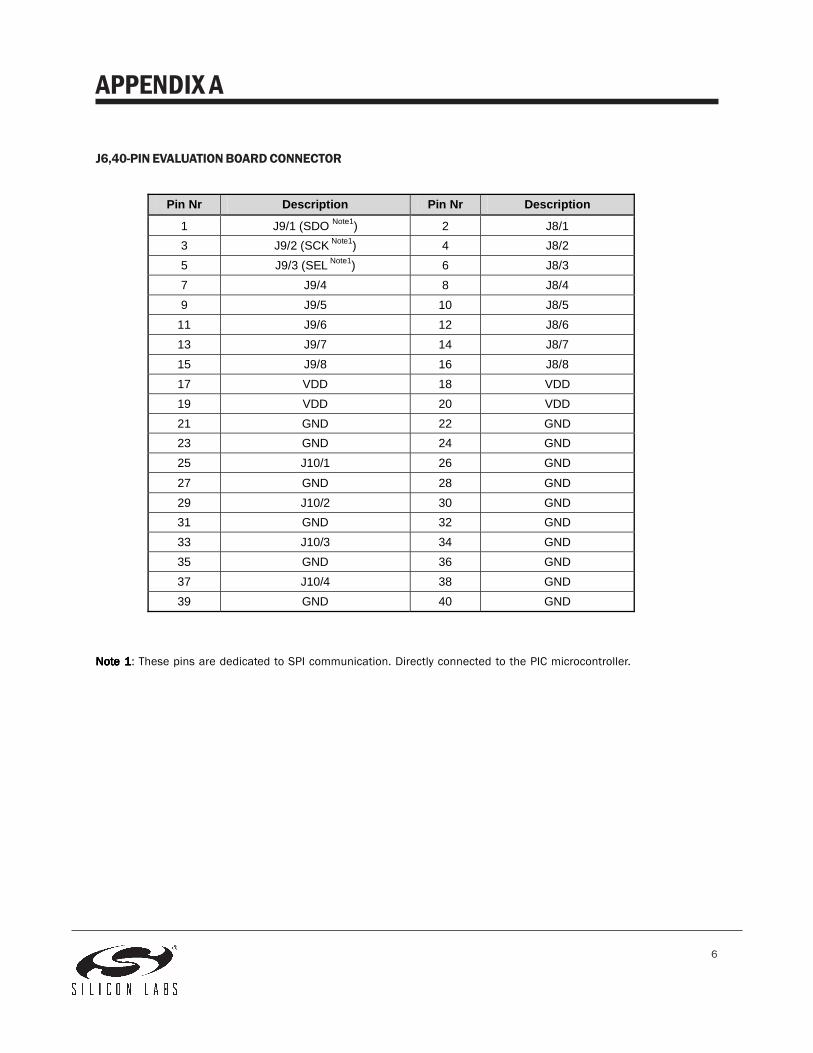
J6,40-PIN EVALUATION BOARD CONNECTOR
NoNoNoNoNottttte 1e 1e 1e 1e 1: These pins are dedicated to SPI communication. Directly connected to the PIC microcontroller.
APPENDIX A
Pin Nr Description Pin Nr Description
1 J9/1 (SDO Note1) 2 J8/1 3 J9/2 (SCK Note1) 4 J8/2 5 J9/3 (SEL Note1) 6 J8/3 7 J9/4 8 J8/4 9 J9/5 10 J8/5
11 J9/6 12 J8/6 13 J9/7 14 J8/7 15 J9/8 16 J8/8 17 VDD 18 VDD 19 VDD 20 VDD 21 GND 22 GND 23 GND 24 GND 25 J10/1 26 GND
27 GND 28 GND 29 J10/2 30 GND 31 GND 32 GND 33 J10/3 34 GND 35 GND 36 GND 37 J10/4 38 GND 39 GND 40 GND

7
APPENDIX A
EZRADIO TRANSMITTER EVALUATION BOARD PINOUT
For more details about the testboards, see the ISM Testboard User Guide: IA ISM-UGDB.
4220 connection (pin) 4220 connection (pin)
1 SDI (#1) 2 uC CLK (#8, filtered) 3 SCK (#2) 4 nIRQ (#14) 5 SEL (#3) 6 7 8 9 10 11 12 13 14 15 16 nIRQ (#14) 17 18 19 20 VDD 21 VSS (#10) 22 VSS 23 VSS 24 VSS 25 Ext clk (#9 optional, 10MHz) 26 VSS
27 VSS 28 VSS 29 FSK (#16) 30 VSS 31 VSS 32 VSS 33 uC CLK (#8) 34 VSS 35 VSS 36 VSS 37 VSS 38 VSS 39 VSS 40 VSS
8
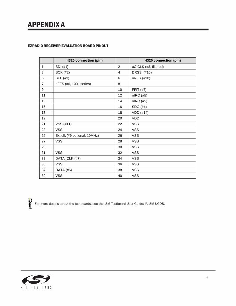
EZRADIO RECEIVER EVALUATION BOARD PINOUT
APPENDIX A
For more details about the testboards, see the ISM Testboard User Guide: IA ISM-UGDB.
4320 connection (pin) 4320 connection (pin)
1 SDI (#1) 2 uC CLK (#8, filtered) 3 SCK (#2) 4 DRSSI (#16) 5 SEL (#3) 6 nRES (#10) 7 nFFS (#6, 100k series) 8 9 10 FFIT (#7) 11 12 nIRQ (#5) 13 14 nIRQ (#5) 15 16 SDO (#4) 17 18 VDD (#14) 19 20 VDD 21 VSS (#11) 22 VSS 23 VSS 24 VSS 25 Ext clk (#9 optional, 10MHz) 26 VSS 27 VSS 28 VSS 29 30 VSS 31 VSS 32 VSS 33 DATA_CLK (#7) 34 VSS 35 VSS 36 VSS 37 DATA (#6) 38 VSS 39 VSS 40 VSS

9
ISM ProductsISM ProductsISM ProductsISM ProductsISM Products
IA4220 Transmitter ............11IA4320 Receiver ................23IA4420 Transceiver ............34
TABLE OF CONTENTS
Tutorials

10
This page is intentionally left blank

11
IA4220 TRANSMITTER
Tutorial

12
TUTORIAL: IA4220 TRANSMITTER
PACKET TRANSMISSION USING THE PIC WIRELESS DEVELOPMENT BOARD AND AN IA4220
Preparing the Hardware
The firmware needs the following hardware elements:
- PIC Wireless Development Board
- 915 MHz transmitter evaluation board (with any kind of on-board PCB antenna)
- PIC16LF876 microcontroller with PIC_Tx firmware loaded.
Important!Important!Important!Important!Important! The example program operates the IA4220 in the 915 MHz band. For proper operation plug a 915MHz transmitterevaluation board into the socket J6, such as the IA4220-DKDB2 (915 MHz BIFA antenna design).
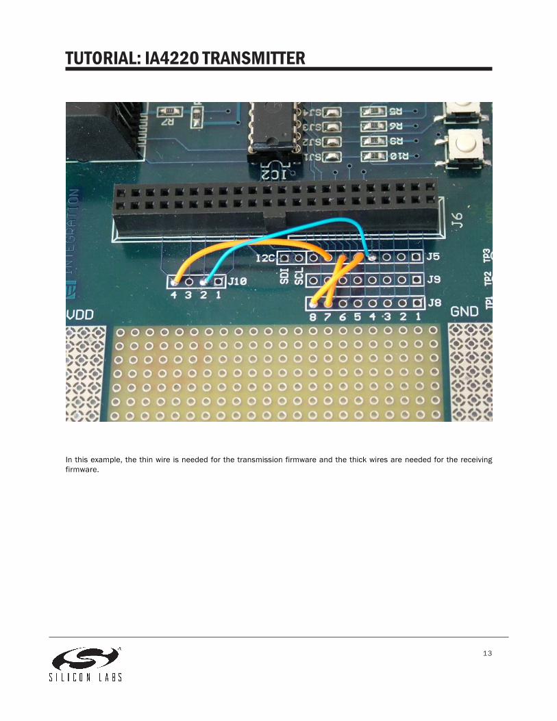
The example firmware demonstrates the operation of the IA4220 transmitter in microcontroller mode. The MOD pin of theIA4220 should be pulled to VDD. This is the default wiring on the transmitter evaluation boards.The microcontroller and the IA4220 should be connected with 4 wires:
NoteNoteNoteNoteNote: Please refer to Appendix A of the main chapter for connector pinouts.
The SPI wires are connected directly to the appropriate pin of the RF evaluation board connector, but the FSK line should becompleted by the following patch wire:
Name PIC IA4220
SPI SEL RB5 nSEL(#3) SPI SCK RB4 SCK(#2) SPI SDO RB3 SDI(#1)
FSK RB2 FSK(#16)
PIC IA 4220
J5/4 J10/2
13
TUTORIAL: IA4220 TRANSMITTER
In this example, the thin wire is needed for the transmission firmware and the thick wires are needed for the receivingfirmware.

14
Operation of the firmware
The example uses PB1, PB2, PB3 push buttons and D1, D2, D3 LEDs.
After power-on, the microcontroller initializes the transmitter without turning on the synthesizer and the power amplifier(PA).
Data packet transmissionData packet transmissionData packet transmissionData packet transmissionData packet transmission
Pressing PB1, the D1 LED flashes, the microcontroller turns on the synthesizer and the PA, builds the following packet, andtransmits it at 9600bps:
After the whole packet has been transmitted the microcontroller turns off the synthesizer and the PA.
CW testCW testCW testCW testCW test
Pressing and holding down PB2, the D2 LED flashes, the microcontroller turns on the synthesizer, and the PA and continuouslytransmitting 0s (transmitting fo-df frequency) until the button is released. Pressing and holding down PB3, the D3 LEDflashes, the microcontroller turns on the synthesizer and the PA and continuously transmitting 1s (transmitting fo+dffrequency) until the button is released.This continuous wave (CW) mode can be used to check the RF link before trying to transmit data packets. In CW test mode,the receiver should operate in normal mode (FIFO is disabled). In this mode, the pin#6 of the receiver operates as raw dataoutput and consistently follows the FSK input of the receiver. If the link is not perfect, the data output of the receiver isindefinite.
TUTORIAL: IA4220 TRANSMITTER
AA AA AA 2D D4 75 74 74
Databytes (received in the FIFO of the receive r)
42 6F 6E 31 0D
Preamble
Synchron pattern
‘B’ ‘u’ ‘t’ ‘t’ ‘o’ ‘n’ ‘1’ ‘CR’

15
SOURCE CODE
//////////////////////////////////////////////////////////////////////////////////// FW: Packet transmission using IA4220// HW: PIC Wireless Development board.// Note: J5/4 should be connected to J10/2// Version: 1v0//////////////////////////////////////////////////////////////////////////////////
#include <16F876.h>#device *=16#fuses hs,noprotect,nowdt,put,nolvp
#use delay(clock=10000000) // 10 MHz crystal is used#use rs232(baud=19200,xmit=PIN_C6,rcv=PIN_C7) // hw uart
#use fast_io(A)#use fast_io(B)#use fast_io(C)
Following are the PIC I/O definitions. All the I/Os except FSK are printed wires on the PCB. PIN_B2 should be manuallyconnected to the FSK pin (#16) of the transmitter. This can be done on the development board by connecting pin #2 of J10to pin #4 of J5.
#define LED1 PIN_C0#define LED2 PIN_C1#define LED3 PIN_C2#define LED4 PIN_C5#define BUT1 PIN_A2#define BUT2 PIN_A3#define BUT3 PIN_A4#define BUT4 PIN_A5
#define FSK PIN_B2#define SPI_SDO PIN_B3#define SPI_SCK PIN_B4#define SPI_SEL PIN_B5
Following are the global variable definitions. intintintintint means an 8-bit unsigned number, while longlonglonglonglong means a 16-bit one.
// Global variables:/ / — — — — — — — — — — -— — — — — — — — — — — — — — — — — — — —int i;int TxPacket[20]; // Transmit data puffer (with packet header)int TxPacketPtr; // Next byte to sendint TxPacketLen; // Tx packet size (with packet header)
TUTORIAL: IA4220 TRANSMITTER

16
int BitToSend;int nrofbits;int spidata;long Configuration_cmd;long Frequency_cmd;int Output_power_cmd;long Power_management_cmd;
The following is an SPI write subroutine which simply shifts out all the bits of the spidata global variable via the SPI_SDO pin.MSB is the first. After each shift a one clock pulse is generated.Note: the routine does not control the chip select signal of the SPI interface (SPI_SEL), this should be done before and aftercalling this routine.
// SPI interface write // send spidata via SPI/ / — — — — — — — — — — — — — — — — — — — — — — — — — — — — — — —void spi_write_sw(void) { int i; output_bit(SPI_SDO, 0); output_bit(SPI_SCK, 0); for (i=0;i<8;i=i+1) { BitToSend = shift_left(&spidata, 1, 0); // Shift out MSB first output_bit(SPI_SDO, BitToSend); output_bit(SPI_SCK, 1); // CLK pulse output_bit(SPI_SCK, 0); } output_bit(SPI_SDO, 0); }
The next subroutine is called once after power-up. Initializes the port directions, sets the SPI interface, FSK pin and theLEDs to default state.Also the transmitter commands are defined. Note: the power management command does not turn on the RF parts of thechip.At the end of the routine the commands are sent by the spi_write_sw() subroutine.
// initialization/ / — — — — — — — — — — — — — — — — — — — — — — — — — — — — — — —void MAIN_init(void) { set_tris_a(0b11111111); // set data I/O directions set_tris_b(0b11000011); set_tris_c(0b11011000);
output_low(SPI_SCK); // set SPI and FSK to default state output_high(SPI_SEL); output_low(FSK);
output_high(LED1); // switch off the LEDs at power-on output_high(LED2); output_high(LED3); output_high(LED4);
TUTORIAL: IA4220 TRANSMITTER

17
Important:Important:Important:Important:Important: the band selector command (Configuration Command) should be sent prior to the power management command.The reason is that after band selection, the synthesizer should be calibrated. Calibration can be done by turning (off and) onthe synthesizer with the power management command. In the current application, the synthesizer and the power amplifieris turned on before transmission starts, and turned off after the transmission has been finished.
//—— configuring the RF link ——————————————— Configuration_cmd = 0x9832; // Cload=10pF; df=90kHz Frequency_cmd = 0xA7D0; // Fo=915.000MHz Output_power_cmd = 0xB0; // FSK; Pmax Power_management_cmd = 0xC020; // Manual; Crystal osc. is on; synth. and the PA are off
//—— Sending Configuration command ———————————— output_low(SPI_SEL); spidata = (Configuration_cmd & 0xFF00) >> 8; spi_write_sw(); spidata = Configuration_cmd & 0x00FF; spi_write_sw(); output_high(SPI_SEL);
//—— Sending Frequency command —————————————— output_low(SPI_SEL); spidata = (Frequency_cmd & 0xFF00) >> 8; spi_write_sw(); spidata = Frequency_cmd & 0x00FF; spi_write_sw(); output_high(SPI_SEL);
//—— Sending Output power command ———————————— output_low(SPI_SEL); spidata = Output_power_cmd; spi_write_sw(); output_high(SPI_SEL);
//—— Sending Power management command —————————— output_low(SPI_SEL); spidata = (Power_management_cmd & 0xFF00) >> 8; spi_write_sw(); spidata = Power_management_cmd & 0x00FF; spi_write_sw(); output_high(SPI_SEL); }
Following is a non-important subroutine. This simply sends a welcome message via the RS232 port. It also prints thefirmware version information .
// print to the serial port/ / — — — — — — — — — — — — — — — — — — — — — — — — — — — — — — —void printabout(void) { printf(“\n\rWireless Development Board”);
TUTORIAL: IA4220 TRANSMITTER
NoteNoteNoteNoteNote: Configuration Commands etc., can easily becalculated in WDS

18
printf(“\n\rPIC platform, transmitter side\n\rV1.0 Integration, 2005\n\r”); }
The real program starts here. After power-on, the first two tasks are the initialization and sending the welcome message. Themain loop starts after that. While (1)While (1)While (1)While (1)While (1) means that it is a never ending loop.
//********************************************************************************************// M A I N P R O G R A M//********************************************************************************************
void main(void) // Program start point { MAIN_init(); // Main init rutin printabout(); // Welcome message to the serial port
//—— Foreground loop ——————————————————— while(1) // foreground loop, always running {
If button#1 is pressed, the LED1 will blink, after that the synthesizer and the power amplifier will be turn on. Next will be thepacket building, followed by the transmission via the FSK pin, and the synthesizer and the power amplifier will be turned offat the end.
// Actions if button1 pressed//============================================================= if(input(BUT1) == 0) { output_low(LED1); // blink LED1 delay_ms(100); output_high(LED1);
//—— Turn on sythesizer and the power amplifier ————— Power_management_cmd = 0xC038; // turn on the osc., synthesizer and the PA output_low(SPI_SEL); spidata = (Power_management_cmd & 0xFF00) >> 8; spi_write_sw(); spidata = Power_management_cmd & 0x00FF; spi_write_sw(); output_high(SPI_SEL);
//—— Tx packet building ————————————————— TxPacket[0] = 0xAA; // byte0: preamble TxPacket[1] = 0xAA; // byte1: preamble TxPacket[2] = 0xAA; // byte2: preamble TxPacket[3] = 0x2D; // byte3: sync byte#1 TxPacket[4] = 0xD4; // byte4: sync byte#2 TxPacket[5] = ‘B’; // first byte of the payload TxPacket[6] = ‘u’; TxPacket[7] = ‘t’; TxPacket[8] = ‘t’; TxPacket[9] = ‘o’;
TUTORIAL: IA4220 TRANSMITTER

19
TxPacket[10] = ‘n’; TxPacket[11] = ‘1’; TxPacket[12] = 13; // EOP: CR
TxPacketLen = 13; TxPacketPtr = 0; nrofbits = TxPacketLen * 8;
Note:Note:Note:Note:Note: the following algorithm sends all the databits with a single loop. This ensures transmission without having any gapbetween the bytes.Important!Important!Important!Important!Important! The loop is using a software delay to generate the correct datarate. The result is 9615bps which is close to thereceiver’s expected datarate (9579bps). Generally do not let the transmitter-receiver datarate error go higher than 1%.
//—— Packet transmission ————————————————— for(i=0;i<nrofbits;i=i+1) // sending all the bits via the FSK pin { TxPacketPtr = i / 8; // setting the pointer to the actual byte BitToSend = shift_left(&TxPacket[TxPacketPtr],1,0); // shifting out a bit if(BitToSend == 1) // testing the bit { output_bit(FSK, 1); // FSK = 1 delay_us(90); // set bittime to 104us } else { output_bit(FSK, 0); // FSK = 0 delay_us(91); // set bittime to 104us } } output_low(FSK); // After the transmission FSK = 0
Turning off the transmitter and waiting for releasing the button.
//—— Turn off sythesizer and the power amplifier ————— Power_management_cmd = 0xC020; // Crystal osc. is on; synth. and the PA are off output_low(SPI_SEL); spidata = (Power_management_cmd & 0xFF00) >> 8; spi_write_sw(); spidata = Power_management_cmd & 0x00FF; spi_write_sw(); output_high(SPI_SEL); while(input(BUT1) == 0) // wait for releasing Button1 {} delay_ms(10); // debouncing period }
If button#2 is pressed, the transmitter is turned on. The FSK pin of the transmitter will be pulled down, so the transmitteris continuously transmitting on the fo-df frequency. This is a simple and useful continuous wave (CW) link test.
TUTORIAL: IA4220 TRANSMITTER

20
For the CW test, the receiver should be configured to normal mode (the FIFO should be disabled).
// Actions if button2 pressed//============================================================= if(input(BUT2) == 0) {//—— Turn on sythesizer and the power amplifier ————— Power_management_cmd = 0xC038; // turn on the osc., synthesizer and the PA output_low(SPI_SEL); spidata = (Power_management_cmd & 0xFF00) >> 8; spi_write_sw(); spidata = Power_management_cmd & 0x00FF; spi_write_sw(); output_high(SPI_SEL);
output_low(LED2); // turn on LED2 output_low(FSK); // set FSK to logic low (Fout = Fo - df) while(input(BUT2) == 0) // wait for releasing Button2 {} output_high(LED2); // turn off LED2
//—— Turn off sythesizer and the power amplifier ————— Power_management_cmd = 0xC020; // Crystal osc. is on; synth. and the PA are off output_low(SPI_SEL); spidata = (Power_management_cmd & 0xFF00) >> 8; spi_write_sw(); spidata = Power_management_cmd & 0x00FF; spi_write_sw(); output_high(SPI_SEL); }
If button#3 is pressed, the transmitter is turned on. The FSK pin of the transmitter will be pulled up, so the transmitter iscontinuously transmitting on the fo+df frequency.
// Actions if button3 pressed//============================================================= if(input(BUT3) == 0) {//—— Turn on sythesizer and the power amplifier ————— Power_management_cmd = 0xC038; // turn on the osc., synthesizer and the PA output_low(SPI_SEL); spidata = (Power_management_cmd & 0xFF00) >> 8; spi_write_sw(); spidata = Power_management_cmd & 0x00FF; spi_write_sw(); output_high(SPI_SEL);
output_low(LED3); // turn on LED3 output_high(FSK); // set FSK to logic high (Fout = Fo + df) while(input(BUT3) == 0) // wait for releasing Button3 {}
TUTORIAL: IA4220 TRANSMITTER

21
output_high(LED3); // turn off LED3
//-— Turn off sythesizer and the power amplifier ————— Power_management_cmd = 0xC020; // Crystal osc. is on; synth. and the PA are off output_low(SPI_SEL); spidata = (Power_management_cmd & 0xFF00) >> 8; spi_write_sw(); spidata = Power_management_cmd & 0x00FF; spi_write_sw(); output_high(SPI_SEL); } } }
TUTORIAL: IA4220 TRANSMITTER

22
APPENDIX
PIC_TX FIRMWARE REVISION HISTORY
V 1.0:V 1.0:V 1.0:V 1.0:V 1.0: Initial release
0505

23
IA4320 RECEIVER
Tutorial
24
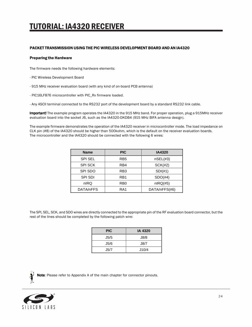
TUTORIAL: IA4320 RECEIVER
PACKET TRANSMISSION USING THE PIC WIRELESS DEVELOPMENT BOARD AND AN IA4320
Preparing the Hardware
The firmware needs the following hardware elements:
- PIC Wireless Development Board
- 915 MHz receiver evaluation board (with any kind of on-board PCB antenna)
- PIC16LF876 microcontroller with PIC_Rx firmware loaded.
- Any ASCII terminal connected to the RS232 port of the development board by a standard RS232 link cable.
Important!Important!Important!Important!Important! The example program operates the IA4320 in the 915 MHz band. For proper operation, plug a 915MHz receiverevaluation board into the socket J6, such as the IA4320-DKDB4 (915 MHz BIFA antenna design).
The example firmware demonstrates the operation of the IA4320 receiver in microcontroller mode. The load impedance onCLK pin (#8) of the IA4320 should be higher than 500kohm, which is the default on the receiver evaluation boards.The microcontroller and the IA4320 should be connected with the following 6 wires:
NoteNoteNoteNoteNote: Please refer to Appendix A of the main chapter for connector pinouts.
The SPI, SEL, SCK, and SDO wires are directly connected to the appropriate pin of the RF evaluation board connector, but therest of the lines should be completed by the following patch wire:
Name PIC IA4320
SPI SEL RB5 nSEL(#3) SPI SCK RB4 SCK(#2) SPI SDO RB3 SDI(#1) SPI SDI RB1 SDO(#4)
nIRQ RB0 nIRQ(#5) DATA/nFFS RA1 DATA/nFFS(#6)
PIC IA 4320
J5/5 J8/8 J5/6 J8/7 J5/7 J10/4

25
TUTORIAL: IA4320 RECEIVER
Operation of the firmware
The example uses PB1 push button and D1, D2, D4 LEDs.
After power-on, the microcontroller initializes the transmitter in FIFO mode with the right rf and datarate settings. Thereceiver is waiting for an incoming packet. The packet structure should be the following:
Data packet receivingData packet receivingData packet receivingData packet receivingData packet receiving
If the receiver receives a data packet, the D4 LED will flash, and the received data packet will be sent to the RS232 port ofthe board both in ASCII and hexadecimal format. The communication settings are:
Three bytes of AA (hexadecimal) is needed for the clock recovery circuit to generate the right dataclock. The preamble isfollowed by the 16-bit synchron pattern 2D D4 (hexadecimal). The first byte received after the synchron pattern will be thefirst byte in the FIFO.
CW testCW testCW testCW testCW test
Pressing and holding down PB1, the microcontroller switches the receiver to normal mode. D1 and D2 LEDs will indicate thestate of the raw data output (pin#6) of the receiver.
The continuous wave (CW) test is used to check the RF link before trying to transmit data packets. The transmitter shouldcontinuously transmit 0 or 1 and if the link is OK the D1 and D2 LEDs will indicate on the receiver side accordingly. If thelink is not perfect, the data output of the receiver is indefinite, so both D1 and D2 will flash at 50% duty.
AA AA AA 2D D4
Databytes (received in the FIFO of the receiver)
Preamble
Synchron pattern
D0 D1 D2 . . . DN
Parameter Value
Baud rate: 19200 Data bits: 8 Stop bits: 1 Parity: none Flow control: no

26
TUTORIAL: IA4320 RECEIVER
SOURCE CODE
//////////////////////////////////////////////////////////////////////////////////// FW: Packet receiving using IA4320// HW: PIC Wireless Development board.// Note: J5/5 should be connected to J8/8// Note: J5/6 should be connected to J8/7// Note: J5/7 should be connected to J10/4// Version: 1v0//////////////////////////////////////////////////////////////////////////////////
#include <16F876.h>#device *=16#fuses hs,noprotect,nowdt,put,nolvp
#use delay(clock=10000000) // 10 MHz crystal is used#use rs232(baud=19200,xmit=PIN_C6,rcv=PIN_C7) // hw uart
#use fast_io(A)#use fast_io(B)#use fast_io(C)
Following are the PIC I/O definitions. The SPI_SDI, RX_IRQ and the DATA_NFFS port connections should be manually createdby patch wires as it is described in the section Preparing the hardware.
#define LED1 PIN_C0#define LED2 PIN_C1#define LED3 PIN_C2#define LED4 PIN_C5#define BUT1 PIN_A2#define BUT2 PIN_A3#define BUT3 PIN_A4#define BUT4 PIN_A5
#define SPI_SDO PIN_B3#define SPI_SCK PIN_B4#define SPI_SEL PIN_B5#define SPI_SDI PIN_B1 // receiver ship SDO#define RX_IRQ PIN_B0 // receiver chip nIRQ#define DATA_NFFS PIN_A1 // in FIFO mode: nFFS; in normal mode: DATA out
The maximum length of the received data packet is defined here (in data bytes).
#define MAX_LENGTH 16
#use fast_io(A)#use fast_io(B)#use fast_io(C)
Following are the global variable definitions. intintintintint means an 8-bit unsigned number, while longlonglonglonglong means a 16-bit one.

27
TUTORIAL: IA4320 RECEIVER
// Global variables:/ / — — — — — — — — — — — — — — — — — — — — — — — — — — — — — — —int i;
The following 4 variables store the value of the interrupt flags. The variables are updated during the receiver status read.
int ffit; // IT flagsint ffof;int wkup;int lbd;
int RxPacket[MAX_LENGTH]; // Receive data pufferint RxPacketPtr; // Next byte to to receiveint RxPacketLen; // Expected packet size (excluding packet header)int BitToSend;int spidata; // 8-bit global variable for spi read/write instructionslong spicmd; // 16-bit global variable for sending spi commands to the rf chiplong Configuration_cmd;long Frequency_cmd;long Receiver_cmd;long FIFO_cmd;long Data_filter_cmd;long Data_rate_cmd;long AFC_cmd;
The following three subroutines are the SPI interface routines.The first routine reads 8 bit from the SPI interface of the receiver and saves it to the spidata global variable.The next sends the spidata variable (8 bits) to the receiver via the SPI interfaceThe third routine sends the spicmd variable (16 bits) to the receiver via the SPI interface. MSB is always first.Note: the routines do not control the chip and FIFO select signals of the SPI interface. These should be done before and aftercalling this routine.
// SPI interface read: reads 8 bits from the SPI and saves it to spidata/ / — — — — — — — — — — — — — — — — — — — — — — — — — — — — — — —void spi_read_sw(void) { int i; output_low(SPI_SDO); output_low(SPI_SCK); for (i=0;i<8;i=i+1) { shift_left(&spidata, 1, input(SPI_SDI)); output_high(SPI_SCK); output_low(SPI_SCK); } }
// SPI interface write: sends the spidata (8 bits) via SPI/ / — — — — — — — — — — — — — — — — — — — — — — — — — — — — — — —void spi_write_sw(void) {

28
TUTORIAL: IA4320 RECEIVER
int i; output_low(SPI_SDO); output_low(SPI_SCK); for (i=0;i<8;i=i+1) { BitToSend = shift_left(&spidata, 1, 0); // Shift out MSB first output_bit(SPI_SDO, BitToSend); output_high(SPI_SCK); // CLK pulse output_low(SPI_SCK); } output_low(SPI_SDO); }
// SPI interface write: sends the spicmd (16 bits) via spi/ / — — — — — — — — — — — — — — — — — — — — — — — — — — — — — — —void send_cmd(void) { output_low(SPI_SEL); spidata = (spicmd & 0xFF00) >> 8; spi_write_sw(); spidata = spicmd & 0x00FF; spi_write_sw(); output_high(SPI_SEL); }
The next subroutine is called once after power-up. Initializes the port directions, sets the SPI interface, nFFS pin and theLEDs to default state.The transmitter commands are also defined. Note: the power management command does not turn on the RF parts of thechip.At the end of the routine the commands are sent by the spi_write_sw() subroutine.
// initialization/ / — — — — — — — — — — — — — — — — — — — — — — — — — — — — — — —void MAIN_init(void) { set_tris_a(0b11111101); // set data I/O directions set_tris_b(0b11000011); set_tris_c(0b11011000);
output_low(SPI_SCK); // set SPI to default state output_high(SPI_SEL); output_high(DATA_NFFS); // nFFS inactive
output_high(LED1); // switch off the LEDs at power-on output_high(LED2); output_high(LED3); output_high(LED4); RxPacketPtr = 0;

29
TUTORIAL: IA4320 RECEIVER
Following is the configuration of the RF link.Important:Important:Important:Important:Important: The band selector command (Configuration Command) should be sent prior to the receiver command. Thereason is that after band selection, the synthesizer should be calibrated. Calibration can be done by turning (off and) on thereceiver chain by the receiver command. In the current application the receiver chain is continuously turned on.The FIFO command is also sent twice. First with synchron latch reset and then with synchron latch enable settings. This waythe FIFO is reset and waiting for receiving the synchron pattern. Once the synchron pattern has been received the FIFO fillwill start, and all the databits received will fill the FIFO until the next synchron latch reset (or FIFO disable).
// configuring the RF link:/ / — — — — — — — — — — — — — — — — — Configuration_cmd = 0x9938; // Cload=10pF; 915MHz, bw filter=200kHz; Crystal osc. is on Frequency_cmd = 0xA7D0; // Fo=915.000MHz Receiver_cmd = 0xC080; // VDI=CRL;LNA gain=max.;Receiver chain is off FIFO_cmd = 0xCE85; // Enable FIFO; IT level=8; Synch. pattern; reset synchron latch Data_filter_cmd = 0xC4AC; // Digital LPF;Clk recovery is in auto mode;DQD parameter=4 Data_rate_cmd = 0xC823; // Data rate=9579bps AFC_cmd = 0xC6FE; // Disable AFC
spicmd = Configuration_cmd; send_cmd(); spicmd = Frequency_cmd; send_cmd(); spicmd = Receiver_cmd; send_cmd(); spicmd = Receiver_cmd | 0x0001;// turn on the receiver chain (calibrate the synthesizer) send_cmd(); spicmd = FIFO_cmd; send_cmd(); spicmd = FIFO_cmd | 0x0002; // enable synchron latch send_cmd(); spicmd = Data_filter_cmd; send_cmd(); spicmd = Data_rate_cmd; send_cmd(); spicmd = AFC_cmd; send_cmd(); }
Following is a non-important subroutine. This simply sends a welcome message via the RS232 port. It also prints thefirmware version information.
// print to the serial port/ / — — — — — — — — — — — — — — — — — — — — — — — — — — — — — — —void printabout(void) { printf(“\n\rWireless Development Board”); printf(“\n\rPIC platform, receiver side\n\rV1.0 Integration, 2005\n\r”); }
The real program starts here. After power-on, the first two tasks are the initialization and sending the welcome message. Themain loop starts after that. While(1)While(1)While(1)While(1)While(1) means that it is a never ending loop.

30
TUTORIAL: IA4320 RECEIVER
//===============================================================================================void main(void) // program bel¨¦p¨¦si pont { MAIN_init(); // Main init rutin printabout(); // Welcome message while(1) // foreground loop {
The foreground loop is continuously polling the nIRQ pin of the receiver. If the nIRQ is active (low), the microcontroller startsa status read. The first 4 bits of the status word are the interrupt flags. The very first is the FIFO IT.
while(input(RX_IRQ) == 0) // polling the nIRQ pin of the chip { output_low(LED4); // LED4 incicates packet receiving
output_low(SPI_SCK); output_low(SPI_SDO); output_high(DATA_NFFS); // nFFS inactive
output_low(SPI_SEL); ffit = input(SPI_SDI); output_high(SPI_SCK); output_low(SPI_SCK); ffof = input(SPI_SDI); output_high(SPI_SCK); output_low(SPI_SCK); wkup = input(SPI_SDI); output_high(SPI_SCK); output_low(SPI_SCK); lbd = input(SPI_SDI); output_high(SPI_SCK); output_low(SPI_SCK); output_high(SPI_SEL);
After reading the IT flags, the status read was aborted by switching SPI_SEL to high.The next step is the testing of the FIFO IT flag if is high or not. If it is high, the FIFO will be selected and 8 received databit willbe read out.
if(ffit) // Read out the FIFO in case of FFIT { output_low(SPI_SEL); output_low(DATA_NFFS); // FIFO selected spi_read_sw(); output_high(SPI_SEL); output_high(DATA_NFFS); // FIFO deselected RxPacket[RxPacketPtr] = spidata; RxPacketPtr = RxPacketPtr + 1; }
Now the program is testing the end of packet condition. Here we are using a very simple condition: If the number of the lastreceived databyte is a carriage return character or the received databits is higher than MAX_LENGTH, the synchron latch willbe reset, and the FIFO will wait for the next synchron pattern.

31
TUTORIAL: IA4320 RECEIVER
if ((spidata == ‘\r’) || (RxPacketPtr >= MAX_LENGTH)) // End of packet condition { spicmd = FIFO_cmd; // FIFO synchron latch reset send_cmd(); spicmd = FIFO_cmd | 0x0002; // FIFO synchron latch enable send_cmd(); RxPacketLen = RxPacketPtr; RxPacketPtr = 0;
The received packet is printed to the RS232 port both in ASCII and hexadecimal format:
printf(“\r\n”); for(i=0;i<RxPacketLen;i=i+1) { putc(RxPacket[i]); } printf(“\r\n”); for(i=0;i<RxPacketLen;i=i+1) { printf(“%X “, RxPacket[i]); } printf(“\r\n”); output_high(LED4); } }
If button#1 is pressed, the microcontroller switches the receiver to normal mode by the FIFO command. In this mode theFIFO is disabled, the DATA/nFFS pin (#6) of the receiver operates as raw data output. The DATA_NFFS pin of the PIC shouldbe configured to input.
// Button1 service routine//============================================================= if(input(BUT1) == 0) { delay_ms(10); // debounce period spicmd = FIFO_cmd & 0xFFFC; // disable FIFO, synchron latch send_cmd(); set_tris_a(0b11111111); // configure DATA_NFFS to input
While button#1 is held down, the microcontroller is polling the DATA_NFFS input. If the input is low the LED D1 will be turnedon, LED D2 will be turned off, and if the input is high the LED D1 will be turned off, LED D2 will be turned on.
while(input(BUT1) == 0) // Do until Button1 is pressed { if(input(DATA_NFFS) == 0) { output_low(LED1); output_high(LED2); } else {

32
TUTORIAL: IA4320 RECEIVER
output_low(LED2); output_high(LED1); } }
After the button is released, the microcontroller turns off the LEDs, and switches the receiver to FIFO mode again.
output_high(LED1); output_high(LED2); spicmd = FIFO_cmd | 0x0002; // enable FIFO, synchron latch send_cmd(); set_tris_a(0b11111101); // configure DATA_NFFS to output } } }

33
APPENDIX
PIC_RX FIRMWARE REVISION HISTORY
V 1.0:V 1.0:V 1.0:V 1.0:V 1.0: Initial release
0505

34
This page is intentionally left blank

35
IA4420 TRANSCEIVER
Tutorial

36
TUTORIAL: IA4420 TRANSCEIVER
//////////////////////////////////////////////////////////////////////////////////// FW: Packet transmission/receiving using IA4420// HW: PIC Wireless Development board.// Note: J5/4 should be connected to J10/2// Note: J5/5 should be connected to J8/8// Note: J5/6 should be connected to J8/7// Note: J5/7 should be connected to J10/4// Version: 1v0//////////////////////////////////////////////////////////////////////////////////
#include <16F876.h>#device *=16#fuses hs,noprotect,nowdt,put,nolvp
#use delay(clock=10000000) // 10 MHz crystal is used#use rs232(baud=19200,xmit=PIN_C6,rcv=PIN_C7) // hw usart
#use fast_io(A)#use fast_io(B)#use fast_io(C)
#define LED1 PIN_C0#define LED2 PIN_C1#define LED3 PIN_C2#define LED4 PIN_C5#define BUT1 PIN_A2#define BUT2 PIN_A3#define BUT3 PIN_A4#define BUT4 PIN_A5
#define SPI_SDI PIN_B1#define SPI_SDO PIN_B3#define SPI_SCK PIN_B4#define SPI_SEL PIN_B5#define RX_IRQ PIN_B0 // receiver chip irq#define DATA_NFFS PIN_A1 // receiving: in FIFO mode: NFFS; in normal mode: DATA out#define FSK PIN_A1 // transmission: FSK
#define MAX_LENGTH 40
SOURCE CODE

37
TUTORIAL: IA4420 TRANSCEIVER// Global variables://--------------------------------------------------------------int i;int ffit_rgit; // IT bit0int por;int ffof_rgur;int wkup;int ext;int lbd; // IT bit5int TxPacket[MAX_LENGTH + 7]; // Transmit data puffer (with packetheader + dummy bytes)int TxPacketPtr; // Next byte to sendint TxPacketLen; // Tx packet sizeint RxPacket[MAX_LENGTH]; // Receive data puffer (payload only)int RxPacketPtr; // Next byte to sendint RxPacketLen; // Rx packet size
int spidata;
long spicmd; // 16-bit global variable for sending spi commands to the rf chiplong Configuration_cmd;long Frequency_cmd;long Power_management_cmd;long Receiver_control_cmd;long Transmitter_control_cmd;long Txreg_write_cmd;long FIFO_cmd;long Data_filter_cmd;long Data_rate_cmd;long AFC_cmd;
// SPI interface read // read spidata from SPI//--------------------------------------------------------------void spi_read_sw(void) { int i; output_low(SPI_SDO); output_low(SPI_SCK); for (i=0;i<8;i=i+1) { shift_left(&spidata, 1, input(SPI_SDI)); output_high(SPI_SCK); output_low(SPI_SCK); } }

38
TUTORIAL: IA4420 TRANSCEIVER
// SPI interface write // send spidata via SPI//--------------------------------------------------------------void spi_write_sw(void) { int i; int BitToSend; output_low(SPI_SDO); output_low(SPI_SCK); for (i=0;i<8;i=i+1) { BitToSend = shift_left(&spidata, 1, 0); // Shift out MSB first output_bit(SPI_SDO, BitToSend); output_high(SPI_SCK); // CLK pulse output_low(SPI_SCK); } output_low(SPI_SDO); }
// Send SPI command to the rf chip // send 16-bit SPI command//--------------------------------------------------------------void send_cmd(void) { output_low(SPI_SEL); spidata = (spicmd & 0xFF00) >> 8; spi_write_sw(); spidata = spicmd & 0x00FF; spi_write_sw(); output_high(SPI_SEL); }
// initialization//--------------------------------------------------------------void MAIN_init(void) { set_tris_a(0b11111101); // set data I/O directions set_tris_b(0b11000111); set_tris_c(0b11011000);
output_low(SPI_SCK); // set SPI to default state output_high(SPI_SEL); output_high(DATA_NFFS); // nFFS inactive
output_high(LED1); // switch off the LED's at power-on output_high(LED2); output_high(LED3); output_high(LED4);

39
TUTORIAL: IA4420 TRANSCEIVER
RxPacketPtr = 0;
//---- Init the TxPacket with preamble and sync. pattern ------ TxPacket[0] = 0xAA; // byte0: preamble TxPacket[1] = 0xAA; // byte1: preamble TxPacket[2] = 0xAA; // byte2: preamble TxPacket[3] = 0x2D; // byte3: sync byte#1 TxPacket[4] = 0xD4;
//---- configuring the RF link -------------------------------- Configuration_cmd = 0x8073; // Cload=10pF; TX register disabled, FIFO enabled Frequency_cmd = 0xA7D0; // Fo=915.000MHz (default) Power_management_cmd = 0x8200; // Crystal osc., synthesizer, transmitter and receiver are off Receiver_control_cmd = 0x9481; // BW=200kHz, DRSSI=-97dBm, pin8=VDI, fast VDI Transmitter_control_cmd = 0x9850; // df=90kHz, Pmax, normal modulation polarity Txreg_write_cmd = 0xB800; FIFO_cmd = 0xCA81; // Sync. latch cleared, limit=8bits, disable sensitive reset Data_filter_cmd = 0xC22C; // Digital LPF (default) Data_rate_cmd = 0xC623; // 9579Baud (default) AFC_cmd = 0xC4F7; // Auto AFC (default) spicmd = FIFO_cmd; send_cmd(); spicmd = FIFO_cmd | 0x0002; // enable synchron latch send_cmd(); spicmd = Configuration_cmd; send_cmd(); spicmd = Frequency_cmd; send_cmd(); spicmd = Power_management_cmd; send_cmd(); spicmd = Receiver_control_cmd; send_cmd(); spicmd = Transmitter_control_cmd; send_cmd(); // antenna tuning on startup spicmd = Power_management_cmd | 0x0020; // turn on the transmitter send_cmd(); delay_ms(5); // ant.tuning time (~100us) + Xosc starup time (5ms) // end of antenna tuning spicmd = Power_management_cmd | 0x0080; // turn off transmitter, turn on receiver send_cmd(); }
// print to the serial port//--------------------------------------------------------------void printabout(void) { printf("\n\rWireless Development Board"); printf("\n\rPIC platform, transceiver side\n\rV1.0 Integration, 2005\n\r"); }

40
TUTORIAL: IA4420 TRANSCEIVER
//*************************************************************************************************// M A I N P R O G R A M//*************************************************************************************************
void main(void) // Program start point { MAIN_init(); // Main init rutin printabout(); // Welcome message to the serial port
//---- Foreground loop -------------------------------------- while(1) // foreground loop, always running {
// Actions if button1 pressed//============================================================= if(input(BUT1) == 0) { output_low(LED1); // blink LED1 delay_ms(100); output_high(LED1);
//---- Tx packet building ----------------------------------- TxPacket[5] = 'B'; // first byte of the payload TxPacket[6] = 'u'; TxPacket[7] = 't'; TxPacket[8] = 't'; TxPacket[9] = 'o'; TxPacket[10] = 'n'; TxPacket[11] = '1'; TxPacket[12] = 13; // EOP: CR TxPacket[13] = 13; // dummy TxPacket[14] = 13; // dummy
TxPacketLen = 15; // last two byte won't be transmitted
//---- Turn off receiver, enable the TX register ------------ spicmd = Power_management_cmd; // turn off the transmitter and thereceiver send_cmd(); spicmd = Configuration_cmd | 0x0080; // Enable the TX register send_cmd();
//---- Packet transmission ----------------------------------
// Load the first 2 bytes: spicmd = Txreg_write_cmd | TxPacket[0]; send_cmd(); spicmd = Txreg_write_cmd | TxPacket[1]; send_cmd(); // Enable transmitter: spicmd = Power_management_cmd | 0x0020; // turn on the transmitter send_cmd();
41
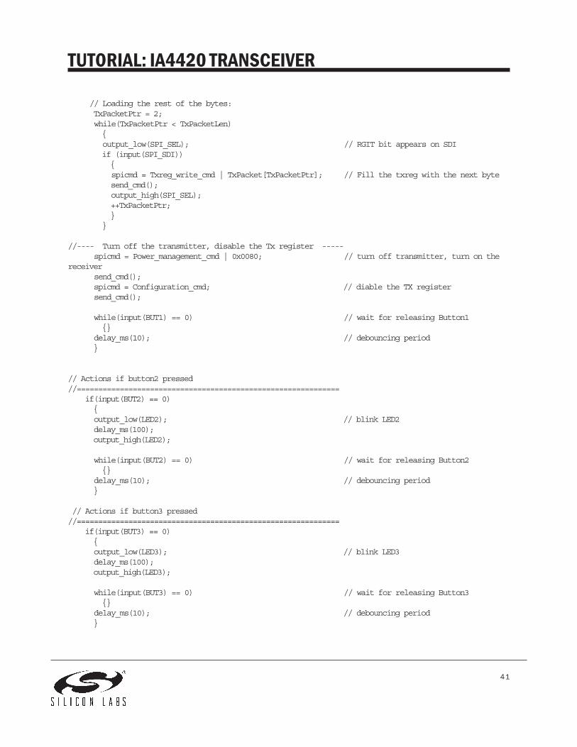
TUTORIAL: IA4420 TRANSCEIVER
// Loading the rest of the bytes: TxPacketPtr = 2; while(TxPacketPtr < TxPacketLen) { output_low(SPI_SEL); // RGIT bit appears on SDI if (input(SPI_SDI)) { spicmd = Txreg_write_cmd | TxPacket[TxPacketPtr]; // Fill the txreg with the next byte send_cmd(); output_high(SPI_SEL); ++TxPacketPtr; } }
//---- Turn off the transmitter, disable the Tx register ----- spicmd = Power_management_cmd | 0x0080; // turn off transmitter, turn on thereceiver send_cmd(); spicmd = Configuration_cmd; // diable the TX register send_cmd();
while(input(BUT1) == 0) // wait for releasing Button1 {} delay_ms(10); // debouncing period }
// Actions if button2 pressed//============================================================= if(input(BUT2) == 0) { output_low(LED2); // blink LED2 delay_ms(100); output_high(LED2);
while(input(BUT2) == 0) // wait for releasing Button2 {} delay_ms(10); // debouncing period }
// Actions if button3 pressed//============================================================= if(input(BUT3) == 0) { output_low(LED3); // blink LED3 delay_ms(100); output_high(LED3);
while(input(BUT3) == 0) // wait for releasing Button3 {} delay_ms(10); // debouncing period }

42
TUTORIAL: IA4420 TRANSCEIVER
// Actions if no button pressed//=============================================================
while(input(RX_IRQ) == 0) // polling the nIRQ pin of the chip { output_low(LED4); // LED4 incicates packet receiving output_low(SPI_SEL);
if(input(SPI_SDI)) // Read out the FIFO in case of FFIT { output_high(SPI_SEL); output_low(DATA_NFFS); // FIFO selected spi_read_sw(); output_high(DATA_NFFS); // FIFO deselected RxPacket[RxPacketPtr] = spidata; RxPacketPtr = RxPacketPtr + 1;
if ((spidata == '\r') || (RxPacketPtr >= MAX_LENGTH)) // End of packet condition { spicmd = FIFO_cmd; // FIFO synchron latch reset send_cmd(); spicmd = FIFO_cmd | 0x0002; // FIFO synchron latch enable send_cmd(); RxPacketLen = RxPacketPtr; RxPacketPtr = 0; printf("\r\n"); for(i=0;i<RxPacketLen;i=i+1) { putc(RxPacket[i]); } printf("\r\n"); for(i=0;i<RxPacketLen;i=i+1) { printf("%X ", RxPacket[i]); } printf("\r\n"); } } else // Read out the rest IT bits in caseof no FFIT {

43
TUTORIAL: IA4420 TRANSCEIVER
output_high(SPI_SCK); output_low(SPI_SCK); por = input(SPI_SDI); output_high(SPI_SCK); output_low(SPI_SCK); ffof_rgur = input(SPI_SDI); output_high(SPI_SCK); output_low(SPI_SCK); wkup = input(SPI_SDI); output_high(SPI_SCK); output_low(SPI_SCK); ext = input(SPI_SDI); output_high(SPI_SCK); output_low(SPI_SCK); lbd = input(SPI_SDI); output_high(SPI_SCK); output_low(SPI_SCK); // 6th clock pulse to reset the ITlatches output_high(SPI_SEL); }
output_high(LED4); } } }

44
APPENDIX
PIC_TRX FIRMWARE REVISION HISTORY
V 1.0:V 1.0:V 1.0:V 1.0:V 1.0: Initial release
1005

45
This page is intentionally left blank

46
Silicon Labs, Inc.400 West Cesar ChavezAustin, Texas 78701Tel: 512.416.8500Fax: 512.416.9669Toll Free: 877.444.3032www.silabs.com/[email protected] ©2008 Silicon Laboratories, Inc. All rights reserved. Silicon Laboratories is a trademark of Silicon Laboratories, Inc. All
other trademarks belong to their respective owners.
The specifications and descriptions in this document are based on information availableat the time of publication and are subject to change without notice. Silicon Laboratoriesassumes no responsibility for errors or omissions, and disclaims responsibility forany consequences resulting from the use of information included herein. Additionally,Silicon Laboratories assumes no responsibility for the functioning of undescribedfeatures or parameters. Silicon Laboratories reserves the right to make changes tothe product and its documentation at any time. Silicon Laboratories makes norepresentations, warranties, or guarantees regarding the suitability of its productsfor any particular purpose and does not assume any liability arising out of the applicationor use of any product or circuit, and specifically disclaims any and all liability forconsequential or incidental damages arising out of use or failure of the product.Nothing in this document shall operate as an express or implied license or indemnityunder the intellectual property rights of Silicon Laboratories or third parties. Theproducts described in this document are not intended for use in implantation or otherdirect life support applications where malfunction may result in the direct physicalharm or injury to persons. NO WARRANTIES OF ANY KIND, INCLUDING BUT NOTLIMITED TO, THE IMPLIED WARRANTIES OF MERCHANTABILITY OR FITNESS FOR APARTICULAR PURPOSE, ARE OFFERED IN THIS DOCUMENT.


