IBIS FORUM I/O BUFFER MODELING COOKBOOK Revision 2.0X (under development) Prepared By: The IBIS Open Forum Senior Editor: Stephen Peters Intel Corp. Sept 24, 1997 * Trademarks are the properties of their respective owners.
Transcript
IBIS FORUM I/O BUFFER MODELING COOKBOOK
Revision 2.0X (under development)
Prepared By:
The IBIS Open Forum
Senior Editor:
Stephen Peters Intel Corp.
Sept 24, 1997
* Trademarks are the properties of their respective owners.
1.1 Quick Overview of an IBIS File ............................................................................................1 1.2 Steps to creating an IBIS Model ............................................................................................2
Model Version and Complexity......................................................................................4 Specification Model vs. Part Model ..............................................................................4 Fast and Slow Corner Model Limits...............................................................................5 Inclusion of SSO Effects ................................................................................................5
2.2 Information Checklist ............................................................................................................5 2.3 Tips For Component Buffer Grouping ..................................................................................6
3.0 Extracting the Data .............................................................................................................................7 3.1 Using Spice to IBIS (s2ibis) ..................................................................................................7 3.2 Extracting I/V and Switching Data via Simulations..............................................................7 3.2.1 Extracting the I/V Data.......................................................................................................7
Simulation Setup.............................................................................................................7 3-state Buffers.................................................................................................................8 Output Only Buffers .......................................................................................................9 Open Drain Buffers.........................................................................................................9 Input Buffers ...................................................................................................................9 Sweep Ranges .................................................................................................................9 Making Pullup and Power Clamp Sweeps Vcc Relative................................................10 Diode Models..................................................................................................................10 Diode Transient Time Data ............................................................................................10
3.2.2 Extracting the Ramp Rate or V/T Waveform Data ............................................................11 Extracting Data for the [Ramp] Keyword ......................................................................11 Extracting Data for the Rising and Falling Waveform Keywords .................................12 Minimum Time Step.......................................................................................................13 Multi State Drivers .........................................................................................................13
3.3 Obtaining I/V and Switching Information via Lab Measurment ...........................................13 4.0 Putting the Data Into an IBIS File.......................................................................................................15
4.1 IBIS File Header Information ................................................................................................15 4.2 Component and Pin Information............................................................................................16 4.3 The [Model] Keyword ...........................................................................................................17
Parameter section............................................................................................................17 Temperature and Voltage Keywords ..............................................................................18 I/V data section ...............................................................................................................19 Pulldown .........................................................................................................................19 Ground Clamp.................................................................................................................20 Pullup..............................................................................................................................20 Power Clamp...................................................................................................................21 Extrapolation Errors .......................................................................................................21 [Ramp] and Waveform Tables........................................................................................21
5.0 Validating the Model ..........................................................................................................................23 6.0 Correlating the Data............................................................................................................................24 7.0 Resources ............................................................................................................................................25 Example 1 – Basic (Version 1.1) model ...................................................................................................26
Example 2 – Version 2.1 model of a Multi-supply PCI component.........................................................26 Example 3 – An Open Drain, Controlled Rise time (GTL) Model ..........................................................26 Example 4 – A device with differential pins ............................................................................................26 Example 5 – ECL devices.........................................................................................................................26
IBIS Forum I/O Buffer Modeling Cookbook Page 1
1.0 Introduction This cookbook describes the steps required to produce IBIS models for digital integrated circuits (ICs). IBIS (officially, EIA standard 656) stands for I/O Buffer Information Specification. IBIS models provide a standardized way of representing the electrical characteristics of an digital IC’s pins (input, output, or I/O buffers) behaviorally, i.e., without revealing the underlying circuit’s structure or process information.
The purpose of this document is to explain how to gather the information required to produce a IBIS model, as well as some of the common pitfalls to avoid when creating the IBIS file itself. Note that the basic behavioral information in an IBIS model can be obtained either by direct measurement of the device itself or transistor level simulation of the device’s circuits. This cookbook describes both methods. The cookbook is targeted towards generating models of CMOS, GTL, and bipolar parts, and applies to models generated for IBIS versions V1.1 and V2.1. For the most recent version of the specification, the latest version of the IBIS Overview, and other IBIS documents visit the IBIS web page. For access information, see the Resources section later in this cookbook.
The intended audience of this cookbook are those responsible for performing the measurements or simulations that gather I/O buffer data, as well as those responsible for actual IBIS model creation. Persons involved in SI or system level PC board simulations may also benefit by reading this document. It is assumed that the reader has some familiarity with behavioral modeling of I/O buffers and analog simulation.
1.1 Quick Overview of an IBIS File
An IBIS file contains, in a human readable ASCII format, the data required to behaviorally model a devices input, output and I/O buffers. Specifically, the data in an IBIS file is used to construct a model useful for performing signal integrity (SI) simulations and timing analysis of printed circuit (PC) boards. The fundamental information needed to perform these simulations is a buffers I/V (current vs. voltage) and switching (output voltage vs. time) characteristics. Please note that the IBIS specification does NOT define an executable simulation model – it is a standard for the formatting and transfer of data. As such, the specification defines what the information included in an IBIS file represents and how it is to be gathered. It does not specify what an analog simulation application does with the data.
IBIS models are component centric. That is, an IBIS file allows one to model an entire component, not just a particular input, output or I/O buffer. Therefore, in addition to the electrical characteristics of a devices buffers an IBIS file includes a device’s pin-to-buffer mapping, and the electrical parameters of the device’s package.
In general an output or I/O pin (buffer) is characterized behaviorally using the following information:
• The buffer’s output I/V characteristics when the output is in the logic low state.
• The buffer’s output I/V characteristics when the output is in the logic high state.
• The buffer’s output I/V characteristics when the output is forced below ground and above the power supply rail (referred to as its ‘beyond the rail’ characteristics).
• The time it takes a buffer’s output to switch logic states (i.e. go from low to high and high to low).
• The buffers output capacitance.
Page 2 I/O Buffer Modeling Cookbook IBIS Forum
For an input buffer the required information is reduced to
• The buffer’s input I/V characteristics (including it’s ‘beyond the rail’ characteristics)
• The buffers input capacitance.
The above information is included in an IBIS file using ‘keywords’. A keyword is a word or phrase surrounded by square brackets. As an example, the keyword used to introduce the data that makes up a specific buffers model is [Model]. Keywords are followed either by specific parameters or tables of data. Some keywords are required, but most are optional. At a minimum, a valid IBIS file contains the following data and keywords.
1. Information regarding the file itself and name of the component being modeled. This information is contained under the keywords [IBIS Ver], [File Name], [File Rev], [Component] and [Manufacturer].
2. Information about the package’s electrical characteristics and the pin to buffer model mapping (i.e. which pins are connected to which buffer models). This information is included under the [Package] and [Pin] keywords.
3. The data required to model each unique input, output and I/O buffer design on the device. The [Model] keyword introduces the data set for each unique buffer. As describe above, buffer are characterized by their I/V curves and switching characteristics. This information is included using the keywords [Pullup], [Pullown], [GND clamp], [Power Clamp] and [Ramp]. In addition, the required parameters to the [Model] keyword specify a models type (input, output, I/O, open_drain, etc.) and it’s input or output capacitance.
The details of constructing an IBIS model from data are included in the chapter Putting Data Into an IBIS File latter in this document.
1.2 Steps to creating an IBIS Model
There are five basic steps to creating an IBIS model of a component:
1. Perform the pre-modeling activities. These include deciding on the model’s complexity, determining the voltage, temperature and process limits over which the IC operates and the buffer model will be characterized, and obtaining the component related (electrical characteristics and pin-out) and use information about the device. See the chapter titled Pre-Modeling Steps.
2. Obtain the electrical (I-V curves and rise/fall) data for output or I/O buffers either by direct measurement or by simulation. See the chapter titled Extracting the Data. This chapter is can also be used by those who are doing the simulations required to gather the data but not actually creating the IBIS file.
3. Format the data into an IBIS file and run the file through the Golden Parser. See the chapter titled Putting Data Into an IBIS File.
IBIS Forum I/O Buffer Modeling Cookbook Page 3
4. If the model is generated from simulation data, validate the model by comparing the results from the original analog (transistor level) model against the results of a behavioral simulator that uses the IBIS file as input. See the chapter titled Validating the Model.
5. When the actual silicon is available (or if the model is from measured data), compare the IBIS model output to the measured output. See the chapter titled Correlating the Data.
The rest of this cookbook documents these steps in detail.
Page 4 I/O Buffer Modeling Cookbook IBIS Forum
2.0 Pre-Modeling Steps
2.1 Basic Decisions
Before one creates an I/O buffer model there are several basic questions that must be answered regarding the model’s complexity, operational limits, and use requirements. Answering these questions requires not only a knowledge of the buffer’s physical construction, but also a knowledge of the final application in which the IC will be used, and any specific requirement the model users may place on the model. These questions cannot be answered by the model creator alone; they generally require the involvement of both the buffer designer and members of the team responsible for insuring that the I/O buffers are useable in a system environment. This team is referred to as the interconnect simulation team. Together, the model creator and interconnect simulation team must determine the following:
Model Version and Complexity
Based on the characteristics and construction of the I/O buffer itself, and the model user’s simulator capability, you must decide what IBIS version of the model to make. Following good engineering practice use the simplest model that will suffice. For standard CMOS buffers with a single stage push-pull or open drain outputs a version 1.1 model is the starting point. A version 1.1 models allows a buffer to be described using a low state and high state I-V curve, along with a linear ramp that describes how fast the buffer switches between states. IBIS version 2.1 adds support for ECL and dual-supply buffers, ground bounce from shared power rails, differential I/O devices, termination components, and controlled rise-time buffers. A version 2.1 or above model will be required if the I/O buffer has any of the following characteristics:
• Multiple Supply Rails -- A version 2.1 model is require if the EDS diodes are connected to a different power rail than the pullup or pulldown transistors, or if the I/O uses more than one supply (for example, a buffer whose output swings from below ground or above VCC).
• Non-Linear Output Switching Waveform – A version 2.1 model is required if the I/O buffer’s output voltage vs. time waveform (it’s V/T waveform) when switching low-to-high or high-to-low is significantly non-linear. This is the case for GTL technology, or for any device that uses “graduated turn on” type technology. Note that even if an I/O buffer can be modeled successfully using IBIS version 1.1, a version 2.1 model must be used if the project wants to take advantage of the V-T waveform tables in version 2.1 in order to give the user a “golden waveform”.
• In addition, a version 2.1 model description is required if the model maker wishes to enable the user to perform ground bounce simulations via ganging several buffers together on a common supply rail.
As currently planned, IBIS version 3.0 adds support for a electrical board description, multi-staged or multi-IV devices and diode transient times, among other features.
Specification Model vs. Part Model
A model can be made to represent a specific existing component or can be made as a representative (non-existing) encapsulation of an external specification. Specification vs. Part is a major factor in determining if and how much guard-banding or de-rating a model requires. Generally, a “spec model” is
IBIS Forum I/O Buffer Modeling Cookbook Page 5
based on an existing part, then the strength and edge rate of the model is adjusted to meet the best and worst case parameters of a particular specification. For example, an GTL buffer model for a particular processor may give a worse case Vol of 0.4v @ 36mA. However, if the GTL specification allows for a worst case Vol of 0.6v at 36mA the model’s pulldown curve may be adjusted (or de-rated) to just meet this specification. In this way the same IBIS model can be used to represent a whole series of devices, and not just one particular device.
Fast and Slow Corner Model Limits
The IBIS format provides for slow (weakest drive, slowest edge), typical and fast (strongest drive, fastest edge) corner models. These corners are generally determined by the environmental (temperature and power supply) conditions under which the silicon is expected to operate, the silicon process limits, and the number of simultaneous switching outputs. The interconnect team or project must supply the model developer with the environmental, silicon process, and operational (# of SSOs) conditions that define the slow, typical and fast corners of the model. Please note that for an output buffer model to be useful for flight time simulations these conditions MUST match those used for specifying the buffers Tco parameter.
Inclusion of SSO Effects
Closely related to the discussion on model limits is the decision on how to include Simultaneous Switching Output (SSO) effects. SSO effects can be included explicitly in a model by measuring the I/V and edge rate characteristics under SSO conditions. For example, a buffers I/V characteristic can be measured with all the adjacent buffers turned on and sinking current, or the buffers edge rate may be measured while adjacent buffers are also switching. Alternatively, a model that represents a single buffer in isolation may be created, then several buffers may be connected to a common power or ground rail via the [Pin Mapping] keyword. The former method (including SSO effects in the models’ I/V and edge rate tables) has the advantage that the resulting model is straight forward to verify and less dependent on any particular simulators capability. Note however, the [Pin Mapping] keyword method does give the user the ability to perform explicit ground bounce simulations and devise specific ‘what if’ scenarios.
2.2 Information Checklist
Once the above decisions have been made, the model maker can begin the process of acquiring the specific information needed to generate an IBIS model of a component. Some of this information is specific to the component as a whole and goes directly into the IBIS file itself, while some items are needed to perform the required simulations. In general, the model maker will need the following:
IBIS Specification Acquire, read and become familiar with the IBIS specification.
Buffer Schematics Acquire a schematic of each of the different types of input, output and I/O buffers on the component. If at all possible, use the same schematic that the silicon designers use for simulating Tco. Make sure that the schematic includes ESD diodes (if present) and a representation of the power distribution network of the package. From these schematics determine the type of output structure (standard CMOS totem-pole, open-drain, etc.) for each different type of output or I/O buffer on the IC.
Page 6 I/O Buffer Modeling Cookbook IBIS Forum
Clamp Diode and Pullup references Determine if the device uses a different voltage reference (power supply rail) for the clamp diodes than that used for the pullup or pulldown transistors. This may be the case when dealing with components that are designed to be used in mixed 3.3v/5v systems.
Packaging information Find out in what packages the device is offered. A separate IBIS model is required for each package type. Acquire a pinout list of the device (pin name to signal name mapping) and determine the pin name to buffer type mapping.
Packaging Electricals Acquire a copy of the devices package model – specifically the electrical characteristics (inductance, capacitance and resistance) for each pin to buffer connection (package stub). This information becomes the R_pin, L_pin and C_pin parameters of the [Pin] keyword.
Signal information Determine which signals can be ignored for modeling purposes. For example, test pads or static control signals may not need an I/O model.
Die capacitance Get the input, output, or I/O capacitance of each pad (the C_comp parameter). This is the capacitance seen when looking from the pad back into the buffer for a fully placed and routed buffer design.
Vinl and Vinh Parameters A complete IBIS model of an Input and I/O buffers includes the Vinl and Vinh parameters.
Tco Measurement Conditions Find out under what loading conditions an output or I/O buffers Tco (propagation delay, clock to output) parameter is measured. This includes the load capacitance, resistance and voltage (Cref, Rref and Vref parameters) as well as the output voltage crossing point at which Tco is measured (the Vmeas parameter).
2.3 Tips For Component Buffer Grouping
One of the first tasks when building an IBIS model of a component is determining how many individual buffer models have to be created. Separate buffer models are required for each different buffer design or structure (number and connection of the transistor elements) the component uses. Begin by first separating a components pins into inputs, outputs and I/Os. Then for each group of pins determine how many buffer designs are present. For example, a clock input may have a different input design or diode structure than the rest of the components’ inputs. Also, be aware that even if all the output or I/O signals are driven by the same buffer design, separate output or I/O models may be required if a group of signals have different C_comp parameters or Tco measurement conditions. Once the number of separate buffer models has been determined, the actual buffer model creation process can begin.
IBIS Forum I/O Buffer Modeling Cookbook Page 7
3.0 Extracting the Data Once the pre-modeling steps have been performed, the process of gathering the components required I/V and switching information can begin. Output and I/O buffers need both I/V curves and rise/fall times, input buffer require I/V curves only. There are two ways to get this information:
• For pre-silicon models use circuit simulation tools to obtain the information over the worst cases of process and temperature variations, then correlate the model against the actual silicon.
• When the actual silicon is available, use the data from physical measurements to build the model. However, it is difficult to get worst case min and max data over process and temperature this way.
The first sections of this chapter explains how to obtain the I/V and V/T information from a transistor level model of the buffer, either by use of the Spice to IBIS translator or by doing your own simulations. The section 3.3 in this chapter explains how to gather this information via measurement. It is assumed that the reader has some background in doing transistor level simulations and/or the use of lab equipment.
3.1 Using Spice to IBIS (s2ibis)
If you have an HSPICE or other commercially available SPICE model of your device, chances are that the Spice to IBIS utility (s2ibis) can be used to extract the buffers I/V and V/T curves. S2IBIS is a program developed by North Carolina State University available free of charge from the IBIS Open Forum. Documentation, examples, and executables for various platforms are available on the IBIS Open Forum web site listed in the References section of this document.
3.2 Extracting I/V and Switching Data via Simulations
If the S2IBIS utility is not able to accept your transistor level model the model creator can extract the required I/V and V/T information directly through their own simulations. The following section explains how to perform these simulations.
3.2.1 Extracting the I/V Data
The first step to extracting the required I/V curves is understanding the buffer’s operation. Analyze the buffer schematic and determine how to put the buffers output into a logic low, logic high and (if applicable) high impedance (3-state) state. As mentioned above, the schematic should include the R, L and C parameters associated with the on die power supply distribution and ground return paths as well as any ESD or protection diodes. The schematic should also indicate if the power clamp or ground clamp diode structures are tied to a voltage rail (voltage reference) different than that used by the pullup or pulldown transistors.
Simulation Setup
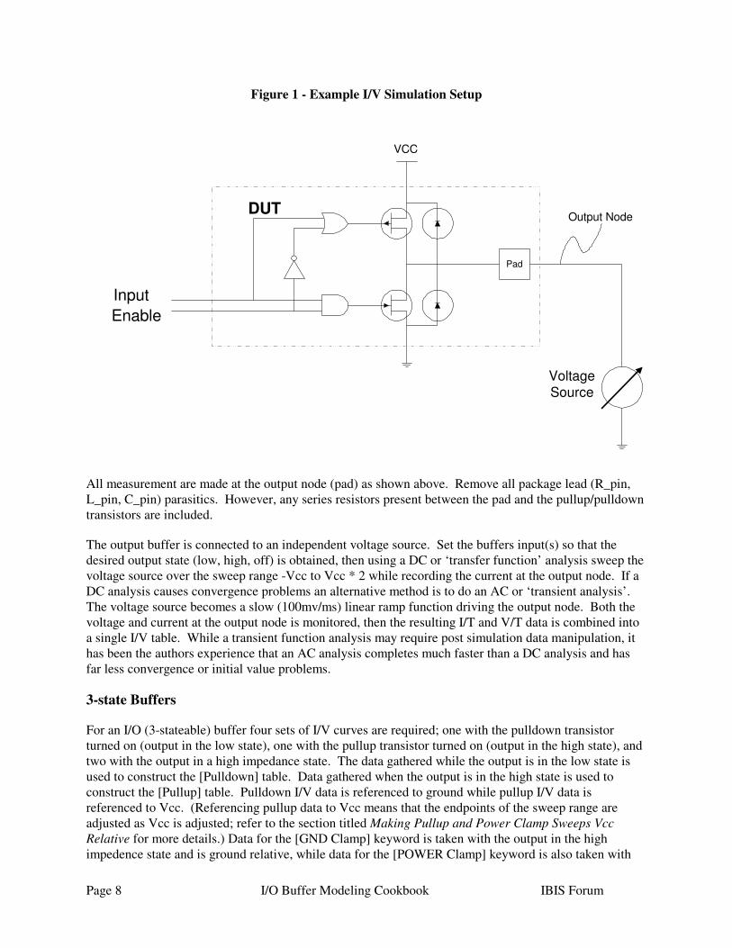
A typical simulation setup for an output or I/O buffer is shown in Figure 1 below. For this example the device under test (DUT) is a standard 3-state buffer with a single push-pull output stage.
Page 8 I/O Buffer Modeling Cookbook IBIS Forum
Figure 1 - Example I/V Simulation Setup
VCC
Pad
Input
DUT
VoltageSource
Enable
Output Node
All measurement are made at the output node (pad) as shown above. Remove all package lead (R_pin, L_pin, C_pin) parasitics. However, any series resistors present between the pad and the pullup/pulldown transistors are included.
The output buffer is connected to an independent voltage source. Set the buffers input(s) so that the desired output state (low, high, off) is obtained, then using a DC or ‘transfer function’ analysis sweep the voltage source over the sweep range -Vcc to Vcc * 2 while recording the current at the output node. If a DC analysis causes convergence problems an alternative method is to do an AC or ‘transient analysis’. The voltage source becomes a slow (100mv/ms) linear ramp function driving the output node. Both the voltage and current at the output node is monitored, then the resulting I/T and V/T data is combined into a single I/V table. While a transient function analysis may require post simulation data manipulation, it has been the authors experience that an AC analysis completes much faster than a DC analysis and has far less convergence or initial value problems.
3-state Buffers
For an I/O (3-stateable) buffer four sets of I/V curves are required; one with the pulldown transistor turned on (output in the low state), one with the pullup transistor turned on (output in the high state), and two with the output in a high impedance state. The data gathered while the output is in the low state is used to construct the [Pulldown] table. Data gathered when the output is in the high state is used to construct the [Pullup] table. Pulldown I/V data is referenced to ground while pullup I/V data is referenced to Vcc. (Referencing pullup data to Vcc means that the endpoints of the sweep range are adjusted as Vcc is adjusted; refer to the section titled Making Pullup and Power Clamp Sweeps Vcc Relative for more details.) Data for the [GND Clamp] keyword is taken with the output in the high impedence state and is ground relative, while data for the [POWER Clamp] keyword is also taken with
IBIS Forum I/O Buffer Modeling Cookbook Page 9
the output in a high impedance state but with the data Vcc relative. Each set of curves must be repeated under the minimum, typical and maximum corner conditions and must cover the entire sweep range. Thus, a buffer with 3-state capabilities would require the following 12 I/V data sets:
• Pulldown I/V under minimum, typical and maximum conditions, data ground relative
• Pullup I/V under minimum, typical and maximum conditions, data VCC relative
• High Impedance state I/V under minimum, typical and maximum conditions, data ground relative
• High Impedance state I/V under minimum, typical and maximum conditions, data VCC relative
Output Only Buffers
For a output only (non 3-state) output buffer only two sets of curves are needed; one with the pulldown transistor turned on (output in the low state), and one with the pullup transistor turned on (output in the high state). As before, pulldown I/V data is referenced to ground while pullup I/V data is referenced to Vcc. Because an output only buffer does not have a 3-state mode the power and ground clamp diode curves cannot be isolated from the transistor curves; the beyond the rail data is simply included in the pullup and pulldown I/V data. The [GND Clamp] and [POWER Clamp] keywords are not required for an output only buffer.
Open Drain Buffers
Open-drain or open-collector type devices only require three sets of I/V data: [Pulldown], [GND Clamp] and [POWER Clamp]. Data for the [Pulldown] table is gathered as described previously. [POWER Clamp] and [GND Clamp] data is gathered by turning off the pulldown transistor then doing the two I/V sweeps as described above for an I/O buffer in the high impedance state. Note that an open drain buffer may not require the full -Vcc to Vcc * 2 sweep range; refer to the section below entitled Sweep Ranges.
Input Buffers
When gathering I/V data for input buffers the same general setup is used, only the variable voltage source is placed on the input node. Input buffers require only [POWER Clamp] and [GND Clamp] I/V data. As with the output buffer, [GND Clamp] data is gathered via a voltage sweep with the voltage source referenced to ground and the [POWER Clamp] data is gathered by a voltage sweep with the voltage source Vcc relative. If an input device includes weak resistors to power or ground their I/V curves are included into the respective ground clamp or power clamp I/V data.
Sweep Ranges
As per the IBIS specification I/V data must be supplied over the range of voltages the output could possible see in a transmission line environment. Assuming that a devices’ output swings from ground to Vcc (where Vcc is the voltage given by the [Voltage Range] or [Pullup Reference] keywords) this range is -Vcc (the maximum negative reflection from a shorted transmission line) to Vcc *2 (the maximum positive reflection from an open circuited transmission line). However, be aware that if a device is operating in an environment where its output could be actively driven beyond these limits the I/V table must be extended further. Consider, for example, a 3.3v I/O buffer operating in a mixed 3.3v/5v system. While the devices output may only drive from 0 to 3.3v, a five volt device connected to this output may drive the output node beyond 3.3v volts. In this case I/V data should be supplied over a full -5v to +10v
Page 10 I/O Buffer Modeling Cookbook IBIS Forum
rang. Likewise, an open collector or open drain device may be terminated in a voltage (Vpulllup) different than that given by the [Voltage Range] keyword. In this case it is permissible to supply the pullup and pulldown data over the range -Vpullup to Vpullup *2.
It is recognized that semi-conductor device models may not be well behaved over these ranges, so it is acceptable to lessen the actual sweep range then use linear extrapolation to get to the required endpoints. For example, suppose one were attempting to gather the I/V data for a typical 5v device. The IBIS specification requires I/V data over the full -5v to 10v range. The model maker may choose to limit the simulation sweep to -2v to +7v, and then extrapolate to the final -5v to +10v range. Be aware however, that the simulation sweep range must be enough to forward bias any ESD/protection diodes or the diodes intrinsic to the output transistor structures.
Making Pullup and Power Clamp Sweeps Vcc Relative
As stated earlier the pullup and power clamp data is relative to Vcc. In order to make the pullup and power clamp data Vcc relative (and to enter this I/V data into IBIS’s table format properly) adjust the starting and ending endpoints of these sweep to follow the variations in Vcc. For example, suppose one where gathering the pullup data for a standard 3.3v device whose Vcc specification was 3.3v +/- 10% (i.e. the operating Vcc ranged from 3.0v minimum to 3.6v maximum). The sweep voltage under typical conditions would range from -3.3 V to +6.6 V. For minimum conditions, where the VCC was adjusted to 3.0 V, the sweep voltage should also be adjusted negative 0.3 V, to sweep from -3.6V to +6.3V. Likewise, for maximum conditions, adjust the sweep endpoint positive 0.3v so the sweep covers -3.0v to 6.9v. By gathering the data in this manner the corresponding voltage data point in all three data sets represent the same ‘distance’ from Vcc. Note that the 9.9v sweep RANGE remains the same for all three simulations.
Diode Models
When doing digital I/O buffer designs most of the analysis is concerned with the buffer’s Tco parameter and output impedance. Very little attention is paid to a buffers ‘beyond the rail’ operation. Thus, the diode models included in buffer’s schematic may be included for layout or completeness only, and are most likely ‘perfect’ diodes with no intrinsic resistance. Likewise, if the design relies on the intrinsic diode structure of the output transistors to provide output protection the transistor models may not properly model this mode of operation. Therefore, when doing simulation in these voltage regions one may get unrealistically large (K amp) power and ground clamp currents. If this is a problem the model creator has a couple of options. Working with the buffer designer the diode or transistor models can be enhanced to include the proper junction or bulk resistance. Note that with large ESD structures the metal resistance can be relatively large -- on the order of a few ohms – an this should be included in the design. If an actual device is available the model creator can measure the power and ground clamp I/V data directly.
Diode Transient Time Data
This section is still under construction
IBIS Forum I/O Buffer Modeling Cookbook Page 11
3.2.2 Extracting the Ramp Rate or V/T Waveform Data
Simulations to obtain the ramp rate and/or V/T (output voltage vs. Time) curves are relatively straight forward. For each simulation corner (minimum, typical, maximum) two V/T data sets are required; one for the buffer output switching low to high, the other is for the buffer output switching high to low. This data can then be reported as a rising and falling dv/dt ratios (the ‘ramp rate’) or the actual V/T data may be reported directly.
Extracting Data for the [Ramp] Keyword
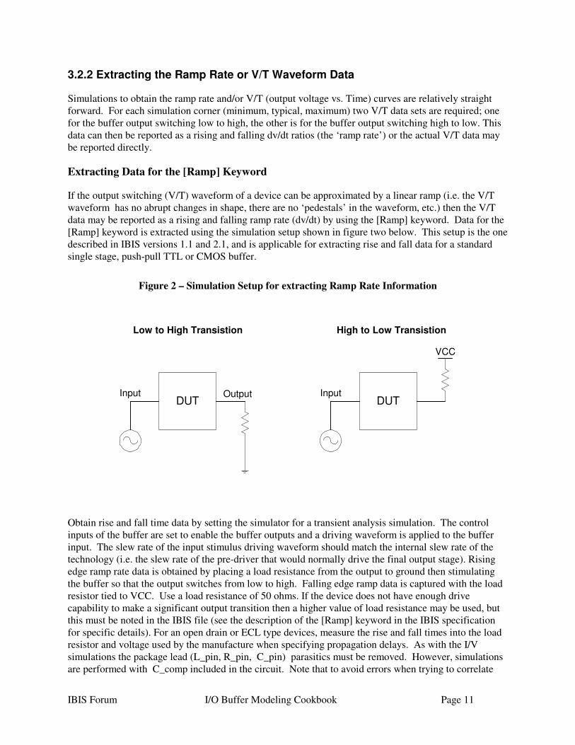
If the output switching (V/T) waveform of a device can be approximated by a linear ramp (i.e. the V/T waveform has no abrupt changes in shape, there are no ‘pedestals’ in the waveform, etc.) then the V/T data may be reported as a rising and falling ramp rate (dv/dt) by using the [Ramp] keyword. Data for the [Ramp] keyword is extracted using the simulation setup shown in figure two below. This setup is the one described in IBIS versions 1.1 and 2.1, and is applicable for extracting rise and fall data for a standard single stage, push-pull TTL or CMOS buffer.
Figure 2 – Simulation Setup for extracting Ramp Rate Information
OutputDUT
InputDUT
Input
VCC
Low to High Transistion High to Low Transistion
Obtain rise and fall time data by setting the simulator for a transient analysis simulation. The control inputs of the buffer are set to enable the buffer outputs and a driving waveform is applied to the buffer input. The slew rate of the input stimulus driving waveform should match the internal slew rate of the technology (i.e. the slew rate of the pre-driver that would normally drive the final output stage). Rising edge ramp rate data is obtained by placing a load resistance from the output to ground then stimulating the buffer so that the output switches from low to high. Falling edge ramp data is captured with the load resistor tied to VCC. Use a load resistance of 50 ohms. If the device does not have enough drive capability to make a significant output transition then a higher value of load resistance may be used, but this must be noted in the IBIS file (see the description of the [Ramp] keyword in the IBIS specification for specific details). For an open drain or ECL type devices, measure the rise and fall times into the load resistor and voltage used by the manufacture when specifying propagation delays. As with the I/V simulations the package lead (L_pin, R_pin, C_pin) parasitics must be removed. However, simulations are performed with C_comp included in the circuit. Note that to avoid errors when trying to correlate
Page 12 I/O Buffer Modeling Cookbook IBIS Forum
later simulations with those used to extract rise/fall time information, use the same "time step" throughout the simulation and correlation procedure.
Extracting Data for the Rising and Falling Waveform Keywords
In IBIS version 2.1 V/T data may be reported directly by using the [Rising Waveform] and [Falling Waveform] keywords. These two keywords are generally required if the output switching waveform of the device is significantly non-linear (this is the case with most ‘controlled rise time’ or ‘graduated turn on’ style buffers). The use of these keywords is also indicated if the device incorporates a delay between the turning off of one output transistor and the turning on of the other (i.e. the V/T waveform contains a pedestal). Finally, the model creator may wish to include the V/T data directly so that the model itself includes it own verification feature. By including this ‘golden waveform’ the model user may perform a simulation with the buffer driving the same load as was used to generate the V/T waveforms. The results of this simulation should match the V/T waveform as given in the IBIS file, thereby verifying that the users simulator is producing the proper results.
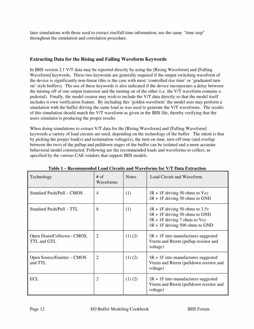
When doing simulations to extract V/T data for the [Rising Waveform] and [Falling Waveform] keywords a variety of load circuits are used, depending on the technology of the buffer. The intent is that by picking the proper load(s) and termination voltage(s), the turn-on time, turn-off time (and overlap between the two) of the pullup and pulldown stages of the buffer can be isolated and a more accurate behavioral model constructed. Following are the recommended loads and waveforms to collect, as specified by the various CAE vendors that support IBIS models.
Table 1 – Recommended Load Circuits and Waveforms for V/T Data Extraction
Technology # of Waveforms
Notes Load Circuit and Waveform
Standard Push/Pull – CMOS 4 (1) 1R + 1F driving 50 ohms to Vcc 1R + 1F driving 50 ohms to GND
Standard Push/Pull – TTL 8 (1) 1R + 1F driving 50 ohms to 3.5v 1R + 1F driving 50 ohms to GND 1R + 1F driving 7 ohms to Vcc 1R + 1F driving 500 ohms to GND
Open Drain/Collector– CMOS, TTL and GTL
2 (1) (2) 1R + 1F into manufactures suggested Vterm and Rterm (pullup resistor and voltage)
Open Source/Emitter – CMOS and TTL
2 (1) (2) 1R + 1F into manufactures suggested Vterm and Rterm (pulldown resistor and voltage)
ECL 2 (1) (2) 1R + 1F into manufactures suggested Vterm and Rterm (pulldown resistor and voltage)
IBIS Forum I/O Buffer Modeling Cookbook Page 13
Note: (1) 1R = one rising waveform, 1F = one falling waveform (2) if recommended termination resistor is >100 ohms, include 1R +1F driving 50 ohms to Vterm
Note: Be aware that not all CAE vendors’ simulation software will use all the given waveforms. If in doubt, check with your CAE vendor.
As with the simulations for ramp rate the slew rate of the driving waveform should match the internal slew rate of the technology. For meaningful results all of the above rising and falling waveforms should be taken with the package lead parameters (R_pin, L_pin, C_pin) and fixture reactive elements (L_fixture and C_fixture) set to zero. (The L_fixture and C_fixture parameters are included as parameters of the [Rising Waveform] and [Falling Waveform] keywords only for use in documenting a measurement setup or creating complex loads for simulator comparison and validation via a golden waveform.) As noted in the IBIS specification itself, it is critical that all rising and falling waveforms be time correlated. In other words, the rising (falling) edge data in each of the rising (falling) edge waveform tables must be entered with respect to a common reference point on the input waveform used to stimulate the buffer.
In addition to the above recommended V/T waveforms, additional waveforms may be included for simulator validation purposes. These waveforms are referred to as ‘golden waveforms’ because their intent is to supply a reference waveform that the simulator attempts to match, not raw V/T data that the simulator uses to construct the behavioral model. Unlike the recommend loads above, the load circuits used to generate golden waveforms can include reactive elements. Two popular golden wavefrom loads are 50 ohms to (Vcc - GND) / 2, and a 50pf load to ground. The model maker may also wish to include a waveform of the buffer driving a load that represents the typical load found in the buffers intended application.
Finally, some devices may show slightly different rising and falling edge characteristics depending on how much time the buffer has had to settle from a previous output transition. Some projects may ask that the model creator extract ramp or V/T data from the second or third output transition in a series.
Minimum Time Step
As a rule of thumb, set the minimum time step so that there are between 30 to 50 data points in a rising or falling V/T curve. If the V/T waveform is especially complex more points may be required (note however that the V/T waveform tables can contain no more than 100 points). If the data is going to be reduces to a dv/dt under the [Ramp] keyword then fewer points may be required.
Multi State Drivers
This section is still under construction.
3.3 Obtaining I/V and Switching Information via Lab Measurment
You can obtain I-V curves and rise/fall time information from the actual IC, using the following lab setup:
Page 14 I/O Buffer Modeling Cookbook IBIS Forum
• A programmable power supply with an output capable of sinking and sourcing current while maintaining the required output voltage. The output must be floating.
• A curve tracer
• A digital sampling oscilloscope with at least a 4 GHz bandwidth
• A low capacitance probe, e.g. FET
• A test fixture used for DC measurements
• A motherboard or specific test fixture used for AC measurements
• If available, a thermoelectronic hot/cold plate (a peltier device), to control die temperature
To obtain I-V curve measurements, mount the device under test (DUT) in the DC test fixture and connect the power and ground pins of the DUT to the programmable power supply. Attach the hot/cold plate to the device with a very thin layer of thermal grease and adjust the temperature as desired. Wait for the die to stabilize at the desired temperature. Select an output on the DUT in the desired state (high or low) and use the curve tracer to obtain the I-V characteristics of the output.
Notes During curve tracing of a tri-statable output, the curve contains both the transistor and the diode output characteristics. To obtain curves for the diodes alone, select and curve trace the output in its high impedance state.
Devices containing time-delayed feedback can produce bad results.
Reference the pullup and power clamp data to VCC, as described in the IBIS specification. You can obtain this data directly by connecting the curve tracer's negative (reference) lead to the VCC supply of the DUT, then setting the curve tracer for a negative sweep. Make sure no ground path connects back through the AC line between the device ground and power supply ground. For standard pulldown and clamp diode curves, attach the negative lead to the DUT's GND supply and use a positive sweep direction. Ensure the supply is floating.
Note that the curve tracer may not be able to sweep the entire range required by the IBIS specifcation. In this case the model creator must extrapolate the curves to the required range.
Capturing rise/fall time data requires either a specific test fixture or a motherboard to which the DUT can be attached. Rise/fall time measurements require an oscilloscope with at least a 4 GHz bandwidth. Take into account the effect on the rise/fall times of the device packaging and capacitive load. Use a probe with extremely low loading, i.e. 1 pf or less, such as a FET probe. The probe grounding should be less than 0.5 inches; i.e., don't use the standard 6 inch probe grounds.
Take an oscilloscope picture of a buffer driving a known load. Then, using the known packaging parameters and measured I-V curves, construct a simulation model of the device using a best guess of the rise/fall time. With an IBIS simulator, adjust the rise/fall times in the model until the simulation results match the oscilloscope waveforms. For greater control, lift the pin under test from any load other than the scope probe and simulate with a package and probe model.
IBIS Forum I/O Buffer Modeling Cookbook Page 15
4.0 Putting the Data Into an IBIS File Once the I/V and switching information for a components buffers has been obtained, this data is put into an IBIS file. This file has a specific format as described in the IBIS specification. The purpose of this chapter is to give the model creator pointers on how to construct this file.
An IBIS file consists of three parts, with an optional ‘external’ package description. The three parts consist of
1. general information about the file itself and the component being modeled
2. the components name, pin-out and pin-to-buffer mapping
3. and finally, a behavioral descriptions of each unique buffer type in that component.
Note that an IBIS file can contain a description of more than one component (i.e. parts 2 and 3 can be repeated several times within one IBIS text file). For more information refer to the description of the [Component] keyword in the specification.
4.1 IBIS File Header Information
The first section of an IBIS file contains basic information about the file itself and the data in it. This section includes the following keywords:
Keyword Required? Description
[IBIS Ver] Yes What version of IBIS this file uses.
[Comment char] No Change the comment character. By default it’s the pipe (|) character
[File Name] Yes Name of this file. Remember that all file names must be lower case and conform to the DOS 8.3 convention. The file name extension for an IBIS file is .ibs
[File Rev] Yes The revision level of this file (or model). The specification contains a guidelines for assigning revision levels.
[Date] No Date this file was created
[Source] No The source of the data in this file. Is it from a data book? Simulation data? Measurement?
[Notes] No Component or file specific notes. Please see the discussion below.
[Disclaimer] No May be legally required
[Copyright] No The files copyright notice
Page 16 I/O Buffer Modeling Cookbook IBIS Forum
The use of these keywords is pretty self explanatory. Note that while the [Date], [Source], etc. keywords are not required, there use is strongly recommended. The [Notes] keyword is especially valuable, in that the model creator can include in the IBIS file such information as:
• Specific model and simulator use information. For example, if the file is marked as IBIS revision 2.1 the [Notes] keyword may specify what specific 2.1 features a simulator must support. Specific model use requirements or caveats may also be described here.
• Information on SSO conditions. Under what switching conditions (i.e. how many SSO’s) were the minimum, typical and maximum corners derived. Was the devices Tco taken under the same conditions (it should be).
• Additional package modeling information may be included
• The models validation level may also be described
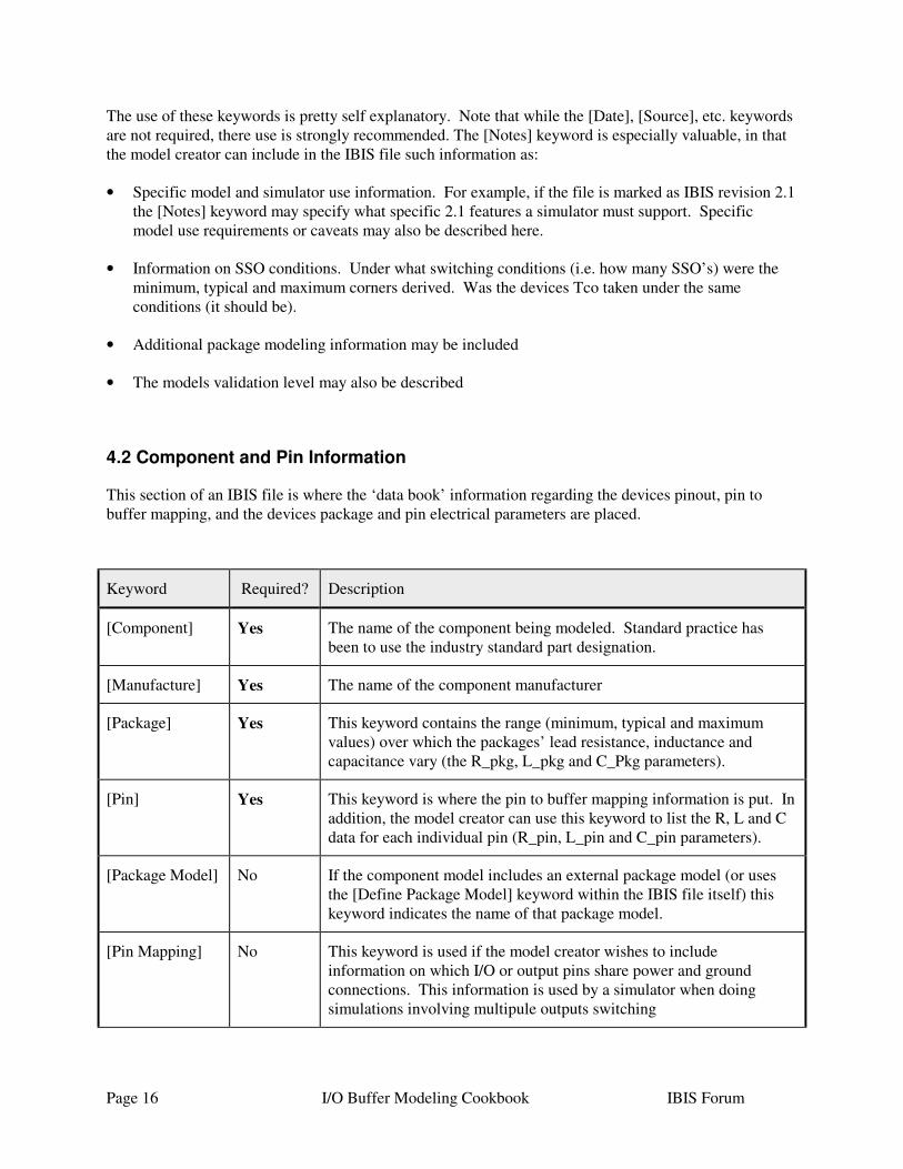
4.2 Component and Pin Information
This section of an IBIS file is where the ‘data book’ information regarding the devices pinout, pin to buffer mapping, and the devices package and pin electrical parameters are placed.
Keyword Required? Description
[Component] Yes The name of the component being modeled. Standard practice has been to use the industry standard part designation.
[Manufacture] Yes The name of the component manufacturer
[Package] Yes This keyword contains the range (minimum, typical and maximum values) over which the packages’ lead resistance, inductance and capacitance vary (the R_pkg, L_pkg and C_Pkg parameters).
[Pin] Yes This keyword is where the pin to buffer mapping information is put. In addition, the model creator can use this keyword to list the R, L and C data for each individual pin (R_pin, L_pin and C_pin parameters).
[Package Model] No If the component model includes an external package model (or uses the [Define Package Model] keyword within the IBIS file itself) this keyword indicates the name of that package model.
[Pin Mapping] No This keyword is used if the model creator wishes to include information on which I/O or output pins share power and ground connections. This information is used by a simulator when doing simulations involving multipule outputs switching
IBIS Forum I/O Buffer Modeling Cookbook Page 17
[Diff Pin] No This keyword is used only if the component contains differential pins.
Again, these keywords are pretty well explained in the specification. Note that for most components the required keywords [Component], [Manufacturer], [Package] and [Pin] are all that are needed to build the model. The [Pin] keyword is where the pins of the device are defined, and each of the buffer models created are mapped to specific pins. As described in the specification, there must be a buffer model (as called out by the [Model] keyword) for each non power/ground/no-connect pin.
R_pkg, L_pkg and C_pkg are the overall (min and max) values of the packages lead resistance, inductance and capacitance. The numerically largest values of R, L and C are listed as the ‘max’ values, while the numerically smallest values of R, L and C are listed as the ‘min’ values.
Note the [Pin Mapping] keyword. If a particular buffer model is intended to represent that buffer in isolation, then the [Pin Mapping] keyword can be used to gang several buffers together in order to perform a simulation that includes the effects of multiple outputs switching. If the model is intended to be used with the [Pin Mapping] keyword information then that should be noted in the [Notes] section. Note however that not all simulators support this feature.
4.3 The [Model] Keyword
The [Model] keyword starts the description of the data for a particular buffer. While a buffer model can appear quite complex, most buffers can be described using just a few of the parameters and keywords.
Parameter section
A model description starts with the user specifying a few basic parameters. These parameters tell the simulator what type of buffer the model represents, and some ‘data book’ characteristics of the buffer that enable simulators to do automatic error checking.
[Model] Parameter Required Description
Model_Type Yes Defines the type of buffer (input, output, I/O, etc.)
Polarity No The polarity of the signals driven by this buffer (high true or low true).
Enable No The polarity of this buffers output enable signal (if applicable)
Vinl, Vinh No The buffers input logic thresholds
C_Comp Yes Buffers input or output capacitance. Note the discussion on ‘min’ and ‘max’ values of C_comp included in the text below.
Page 18 I/O Buffer Modeling Cookbook IBIS Forum
Vmeas, Cref, Rref, Vref No Provides the simulator with this buffers Tco measurement conditions
The IBIS specification gives an extensive list of possible buffer types. Peruse this list carefully to choose your buffer type. Note that if an input or I/O buffer type is chosen the user must specify the Vinl and Vinh parameters or verify that the IBIS defaults are correct. The Vinl and Vinh parameter are included so that simulators can flag signal integrity violations and perform timing calculations. In addition, all output or I/O type buffer models should include the Vmeas, Cref, Rfer and Vref parameters. Including these parameters allows a simulator to do board level timing calculations.
The C_comp parameter specifies the buffers input, output or I/O capacitance and can have a typical, minimum and maximum value. Note that when constructing the IBIS file the numerically largest value of C_comp is listed as the ‘max’ value while the numerically smallest value of C_comp is listed as the ‘min’ value. C_Comp min and max values do not necessarily correlate with the min and max conditions under which the I/V and switching data was gathered.
Temperature and Voltage Keywords
Once the basic buffer type and data book parameters have been specified the temperature and voltage ranges over which the device operates is given by the following keywords.
Keyword Required? Description
[Temperature Range]
No The temperature range over which the min, typ and max I/V and switching data has been gathered. If not specified then 0, 50 and 100 degrees C is assumed.
[Voltage Range] Yes The range over which Vcc is varied to obtain the min, typ and max pullup and power clamp data.
[Pullup Reference]
[Pulldown Reference]
[POWER Clamp Reference]
[GND Clamp Reference]
No Allows the user to specify alternate references (i.e. voltage rails) for any of the four I/V curves.
IBIS Forum I/O Buffer Modeling Cookbook Page 19
The [Temperature Range] keyword is pretty self explanatory. Note that the ‘min’ and ‘max’ temperature values listed in an IBIS file correspond to the conditions under which the ‘min’ and ‘max’ I/V and switching data was taken. For example, if the minimum (weakest drive, slowest edge) data was taken at 85 degrees C, and the maximum data were taken at 0 degrees C, then ’85’ would be entered in the ‘min’ column and 0 would be entered into the ‘max’ column.
The [Voltage Range] keyword specifies the range over which Vcc is varied to obtain the min, typ and max conditions. In addition, this keyword supplies the default voltage reference value for the pullup and power clamp I/V curves. Normally, the [Voltage Range] keyword is all that is required. However, if a buffer uses multiple power supply rails the alternate keywords are used. Very specifically, if the model creator gathers pullup or power clamp I/V data using a voltage reference other than that called out by the Vcc keyword, then the [Pullup Reference] or [POWER Clamp Reference] keywords are used. Use of these keywords is probably best shown by example.
I/V data section
Once the voltage references have been established the I/V data can be entered via the four I/V data keywords shown below:
Keyword Required? Description
[Pulldown] No Data gathered while an output or I/O buffer is in the logic low state is entered here. This keyword is not used for input buffers.
[Pullup] No Data gathered while an output or I/O buffer is in the logic high state is entered here. This keyword is not used for input buffers.
[GND Clamp] No IV curve when the input or output of a buffer is driven below ground (or the reference specified by the [GND Clamp Reference] keyword
[POWER Clamp] No IV curve when the input or output of a buffer is driven above Vcc (or the reference specified by the [POWER Clamp Reference] keyword
The first thing one notices is that, strictly speaking, none of the four I/V curves are mandatory. Non 3-state buffers (i.e. buffers where one cannot isolate separate power and ground clamp diode effect) require only the [Pulldown] and [Pullup] keywords. Input buffers use only the [GND Clamp] and [POWER Clamp] keywords. 3-state buffers require all four keywords. Open drain/collector buffers can make the current data in the [Pullup] table all zeros, or omit the [Pullup] keyword altogether.
Each keyword is followed by a set of data in tabular format. Enter the gathered I-V data into the appropriate tables The rules for constructing the I-V tables are as follows:
Pulldown
Enter into the [Pulldown] table the I/V data gathered while the output or I/O buffer was in the logic low state. Pulldown data must cover the range of -Vcc to Vcc *2. If the buffer is a 3-state device then first subtract the ground clamp current from the pulldown current then enter the result into the [Pulldown] table. Note that this will result in a pulldown I/V curve that resembles the curve below:
Page 20 I/O Buffer Modeling Cookbook IBIS Forum
V
I
Pullup I/V curve after subtraction of ground clamp currents
Below zero volts the buffers current starts to increase (become more negative), but then heads back towards zero. While this looks odd, it is OK. When doing simulation with the buffer in it’s active state a simulator sums the ground clamp I/V curve with the pulldown I/V curve to arrive back at the original pulldown I/V curve.
Ground Clamp
Enter into the [GND Clamp] table the ground clamp I/V data. For I/O buffers this is the ground relative data gathered while the buffer was in the high impedance state. The data in table must cover the range of -Vcc to Vcc.
Pullup
Enter into the [Pullup] table the data gathered while the output or I/O buffer was in the logic high state. Again, if the buffer is a 3-state device then first subtract the power clamp current from the pullup current then enter the result into the [Pullup] table. Pullup data must cover the range -Vcc to Vcc *2. As per the specification, the voltage points are entered into the table using the formula:
Vtable = VCC - Voutput
For example, for a standard 5v device the numerical values for voltage listed in the table range from +15v (when the output is 5v below ground) to -5v (when the output is 5v above Vcc).
IBIS Forum I/O Buffer Modeling Cookbook Page 21
Power Clamp
Finally, enter into the [POWER Clamp] data the power clamp I/V data. For I/O buffers this is the Vcc relative data gathered while the buffer was in the high impedence state. The data in the table must cover the range of Vcc to Vcc *2.
Extrapolation Errors
One common error when building clamp tables involves extrapolation errors on the last data point. Most simulators extrapolate the last two data points in a table to calculate values beyond the table's range. Therefore, be sure that all curves going to zero have the last two data points as zero. As an example, the incorrect way to enter a diode curve is:
Voltage Current 0.0 V 0 mA 0.6 V 2 mA
With the above, a simulator assumes a -2 mA current through the diode at -.6 V bias. The correct way to enter the curve is:
Voltage Current 0.0 V 0 mA 0.4 V 0 mA 0.6 V 2 mA
With this table, the simulator extrapolates the diode curve correctly.
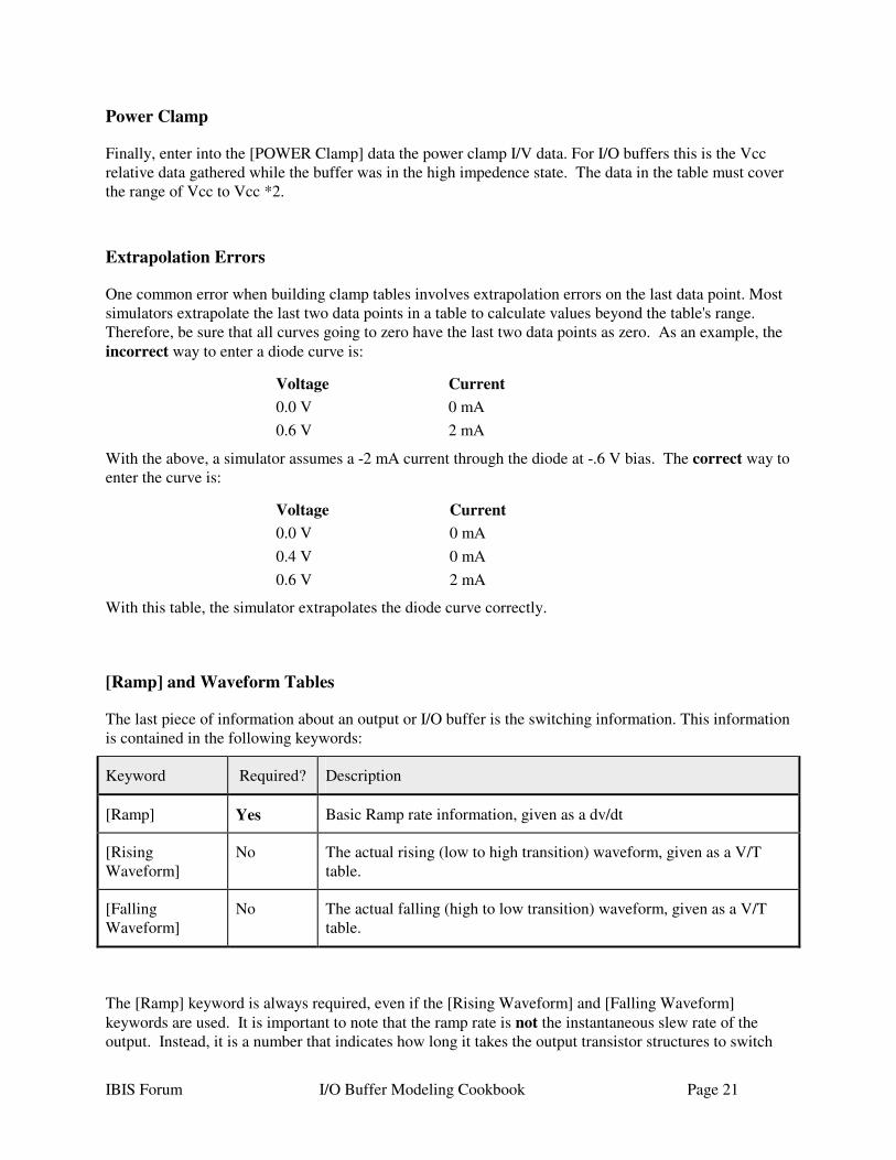
[Ramp] and Waveform Tables
The last piece of information about an output or I/O buffer is the switching information. This information is contained in the following keywords:
Keyword Required? Description
[Ramp] Yes Basic Ramp rate information, given as a dv/dt
[Rising Waveform]
No The actual rising (low to high transition) waveform, given as a V/T table.
[Falling Waveform]
No The actual falling (high to low transition) waveform, given as a V/T table.
The [Ramp] keyword is always required, even if the [Rising Waveform] and [Falling Waveform] keywords are used. It is important to note that the ramp rate is not the instantaneous slew rate of the output. Instead, it is a number that indicates how long it takes the output transistor structures to switch
Page 22 I/O Buffer Modeling Cookbook IBIS Forum
from one state to another. As such, the dv portion of the [Ramp] keyword data is specified to cover the 20% to 80% voltage swing of the output. Specifically, the "ramp rate" as posted in an IBIS file is defined as:
dvdt
to voltage swingTime it takes to swing the above voltage
= 20 80% %
Do not reduce dv/dt to a single number.
4.4 External Package Models
This section is still under construction
4.5 Verifying the IBIS file
After creating an IBIS file, check it for correct construction and syntax. A program called "ibischk2" is used to verify the IBIS file. This program (the golden parser) is also available from the IBIS Open Forum (see the section titled Resources). The golden parser is available for a variety of hardware platforms and operating systems.
To run the golden parser at the prompt, type:
ibischk2 <filename>
Note There are two versions of this program: one for DOS based systems and one for UNIX based systems. Because of the differences in line feed/carriage return characters in DOS and UNIX, an IBIS file created with a DOS text editor can fail when checked with the UNIX version of the program. Utilities such as "dos2unix" and "unix2dos" are available to convert between the DOS and UNIX texts.
IBIS Forum I/O Buffer Modeling Cookbook Page 23
5.0 Validating the Model Once an IBIS model has been created, it must be validated. Validation involves
1. From the IBIS data, creating a behavioral simulation model in a target simulator that supports IBIS.
2. Running the model with standard loads.
3. Comparing the results against a transistor-level reference simulation using the same loads.
You can use any simulator that supports IBIS. Contact the simulator vendor and request their parser, converter, or application note on using IBIS models on their tools. To find simulator vendors that support IBIS, see the IBIS member list maintained in the "vhdl.org" archives.
Page 24 I/O Buffer Modeling Cookbook IBIS Forum
6.0 Correlating the Data The last step in the modeling process is to correlate the simulation results with actual silicon measurements. To obtain I-V curves and rise/fall time measurements, see the section titled Obtaining Curves by Lab Measurement of Silicon.
Correlation involves measuring the I-V curves and rise/fall times of an actual IC and verifying that they fall within the maximum and minimum values used in the IBIS model. In addition, for ICs in a motherboard or other test setup driving a known load, compare the oscilloscope waveforms with simulation waveforms using the same load.
Note The oscilloscope adds a load to the circuit and the response of the oscilloscope affects the response measured.
IBIS Forum I/O Buffer Modeling Cookbook Page 25
7.0 Resources The IBIS Open Forum is a working group of the EIA association, and as such is responsible for the official IBIS specification. Minutes of IBIS meetings, email correspondence, proposals for specification changes, etc. are on-line at "eia.org". To join in the email discussions, send a message to "[email protected]" and request that your name be added to the IBIS mail reflector. Be sure to include your email address.
To download a copy of the specification, the golden parser, various public-domain models, s2ibis program, the IBIS Overview in PostScript, and other information, visit the IBIS Web page.
WWW: http://www.eia.org/eig/ibis/ibis.htm
FTP: (IP address 198.31.14.3) login as "anonymous" password is your email address
IBIS-related files are in the directory "/pub/ibis" and its subdirectories.
To get documents by email, send an email message to "[email protected]" with the following commands in the message body:
For Internet access, use "ftp vhdl.org" (or "ftp 198.31.14.3") and log in as user "anonymous". The gopher utility is available and highly recommended. Gopher to "vhdl.org". Set "binary" mode for transferring binary files (*.doc, *.fm, *.xls).
Page 26 I/O Buffer Modeling Cookbook IBIS Forum
Example 1 – Basic (Version 1.1) model Following is an example IBIS model of an industry standard hex inverter (74HC04). This example shows the use of the required IBIS keywords and the modeling of input and output buffers
Example 2 – Version 2.1 model of a Multi-supply PCI component This example should show the use of the voltage reference keywords. This example should also include 3-state buffers.
Example 3 – An Open Drain, Controlled Rise time (GTL) Model This example shows how to model an open drain device, as well as the use of the [Rising Waveform] and [Falling Waveform] keywords
Example 4 – A device with differential pins This example should show the use of the [Diff Pin] keyword
Example 5 – ECL devices This example should show how to model an ECL component.