12
JANUARY 2015 CAPABILITIES + DESIGN SOLUTIONS GUIDE IC-TO-BOARD

JANUARY 2015
CAPABILITIES + DESIGN SOLUTIONS GUIDEIC-TO-BOARD

2
Advanced IC Packaging
FLIP CHIP AND UNDERFILL
DAM AND ENCAPSULATION
FINE PITCH WIREBOND
PRECISION DIE ATTACH
Micro Interposers
PROFILE AND PITCH FLEXIBILITYULTRA HIGH DENSITYTERMINATION
FLEXIBILITYULTRA LOW PROFILE
Samtec combines Advanced IC Packaging and Ultra Micro Interposer technologies to achieve optimized interconnect paths - from the bare die to an interface 100 meters away, and all insertion points in between - with expertise in:
– Package and substrate design
– System modeling and prototyping
– Assembly and electrical testing of finished goods
– Ultra low profile, high density and dual compression contact micro interposers
– Advanced IC packaging, including die attach, wirebond, flip chip, dam and encapsulation, and micro optics
Samtec offers end-to-end signal integrity support including full channel analysis, high data rate simulations, break out routing and application assistance.
Visit SamtecMicroelectronics.com or contact the Microelectronics Group at [email protected].
END-TO-END SYSTEM DESIGN + CAPABILITIES
ADVANCED IC PACKAGING+
MICRO INTERPOSERS
STREAMLINED INTERCONNECT PATH

54 4
MICRO INTERPOSERS
Samtec’s Z-Ray™ micro array interposers are ultra low profile, ultra high density, and highly customizable solutions ideal for complex IC-to-Board applications.
– Ultra low profile, high density arrays, with BeCu micro-formed contacts on 0,80 mm and 1,00 mm pitches
– Ultra flexible, with a variety of standard and custom configurations, including dual compression, solder ball, and an array of sizes and shapes
– Assembled into rugged low profile FR4 substrate under high pressure and temperature
– Choice of fastener options, including application specific designs, screw downs, quick install (easy on/off) and thermal spreaders
Contact [email protected] for more information.
END-TO-END SYSTEM DESIGN + CAPABILITIES
STANDARD & CUSTOM Z-RAY™ MICRO INTERPOSER CAPABILITIES
Series ZA8 ZA1 Capabilities
Pitch 0,80 mm 1,00 mm > 0,65 mm
Stack Height 1,00 mm 0,50 mm to 4,00 mm
Total I/Os 100 - 400 1,000+
Ruggedizing Screw Down Holes, Alignment Holes
Latches, Thermal Spreaders, Quick-Release Spring Constraints
Construction Single Layer FR4 Multi-layer FR4 (e.g., Pitch Spreaders)
Terminations Dual Compression, Compression + Solder Ball
TM
Z-Ray™ Ultra Low Profile Interposers
ULTRA HIGH DENSITY
Choice of 0,80 or 1,00 mm pitch grid
ZA8 Series for up to 1,200 contacts / in2
ZA1 Series for up to 1,024 contacts / in2
ULTRA LOW PROFILE
One piece design
Low profile 1,00 mm body height
Low 25 g of normal force with .008" (0,20 mm) contact deflection
ULTRA FLEXIBLE
Customer-specific stack heights, pin counts, pitches, shapes and plating thicknesses
Alignment and fastener options
Customizable in X-Y-Z axes
Quick-turn customizations with minimal NRE and tooling charges
Also Available & In Development
ULTRA HIGH DENSITY
Z-Ray™ on 0,635 mm pitch and 1000+ I/Os in development
MULTI-LAYER SYSTEM
Pitch spreaders and other embedded interconnect circuitry
MICRO COAX CABLES
34 AWG micro twinax cable on 0,80 mm pitch, 8 and 16 pairs standard

54
ZA1 Series [Actual Size]
ZA8 Series [Actual Size]
1,00 mm pitch with up to 1,024 contacts per square inch
Fastener options
0,80 mm pitch with up to 1,200 contacts
per square inch
Ultra low profile 1,00 mm body height
Adhesive-bonded cover film
Etched Ni & Au plated contacts
Adhesive-bonded formed BeCu
Cu plated through-hole in PCB core
Dual compression contact system
Single compression with solder balls
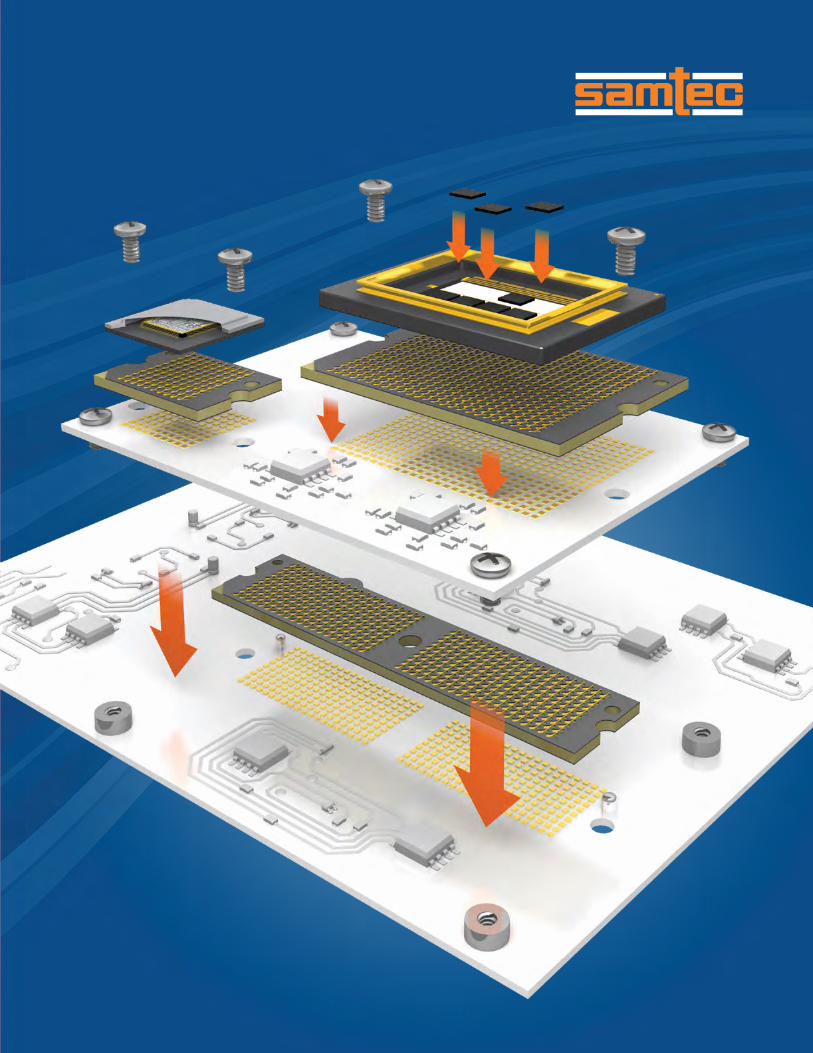
save PCB real estate • reduce cost • eliminate reworks & scrap • gain design flexibilityMODULARIZATION WITH Z-RAY™

6
ADVANCED IC PACKAGING
Samtec Microelectronics Group is positioned to provide you with complete signal chain support - from custom package and substrate design, to connector and cable selection, through signal integrity testing and debug of your full system - helping you ensure an optimized signal path.
– Advanced IC package and substrate design – Flip chip, die attach, wirebond, dam, encapsulation and lid attach – Modeling and prototyping – Testing and debug – In-house optical engine design, manufacturing and packaging
Samtec’s worldwide Signal Integrity Group is dedicated to helping you determine and implement the most streamlined signal path possible, with support including full channel analysis, high data rate simulation, break out region design and routing, interconnect selection and application assistance. Visit SamtecMicroelectronics.com for more information, or contact the Microelectronics or Signal Integrity Groups directly at [email protected] or [email protected].
DESIGN, MANUFACTURING AND SUPPORT
Complex Package Assembly
FLIP CHIP & UNDERFILL PRECISION DIE ATTACH
FINE PITCH & LOW PROFILE WIREBOND DAM, ENCAPSULATION & LID ATTACH

Full signal chain support
Interposer integration
Flip chip & underfill
Fine pitch and low profile wirebond
Precision die attach
PCB design with signal integrity support
Dam, encapsulation and lid attach
Custom package design & assembly
MICRO OPTICS DESIGN & PACKAGINGon-board & mid-board engines • high speed micro flyover • future-proof & equalized copper • [email protected]
Engine miniaturization

8
INDUSTRY-SPECIFIC APPLICATIONS
Samtec Microelectronics Group is positioned to support many industry-specific IC packaging applications. We provide leading-edge technologies and on-going development to ensure we are on the forefront of advanced IC packaging design and manufacturing.
Our manufacturing facility in Colorado Springs, Colorado, supports all areas of advanced IC packaging design, assembly, testing and manufacturing. Our technologies are supported by a reliable and accessible manufacturing infrastructure, along with full in-house signal integrity and system support.
Samtec adheres to a number of industry standard certifications and practices, including: – TS 16949 – ISO 9001 – ISO/TS Quality Manual – Environmental Compliance (RoHS) – MIL-STD-883 – ITAR Regulation Compliance
Visit SamtecMicroelectronics.com for more information, or contact the Microelectronics or Signal Integrity Groups directly at [email protected] or [email protected].
LEADING-EDGE TECHNOLOGIES + CONTINUOUS INNOVATION
MEDICAL & HEALTHCARE
Technologies / Capabilities – MEMs – Image packaging – Custom IC package design – Stacked and custom die – Chip-scale interconnects
End Products – Neuromodulation – Implantable pressure sensors – Surgical assistance robotics – Endoscopes – Ultrasound – DNA and blood analyzers – Control devices – Ventilators – Implantable devices – Diagnostic meters – Patient monitoring – Heart rate and fitness monitoring
– Optical 3D surface scanners – ECG, portable ECG and EEG
9
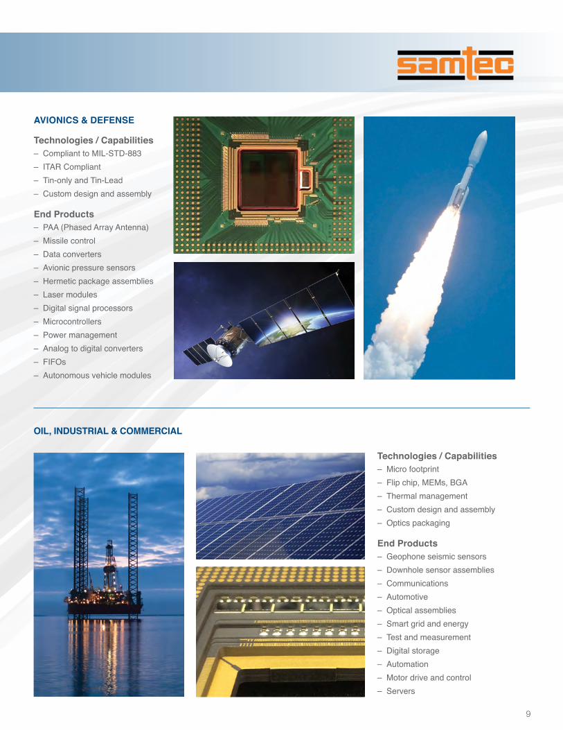
AVIONICS & DEFENSE
Technologies / Capabilities – Compliant to MIL-STD-883 – ITAR Compliant – Tin-only and Tin-Lead – Custom design and assembly
End Products – PAA (Phased Array Antenna) – Missile control – Data converters – Avionic pressure sensors – Hermetic package assemblies – Laser modules – Digital signal processors – Microcontrollers – Power management – Analog to digital converters – FIFOs – Autonomous vehicle modules
Technologies / Capabilities – Micro footprint – Flip chip, MEMs, BGA – Thermal management – Custom design and assembly – Optics packaging
End Products – Geophone seismic sensors – Downhole sensor assemblies – Communications – Automotive – Optical assemblies – Smart grid and energy – Test and measurement – Digital storage – Automation – Motor drive and control – Servers
OIL, INDUSTRIAL & COMMERCIAL

10
DESIGN RULES & GUIDELINES
Samtec Microelectronics Group has an extensive offering of advanced package design and assembly capabilities as well as the ability to assist in choosing the best technology and materials for your specific application.
In addition to substrate and package design, flip chip, die attach, wirebond and sealing, our capabilities also include thermal management, wafer dicing, lid attach and marking.
The following dimensions are designed to help release product to manufacturing as quickly as possible. Please contact Samtec Microelectronics Group at [email protected] if you have tighter requirements.
ADVANCED DESIGN + ASSEMBLY CAPABILITIES
Flip Chip
PACKAGE SIZESmallest size (approx.): 10 mm x 10 mmLargest size (approx.): 63 mm x 63 mm
SOLDER BALL MATERIAL TYPEEutectic Pb:Sn = 37:63
Pb-Free
SUBSTRATE BGA SOLDER BALL SIZESmallest (approx.): 0.018" diameterLargest (approx.): 0.025" diameter
FLUXTacFlux–025 & WS–609
Other no-clean flux-types, water soluble flux-types
SUBSTRATE BGA PAD PITCHClosest pitch (approx.):
0,80 mm x 0,80 mm
Furthest pitch: no constraint
Any configuration of the pad layout is acceptable
Basic guidelines for laying out flip chip substrates including pad design rules, package sizes, solder ball specs, flux, pad pitch and layout, and general structure:
LAYER THICKNESS (TYPICAL)
Location Standard (µm) Custom (µm)
Core Substrate 800 400*
Core Cu 25 21
Build Up Cu 14.5 2
Insulation Layer 33 12
Solder Resist Layer 21 18
Nickel Plating 3 ~ 7
Gold Plating 0.03 ~ 0.12
No. of Build Up Layers: 1, 2, 3, 4 per side; No. of Core Layers: 2, 4*Coreless also available
SPECIFICATIONS (TYPICAL)
Item Standard (µm) Custom (µm)
A Flip Chip Pad Dia. (Solder Resist Opening) 100 75
B Flip Chip Pad Metal Land Diameter 145 100
C Flip Chip Pad Pitch 225 130
D Solder Bump Height 32 +/- 5
Cu Plating Ni Plating Au Plating Solder Bump(Pb:Sn = 37:63)
Cu Plating Ni Plating Au Plating PTH
Solder Resist
2nd Build Up
1st Build Up
Core Substrate (BT Resin)
1st Build Up
2nd Build UpSolder Resist
[FRONT]
[BACK]
TYPICAL SUBSTRATE STRUCTURE
D
C
B
A Solder Bump
Solder Resist
Filled Via
FLIP CHIP PAD DESIGN RULE

11
A
B
C
TOP DOWN
DIE ATTACH REQUIREMENTS
Description Organic (min)Inches (µm)
Ceramic (min) Inches (µm)
Minimum Die Size 0.010" (250) 0.010" (250)
A Overlap of Die Attach Ground Plane to Die Edge 0.020" (500) 0.020" (500)
B Space Between Die Attach Ground Plane to Wirebond Pad
0.020" (500) 0.020" (500)
C Space Between Fiducial Edge to Die Attach Ground Plane Edge
0.010" (250) 0.006" (150)
Die Attach
– Maximum length to width ratio for components: 5:1
– Saw kerfs must be at least 25μm and into the dicing tape (through the entire wafer thickness)
– Die attach materials can be non-conductive, conductive, die-attach-films (DAF) and solder preforms; other processes can be discussed per customer requirements
– Minimum distance between surrounding square of fiducial and neighboring objects must be 0,048 mm
– Gray level contrast between background and fiducial must be a minimum of 100 gray levels out of 256
– Background of fiducial must not have a structure & background must be single-colored gray level
– Maximum die size for dipping: 50 mm x 50 mm – No waffle-pack handling for die < 1 mm2
Plating and layout requirements for substrate pad design as well as wire parameters: – Wedge Bond: ENIG plating is acceptable; typical wire types are Al,
Au and Pt – Ball Bond: ENEPIG plating is recommended; typical wire types are
Au and CuProcesses that use Au ball bond, require Gold plate per MIL-G–45204, Type III, Grade A, Class 1: – 99.9% purity
minimum – < 90 Knoop
hardness – 50μ" thick,
minimum
WirebondWIREBOND DESIGN RULES
Rule Description Organic (min)Inches (µm)
Ceramic (min) Inches (µm)
A Wirebond Pad 0.004" (100) 0.003" (75)
B Wirebond Pad Pitch 0.008" (200) 0.006" (150)
C Overlap of Wirebond Lead Edge to Via 0.008" (200) 0.007" (175)
D Space Solder Mask to Wirebond Lead Edge 0.004" (100) -
E Overlap of Wirebond Lead Edge to Solder Mask 0.008" (200) -
F Space of Die Edge to Wirebond Lead Edge*
0.015" (375) or 2x Die Thickness (whichever is greater)
G Maximum Wire Length 0.250" (6350)
H Maximum Wire Height 0.100" (2540)
*Assumes no ground plane for die attach
SUBSTRATE
DIE
H
G
F
E
D
B
A
C
SIDE PROFILE
SUBSTRATE
DIE
H
G
F
E
D
B
A
C
TOP DOWN
Dam & Encapsulation
– Maximum encapsulation thickness (board surface to top of encapsulation): 0.024" (600)
– Automated dispense tool heated work area: 12" x 16" – Total work area: 20" x 30" – Machine positioning accuracy
and repeatability: +/- 0.001"
SUBSTRATE
DIEE
DC
BA
TOP DOWN
PACKAGE ENCAPSULATION RULES
Rule Description Organic (min)Inches (µm)
A Dam Width 0.012" (300)
B Space of Dam to Wirebond Lead Edge 0.012" (300)
C Space of Fiducial to Dam* 0.007" (175)
D Overlap of Encapsulation to Top of Wirebond Loop 0.007" (175)
E Height of Encapsulation** = A / 2
*Must be outside encapsulated region**Board surface to top of encapsulation
SUBSTRATE
DIEE
DC
BA
SIDE PROFILE

IC-TO-BOARD
SAMTEC USAP.O. Box 1147 • New Albany, IN 47151-1147 USA
+1-800-SAMTEC-9 (USA & Canada) • Tel: +1-812-944-6733 • Fax: +1-812-948-5047 • Email: [email protected]
SAMTEC NORTHERN CALIFORNIA2323 Owen St., Ste 120 • Santa Clara, CA 95054
+1-800-726-8329 (USA & Canada) • Tel: +1-812-944-6733 • Fax: +1-408-217-5171 • Email: [email protected]
SAMTEC SOUTHERN CALIFORNIA5410 Trabuco Road • Suite 120 • Irvine, CA 92620
Tel: +1-800-726-8329 • Email: [email protected] SOUTH AMERICA
Rua Alagoas Nr 1460 • Sala 805 • Bairro Savassi • Belo Horizonte - Minas Gerais 30130-160 • BrazilTel: +55 31 3786 3227 • Fax: +55 31 3786 3229 • Email: [email protected]
SAMTEC UNITED KINGDOM11 Mollins Court • Westfield, Cumbernauld • Scotland G68 9HP
Tel: +44 01236 739292 • Fax: +44 01236 727113 • Email: [email protected]
SAMTEC GERMANYStreiflacher Str. 7 • 82110 Germering • Germany • +0800 SAMTEC9 (+0800 / 72 68 329) Germany only
Tel: +49 (0) 89 / 89460-0 • Fax: +49 (0) 89 / 89460-299 • Email: [email protected]
SAMTEC FRANCEVal d’ Europe Park • 11, rue du Courtalin - Bâtiment B • 77700 Magny le Hongre • France
Tel: +33 1 60 95 06 60 • Fax: +33 1 60 95 06 61 • Email: [email protected]
SAMTEC ITALYVia Colleoni 25 • Centro Direzionale Colleoni • Palazzo Pegaso Ingresso 3 • 20864 Agrate Brianza-Monza Brianza (MB) • Italy
Tel: +39 039 6890337 • Fax: +39 039 6890315 • Email: [email protected]
SAMTEC NORDIC/BALTICSolkraftsvägen 25 • 13570 Stockholm • Sweden
Tel: +46 8 4477280 • Fax: +46 8 7420413 • Email: [email protected]
SAMTEC BENELUX11 Mollins Court • Westfield, Cumbernauld • Scotland G68 9HP
Tel: +44 01236 739292 • Fax: +44 01236 727113 • Email: [email protected]
SAMTEC ISRAEL21 Bar-Kochva St. • Concord Tower • B'nei Brak, Israel 51260
Tel: +972 3 7526600 • Fax: +972 3 7526690 • Email: [email protected]
SAMTEC INDIA #11, 2nd Floor, Chetana, Dattatreya Road • Basavanagudi • Bangalore • 560 004 India
Tel: +91 80 3272 1612 • Fax: +91 80 2662 0967 • Email: [email protected]
SAMTEC ANZ2A San Antonio Court • Mentone 3194 • Victoria, Australia
Tel: +613 9580 0683 • Fax: +613 9580 0684 • Email: [email protected]
SAMTEC SINGAPORE1 Kallang Sector #05-01/02 • Kolam Ayer Industrial Park • Singapore 349276Tel: +65 6745 5955 • Fax: +65 6841 1502 • Email: [email protected]
SAMTEC JAPANNisso No. 16 Bldg. • 3-8-8, Shinyokohama, Kohoku-ku • Yokohama-shi, Kanagawa 222-0033 Japan
Tel: +81 45 475 1385 • Fax: +81 45 475 1340 • Email: [email protected]
SAMTEC SHANGHAIUnit 601, Qilai Building • No 889 Yishan Road • Shanghai, China 200233
Tel: +86 21 6083 3766 • Fax: +86 21 5423 4575 • Email: [email protected]
SAMTEC SHENZHENRm 906B 9/F New World Center Tower • Yi Tian Road, Fu Tian District • Shenzhen, China 518026
Tel: +86 755 83776780 • Fax: +86 755 83776767 • Email: [email protected]
SAMTEC TAIWAN10F, No. 182, Sec. 2 • Dunhua S. Rd. • Da-an District • Taipei City 10669 • Taiwan (R.O.C.)
Tel: 00801 14 9916 (Taiwan only) • Tel: +886 2 2735 6109 • Fax: +886 2 2735 5036 • Email: [email protected]
SAMTEC HONG KONGRoom 18, 13/F, Shatin Galleria • 18-24 Shan Mei Street • Fo Tan, Shatin, Hong Kong
Tel: +852 26904858 • Fax: +852 26904842 • Email: [email protected]
SAMTEC KOREARM#758, Sungwoo Starwoos Officetel Gumi-dong • Seongnam Si, Bundang-gu, Gyeonggi-Do • 463-860 South Korea
Tel: +82 31 717 5685 • Fax: +82 31 717 5681 • Email: [email protected]
SAMTEC ONLINEwww.samtec.com
ISO-9001 and/or TS 16949 Certified
141125


![Area Array Probe Card Interposer - SWTest.org · 2017. 3. 26. · HP54120B Cobra Probe 500 Ohm Picoprobe. 6/4/01 IBM RESEARCH Page [17] TDT Results 500 pS/Div 500 pS/Div TDT of Interposer](https://static.documents.pub/doc/80x56/6070dcd206e5c468b903d38e/area-array-probe-card-interposer-2017-3-26-hp54120b-cobra-probe-500-ohm-picoprobe.jpg)


