24
PWM-FF IC ICE2AS01/S01G ICE2BS01/S01G Off-Line SMPS Current Mode Controller Never stop thinking. Power Management & Supply Datasheet, Version 2.1, 30 Jun 2006

PWM-FF IC
ICE2AS01/S01GICE2BS01/S01GOff-Line SMPS Current Mode Control ler
N e v e r s t o p t h i n k i n g .
P o w e r M a n a g e m e n t & S u p p l y
Datasheet, Version 2.1, 30 Jun 2006
Edition 2006-06-30Published by Infineon Technologies AG,St.-Martin-Strasse 53,D-81541 München© Infineon Technologies AG 1999.All Rights Reserved.
Attention please!The information herein is given to describe certain components and shall not be considered as warranted charac-teristics.Terms of delivery and rights to technical change reserved.We hereby disclaim any and all warranties, including but not limited to warranties of non-infringement, regarding circuits, descriptions and charts stated herein.Infineon Technologies is an approved CECC manufacturer.
InformationFor further information on technology, delivery terms and conditions and prices please contact your nearest Infi-neon Technologies Office in Germany or our Infineon Technologies Representatives worldwide (see address list).
WarningsDue to technical requirements components may contain dangerous substances. For information on the types in question please contact your nearest Infineon Technologies Office.Infineon Technologies Components may only be used in life-support devices or systems with the express written approval of Infineon Technologies, if a failure of such components can reasonably be expected to cause the failure of that life-support device or system, or to affect the safety or effectiveness of that device or system. Life support devices or systems are intended to be implanted in the human body, or to support and/or maintain and sustain and/or protect human life. If they fail, it is reasonable to assume that the health of the user or other persons may be endangered.
For questions on technology, delivery and prices please contact the Infineon Technologies Offices in Germany orthe Infineon Technologies Companies and Representatives worldwide: see our webpage at http://www.infineon.com
CoolMOS™, CoolSET™ are trademarks of Infineon Technologies AG.
ICE2AS01/S01GICE2BS01/S01G
Revision History: 2006-06-30 DatasheetPrevious Version: V2.0Page Subjects (major changes since last revision)3,5,15,23 update to PB-free package
We Listen to Your CommentsAny information within this document that you feel is wrong, unclear or missing at all?Your feedback will help us to continuously improve the quality of this document.Please send your proposal (including a reference to this document) to:[email protected]

Datasheet 3 30 Jun 2006
Type Frequency Package
ICE2AS01 100kHz PG-DIP-8
ICE2AS01G 100kHz PG-DSO-8
ICE2BS01 67kHz PG-DIP-8
ICE2BS01G 67kHz PG-DSO-8
ICE2AS01/S01GICE2BS01/S01G
P-DIP-8-4PG-DIP-8
P-DSO-8-3PG-DSO-8
CSoft Start
CVCC
RStart-up
VCC
-
ConverterDC Output
+
ICE2AS01(G) / ICE2BS01(G)
Snubber
PowerManagement
Protection Unit
Soft-Start Control PWM ControllerCurrent Mode
FB
85 ... 270 VAC
Feedback
Feedback
Typical Application
Low PowerStandBy
Precise Low TolerancePeak Current Limitation
RSense
Isense
GND
SoftS Gate
Off-Line SMPS Current Mode Controller
Product Highlights
• Enhanced Protection Functions all with Auto Restart
• Lowest Standby Power Dissipation• Very Accurate Current Limiting• PB-free Plating and RoHS compliant
Features• Only few external Components required• Input Undervoltage Lockout• 67kHz/100kHz fixed Switching Frequency• Max Duty Cycle 72% • Low Power Standby Mode to support
“Blue Angel” Norm• Latched Thermal Shut Down• Overload and Open Loop Protection• Overvoltage Protection during Auto Restart• Adjustable Peak Current Limitation via
External Resistor• Overall Tolerance of Current Limiting < ±5%• Internal Leading Edge Blanking• Soft Start • Soft gate driving for Low EMI
DescriptionThis stand alone controller provides several specialenhancements to satisfy the needs for low power standbyand protection features. In standby mode frequencyreduction is used to lower the power consumption andprovide a stable output voltage in this mode. The frequencyreduction is limited to 20kHz / 21.5 kHz (typ.) to avoidaudible noise. In case of failure modes like open loop,overvoltage or overload due to short circuit the deviceswitches in Auto Restart Mode which is controlled by theinternal protection unit. By means of the internal precisepeak current limitation the dimension of the transformer andthe secondary diode can be lower which leads to more costefficiency.

ICE2AS01/S01GICE2BS01/S01G
Table of Contents Page
Datasheet 4 30 Jun 2006Preliminary Data
1 Pin Configuration and Functionality . . . . . . . . . . . . . . . . . . . . . . . . . . . . .51.1 Pin Configuration . . . . . . . . . . . . . . . . . . . . . . . . . . . . . . . . . . . . . . . . . . . . . .51.2 Pin Functionality . . . . . . . . . . . . . . . . . . . . . . . . . . . . . . . . . . . . . . . . . . . . . .5
2 Representative Blockdiagram . . . . . . . . . . . . . . . . . . . . . . . . . . . . . . . . . .6
3 Functional Description . . . . . . . . . . . . . . . . . . . . . . . . . . . . . . . . . . . . . . . .73.1 Power Management . . . . . . . . . . . . . . . . . . . . . . . . . . . . . . . . . . . . . . . . . . . .73.2 Improved Current Mode . . . . . . . . . . . . . . . . . . . . . . . . . . . . . . . . . . . . . . . . .73.2.1 PWM-OP . . . . . . . . . . . . . . . . . . . . . . . . . . . . . . . . . . . . . . . . . . . . . . . . . .83.2.2 PWM-Comparator . . . . . . . . . . . . . . . . . . . . . . . . . . . . . . . . . . . . . . . . . . .83.3 Soft-Start . . . . . . . . . . . . . . . . . . . . . . . . . . . . . . . . . . . . . . . . . . . . . . . . . . . .93.4 Oscillator and Frequency Reduction . . . . . . . . . . . . . . . . . . . . . . . . . . . . . .103.4.1 Oscillator . . . . . . . . . . . . . . . . . . . . . . . . . . . . . . . . . . . . . . . . . . . . . . . . .103.4.2 Frequency Reduction . . . . . . . . . . . . . . . . . . . . . . . . . . . . . . . . . . . . . . . .103.5 Current Limiting . . . . . . . . . . . . . . . . . . . . . . . . . . . . . . . . . . . . . . . . . . . . . .103.5.1 Leading Edge Blanking . . . . . . . . . . . . . . . . . . . . . . . . . . . . . . . . . . . . . .103.5.2 Propagation Delay Compensation . . . . . . . . . . . . . . . . . . . . . . . . . . . . . .113.6 PWM-Latch . . . . . . . . . . . . . . . . . . . . . . . . . . . . . . . . . . . . . . . . . . . . . . . . .113.7 Driver . . . . . . . . . . . . . . . . . . . . . . . . . . . . . . . . . . . . . . . . . . . . . . . . . . . . . .113.8 Protection Unit (Auto Restart Mode) . . . . . . . . . . . . . . . . . . . . . . . . . . . . . .123.8.1 Overload & Open loop with normal load . . . . . . . . . . . . . . . . . . . . . . . . .123.8.2 Overvoltage due to open loop with no load . . . . . . . . . . . . . . . . . . . . . . .133.8.3 Thermal Shut Down . . . . . . . . . . . . . . . . . . . . . . . . . . . . . . . . . . . . . . . . .14
4 Electrical Characteristics . . . . . . . . . . . . . . . . . . . . . . . . . . . . . . . . . . . . .154.1 Absolute Maximum Ratings . . . . . . . . . . . . . . . . . . . . . . . . . . . . . . . . . . . . .154.2 Operating Range . . . . . . . . . . . . . . . . . . . . . . . . . . . . . . . . . . . . . . . . . . . . .154.3 Characteristics . . . . . . . . . . . . . . . . . . . . . . . . . . . . . . . . . . . . . . . . . . . . . . .164.3.1 Supply Section . . . . . . . . . . . . . . . . . . . . . . . . . . . . . . . . . . . . . . . . . . . . .164.3.2 Internal Voltage Reference . . . . . . . . . . . . . . . . . . . . . . . . . . . . . . . . . . .164.3.3 Control Section . . . . . . . . . . . . . . . . . . . . . . . . . . . . . . . . . . . . . . . . . . . .164.3.4 Protection Unit . . . . . . . . . . . . . . . . . . . . . . . . . . . . . . . . . . . . . . . . . . . . .174.3.5 Current Limiting . . . . . . . . . . . . . . . . . . . . . . . . . . . . . . . . . . . . . . . . . . . .174.3.6 Driver Section . . . . . . . . . . . . . . . . . . . . . . . . . . . . . . . . . . . . . . . . . . . . .17
5 Typical Performance Characteristics . . . . . . . . . . . . . . . . . . . . . . . . . . .19
6 Outline Dimension . . . . . . . . . . . . . . . . . . . . . . . . . . . . . . . . . . . . . . . . . . .23

Datasheet 5 30 Jun 2006Preliminary Data
ICE2AS01/S01GICE2BS01/S01G
1
Figure 1 Pin Configuration (top view)
1.2 Pin Functionality
SoftS (Soft Start & Auto Restart Control)This pin combines the function of Soft Start in case ofStart Up and Auto Restart Mode and the controlling ofthe Auto Restart Mode in case of an error detection.
FB (Feedback)The information about the regulation is provided by theFB Pin to the internal Protection Unit and to the internalPWM-Comparator to control the duty cycle.
Isense (Current Sense)The Current Sense pin senses the voltage developedon the series resistor inserted in the source of theexternal Power Switch. When Isense reaches theinternal threshold of the Current Limit Comparator, theDriver output is disabled. By this mean the OverCurrent Detection is realized.Furthermore the current information is provided for thePWM-Comparator to realize the Current Mode.
Gate (Driver Output)The current and slew rate capability of this pin aresuited to drive Power MOSFETs.
VCC (Power supply)This pin is the positive supply of the IC. The operatingrange is between 8.5V and 21V.To provide overvoltage protection the driver getsdisabled when the voltage becomes higher than 16.5Vduring Start up Phase.
GND (Ground)This pin is the ground of the primary side of the SMPS.
1.1 Pin Configuration
Pin Symbol Function
1 N.C. Not connected
2 SoftS Soft Start & Auto Restart Control
3 FB Regulation Feedback
4 Isense Controller Current Sense Input
5 Gate Driver Output
6 VCC Controller Supply Voltage
7 GND Controller Ground
8 N.C. Not connected
1
6
7
8
4
3
2
5
GNDSoftS
FB
Isense
N.C.
VCC
N.C.
Gate
Package PG-DIP-8G-Package PG-DSO-8
1 Pin Configuration and Functionality

ICE2AS01/S01GICE2BS01/S01G
Representative Blockdiagram
Datasheet 6 30 Jun 2006
2 Representative Blockdiagram
Figure 2
Ther
mal
Shut
down
T j >14
0°C
Inte
rnal
Bias
Volta
geR
efer
ence
6.5V
4.8V
Lead
ing
Edge
Blan
king
200n
s
Unde
rvol
tage
Lock
out
Osc
illato
rDu
ty C
ycle
max
Curre
nt-L
imit
Com
para
tor
x3.6
5Soft-
Star
tCo
mpa
rato
r
Curr
ent L
imiti
ngPW
M O
P
Impr
oved
Cur
rent
Mod
e
Soft
Star
t
13.5
V
8.5V
6.5V
C2
C1
16.5
V
4.0V
R FB
6.5V
Prot
ectio
n Un
it
Pow
er-D
own
Rese
t
Powe
r-Up
Res
et
Pow
er M
anag
emen
t
C Soft-
Star
t
CVC
C
R Star
t-up
85 ..
. 270
VAC
C Line
VCC
GND
+ -
Con
verte
rDC
Out
put
V OUT
ICE2
AS01
(G) /
ICE2
BS01
(G)
Opt
ocou
pler
Snub
ber
Spike
Blan
king
5µs
PWM
Com
para
tor
RSQ Q
Erro
r-Lat
ch
C4
5.3V
C3
4.8V
R Soft-
Star
t
Gat
eDr
iver
G3
G2
G1
G4
SoftS
5.3V
T1
V csth
Prop
agat
ion-
Dela
yCo
mpe
nsat
ion
RS
QQPW
M-L
atch
0.72
Cloc
k
U FB
f osc
f norm
f stan
dby
Stan
dby
Unit
FB
4.0V
RSe
nse
Gat
e
Isen
se0.
8V
C50.
3V
5.6V
10kΩ
D1
Freq
uenc
y in
Nor
mal
Mod
e f no
rm:
ICE2
BS01
(G)I
CE2A
S01(
G)
67kH
z10
0kHz
Freq
uenc
y in
Sta
ndby
Mod
e f st
andb
y:20
kHz
21.5
kHz
Datasheet 7 30 Jun 2006Preliminary Data
ICE2AS01/S01GICE2BS01/S01G
Functional Description
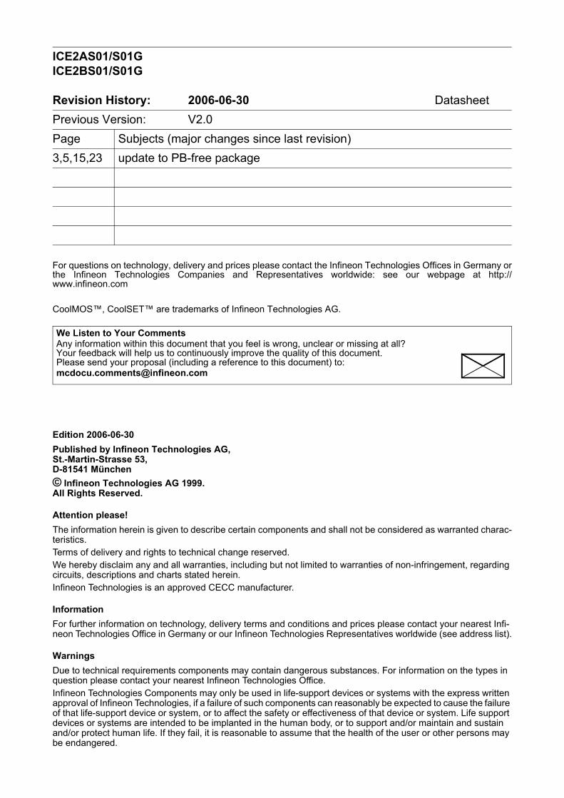
3 Functional Description3.1 Power Management
Figure 3 Power Management
The Undervoltage Lockout monitors the externalsupply voltage VVCC. In case the IC is inactive thecurrent consumption is max. 55µA. When the SMPS isplugged to the main line the current through RStart-upcharges the external Capacitor CVCC. When VVCCexceeds the on-threshold VCCon=13.5V the internal biascircuit and the voltage reference are switched on. Afterit the internal bandgap generates a reference voltageVREF=6.5V to supply the internal circuits. To avoiduncontrolled ringing at switch-on a hysteresis isimplemented which means that switch-off is only afteractive mode when Vcc falls below 8.5V.In case of switch-on a Power Up Reset is done byreseting the internal error-latch in the protection unit.When VVCC falls below the off-threshold VCCoff=8.5V theinternal reference is switched off and the Power Downreset let T1 discharging the soft-start capacitor CSoft-Startat pin SoftS. Thus it is ensured that at every switch-onthe voltage ramp at pin SoftS starts at zero.
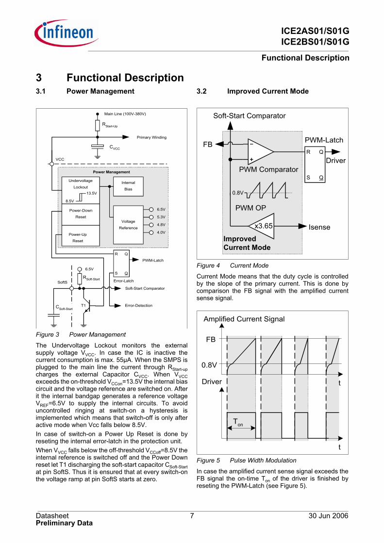
3.2 Improved Current Mode
Figure 4 Current Mode
Current Mode means that the duty cycle is controlledby the slope of the primary current. This is done bycomparison the FB signal with the amplified currentsense signal.
Figure 5 Pulse Width Modulation
In case the amplified current sense signal exceeds theFB signal the on-time Ton of the driver is finished byreseting the PWM-Latch (see Figure 5).
Internal
Bias
Voltage
Reference
6.5V
4.8V
Undervoltage
Lockout13.5V
8.5V
Power-Down
Reset
Power-Up
Reset
Power Management
5.3V
4.0V
T1
PWM-Latch
R
S
Q
Q
Error-LatchSoftS
6.5V
Error-Detection
VCC
Main Line (100V-380V)
Primary Winding
Soft-Start Comparator
CVCC
RSoft-Start
RStart-Up
CSoft-Start
x3.65
PWM OP
ImprovedCurrent Mode
0.8V
PWM Comparator
PWM-Latch
Isense
FBR
S
Q
Q
Driver
Soft-Start Comparator
t
FB
Amplified Current Signal
Ton
t
0.8V
Driver
Datasheet 8 30 Jun 2006Preliminary Data
ICE2AS01/S01GICE2BS01/S01G
Functional Description
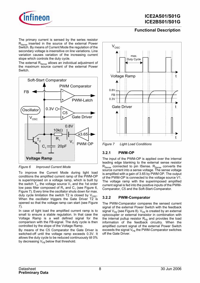
The primary current is sensed by the series resistorRSense inserted in the source of the external PowerSwitch. By means of Current Mode the regulation of thesecondary voltage is insensitive on line variations. Linevariation causes variation of the increasing currentslope which controls the duty cycle.The external RSense allows an individual adjustment ofthe maximum source current of the external PowerSwitch.
Figure 6 Improved Current Mode
To improve the Current Mode during light loadconditions the amplified current ramp of the PWM-OPis superimposed on a voltage ramp, which is built bythe switch T2, the voltage source V1 and the 1st orderlow pass filter composed of R1 and C1 (see Figure 6,Figure 7). Every time the oscillator shuts down for max.duty cycle limitation the switch T2 is closed by VOSC.When the oscillator triggers the Gate Driver T2 isopened so that the voltage ramp can start (see Figure7).In case of light load the amplified current ramp is tosmall to ensure a stable regulation. In that case theVoltage Ramp is a well defined signal for thecomparison with the FB-signal. The duty cycle is thencontrolled by the slope of the Voltage Ramp.By means of the C5 Comparator the Gate Driver isswitched-off until the voltage ramp exceeds 0.3V. Itallows the duty cycle to be reduced continuously till 0%by decreasing VFB below that threshold.
Figure 7 Light Load Conditions
3.2.1 PWM-OPThe input of the PWM-OP is applied over the internalleading edge blanking to the external sense resistorRSense connected to pin ISense. RSense converts thesource current into a sense voltage. The sense voltageis amplified with a gain of 3.65 by PWM OP. The outputof the PWM-OP is connected to the voltage source V1.The voltage ramp with the superimposed amplifiedcurrent signal is fed into the positive inputs of the PWM-Comparator, C5 and the Soft-Start-Comparator.
3.2.2 PWM-ComparatorThe PWM-Comparator compares the sensed currentsignal of the external Power Switch with the feedbacksignal VFB (see Figure 8). VFB is created by an externaloptocoupler or external transistor in combination withthe internal pullup resistor RFB and provides the loadinformation of the feedback circuitry. When theamplified current signal of the external Power Switchexceeds the signal VFB the PWM-Comparator switchesoff the Gate Driver.
x3.65
PWM OP
0.8V10kΩ
Oscillator
PWM Comparator
20pF
T2R1
C1
FB
PWM-Latch
V1
C50.3V
Gate Driver
Voltage Ramp
VOSC
Soft-Start Comparatort
t
VOSC
0.8V
FB
Gate Driver
Voltage Ramp
t
max.Duty Cycle
0.3V
Datasheet 9 30 Jun 2006Preliminary Data
ICE2AS01/S01GICE2BS01/S01G
Functional Description
Figure 8 PWM Controlling
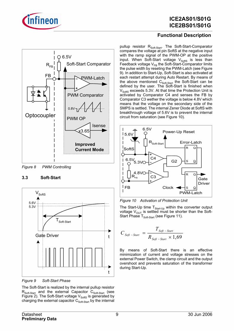
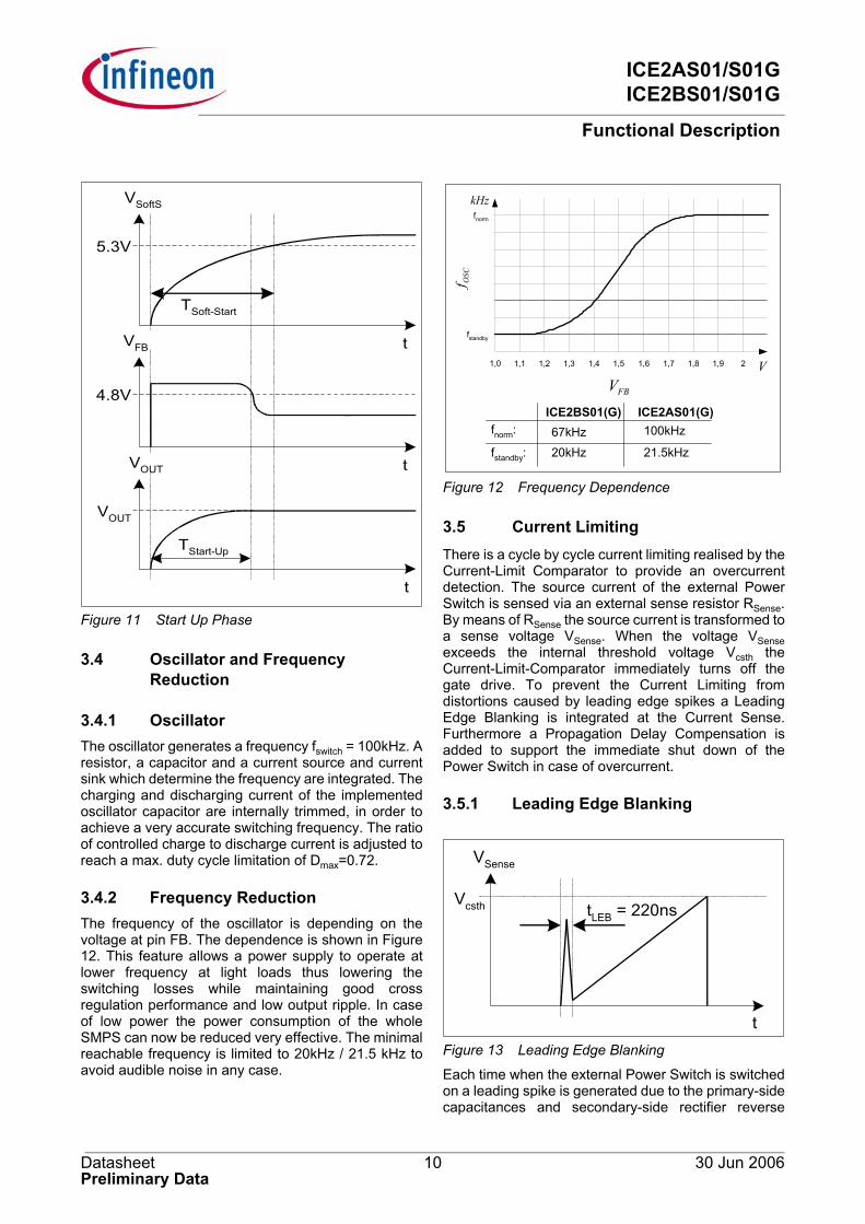
3.3 Soft-Start
Figure 9 Soft-Start Phase
The Soft-Start is realized by the internal pullup resistorRSoft-Start and the external Capacitor CSoft-Start (seeFigure 2). The Soft-Start voltage VSoftS is generated bycharging the external capacitor CSoft-Start by the internal
pullup resistor RSoft-Start. The Soft-Start-Comparatorcompares the voltage at pin SoftS at the negative inputwith the ramp signal of the PWM-OP at the positiveinput. When Soft-Start voltage VSoftS is less thanFeedback voltage VFB the Soft-Start-Comparator limitsthe pulse width by reseting the PWM-Latch (see Figure9). In addition to Start-Up, Soft-Start is also activated ateach restart attempt during Auto Restart. By means ofthe above mentioned CSoft-Start the Soft-Start can bedefined by the user. The Soft-Start is finished whenVSoftS exceeds 5.3V. At that time the Protection Unit isactivated by Comparator C4 and senses the FB byComparator C3 wether the voltage is below 4.8V whichmeans that the voltage on the secondary side of theSMPS is settled. The internal Zener Diode at SoftS withbreakthrough voltage of 5.6V is to prevent the internalcircuit from saturation (see Figure 10).
Figure 10 Activation of Protection Unit
The Start-Up time TStart-Up within the converter outputvoltage VOUT is settled must be shorter than the Soft-Start Phase TSoft-Start (see Figure 11).
By means of Soft-Start there is an effectiveminimization of current and voltage stresses on theexternal Power Switch, the clamp circuit and the outputovershoot and prevents saturation of the transformerduring Start-Up.
x3.65
PWM OP
ImprovedCurrent Mode
PWM Comparator
Isense
Soft-Start Comparator6.5V
PWM-Latch
0.8V
FB
Optocoupler
RFB
t
5.3V
VSoftS
Gate Driver
t
TSoft-Start
5.6V
6.5V
RFB
6.5V
Power-Up Reset
C45.3V
C34.8V
RSoft-Start
FB
R
S
Q
Q
Error-Latch
R
S
Q
Q
PWM-Latch
G2
Clock
GateDriver
5.6V
SoftS
69,1×=
−
−−
StartSoft
StartSoftStartSoft R
TC
Datasheet 10 30 Jun 2006Preliminary Data
ICE2AS01/S01GICE2BS01/S01G
Functional Description
Figure 11 Start Up Phase
3.4 Oscillator and Frequency Reduction
3.4.1 OscillatorThe oscillator generates a frequency fswitch = 100kHz. Aresistor, a capacitor and a current source and currentsink which determine the frequency are integrated. Thecharging and discharging current of the implementedoscillator capacitor are internally trimmed, in order toachieve a very accurate switching frequency. The ratioof controlled charge to discharge current is adjusted toreach a max. duty cycle limitation of Dmax=0.72.
3.4.2 Frequency ReductionThe frequency of the oscillator is depending on thevoltage at pin FB. The dependence is shown in Figure12. This feature allows a power supply to operate atlower frequency at light loads thus lowering theswitching losses while maintaining good crossregulation performance and low output ripple. In caseof low power the power consumption of the wholeSMPS can now be reduced very effective. The minimalreachable frequency is limited to 20kHz / 21.5 kHz toavoid audible noise in any case.
Figure 12 Frequency Dependence
3.5 Current LimitingThere is a cycle by cycle current limiting realised by theCurrent-Limit Comparator to provide an overcurrentdetection. The source current of the external PowerSwitch is sensed via an external sense resistor RSense.By means of RSense the source current is transformed toa sense voltage VSense. When the voltage VSenseexceeds the internal threshold voltage Vcsth theCurrent-Limit-Comparator immediately turns off thegate drive. To prevent the Current Limiting fromdistortions caused by leading edge spikes a LeadingEdge Blanking is integrated at the Current Sense.Furthermore a Propagation Delay Compensation isadded to support the immediate shut down of thePower Switch in case of overcurrent.
3.5.1 Leading Edge Blanking
Figure 13 Leading Edge Blanking
Each time when the external Power Switch is switchedon a leading spike is generated due to the primary-sidecapacitances and secondary-side rectifier reverse
t
t
VSoftS
t
5.3V
4.8V
TSoft-Start
VOUT
VFB
VOUT
TStart-Up
fstandby
fnorm
1,0 1,1 1,2 1,3 1,4 1,5 1,6 1,7 1,8 1,9 2
FBVV
kHz
OSCf
fnorm:ICE2BS01(G) ICE2AS01(G)67kHz 100kHz
fstandby: 20kHz 21.5kHz
t
VSense
Vcsth tLEB = 220ns
Datasheet 11 30 Jun 2006Preliminary Data
ICE2AS01/S01GICE2BS01/S01G
Functional Description
recovery time. To avoid a premature termination of theswitching pulse this spike is blanked out with a timeconstant of tLEB = 220ns. During that time the output ofthe Current-Limit Comparator cannot switch off thegate drive.
3.5.2 Propagation Delay CompensationIn case of overcurrent detection the shut down of theexternal Power Switch is delayed due to thepropagation delay of the circuit. This delay causes anovershoot of the peak current Ipeak which depends onthe ratio of dI/dt of the peak current (see Figure 14)..
Figure 14 Current Limiting
The overshoot of Signal2 is bigger than of Signal1 dueto the steeper rising waveform.A propagation delay compensation is integrated tobound the overshoot dependent on dI/dt of the risingprimary current. That means the propagation delaytime between exceeding the current sense thresholdVcsth and the switch off of the external Power Switch iscompensated over temperature within a range of atleast.
So current limiting is now capable in a very accurateway (see Figure 16).E.g. Ipeak = 0.5A with RSense = 2. Without propagationdelay compensation the current sense threshold is setto a static voltage level Vcsth=1V. A current ramp of dI/dt = 0.4A/µs, that means dVSense/dt = 0.8V/µs, and apropagation delay time of i.e. tPropagation Delay =180nsleads then to an Ipeak overshoot of 14.4%. By means ofpropagation delay compensation the overshoot is onlyabout 2% (see Figure 15). The propagation delay compensation is done bymeans of a dynamic threshold voltage Vcsth (see Figure15). In case of a steeper slope the switch off of thedriver is earlier to compensate the delay.
Figure 15 Dynamic Voltage Threshold Vcsth
Figure 16 Overcurrent Shutdown
3.6 PWM-LatchThe oscillator clock output applies a set pulse to thePWM-Latch when initiating the external Power Switchconduction. After setting the PWM-Latch can be resetby the PWM-OP, the Soft-Start-Comparator, theCurrent-Limit-Comparator, Comparator C3 or theError-Latch of the Protection Unit. In case of resetingthe driver is shut down immediately.
3.7 DriverThe driver is a fast totem pole gate drive, which isdesigned to avoid cross conduction currents and whichis equipped with a Zener diode Z1 (see Figure 17) inorder to improve the control of the gate attached power
t
ISense
ILimit
tPropagation Delay
IOvershoot1
Ipeak1
Signal1Signal2
IOvershoot2Ipeak2
dtdV
dtdI
R SensepeakSense 10 ≤×≤
t
Vcsth
VOSC
Signal1 Signal2
VSense Propagation Delay
max. Duty Cycle
off time
t
0,9
0,95
1
1,05
1,1
1,15
1,2
1,25
1,3
0 0,2 0,4 0,6 0,8 1 1,2 1,4 1,6 1,8 2
with compensation without compensation
dtdVSense s
Vµ
Sense
V
V

Datasheet 12 30 Jun 2006Preliminary Data
ICE2AS01/S01GICE2BS01/S01G
Functional Description
transistors as well as to protect them againstundesirable gate overvoltages.
Figure 17 Gate Driver
At voltages below the undervoltage lockout thresholdVVCCoff the gate drive is active low.The driver-stage is optimized to minimize EMI and toprovide high circuit efficiency. This is done by reducingthe switch on slope when reaching the external PowerSwitch threshold. This is achieved by a slope control ofthe rising edge at the driver’s output (see Figure 18).
Figure 18 Gate Rising Slope
Thus the leading switch on spike is minimized. Whenthe external Power Switch is switched off, the fallingshape of the driver is slowed down when reaching 2Vto prevent an overshoot below ground. Furthermore thedriver circuit is designed to eliminate cross conductionof the output stage.
3.8 Protection Unit (Auto Restart Mode)An overload, open loop and overvoltage detection isintegrated within the Protection Unit. These three
failure modes are latched by an Error-Latch. Additionalthermal shutdown is latched by the Error-Latch. In caseof those failure modes the Error-Latch is set after ablanking time of 5µs and the external Power Switch isshut down. That blanking prevents the Error-Latch fromdistortions caused by spikes during operation mode.
3.8.1 Overload & Open loop with normalload
Figure 19 Auto Restart Mode
Figure 19 shows the Auto Restart Mode in case ofoverload or open loop with normal load. The detectionof open loop or overload is provided by the ComparatorC3, C4 and the AND-gate G2 (see Figure20).
Z1
VCC
1
PWM-Latch
Gate
t
VGate
5V
CLoad = 1nF
ca. t = 130ns
Overload & Open loop/normal load
FB
t
4.8V
5.3V
SoftS
5µs Blanking
FailureDetection
Soft-Start Phase
VCC
13.5V
8.5V
t
Driver
t
TRestart
TBurst1t

Datasheet 13 30 Jun 2006Preliminary Data
ICE2AS01/S01GICE2BS01/S01G
Functional Description
Figure 20 FB-Detection
The detection is activated by C4 when the voltage atpin SoftS exceeds 5.3V. Till this time the IC operates inthe Soft-Start Phase. After this phase the comparatorC3 can set the Error-Latch in case of open loop oroverload which leads the feedback voltage VFB toexceed the threshold of 4.8V. After latching VCCdecreases till 8.5V and inactivates the IC. At this timethe external Soft-Start capacitor is discharged by theinternal transistor T1 due to Power Down Reset. Whenthe IC is inactive VCC increases till VCCon = 13.5V bycharging the Capacitor CVCC by means of the Start-UpResistor RStart-Up. Then the Error-Latch is reset byPower Up Reset and the external Soft-Start capacitorCSoft-Start is charged by the internal pullup resistor RSoft-
Start. During the Soft-Start Phase which ends when thevoltage at pin SoftS exceeds 5.3V the detection ofoverload and open loop by C3 and G2 is inactive. In thisway the Start Up Phase is not detected as an overload.But the Soft-Start Phase must be finished within theStart Up Phase to force the voltage at pin FB below thefailure detection threshold of 4.8V.
3.8.2 Overvoltage due to open loop withno load
Figure 21 Auto Restart Mode
Figure 21 shows the Auto Restart Mode for open loopand no load condition. In case of this failure mode theconverter output voltage increases and also VCC. Anadditional protection by the comparators C1, C2 andthe AND-gate G1 is implemented to consider thisfailure mode (see Figure 22).
RSoft-Start
6.5V
CSoft-StartC4
5.3V
C34.8V
G2T1
Error-Latch
Power Up Reset
RFB
6.5V
FB
SoftS Open loop & no load condition
t
Driver
13.5V16.5V
FB
4.8V
5µs Blanking
FailureDetection
5.3V
SoftS
4.0V OvervoltageDetection Phase
Soft-Start Phase
t
t
TRestart
TBurst2
VCC
8.5V
Overvoltage Detection
t

Datasheet 14 30 Jun 2006Preliminary Data
ICE2AS01/S01GICE2BS01/S01G
Functional Description
Figure 22 Overvoltage Detection
The overvoltage detection is provided by ComparatorC1 only in the first time during the Auto Restart Modetill the Soft-Start voltage exceeds the threshold of theComparator C2 at 4.0V and the voltage at pin FB isabove 4.8V. When VCC exceeds 16.5V during theovervoltage detection phase C1 can set the Error-Latchand the Burst Phase during Auto Restart Mode isfinished earlier. In that case TBurst2 is shorter than TSoft-
Start. By means of C2 the normal operation mode isprevented from overvoltage detection due to varying ofVCC concerning the regulation of the converter output.When the voltage VSoftS is above 4.0V the overvoltagedetection by C1 is deactivated.
3.8.3 Thermal Shut DownThermal Shut Down is latched by the Error-Latch whenjunction temperature Tj of the pwm controller isexceeding an internal threshold of 140°C. In that casethe IC switches in Auto Restart Mode.
Note: All the values which are mentioned in thefunctional description are typical. Please referto Electrical Characteristics for min/max limitvalues.
6.5V
CSoft-Start
VCC
RSoft-Start
C116.5V
C24.0V
T1
SoftS
G1Error Latch
Power Up Reset

ICE2AS01/S01GICE2BS01/S01G
Electrical Characteristics
Datasheet 15 30 Jun 2006
4 Electrical Characteristics
4.1 Absolute Maximum RatingsNote: Absolute maximum ratings are defined as ratings, which when being exceeded may lead to destruction
of the integrated circuit. For the same reason make sure, that any capacitor that will be connected to pin 6(VCC) is discharged before assembling the application circuit.
4.2 Operating RangeNote: Within the operating range the IC operates as described in the functional description.
Parameter Symbol Limit Values Unit Remarks
min. max.
VCC Supply Voltage VCC -0.3 22 V
FB Voltage VFB -0.3 6.5 V
SoftS Voltage VSoftS -0.3 6.5 V
ISense ISense -0.3 3 V
Junction Temperature Tj -40 150 °C Controller & CoolMOS
Storage Temperature TS -50 150 °C
Thermal Resistance Junction-Ambient
RthJA - 90 K/W PG-DIP-8
Thermal Resistance Junction-Ambient
RthJA - 185 K/W PG-DSO-8
ESD Capability1)
1) Equivalent to discharging a 100pF capacitor through a 1.5 kΩ series resistor
VESD - 2 kV Human Body Model
Parameter Symbol Limit Values Unit Remarks
min. max.
VCC Supply Voltage VCC VCCoff 21 V
Junction Temperature of Controller
TJCon -25 130 °C limited due to thermal shut down of controller

ICE2AS01/S01GICE2BS01/S01G
Electrical Characteristics
Datasheet 16 30 Jun 2006
4.3 CharacteristicsNote: The electrical characteristics involve the spread of values guaranteed within the specified supply voltage
and junction temperature range TJ from – 25 °C to 125 °C.Typical values represent the median values,which are related to 25°C. If not otherwise stated, a supply voltage of VCC = 15 V is assumed.
4.3.1 Supply Section
4.3.2 Internal Voltage Reference
4.3.3 Control Section
Parameter Symbol Limit Values Unit Test Condition
min. typ. max.
Start Up Current IVCC1 - 27 55 µA VCC=VCCon -0.1V
Supply Current with Inactive Gate
IVCC2 - 5.3 7 mA VSoftS = 0IFB = 0
Supply Current with Active GateICE2AS01/G
IVCC3 - 6.5 8 mA VSoftS = 5VIFB = 0CGate = 1nF
Supply Current with Active GateICE2BS01/G
IVCC3 - 6 7.5 mA VSoftS = 5VIFB = 0CGate = 1nF
VCC Turn-On ThresholdVCC Turn-Off ThresholdVCC Turn-On/Off Hysteresis
VCConVCCoffVCCHY
13-4.5
13.58.55
14-5.5
VVV
Parameter Symbol Limit Values Unit Test Condition
min. typ. max.
Trimmed Reference Voltage VREF 6.37 6.50 6.63 V measured at pin FB
Parameter Symbol Limit Values Unit Test Condition
min. typ. max.
Oscillator Frequency ICE2AS01/G
fOSC1 93 100 107 kHz VFB = 4V
Oscillator Frequency ICE2BS01/G
fOSC3 62 67 72 kHz VFB = 4V
Reduced Osc. Frequency ICE2AS01/G
fOSC2 - 21.5 - kHz VFB = 1V
Reduced Osc. Frequency ICE2AS01/G
fOSC4 - 20 - kHz VFB = 1V

ICE2AS01/S01GICE2BS01/S01G
Electrical Characteristics
Datasheet 17 30 Jun 2006
4.3.4 Protection Unit
4.3.5 Current Limiting
Frequency Ratio fosc1/fosc2ICE2AS01/G
4.5 4.65 4.9
Frequency Ratio fosc3/fosc4ICE2BS01/G
3.18 3.35 3.53
Max Duty Cycle Dmax 0.67 0.72 0.77
Min Duty Cycle Dmin 0 - - VFB < 0V
PWM-OP Gain AV 3.45 3.65 3.85
Max. Level of Voltage Ramp VMax-Ramp - 0.85 - V
VFB Operating Range Min Level VFBmin 0.3 - - V
VFB Operating Range Max level VFBmax - - 4.6 V
Feedback Resistance RFB 3.0 3.7 4.9 kΩ
Soft-Start Resistance RSoft-Start 42 50 62 kΩ
Parameter Symbol Limit Values Unit Test Condition
min. typ. max.
Over Load & Open Loop Detection Limit
VFB2 4.65 4.8 4.95 V VSoftS > 5.5V
Activation Limit of Overload & Open Loop Detection
VSoftS1 5.15 5.3 5.46 V VFB > 5V
Deactivation Limit of Overvoltage Detection
VSoftS2 3.88 4.0 4.12 V VFB > 5VVCC > 17.5V
Overvoltage Detection Limit VVCC1 16 16.5 17.2 V VSoftS < 3.8VVFB > 5V
Latched Thermal Shutdown TjSD 130 140 150 °C guaranteed by design
Spike Blanking tSpike - 5 - µs
Parameter Symbol Limit Values Unit Test Condition
min. typ. max.
Peak Current Limitation (incl. Propagation Delay Time)(see Figure 7)
Vcsth 0.95 1.00 1.05 V dVsense / dt = 0.6V/µs
Leading Edge Blanking tLEB - 220 - ns
ICE2AS01/S01GICE2BS01/S01G
Electrical Characteristics
Datasheet 18 30 Jun 2006
4.3.6 Driver Section
Parameter Symbol Limit Values Unit Test Condition
min. typ. max.
GATE Low Voltage VGATE - 0.95 1.2 V VVCC = 5 VIGate = 5 mA
- 1.0 1.5 V VVCC = 5 VIGate = 20 mA
- 0.88 - V IGate = 0 A
- 1.6 2.2 V IGate = 50 mA
-0.2 0.2 - V IGate = -50 mA
GATE High Voltage VGATE - 11.5 - V VVCC = 20VCL = 4.7nF
- 10 - V VVCC = 11VCL = 4.7nF
- 7.5 - V VVCC = VVCCoff + 0.2VCL = 4.7nF
GATE Rise Time tr - 160 - ns VGate = 2V...9V1)
CL = 4.7nF
1) Transient reference value
GATE Fall Time tf - 65 - ns VGate = 9V...2V1)
CL = 4.7nF
GATE Current, Peak, Rising Edge
IGATE -0.5 - - A CL = 4.7nF2)
2) Design characteristics (not meant for production testing)
GATE Current, Peak,Falling Edge
IGATE - - 0.7 A CL = 4.7nF2)

Datasheet 19 30 Jun 2006Preliminary Data
ICE2AS01/S01GICE2BS01/S01G
Typical Performance Characteristics
5 Typical Performance Characteristics
Figure 23 Start Up Current IVCC1 vs. Tj
Figure 24 Supply Current IVCC2 vs. Tj
Figure 25 Supply Current IVCC3 vs. Tj
Figure 26 VCC Turn-On Threshold VVCCon vs. Tj
Figure 27 VCC Turn-Off Threshold VVCCoff vs. Tj
Figure 28 VCC Turn-On/Off Hysteresis VVCCHY vs. Tj
Junction Temperature [°C]
Star
t Up
Cur
rent
I VC
C1 [
µA]
PI-0
01-1
9010
122
24
26
28
30
32
34
36
38
40
-25 -15 -5 5 15 25 35 45 55 65 75 85 95 105 115 125
Junction Temperature [°C]
Supp
ly C
urre
nt I V
CC
2 [m
A]
PI-0
03-1
9010
1
4,5
4,8
5,1
5,4
5,7
6,0
-25 -15 -5 5 15 25 35 45 55 65 75 85 95 105 115 125
Junction Temperature [°C]VC
C T
urn-
On
Thre
shol
d V C
Con
[V]
PI-0
04-1
9010
1
13,42
13,44
13,46
13,48
13,50
13,52
13,54
13,56
13,58
-25 -15 -5 5 15 25 35 45 55 65 75 85 95 105 115 125
Junction Temperature [°C]
VCC
Tur
n-O
ff Th
resh
old
V VC
Cof
f [V]
PI-0
05-1
9010
1
8,40
8,43
8,46
8,49
8,52
8,55
8,58
8,61
8,64
8,67
-25 -15 -5 5 15 25 35 45 55 65 75 85 95 105 115 125
Junction Temperature [°C]
VCC
Tur
n-O
n/O
ff H
yste
resi
s V
CC
HY
[V]
PI-0
06-1
9010
1
4,83
4,86
4,89
4,92
4,95
4,98
5,01
5,04
5,07
5,10
-25 -15 -5 5 15 25 35 45 55 65 75 85 95 105 115 125

Datasheet 20 30 Jun 2006Preliminary Data
ICE2AS01/S01GICE2BS01/S01G
Typical Performance Characteristics
Figure 29 Trimmed Reference VREF vs. Tj
Figure 30 Oscillator Frequency fOSC1 vs. Tj
Figure 31 Oscillator Frequency fOSC3 vs. Tj
Figure 32 Reduced Osc. Frequency fOSC2 vs. Tj
Figure 33 Reduced Osc. Frequency fOSC4 vs. Tj
Figure 34 Frequency Ratio fOSC1 / fOSC2 vs. Tj
Junction Temperature [°C]
Trim
med
Ref
eren
ce V
olta
ge V
REF
[V]
PI-0
07-1
9010
1
6,45
6,46
6,47
6,48
6,49
6,50
6,51
6,52
6,53
6,54
6,55
-25 -15 -5 5 15 25 35 45 55 65 75 85 95 105 115 125

Datasheet 21 30 Jun 2006Preliminary Data
ICE2AS01/S01GICE2BS01/S01G
Typical Performance Characteristics
Figure 35 Frequency Ratio fOSC3 / fOSC4 vs. Tj
Figure 36 Max. Duty Cycle vs. Tj
Figure 37 PWM-OP Gain AV vs. Tj
Figure 38 Feedback Resistance RFB vs. Tj
Figure 39 Soft-Start Resistance RSoft-Start vs. Tj
Figure 40 Detection Limit VFB2 vs. Tj
Junction Temperature [°C]
Max
. Dut
y C
ycle
PI-0
11-1
9010
1
0,710
0,712
0,714
0,716
0,718
0,720
0,722
0,724
0,726
0,728
0,730
-25 -15 -5 5 15 25 35 45 55 65 75 85 95 105 115 125
Junction Temperature [°C]
PWM
-OP
Gai
n A
V
PI-0
12-1
9010
1
3,60
3,61
3,62
3,63
3,64
3,65
3,66
3,67
3,68
3,69
3,70
-25 -15 -5 5 15 25 35 45 55 65 75 85 95 105 115 125
Junction Temperature [°C]
Feed
back
Res
ista
nce
RFB
[kO
hm]
PI-0
13-1
9010
1
3,50
3,55
3,60
3,65
3,70
3,75
3,80
3,85
3,90
3,95
4,00
-25 -15 -5 5 15 25 35 45 55 65 75 85 95 105 115 125
Junction Temperature [°C]
Soft-
Star
t Res
ista
nce
RSo
ft-St
art [
kOhm
]
PI-0
14-1
9010
1
40
42
44
46
48
50
52
54
56
58
-25 -15 -5 5 15 25 35 45 55 65 75 85 95 105 115 125
Junction Temperature [°C]
Det
ectio
n Li
mit
V FB
2 [V]
PI-0
15-1
9010
1
4,75
4,76
4,77
4,78
4,79
4,80
4,81
4,82
4,83
4,84
4,85
-25 -15 -5 5 15 25 35 45 55 65 75 85 95 105 115 125
Datasheet 22 30 Jun 2006Preliminary Data
ICE2AS01/S01GICE2BS01/S01G
Typical Performance Characteristics
Figure 41 Detection Limit VSoft-Start1 vs. Tj
Figure 42 Detection Limit VSoft-Start2 vs. Tj
Figure 43 Overvoltage Detection Limit VVCC1 vs. Tj
Figure 44 Peak Current Limitation Vcsth vs. Tj
Figure 45 Leading Edge Blanking VVCC1 vs. Tj
Junction Temperature [°C]
Det
ectio
n Li
mit
VSo
ft-St
art1
[V]
PI-0
16-1
9010
1
5,25
5,26
5,27
5,28
5,29
5,30
5,31
5,32
5,33
5,34
5,35
-25 -15 -5 5 15 25 35 45 55 65 75 85 95 105 115 125
Junction Temperature [°C]
Det
ectio
n Li
mit
VSo
ft-St
art2
[V]
PI-0
17-1
9010
1
3,95
3,96
3,97
3,98
3,99
4,00
4,01
4,02
4,03
4,04
4,05
-25 -15 -5 5 15 25 35 45 55 65 75 85 95 105 115 125
Junction Temperature [°C]
Ove
rvol
tage
Det
ectio
n Li
mit
VVC
C1 [
V]
PI-0
18-1
9010
1
16,20
16,25
16,30
16,35
16,40
16,45
16,50
16,55
16,60
16,65
16,70
16,75
16,80
-25 -15 -5 5 15 25 35 45 55 65 75 85 95 105 115 125
Junction Temperature [°C]
Peak
Cur
rent
Lim
itatio
n V c
sth
[V]
PI-0
19-1
9010
1
0,990
0,992
0,994
0,996
0,998
1,000
1,002
1,004
1,006
1,008
1,010
-25 -15 -5 5 15 25 35 45 55 65 75 85 95 105 115 125
Junction Temperature [°C]
Lead
ing
Edge
Bla
nkin
g t L
EB [n
s]
PI-0
20-1
9010
1
180
190
200
210
220
230
240
250
260
270
280
-25 -15 -5 5 15 25 35 45 55 65 75 85 95 105 115 125

ICE2AS01/S01GICE2BS01/S01G
Outline Dimension
Datasheet 23 30 Jun 2006
6 Outline Dimension
Figure 46
Figure 47
Dimensions in mm
PG-DSO-8(Plastic Dual Small Outline)
PG-DIP-8(Plastic Dual In-line Package)

Qualität hat für uns eine umfassende Bedeutung. Wir wollen allen Ihren Ansprüchen in der bestmöglichen Weise gerecht werden. Es geht uns also nicht nur um die Produktqualität – unsere Anstrengungen gelten gleichermaßen der Lieferqualität und Logistik, dem Service und Support sowie allen sonstigen Beratungs- und Betreuungsleistungen.Dazu gehört eine bestimmte Geisteshaltung unserer Mitarbeiter. Total Quality im Denken und Handeln gegenüber Kollegen, Lieferanten und Ihnen, unserem Kunden. Unsere Leitlinie ist jede Aufgabe mit „Null Fehlern“ zu lösen – in offener Sichtweise auch über den eigenen Arbeitsplatz hinaus – und uns ständig zu verbessern.Unternehmensweit orientieren wir uns dabei auch an „top“ (Time Optimized Processes), um Ihnen durch größere Schnelligkeit den entscheidenden Wettbewerbsvorsprung zu verschaffen.Geben Sie uns die Chance, hohe Leistung durch umfassende Qualität zu beweisen.Wir werden Sie überzeugen.
Quality takes on an allencompassing significance at Semiconductor Group. For us it means living up to each and every one of your demands in the best possible way. So we are not only concerned with product quality. We direct our efforts equally at quality of supply and logistics, service and support, as well as all the other ways in which we advise and attend to you.Part of this is the very special attitude of our staff. Total Quality in thought and deed, towards co-workers, suppliers and you, our customer. Our guideline is “do everything with zero defects”, in an open manner that is demonstrated beyond your immediate workplace, and to constantly improve.Throughout the corporation we also think in terms of Time Optimized Processes (top), greater speed on our part to give you that decisive competitive edge.Give us the chance to prove the best of performance through the best of quality – you will be convinced.
h t t p : / / w w w . i n f i n e o n . c o m
Total Quality Management
Published by Infineon Technologies AG