FN4910 Rev 23.00 Page 1 of 35 Sep 24, 2018 FN4910 Rev 23.00 Sep 24, 2018 ICL3221E, ICL3222E, ICL3223E, ICL3232E, ICL3241E, ICL3243E ±15kV ESD Protected, +3V to +5.5V, 1µA, 250kbps, RS-232 Transmitters/Receivers DATASHEET The ICL3221E , ICL3222E , ICL3223E , ICL3232E , ICL3241E , and ICL3243E are 3.0V to 5.5V powered RS-232 transmitters/receivers which meet ElA/TIA-232 and V.28/V.24 specifications, even at V CC = 3.0V. Additionally, they provide ±15kV ESD protection (IEC61000-4-2 Air Gap and Human Body Model) on transmitter outputs and receiver inputs (RS-232 pins). Targeted applications are notebook and laptop computers in which the low operational power consumption and even lower standby power consumption is critical. Efficient on-chip charge pumps, coupled with manual and automatic power-down functions (except for the ICL3232E), reduce the standby supply current to a 1μA trickle. Small footprint packaging and the use of small, low value capacitors ensure board space savings. Data rates greater than 250kbps are ensured at worst case load conditions. This family is fully compatible with 3.3V-only systems, mixed 3.3V and 5.0V systems, and 5.0V-only systems. The ICL324XE are 3-driver, 5-receiver devices that provide a complete serial port suitable for laptop or notebook computers. Both devices also include noninverting always-active receivers for “wake-up” capability. The ICL3221E, ICL3223E, and ICL3243E feature an automatic power-down function that powers down the on-chip power supply and driver circuits. Power-down occurs when an attached peripheral device is shut off or the RS-232 cable is removed, conserving system power automatically without changes to the hardware or operating system. These devices power up again when a valid RS-232 voltage is applied to any receiver input. Table 1 summarizes the features of the devices represented by this datasheet, and AN9863 summarizes the features of each device in the ICL32xxE 3V family. Features • ESD protection for RS-232 I/O pins to ±15kV (IEC61000) • Drop-in replacements for the MAX3221E, MAX3222E, MAX3223E, MAX3232E, MAX3241E, MAX3243E, and SP3243E • The ICL3221E is a low-power, pin-compatible upgrade for the 5V MAX221E • The ICL3222E is a low-power, pin-compatible upgrade for the 5V MAX242E and SP312E • The ICL3232E is a low-power upgrade for the HIN232E, ICL232, and pin-compatible competitor devices • RS-232 compatible with V CC = 2.7V • Meets EIA/TIA-232 and V.28/V.24 specifications at 3V • Latch-up free • On-chip voltage converters require only four external 0.1μF capacitors at V CC = 3.3V • Manual and automatic power-down features • Guaranteed mouse driveability (ICL324xE only) • Receiver hysteresis for improved noise immunity • Guaranteed minimum data rate: 250kbps • Wide power supply range: single +3V to +5.5V • Low supply current in power-down state: 1μA • Pb-free available (RoHS compliant) Applications • Any system requiring RS-232 communication ports - Battery powered, hand-held, and portable equipment - Laptop computers and notebooks - Modems, printers, and other peripherals - Digital cameras - Cellular/mobile phones Related Literature For a full list of documents, visit our website: • ICL3221E , ICL3222E, ICL3223E , ICL3232E , ICL3241E , and ICL3243E product information pages
The ICL3221E, ICL3222E, ICL3223E, ICL3232E, ICL3241E, and ICL3243E are 3.0V to 5.5V powered RS-232 transmitters/receivers which meet ElA/TIA-232 and V.28/V.24 specifications, even at VCC = 3.0V. Additionally, they provide ±15kV ESD protection (IEC61000-4-2 Air Gap and Human Body Model) on transmitter outputs and receiver inputs (RS-232 pins). Targeted applications are notebook and laptop computers in which the low operational power consumption and even lower standby power consumption is critical. Efficient on-chip charge pumps, coupled with manual and automatic power-down functions (except for the ICL3232E), reduce the standby supply current to a 1µA trickle. Small footprint packaging and the use of small, low value capacitors ensure board space savings. Data rates greater than 250kbps are ensured at worst case load conditions. This family is fully compatible with 3.3V-only systems, mixed 3.3V and 5.0V systems, and 5.0V-only systems.
The ICL324XE are 3-driver, 5-receiver devices that provide a complete serial port suitable for laptop or notebook computers. Both devices also include noninverting always-active receivers for “wake-up” capability.
The ICL3221E, ICL3223E, and ICL3243E feature an automatic power-down function that powers down the on-chip power supply and driver circuits. Power-down occurs when an attached peripheral device is shut off or the RS-232 cable is removed, conserving system power automatically without changes to the hardware or operating system. These devices power up again when a valid RS-232 voltage is applied to any receiver input.
Table 1 summarizes the features of the devices represented by this datasheet, and AN9863 summarizes the features of each device in the ICL32xxE 3V family.
Features• ESD protection for RS-232 I/O pins to ±15kV
(IEC61000)• Drop-in replacements for the MAX3221E,
MAX3222E, MAX3223E, MAX3232E, MAX3241E, MAX3243E, and SP3243E
• The ICL3221E is a low-power, pin-compatible upgrade for the 5V MAX221E
• The ICL3222E is a low-power, pin-compatible upgrade for the 5V MAX242E and SP312E
• The ICL3232E is a low-power upgrade for the HIN232E, ICL232, and pin-compatible competitor devices
• RS-232 compatible with VCC = 2.7V• Meets EIA/TIA-232 and V.28/V.24 specifications at 3V• Latch-up free
• On-chip voltage converters require only four external 0.1µF capacitors at VCC = 3.3V
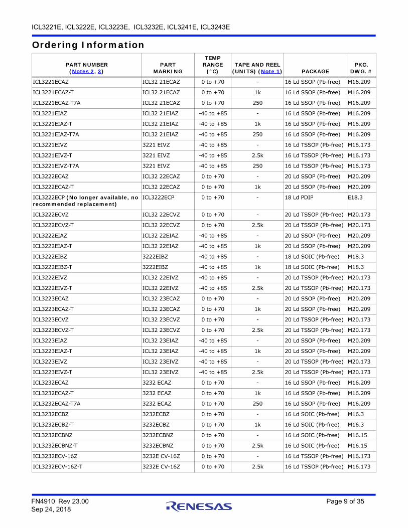
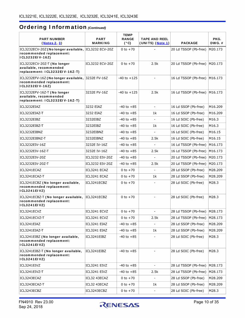
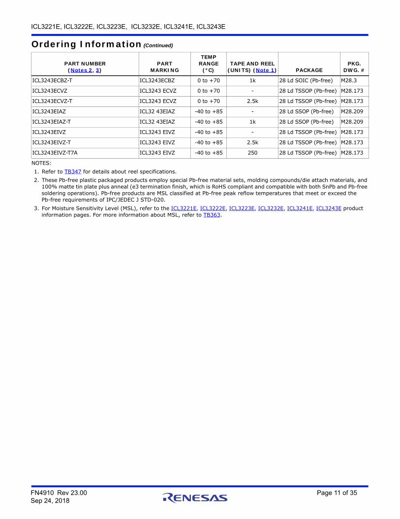
NOTES:1. Refer to TB347 for details about reel specifications.2. These Pb-free plastic packaged products employ special Pb-free material sets, molding compounds/die attach materials, and
100% matte tin plate plus anneal (e3 termination finish, which is RoHS compliant and compatible with both SnPb and Pb-free soldering operations). Pb-free products are MSL classified at Pb-free peak reflow temperatures that meet or exceed the Pb-free requirements of IPC/JEDEC J STD-020.
3. For Moisture Sensitivity Level (MSL), refer to the ICL3221E, ICL3222E, ICL3223E, ICL3232E, ICL3241E, ICL3243E product information pages. For more information about MSL, refer to TB363.
Maximum Junction Temperature (Plastic Package) . +150°CMaximum Storage Temperature Range . . . -65°C to +150°CPb-Free Reflow Profile . . . . . . . . . . . . . . . . . . . . see TB493
CAUTION: Do not operate at or near the maximum ratings listed for extended periods of time. Exposure to such conditions can adversely impactproduct reliability and result in failures not covered by warranty.
NOTE:4. JA is measured with the component mounted on a low-effective thermal conductivity test board in free air. See TB379 for
details.
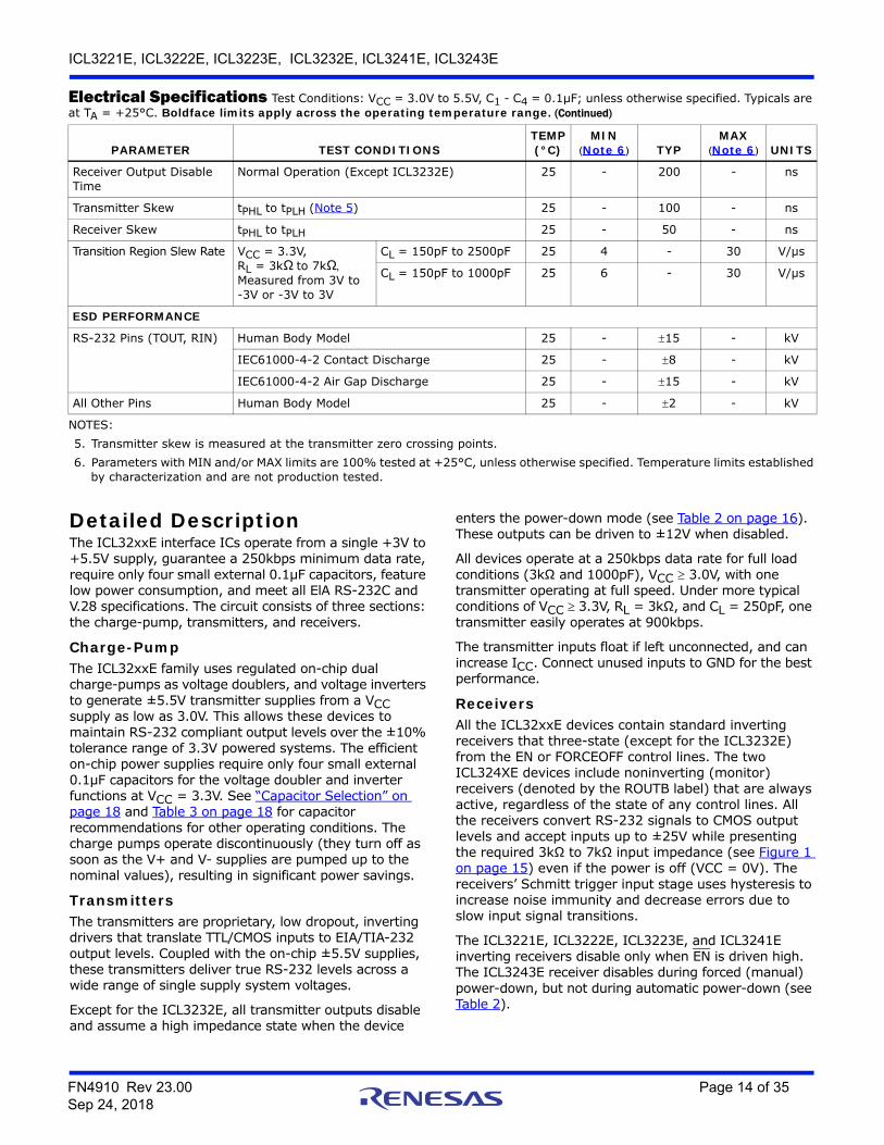
Electrical Specifications Test Conditions: VCC = 3.0V to 5.5V, C1 - C4 = 0.1µF; unless otherwise specified. Typicals are at TA = +25°C. Boldface limits apply across the operating temperature range.
PARAMETER TEST CONDITIONSTEMP(°C)
MIN(Note 6) TYP
MAX(Note 6) UNITS
DC CHARACTERISTICS
Supply Current, Automatic Power-Down
All RIN Open, FORCEON = GND, FORCEOFF = VCC(ICL3221E, ICL3223E, ICL3243E Only)
Electrical Specifications Test Conditions: VCC = 3.0V to 5.5V, C1 - C4 = 0.1µF; unless otherwise specified. Typicals are at TA = +25°C. Boldface limits apply across the operating temperature range. (Continued)
Detailed DescriptionThe ICL32xxE interface ICs operate from a single +3V to +5.5V supply, guarantee a 250kbps minimum data rate, require only four small external 0.1µF capacitors, feature low power consumption, and meet all ElA RS-232C and V.28 specifications. The circuit consists of three sections: the charge-pump, transmitters, and receivers.
Charge-PumpThe ICL32xxE family uses regulated on-chip dual charge-pumps as voltage doublers, and voltage inverters to generate ±5.5V transmitter supplies from a VCC supply as low as 3.0V. This allows these devices to maintain RS-232 compliant output levels over the ±10% tolerance range of 3.3V powered systems. The efficient on-chip power supplies require only four small external 0.1µF capacitors for the voltage doubler and inverter functions at VCC = 3.3V. See “Capacitor Selection” on page 18 and Table 3 on page 18 for capacitor recommendations for other operating conditions. The charge pumps operate discontinuously (they turn off as soon as the V+ and V- supplies are pumped up to the nominal values), resulting in significant power savings.
TransmittersThe transmitters are proprietary, low dropout, inverting drivers that translate TTL/CMOS inputs to EIA/TIA-232 output levels. Coupled with the on-chip ±5.5V supplies, these transmitters deliver true RS-232 levels across a wide range of single supply system voltages.
Except for the ICL3232E, all transmitter outputs disable and assume a high impedance state when the device
enters the power-down mode (see Table 2 on page 16). These outputs can be driven to ±12V when disabled.
All devices operate at a 250kbps data rate for full load conditions (3kΩ and 1000pF), VCC 3.0V, with one transmitter operating at full speed. Under more typical conditions of VCC 3.3V, RL = 3kΩ, and CL = 250pF, one transmitter easily operates at 900kbps.
The transmitter inputs float if left unconnected, and can increase ICC. Connect unused inputs to GND for the best performance.
ReceiversAll the ICL32xxE devices contain standard inverting receivers that three-state (except for the ICL3232E) from the EN or FORCEOFF control lines. The two ICL324XE devices include noninverting (monitor) receivers (denoted by the ROUTB label) that are always active, regardless of the state of any control lines. All the receivers convert RS-232 signals to CMOS output levels and accept inputs up to ±25V while presenting the required 3kΩ to 7kΩ input impedance (see Figure 1 on page 15) even if the power is off (VCC = 0V). The receivers’ Schmitt trigger input stage uses hysteresis to increase noise immunity and decrease errors due to slow input signal transitions.
The ICL3221E, ICL3222E, ICL3223E, and ICL3241E inverting receivers disable only when EN is driven high. The ICL3243E receiver disables during forced (manual) power-down, but not during automatic power-down (see Table 2).
Transition Region Slew Rate VCC = 3.3V, RL = 3kΩto 7kΩMeasured from 3V to -3V or -3V to 3V
CL = 150pF to 2500pF 25 4 - 30 V/µs
CL = 150pF to 1000pF 25 6 - 30 V/µs
ESD PERFORMANCE
RS-232 Pins (TOUT, RIN) Human Body Model 25 - 15 - kV
IEC61000-4-2 Contact Discharge 25 - 8 - kV
IEC61000-4-2 Air Gap Discharge 25 - 15 - kV
All Other Pins Human Body Model 25 - 2 - kV
NOTES:5. Transmitter skew is measured at the transmitter zero crossing points.6. Parameters with MIN and/or MAX limits are 100% tested at +25°C, unless otherwise specified. Temperature limits established
by characterization and are not production tested.
Electrical Specifications Test Conditions: VCC = 3.0V to 5.5V, C1 - C4 = 0.1µF; unless otherwise specified. Typicals are at TA = +25°C. Boldface limits apply across the operating temperature range. (Continued)
The ICL3241E and ICL3243E monitor receivers remain active even during manual power-down and forced receiver disable, making them extremely useful for Ring Indicator monitoring. Standard receivers driving powered down peripherals must be disabled to prevent current flow through the peripheral’s protection diodes (see Figures 2 and 3). This renders them useless for wake up functions, but the corresponding monitor receiver can be dedicated to this task, as shown in Figure 3.
Low Power OperationThese 3V devices require a nominal supply current of 0.3mA, even at VCC = 5.5V, during normal operation (not in power-down mode). This is considerably less than the 5mA to 11mA current required by comparable 5V RS-232 devices, allowing users to reduce system power simply by switching to this family.
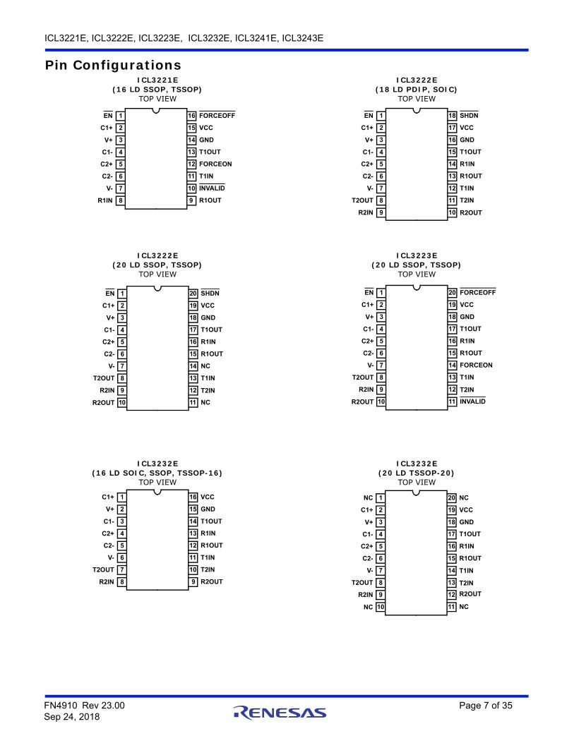
Pin-Compatible Replacements for 5V DevicesThe ICL3221E, ICL3222E, ICL3232E are pin-compatible with existing 5V RS-232 transceivers. See “Features” on page 1 for more information.
The pin compatibility coupled with the low ICC and wide operating supply range make the ICL32xxE potential lower power, higher performance drop-in replacements for existing 5V applications. As long as the 5V RS-232 output swings are acceptable, and transmitter input pull-up resistors are not required, the ICL32xxE works in most 5V applications.
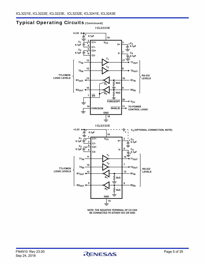
When replacing a device in an existing 5V application, you can terminate C3 to VCC as shown in the “Typical Operating Circuits” on page 4. If possible, terminate C3 to GND for slightly better performance.
Power-Down Functionality (Except ICL3232E)The already low current requirement drops significantly when the device enters power-down mode. In power-down, supply current drops to 1µA because the on-chip charge pump turns off (V+ collapses to VCC and V- collapses to GND), and the transmitter outputs three-state. Inverting receiver outputs may or may not disable in power-down; refer to Table 2 for details. This micro-power mode makes these devices ideal for battery powered and portable applications.
Software Controlled (Manual) Power-DownMost devices in the ICL32xxE family provide pins that allow the user to force the IC into the low power, standby state.
On the ICL3222E and ICL3241E, the power-down control is a simple shutdown (SHDN) pin. Driving this pin high enables normal operation, while driving it low forces the IC into its power-down state. Connect SHDN to VCC if the power-down function is not needed. Note that all the receiver outputs remain enabled during shutdown (see Table 2). For the lowest power consumption during power-down, the receivers should also be disabled by driving the EN input high (see “Receiver ENABLE Control (ICL3221E, ICL3222E, ICL3223E, and ICL3241E Only)” on page 18, and Figures 2 and 3).
The ICL3221E, ICL3223E, and ICL3243E use a two pin approach in which the FORCEON and FORCEOFF inputs determine the IC’s mode. For always enabled operation, FORCEON and FORCEOFF are both strapped high. To switch between active and power-down modes, under logic or software control, only the FORCEOFF input needs
RXOUT
GND VROUT VCC5kΩ
RXIN
-25V VRIN +25V
GND
VCC
FIGURE 1. INVERTING RECEIVER CONNECTIONS
FIGURE 2. POWER DRAIN THROUGH POWERED DOWN PERIPHERAL
to be driven. The FORCEON state is not critical, as FORCEOFF overrides FORCEON. However, if strictly manual control over power-down is desired, the user must strap FORCEON high to disable the automatic power-down circuitry. The ICL3243E inverting (standard)
receiver outputs also disable when the device is in manual power-down, eliminating the possible current path through a shutdown peripheral’s input protection diode (see Figures 2 and 3).
The INVALID output always indicates whether a valid RS-232 signal is present at any of the receiver inputs (see Table 2), providing an easy way to determine when the interface block should power down. If an interface cable is disconnected and all the receiver inputs are floating (but pulled to GND by the internal receiver pull down resistors), the INVALID logic detects the invalid levels
and drives the output low. The power management logic then uses this indicator to power down the interface block. Reconnecting the cable restores valid levels at the receiver inputs, INVALID switches high, and the power management logic wakes up the interface block. INVALID can also indicate the DTR or RING INDICATOR signal, as long as the other receiver inputs are floating or driven to
TABLE 2. POWER-DOWN AND ENABLE LOGIC TRUTH TABLE
RS-232SIGNAL
PRESENT ATRECEIVERINPUT?
FORCEOFFOR SHDN
INPUTFORCEON
INPUTEN
INPUTTRANSMITTER
OUTPUTSRECEIVEROUTPUTS
ROUTBOUTPUTS(Note 7)
INVALIDOUTPUT
MODE OF OPERATION
ICL3222E, ICL3241E
N/A L N/A L High-Z Active Active N/A Manual Power-Down
N/A L N/A H High-Z High-Z Active N/A Manual Power-Down with Receiver Disabled
N/A H N/A L Active Active Active N/A Normal Operation
N/A H N/A H Active High-Z Active N/A Normal Operation withReceiver Disabled
ICL3221E, ICL3223E
No H H L Active Active N/A L Normal Operation(Auto Power-Down Disabled)
No H H H Active High-Z N/A L
Yes H L L Active Active N/A H Normal Operation(Auto Power-Down Enabled)
Yes H L H Active High-Z N/A H
No H L L High-Z Active N/A L Power-Down Due to Auto Power-Down Logic
No H L H High-Z High-Z N/A L
Yes L X L High-Z Active N/A H Manual Power-Down
Yes L X H High-Z High-Z N/A H Manual Power-Down with Receiver Disabled
No L X L High-Z Active N/A L Manual Power-Down
No L X H High-Z High-Z N/A L Manual Power-Down with Receiver Disabled
ICL3243E
No H H N/A Active Active Active L Normal Operation(Auto Power-Down Disabled)
Yes H L N/A Active Active Active H Normal Operation(Auto Power-Down Enabled)
No H L N/A High-Z Active Active L Power-Down Due to Auto Power-Down Logic
Yes L X N/A High-Z High-Z Active H Manual Power-Down
No L X N/A High-Z High-Z Active L Manual Power-Down
NOTE:7. Applies only to the ICL3241E and ICL3243E.
GND (as in the case of a powered down driver). Connecting FORCEOFF and FORCEON together disables the automatic power-down feature, enabling them to function as a manual SHUTDOWN input (see Figure 4).
With any of the control schemes, the time required to exit power-down and resume transmission is 100µs. A mouse or other application may need more time to wake up from shutdown. If automatic power-down is used, the RS-232 device reenters power-down if valid receiver levels are not reestablished within 30µs of the ICL32xxE powering up. Figure 5 illustrates a circuit that keeps the ICL32xxE from initiating automatic power-down for 100ms after powering up. This gives the slow-to-wake peripheral circuit time to reestablish valid RS-232 output levels.
Automatic Power-Down (ICL3221E, ICL3223E, and ICL3243E Only)Even greater power savings are available by using the devices that feature an automatic power-down function. When no valid RS-232 voltages are sensed on any receiver input for 30µs (see Figure 6), the charge pump and transmitters power down, reducing supply current to 1µA. Invalid receiver levels occur whenever the driving peripheral’s outputs are shut off (powered down) or when the RS-232 interface cable is disconnected. The ICL32xxE powers back up whenever it detects a valid RS-232 voltage level on any receiver input. This automatic power-down feature provides additional system power savings without changes to the existing operating system.
Automatic power-down operates when the FORCEON input is low and the FORCEOFF input is high. Tying FORCEON high disables automatic power-down, but manual power-down is always available with the overriding FORCEOFF input. Table 2 on page 16 summarizes the automatic power-down functionality.
FIGURE 4. CONNECTIONS FOR MANUAL POWER-DOWN WHEN NO VALID RECEIVER SIGNALS ARE PRESENT
PWR
FORCEOFF
INVALID
CPU
I/O
FORCEON
ICL3221E,
MGTLOGIC
UART
ICL3243EICL3223E,
FIGURE 5. CIRCUIT TO PREVENT AUTO POWER-DOWN FOR 100ms AFTER FORCED POWER-UP
ICL3221E, ICL3223E, ICL3243E
FORCEOFF FORCEON
POWER MASTER POWER-DOWN LINE
1MΩ0.1µFMANAGEMENT
UNIT
FIGURE 6. DEFINITION OF VALID RS-232 RECEIVER LEVELS
Devices with the automatic power-down feature include an INVALID output signal, which switches low to indicate that invalid levels have persisted on all of the receiver inputs for more than 30µs (see Figure 7). INVALID switches high 1µs after detecting a valid RS-232 level on a receiver input. INVALID operates in all modes (forced or automatic power-down, or forced on), so it is also useful for systems employing manual power-down circuitry. When automatic power-down is utilized, INVALID = 0 indicates that the ICL32xxE is in power-down mode.
The time to recover from automatic power-down mode is typically 100µs.
Receiver ENABLE Control (ICL3221E, ICL3222E, ICL3223E, and ICL3241E Only)The ICL3221E, ICL3222E, ICL3223E, and ICL3241E also feature an EN input to control the receiver outputs. Driving EN high disables all the inverting (standard) receiver outputs, placing them in a high impedance state. This is useful for eliminating supply current, due to a receiver output forward biasing the protection diode, when driving the input of a powered down (VCC = GND) peripheral (see Figure 2 on page 15). The enable input has no effect on transmitter or monitor (ROUTB) outputs.
Capacitor SelectionThe charge pumps require 0.1µF capacitors for 3.3V operation. For other supply voltages, refer to Table 3 for capacitor values. Do not use values smaller than those listed in Table 3. Increasing the capacitor values (by a factor of 2) reduces ripple on the transmitter outputs and slightly reduces power consumption. C2, C3, and C4 can be increased without increasing C1’s value; however, do not increase C1 without also increasing C2, C3, and C4 to maintain the proper ratios (C1 to the other capacitors).
When using minimum required capacitor values, make sure that capacitor values do not degrade excessively with temperature. If in doubt, use capacitors with a larger nominal value. The capacitor’s Equivalent Series
Resistance (ESR) usually rises at low temperatures and it influences the amount of ripple on V+ and V-.
Power Supply DecouplingIn most circumstances, a 0.1µF bypass capacitor is adequate. In applications that are particularly sensitive to power supply noise, decouple VCC to ground with a capacitor of the same value as the charge-pump capacitor C1. Connect the bypass capacitor as close as possible to the IC.
Operation Down to 2.7VThe ICL32xxE transmitter outputs meet RS-562 levels (±3.7V) at full data rate, with VCC as low as 2.7V. RS-562 levels typically ensure interoperability with RS-232 devices.
Transmitter Outputs when Exiting Power-DownFigure 8 shows the response of two transmitter outputs when exiting power-down mode. As they activate, the two transmitter outputs properly go to opposite RS-232 levels, with no glitching, ringing, or undesirable transients. Each transmitter is loaded with 3kΩin parallel with 2500pF. Note that the transmitters enable only when the magnitude of the supplies exceeds approximately 3V.
Mouse DriveabilityThe ICL3241E and ICL3243E have been specifically designed to power a serial mouse while operating from low voltage supplies. Figure 9 on page 19 shows the transmitter output voltages under increasing load
RECEIVER
INPUTS
TRANSMITTEROUTPUTS
INVALID
OUTPUT
V+
VCC
0
V-
VCC
0
tINVL tINVH
INVALIDREGION}
FIGURE 7. AUTOMATIC POWER-DOWN AND INVALID TIMING DIAGRAMS
AUTOPWDN PWR UP
TABLE 3. REQUIRED CAPACITOR VALUES
VCC(V)
C1(µF)
C2, C3, C4(µF)
3.0 to 3.6 0.1 0.1
4.5 to 5.5 0.047 0.33
3.0 to 5.5 0.1 0.47
TIME (20µs/DIV)
T1
T2
2V/DIV
5V/DIV
VCC = +3.3V
FORCEOFF
FIGURE 8. TRANSMITTER OUTPUTS WHEN EXITING POWER-DOWN
current. The on-chip switching regulator ensures the transmitters supply at least 5V during worst case conditions (15mA for paralleled V+ transmitters, 7.3mA for a single V- transmitter). The Automatic Power-Down feature does not work with a mouse, so FORCEOFF and FORCEON should be connected to VCC.
High Data RatesThe ICL32xxE devices maintain the RS-232 5V minimum transmitter output voltages even at high data rates. Figure 10 details a transmitter loopback test circuit, and Figure 11 illustrates the loopback test result at 120kbps. For this test, all transmitters were simultaneously driving RS-232 loads in parallel with 1000pF at 120kbps. Figure 12 shows the loopback results for a single transmitter driving 1000pF and an RS-232 load at 250kbps. The static transmitters were also loaded with an RS-232 receiver. Interconnection with 3V and 5V
LogicThe ICL32XX devices directly interface with 5V CMOS and TTL logic families. The AC, HC, and CD4000 outputs can drive ICL32XX inputs with the ICL32XX at 3.3V and the logic supply at 5V, but ICL32XX outputs do not reach the minimum VIH for these logic families. See Table 4.
FIGURE 10. TRANSMITTER LOOPBACK TEST CIRCUIT
FIGURE 9. TRANSMITTER OUTPUT VOLTAGE vs LOAD CURRENT (PER TRANSMITTER, DOUBLE CURRENT AXIS FOR TOTAL VOUT+ CURRENT)
TR
AN
SM
ITT
ER
OU
TP
UT
VO
LTA
GE
(V
)
LOAD CURRENT PER TRANSMITTER (mA)
0 2 4 6 8 10-6
-4
-2
0
2
4
6
-5
-3
-1
1
3
5
1 3 5 7 9
VOUT+
VOUT -VCC
VOUT+
VOUT -
T1
T2
T3
VCC = 3.0V
ICL3241E, ICL3243E
ICL32xxE
VCCFORCEOFF
C1
C2C4
C3
+
++
+
1000pF
V+
V-
5K
TIN
ROUT
C1+
C1-
C2+
C2-
RIN
TOUT
+VCC
0.1µF
VCC
EN
SHDN OR
FIGURE 11. LOOPBACK TEST AT 120kbps
FIGURE 12. LOOPBACK TEST AT 250kbps
TABLE 4. LOGIC FAMILY COMPATIBILITY WITH VARIOUS SUPPLY VOLTAGES
SYSTEM POWER-SUPPLY
VOLTAGE (V)
VCC SUPPLY
VOLTAGE (V) COMPATIBILITY
3.3 3.3 Compatible with all CMOS families
5 5 Compatible with all TTL and CMOS logic families
5 3.3 Compatible with ACT and HCT CMOS, and with TTL. ICL32XX outputs are incompatible with AC, HC, and CD4000 CMOS inputs
±15kV ESD ProtectionAll pins on ICL32XX devices include ESD protection structures, but the ICL32xxE family incorporates advanced structures that allow the RS-232 pins (transmitter outputs and receiver inputs) to survive ESD events up to ±15kV. The RS-232 pins are particularly vulnerable to ESD damage because they typically connect to an exposed port on the exterior of the finished product. Simply touching the port pins, or connecting a cable, can cause an ESD event that might destroy unprotected ICs. The ESD structures protect the device whether or not it is powered up, protect without allowing any latch-up mechanism to activate, and do not interfere with RS-232 signals as large as ±25V.
Human Body Model (HBM) TestingThis test method emulates the ESD event delivered to an IC during human handling. The tester delivers the charge through a 1.5kΩ current limiting resistor, making the test less severe than the IEC61000 test which utilizes a 330Ω limiting resistor. The HBM method determines an IC’s ability to withstand the ESD transients typically present during handling and manufacturing. Due to the random nature of these events, each pin is tested with respect to all other pins. The RS-232 pins on “E” family devices can withstand HBM ESD events to ±15kV.
IEC61000-4-2 TestingThe IEC61000 test method applies to finished equipment, rather than to an individual IC. Therefore, the pins most likely to suffer an ESD event are those that are exposed to the outside world (the RS-232 pins in this case), and the IC is tested in its typical application configuration (power applied) rather than testing each pin-to-pin combination. The lower current limiting resistor coupled with the larger charge storage capacitor yields a test that is much more severe than the HBM test. The extra ESD protection built into this device’s RS-232 pins allows the design of equipment meeting level 4 criteria without the need for additional board level protection on the RS-232 port.
AIR-GAP DISCHARGE TEST METHODFor this test method, a charged probe tip moves toward the IC pin until the voltage arcs to it. The current waveform delivered to the IC pin depends on approach speed, humidity, temperature, etc., so it is difficult to obtain repeatable results. The “E” device RS-232 pins withstand ±15kV air-gap discharges.
CONTACT DISCHARGE TEST METHODDuring the contact discharge test, the probe contacts the tested pin before the probe tip is energized, thereby eliminating the variables associated with the air-gap discharge. The result is a more repeatable and predictable test, but equipment limits prevent testing devices at voltages higher than ±8kV. All “E” family devices survive ±8kV contact discharges on the RS-232 pins.
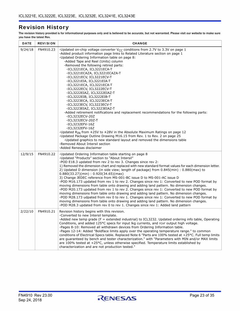
Revision HistoryThe revision history provided is for informational purposes only and is believed to be accurate, but not warranted. Please visit our website to make sure you have the latest Rev.
DATE REVISION CHANGE
9/24/18 FN4910.23 -Updated on-chip voltage converter VCC conditions from 2.7V to 3.3V on page 1-Added product information page links to Related Literature section on page 1-Updated Ordering Information table on page 8:
-Added Tape and Reel (Units) column-Removed the following retired parts:
-Added retirement notifications and replacement recommendations for the following parts:-ICL3232ECV-20Z-ICL3232ECV-20Z-T-ICL3232EFV-16Z-ICL3232EFV-16Z
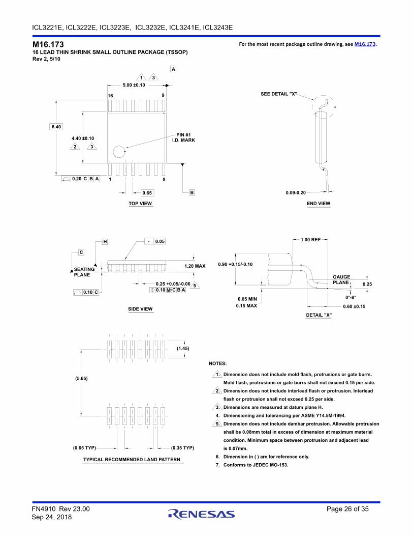
-Updated RIN from ±25V to ±28V in the Absolute Maximum Ratings on page 12-Updated Package Outline Drawing M16.15 from Rev. 1 to Rev. 2 on page 25
-Updated graphics to new standard layout and removed the dimensions table-Removed About Intersil section-Added Renesas disclaimer
12/9/15 FN4910.22 -Updated Ordering Information table starting on page 8-Updated “Products” section to “About Intersil”-POD E18.3 updated from rev 2 to rev 3. Changes since rev 2:1) Removed the dimension chart and replaced with new standard format values for each dimension letter. 2) Updated D dimension (in side view; length of package) from 0.845(min) : 0.880(max) to 0.880(33.27)(min) : 0.920(34.65)(max) 3) Change JEDEC reference from MS-001-BC issue D to MS-001-AC issue D-POD M16.173 updated from rev 1 to rev 2. Changes since rev 1: Converted to new POD format by moving dimensions from table onto drawing and adding land pattern. No dimension changes.-POD M20.173 updated from rev 1 to rev 2. Changes since rev 1: Converted to new POD format by moving dimensions from table onto drawing and adding land pattern. No dimension changes.-POD M28.173 udpated from rev 0 to rev 1. Changes since rev 1: Converted to new POD format by moving dimensions from table onto drawing and adding land pattern. No dimension changes.-POD M28.3 updated from rev 0 to rev 1. Changes since rev 1: Added land pattern
2/22/10 FN4910.21 Revision history begins with this revision.-Converted to new Intersil template.-Added new temp grade (F = extended industrial) to ICL3232. Updated ordering info table, Operating Conditions, and added 125°C specs for input lkg currents, and rcvr output high voltage. -Pages 8-10: Removed all withdrawn devices from Ordering Information table.-Pages 12-14: Added "Boldface limits apply over the operating temperature range." to common conditions of Electrical Specs table. Replaced Note 6 "Parts are 100% tested at +25°C. Full temp limits are guaranteed by bench and tester characterization." with "Parameters with MIN and/or MAX limits are 100% tested at +25°C, unless otherwise specified. Temperature limits established by characterization and are not production tested."
1. Symbols are defined in the “MO Series Symbol List” in Section 2.2 of Publication Number 95.
2. Dimensioning and tolerancing per ANSI Y14.5M-1982.
3. Dimension “D” does not include mold flash, protrusions or gate burrs. Mold flash, protrusion and gate burrs shall not exceed 0.20mm (0.0078inch) per side.
4. Dimension “E” does not include interlead flash or protrusions. Interlead flash and protrusions shall not exceed 0.20mm (0.0078 inch) per side.
5. The chamfer on the body is optional. If it is not present, a visual index feature must be located within the crosshatched area.
6. “L” is the length of terminal for soldering to a substrate.
7. “N” is the number of terminal positions.
8. Terminal numbers are shown for reference only.
9. Dimension “B” does not include dambar protrusion. Allowable dambar protrusion shall be 0.13mm (0.005 inch) total in excess of “B” dimen-sion at maximum material condition.
10. Controlling dimension: MILLIMETER. Converted inch dimensions are not necessarily exact.
INDEXAREA
E
D
N
1 2 3
-B-
0.25(0.010) C AM B S
e
-A-
L
B
M
-C-
A1
A
SEATING PLANE
0.10(0.004)
C
H 0.25(0.010) BM M
0.250.010
GAUGEPLANE
A2
M16.209 (JEDEC MO-150-AC ISSUE B)16 LEAD SHRINK SMALL OUTLINE PLASTIC PACKAGE
SYMBOL
INCHES MILLIMETERS
NOTESMIN MAX MIN MAX
A - 0.078 - 2.00 -
A1 0.002 - 0.05 - -
A2 0.065 0.072 1.65 1.85 -
B 0.009 0.014 0.22 0.38 9
C 0.004 0.009 0.09 0.25 -
D 0.233 0.255 5.90 6.50 3
E 0.197 0.220 5.00 5.60 4
e 0.026 BSC 0.65 BSC -
H 0.292 0.322 7.40 8.20 -
L 0.022 0.037 0.55 0.95 6
N 16 16 7
0° 8° 0° 8° -
Rev. 3 6/05
For the most recent package outline drawing, see M16.209.
1. Symbols are defined in the “MO Series Symbol List” in Section 2.2 of Publication Number 95.
2. Dimensioning and tolerancing per ANSI Y14.5M-1982.
3. Dimension “D” does not include mold flash, protrusions or gate burrs. Mold flash, protrusion and gate burrs shall not exceed 0.15mm (0.006inch) per side.
4. Dimension “E” does not include interlead flash or protrusions. Interlead flash and protrusions shall not exceed 0.25mm (0.010 inch) per side.
5. The chamfer on the body is optional. If it is not present, a visual index feature must be located within the crosshatched area.
6. “L” is the length of terminal for soldering to a substrate.
7. “N” is the number of terminal positions.
8. Terminal numbers are shown for reference only.
9. The lead width “B”, as measured 0.36mm (0.014 inch) or greater above the seating plane, shall not exceed a maximum value of 0.61mm (0.024inch)
10. Controlling dimension: MILLIMETER. Converted inch dimensions are not necessarily exact.
INDEXAREA
E
D
N
1 2 3
-B-
0.25(0.010) C AM B S
e
-A-
L
B
M
-C-
A1
A
SEATING PLANE
0.10(0.004)
h x 45°
C
H 0.25(0.010) BM M
M16.3 (JEDEC MS-013-AA ISSUE C)16 LEAD WIDE BODY SMALL OUTLINE PLASTIC PACKAGE
SYMBOL
INCHES MILLIMETERS
NOTESMIN MAX MIN MAX
A 0.0926 0.1043 2.35 2.65 -
A1 0.0040 0.0118 0.10 0.30 -
B 0.013 0.0200 0.33 0.51 9
C 0.0091 0.0125 0.23 0.32 -
D 0.3977 0.4133 10.10 10.50 3
E 0.2914 0.2992 7.40 7.60 4
e 0.050 BSC 1.27 BSC -
H 0.394 0.419 10.00 10.65 -
h 0.010 0.029 0.25 0.75 5
L 0.016 0.050 0.40 1.27 6
N 16 16 7
0° 8° 0° 8° -
Rev. 1 6/05
For the most recent package outline drawing, see M16.3.
1. Symbols are defined in the “MO Series Symbol List” in Section 2.2 of Publication Number 95.
2. Dimensioning and tolerancing per ANSI Y14.5M-1982.
3. Dimension “D” does not include mold flash, protrusions or gate burrs. Mold flash, protrusion and gate burrs shall not exceed 0.15mm (0.006inch) per side.
4. Dimension “E” does not include interlead flash or protrusions. Interlead flash and protrusions shall not exceed 0.25mm (0.010 inch) per side.
5. The chamfer on the body is optional. If it is not present, a visual index feature must be located within the crosshatched area.
6. “L” is the length of terminal for soldering to a substrate.
7. “N” is the number of terminal positions.
8. Terminal numbers are shown for reference only.
9. The lead width “B”, as measured 0.36mm (0.014 inch) or greater above the seating plane, shall not exceed a maximum value of 0.61mm(0.024 inch)
10. Controlling dimension: MILLIMETER. Converted inch dimensions are not necessarily exact.
INDEXAREA
E
D
N
1 2 3
-B-
0.25(0.010) C AM B S
e
-A-
L
B
M
-C-
A1
A
SEATING PLANE
0.10(0.004)
h x 45°
C
H 0.25(0.010) BM M
M18.3 (JEDEC MS-013-AB ISSUE C)18 LEAD WIDE BODY SMALL OUTLINE PLASTIC PACKAGE
SYMBOL
INCHES MILLIMETERS
NOTESMIN MAX MIN MAX
A 0.0926 0.1043 2.35 2.65 -
A1 0.0040 0.0118 0.10 0.30 -
B 0.013 0.0200 0.33 0.51 9
C 0.0091 0.0125 0.23 0.32 -
D 0.4469 0.4625 11.35 11.75 3
E 0.2914 0.2992 7.40 7.60 4
e 0.050 BSC 1.27 BSC -
H 0.394 0.419 10.00 10.65 -
h 0.010 0.029 0.25 0.75 5
L 0.016 0.050 0.40 1.27 6
N 18 18 7
0° 8° 0° 8° -
Rev. 1 6/05
For the most recent package outline drawing, see M18.3.
1. Symbols are defined in the “MO Series Symbol List” in Section 2.2 of Publication Number 95.
2. Dimensioning and tolerancing per ANSI Y14.5M-1982.
3. Dimension “D” does not include mold flash, protrusions or gate burrs. Mold flash, protrusion and gate burrs shall not exceed0.20mm (0.0078 inch) per side.
4. Dimension “E” does not include interlead flash or protrusions. In-terlead flash and protrusions shall not exceed 0.20mm (0.0078inch) per side.
5. The chamfer on the body is optional. If it is not present, a visual index feature must be located within the crosshatched area.
6. “L” is the length of terminal for soldering to a substrate.
7. “N” is the number of terminal positions.
8. Terminal numbers are shown for reference only.
9. Dimension “B” does not include dambar protrusion. Allowable dambar protrusion shall be 0.13mm (0.005 inch) total in excessof “B” dimension at maximum material condition.
10. Controlling dimension: MILLIMETER. Converted inch dimen-sions are not necessarily exact.
INDEXAREA
E
D
N
1 2 3
-B-
0.25(0.010) C AM B S
e
-A-
B
M
-C-
A1
A
SEATING PLANE
0.10(0.004)
C
H 0.25(0.010) BM M
L0.250.010
GAUGEPLANE
A2
M20.209 (JEDEC MO-150-AE ISSUE B)20 LEAD SHRINK SMALL OUTLINE PLASTIC PACKAGE
SYMBOL
INCHES MILLIMETERS
NOTESMIN MAX MIN MAX
A 0.068 0.078 1.73 1.99
A1 0.002 0.008’ 0.05 0.21
A2 0.066 0.070’ 1.68 1.78
B 0.010’ 0.015 0.25 0.38 9
C 0.004 0.008 0.09 0.20’
D 0.278 0.289 7.07 7.33 3
E 0.205 0.212 5.20’ 5.38 4
e 0.026 BSC 0.65 BSC
H 0.301 0.311 7.65 7.90’
L 0.025 0.037 0.63 0.95 6
N 20 20 7
0 deg. 8 deg. 0 deg. 8 deg.
Rev. 3 11/02
For the most recent package outline drawing, see M20.209.
1. Symbols are defined in the “MO Series Symbol List” in Section 2.2 of Publication Number 95.
2. Dimensioning and tolerancing per ANSI Y14.5M-1982.
3. Dimension “D” does not include mold flash, protrusions or gate burrs. Mold flash, protrusion and gate burrs shall not exceed 0.20mm (0.0078 inch) per side.
4. Dimension “E” does not include interlead flash or protrusions. Interlead flash and protrusions shall not exceed 0.20mm (0.0078 inch) per side.
5. The chamfer on the body is optional. If it is not present, a visual index feature must be located within the crosshatched area.
6. “L” is the length of terminal for soldering to a substrate.
7. “N” is the number of terminal positions.
8. Terminal numbers are shown for reference only.
9. Dimension “B” does not include dambar protrusion. Allowable dambar protrusion shall be 0.13mm (0.005 inch) total in excess of “B” dimension at maximum material condition.
10. Controlling dimension: MILLIMETER. Converted inch dimensions are not necessarily exact.
INDEXAREA
E
D
N
1 2 3
-B-
0.25(0.010) C AM B S
e
-A-
L
B
M
-C-
A1
A
SEATING PLANE
0.10(0.004)
C
H 0.25(0.010) BM M
0.250.010
GAUGEPLANE
A2
M28.209 (JEDEC MO-150-AH ISSUE B)28 LEAD SHRINK SMALL OUTLINE PLASTIC PACKAGE
SYMBOL
INCHES MILLIMETERS
NOTESMIN MAX MIN MAX
A - 0.078 - 2.00 -
A1 0.002 - 0.05 - -
A2 0.065 0.072 1.65 1.85 -
B 0.009 0.014 0.22 0.38 9
C 0.004 0.009 0.09 0.25 -
D 0.390 0.413 9.90 10.50 3
E 0.197 0.220 5.00 5.60 4
e 0.026 BSC 0.65 BSC -
H 0.292 0.322 7.40 8.20 -
L 0.022 0.037 0.55 0.95 6
N 28 28 7
0° 8° 0° 8° -
Rev. 2 6/05
For the most recent package outline drawing, see M28.209.
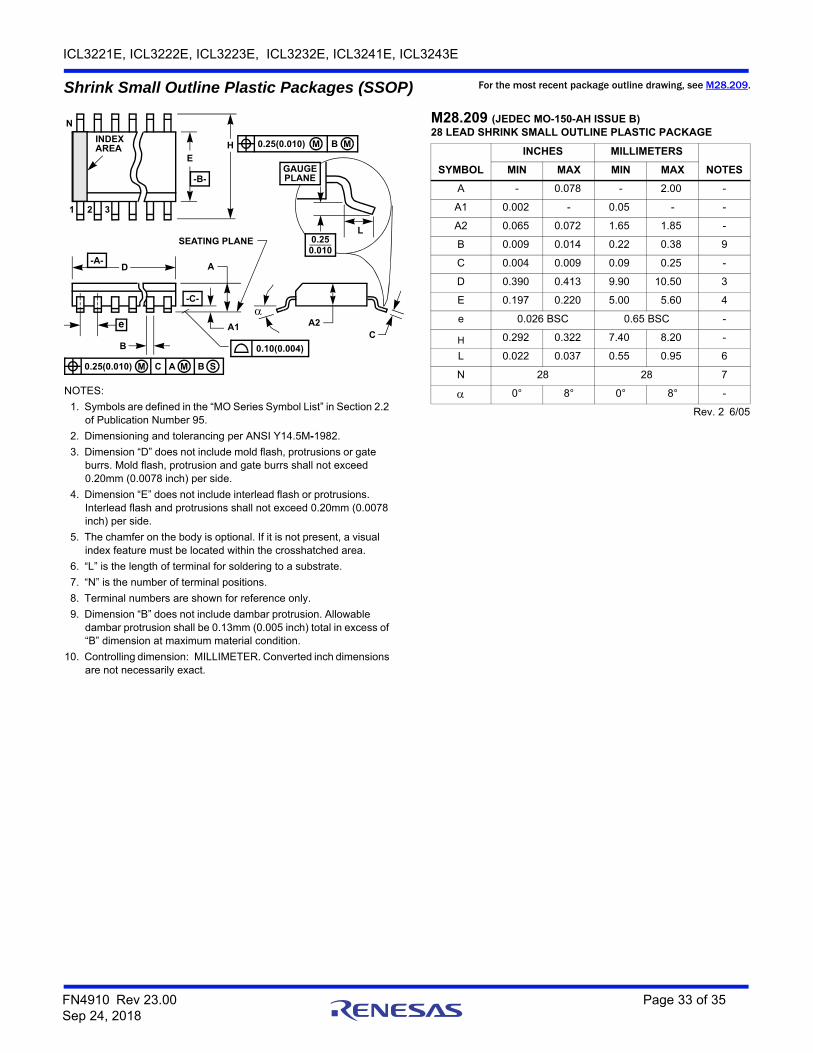
M28.3 (JEDEC MS-013-AE ISSUE C)28 LEAD WIDE BODY SMALL OUTLINE PLASTIC PACKAGE
SYMBOL
INCHES MILLIMETERS
NOTESMIN MAX MIN MAX
A 0.0926 0.1043 2.35 2.65 -
A1 0.0040 0.0118 0.10 0.30 -
B 0.013 0.0200 0.33 0.51 9
C 0.0091 0.0125 0.23 0.32 -
D 0.6969 0.7125 17.70 18.10 3
E 0.2914 0.2992 7.40 7.60 4
e 0.05 BSC 1.27 BSC -
H 0.394 0.419 10.00 10.65 -
h 0.01 0.029 0.25 0.75 5
L 0.016 0.050 0.40 1.27 6
N 28 28 7
0o 8o 0o 8o -
Rev. 1, 1/13
NOTES:
1. Symbols are defined in the “MO Series Symbol List” in Section 2.2 of Publication Number 95.
2. Dimensioning and tolerancing per ANSI Y14.5M-1982.
3. Dimension “D” does not include mold flash, protrusions or gate burrs. Mold flash, protrusion and gate burrs shall not exceed 0.15mm (0.006inch) per side.
4. Dimension “E” does not include interlead flash or protrusions. Interlead flash and protrusions shall not exceed 0.25mm (0.010 inch) per side.
5. The chamfer on the body is optional. If it is not present, a visual index feature must be located within the crosshatched area.
6. “L” is the length of terminal for soldering to a substrate.
7. “N” is the number of terminal positions.
8. Terminal numbers are shown for reference only.
9. The lead width “B”, as measured 0.36mm (0.014 inch) or greater above the seating plane, shall not exceed a maximum value of 0.61mm(0.024 inch)
10. Controlling dimension: MILLIMETER. Converted inch dimensions are not necessarily exact.
For the most recent package outline drawing, see M28.3.
Notice1. Descriptions of circuits, software and other related information in this document are provided only to illustrate the operation of semiconductor products and application examples. You are fully responsible for
the incorporation or any other use of the circuits, software, and information in the design of your product or system. Renesas Electronics disclaims any and all liability for any losses and damages incurred by
you or third parties arising from the use of these circuits, software, or information.
2. Renesas Electronics hereby expressly disclaims any warranties against and liability for infringement or any other claims involving patents, copyrights, or other intellectual property rights of third parties, by or
arising from the use of Renesas Electronics products or technical information described in this document, including but not limited to, the product data, drawings, charts, programs, algorithms, and application
examples.
3. No license, express, implied or otherwise, is granted hereby under any patents, copyrights or other intellectual property rights of Renesas Electronics or others.
4. You shall not alter, modify, copy, or reverse engineer any Renesas Electronics product, whether in whole or in part. Renesas Electronics disclaims any and all liability for any losses or damages incurred by
you or third parties arising from such alteration, modification, copying or reverse engineering.
5. Renesas Electronics products are classified according to the following two quality grades: “Standard” and “High Quality”. The intended applications for each Renesas Electronics product depends on the
product’s quality grade, as indicated below.
"Standard": Computers; office equipment; communications equipment; test and measurement equipment; audio and visual equipment; home electronic appliances; machine tools; personal electronic
equipment; industrial robots; etc.
"High Quality": Transportation equipment (automobiles, trains, ships, etc.); traffic control (traffic lights); large-scale communication equipment; key financial terminal systems; safety control equipment; etc.
Unless expressly designated as a high reliability product or a product for harsh environments in a Renesas Electronics data sheet or other Renesas Electronics document, Renesas Electronics products are
not intended or authorized for use in products or systems that may pose a direct threat to human life or bodily injury (artificial life support devices or systems; surgical implantations; etc.), or may cause
serious property damage (space system; undersea repeaters; nuclear power control systems; aircraft control systems; key plant systems; military equipment; etc.). Renesas Electronics disclaims any and all
liability for any damages or losses incurred by you or any third parties arising from the use of any Renesas Electronics product that is inconsistent with any Renesas Electronics data sheet, user’s manual or
other Renesas Electronics document.
6. When using Renesas Electronics products, refer to the latest product information (data sheets, user’s manuals, application notes, “General Notes for Handling and Using Semiconductor Devices” in the
reliability handbook, etc.), and ensure that usage conditions are within the ranges specified by Renesas Electronics with respect to maximum ratings, operating power supply voltage range, heat dissipation
characteristics, installation, etc. Renesas Electronics disclaims any and all liability for any malfunctions, failure or accident arising out of the use of Renesas Electronics products outside of such specified
ranges.
7. Although Renesas Electronics endeavors to improve the quality and reliability of Renesas Electronics products, semiconductor products have specific characteristics, such as the occurrence of failure at a
certain rate and malfunctions under certain use conditions. Unless designated as a high reliability product or a product for harsh environments in a Renesas Electronics data sheet or other Renesas
Electronics document, Renesas Electronics products are not subject to radiation resistance design. You are responsible for implementing safety measures to guard against the possibility of bodily injury, injury
or damage caused by fire, and/or danger to the public in the event of a failure or malfunction of Renesas Electronics products, such as safety design for hardware and software, including but not limited to
redundancy, fire control and malfunction prevention, appropriate treatment for aging degradation or any other appropriate measures. Because the evaluation of microcomputer software alone is very difficult
and impractical, you are responsible for evaluating the safety of the final products or systems manufactured by you.
8. Please contact a Renesas Electronics sales office for details as to environmental matters such as the environmental compatibility of each Renesas Electronics product. You are responsible for carefully and
sufficiently investigating applicable laws and regulations that regulate the inclusion or use of controlled substances, including without limitation, the EU RoHS Directive, and using Renesas Electronics
products in compliance with all these applicable laws and regulations. Renesas Electronics disclaims any and all liability for damages or losses occurring as a result of your noncompliance with applicable
laws and regulations.
9. Renesas Electronics products and technologies shall not be used for or incorporated into any products or systems whose manufacture, use, or sale is prohibited under any applicable domestic or foreign laws
or regulations. You shall comply with any applicable export control laws and regulations promulgated and administered by the governments of any countries asserting jurisdiction over the parties or
transactions.
10. It is the responsibility of the buyer or distributor of Renesas Electronics products, or any other party who distributes, disposes of, or otherwise sells or transfers the product to a third party, to notify such third
party in advance of the contents and conditions set forth in this document.
11. This document shall not be reprinted, reproduced or duplicated in any form, in whole or in part, without prior written consent of Renesas Electronics.
12. Please contact a Renesas Electronics sales office if you have any questions regarding the information contained in this document or Renesas Electronics products.
(Note 1) “Renesas Electronics” as used in this document means Renesas Electronics Corporation and also includes its directly or indirectly controlled subsidiaries.
(Note 2) “Renesas Electronics product(s)” means any product developed or manufactured by or for Renesas Electronics.


![MAX3221 3-V to 5.5-V RS-232 Line Driver and Receiver … TX POWER APD EN [RX] DIN ROUT DOUT RS232 RIN RS232 1 1 1 1 FORCEON FORCEOFF INVALID STATUS 3.3 V, 5 V Product Folder Sample](https://static.documents.pub/doc/80x56/5ae2df1f7f8b9a495c8c8d92/max3221-3-v-to-55-v-rs-232-line-driver-and-receiver-tx-power-apd-en-rx-din.jpg)