15
Rotary Relay Replacement for the ICOM 720A by KA6BFB
Rotary Relay Replacement
for the
ICOM 720A
by
KA6BFB

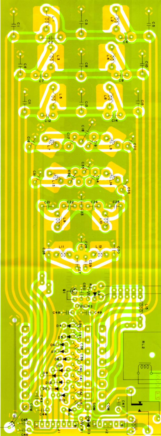
BACKGROUND There are several modifications available for converting the Icom IC-720A rotary relay in the filter module to fixed relays. The most popular ones can be credited to F5IKI and IW9HGS. I have recently finished my own version of this modification. While researching this modification, I noticed some apprehension as well as intimidation because of possible lack of clarity on how to perform the modification. To this end, I tried to take numerous photographs to document my version of this modification. I will try to clearly explain the modification, and my rationale for my version. In my version, most of the components remain on the PCB in the filter module. This results in a drastic reduction in the additional circuitry that is needed. I added the additional circuitry on a small perf-board just above the existing circuitry. This elevated board was held in place with stiff wire wrap pins which also serve a double function of applying three signals to the board. The original circuit by F5IKI in Figure 14 contains three ICs and many discrete components. Chips with 5 volt rails were used with a 5 volt regulator, and then PNP transistors used to level convert outputs where needed to the 7.5V level used in the original circuit. The use of a 4000 series CMOS chip by IW9HGS which can use a rail voltage of 7.5 volts, and a 4017 which contains a counter and decoded in one chip reduced the chip count. This circuit is shown in Figure 15. A NAND gate was used in both versions as filter for the noisy relay pulse signal that drove the NPN transistor that drove the rotary relay. After measuring the signal with the original circuitry, I found the filtering to be adequate as it was. I replaced the original TO-220 package with a smaller 2N2222A. All that was necessary now was to invert and level shift the signal. That is done with another 2N2222A on the board with the 4017. The complete schematic with the existing and additional circuitry is shown in Figure 6. The circuitry inside the dotted rectangles is the new circuitry. MOSFETs were used for the relay drivers instead of bipolar transistors. The reason for this is two-fold. First, there is a lower parts count because base resistors are not required. Second, the gates of the MOSFETs require negligible current, so the outputs of the 4017 are not loaded. This lack of loading means the voltage on the CMOS outputs are very close to the original 7.5 volts provided by the still used Zener regulated supply formed by R1 and D3. The relays are mounted on two boards, one on each side of the low pass filters, as is done with the other modifications. Since there are 7 filters, this means 14 relays are required. I used the same relays as the other modifications. Since these are double pole relays, I theoretically could have used only 7 relays. After some contemplation, I decided that using two poles for the RF power was best. I preferred the redundancy and low stress as a result.

PROCEDURE
Figure 1. Filter Module prior to modification
1) Completely remove the existing rotary relay (RL2). Be careful to leave all other existing components intact. Save the 2 longer brass tubing sections for later use.
Figure 2. Brass tubing from rotary relay 2) Remove D2 and C49. 3) Remove Q1 and replace with a 2N2222A. Be sure to accommodate the different
pin-out of the two transistors. The collector pin is the middle hole. 4) Remove L15 carefully. This inductor will be moved elsewhere to make room for a
relay board. With an insulated piece of wire place on the bottom of the PCB, make a shorting connection to complete the former path of L15.
5) Make a notch in PCB trace as shown in Figure 3. Clear top of PCB on both sides of the notch to expose bare copper on PCB. L15 will be soldered here.
6) Install L15 as shown in Figure 4.
Q1
RL2 L15 C49 D2
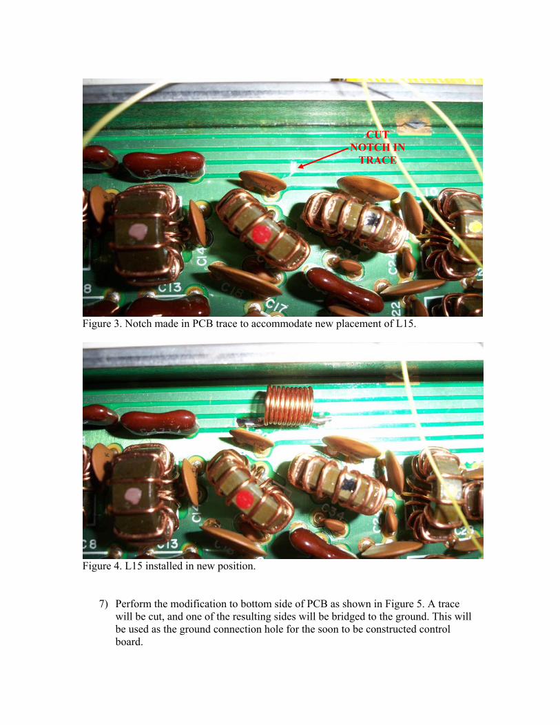
Figure 3. Notch made in PCB trace to accommodate new placement of L15.
Figure 4. L15 installed in new position.
7) Perform the modification to bottom side of PCB as shown in Figure 5. A trace will be cut, and one of the resulting sides will be bridged to the ground. This will be used as the ground connection hole for the soon to be constructed control board.
CUT NOTCH IN
TRACE

Figure 5. Original condition of PCB compared to modified version.
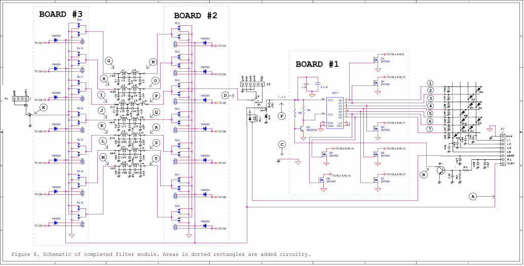
The entire schematic of the completed project is shown in Figure 6. The circuitry inside the dotted rectangles is constructed for this project. The circuitry outside the dotted rectangles is the original Icom circuitry minus the components removed in steps 1 thru 3. Pictures of the final project are shown in Figures 7 and 8.
CUT NOTCH IN
TRACE
BRIDGE TO
GROUND
5
5
4
4
3
3
2
2
1
1
D D
C C
B B
A A
H
S C
D
L
E
N
I
O
F
BOARD #2
7.5V
K
2
M
3
A
5
BOARD #3
1
4
R
T
G
P
7
Q
B
BOARD #1
6
J
Figure 6. Schematic of completed filter module. Areas in dotted rectangles are added circuitry.
TO RL4 & RL11
TO Q7
TO Q3
TO Q5
TO Q3
TO RL3 & RL10
TO RL2 & RL9
TO Q4
TO Q7
TO Q9
TO Q6
TO Q8
TO Q6
TO RL6 & RL13
TO Q5
TO Q9
TO Q4
TO Q8
TO RL5 & RL12TO RL8 & RL15
TO RL7 & RL14
RL6
4017
14
1315
32471015
6
16
8
CLK
ENARST
Q0Q1Q2Q3Q4Q5Q6
Q7
VCC
GND
Q32N7000
RL10
1N4004
RL8
Q72N7000
1N40041N4004
RL12
1N4004
RL9
RL3
Q42N7000
1N4004
1N4004
RL14
Q22N2222A
RL5
4.7 uF
Q92N7000
1N40041N4004
RL7
Q52N7000
Q82N7000
RL11
1N4004
RL2
1N4004
10k
RL15
RL13
10k
1N4004
RL4
.1 uF
Q62N7000
1N4004
1N4004
1N4004
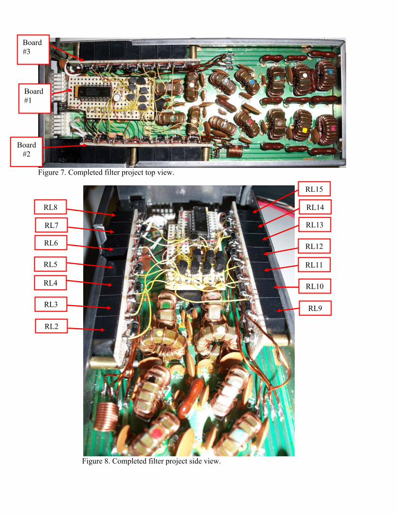
Figure 7. Completed filter project top view.
Figure 8. Completed filter project side view.
Board #1
Board #2
Board #3
RL8
RL7
RL6
RL5
RL4
RL3
RL2
RL15
RL14
RL13
RL12
RL11
RL10
RL9

8) Construct and install Board #1. This board is constructed on perf-board with 100 mil spacing. An IC socket is highly recommended. Refer to Figure 9 for reference. The 3 stiff metal pins holding up the board at points B,C and F are from wire wrap pins. An insulator is placed between the bottom of the board and the top of the existing circuitry below it. The other wires connecting to the PCB are 22AWG solid wire. Include sufficient length wires from the drain of each transistor to reach each relay. The test points in Figures 9 and 10 correspond to the test points in the schematic.
Figure 9. Board #1 (Control Board).
F 7 6 5 4 3 2 1C B
7.5V GND /RL
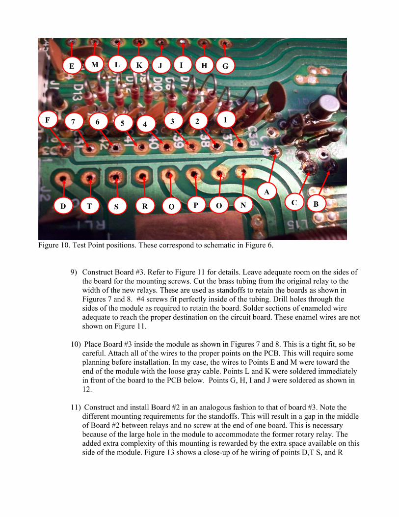
Figure 10. Test Point positions. These correspond to schematic in Figure 6.
9) Construct Board #3. Refer to Figure 11 for details. Leave adequate room on the sides of the board for the mounting screws. Cut the brass tubing from the original relay to the width of the new relays. These are used as standoffs to retain the boards as shown in Figures 7 and 8. #4 screws fit perfectly inside of the tubing. Drill holes through the sides of the module as required to retain the board. Solder sections of enameled wire adequate to reach the proper destination on the circuit board. These enamel wires are not shown on Figure 11.
10) Place Board #3 inside the module as shown in Figures 7 and 8. This is a tight fit, so be
careful. Attach all of the wires to the proper points on the PCB. This will require some planning before installation. In my case, the wires to Points E and M were toward the end of the module with the loose gray cable. Points L and K were soldered immediately in front of the board to the PCB below. Points G, H, I and J were soldered as shown in 12.
11) Construct and install Board #2 in an analogous fashion to that of board #3. Note the
different mounting requirements for the standoffs. This will result in a gap in the middle of Board #2 between relays and no screw at the end of one board. This is necessary because of the large hole in the module to accommodate the former rotary relay. The added extra complexity of this mounting is rewarded by the extra space available on this side of the module. Figure 13 shows a close-up of he wiring of points D,T S, and R
B C
F 7 6 5 4 3 2 1
D T S R Q P O N
A
E M L K J I H G
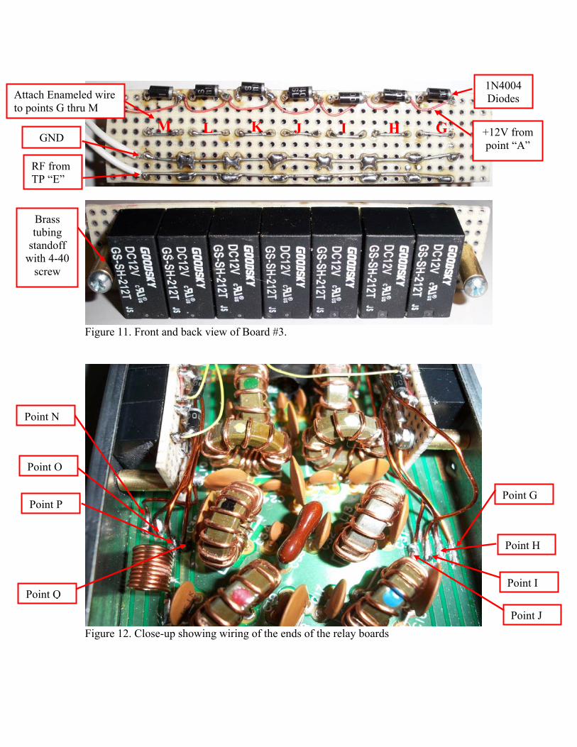
Figure 11. Front and back view of Board #3.
Figure 12. Close-up showing wiring of the ends of the relay boards
RF from TP “E”
GND M L G K J HI
Attach Enameled wire to points G thru M
1N4004 Diodes
+12V from point “A”
Brass tubing
standoff with 4-40
screw
Point G
Point H
Point I
Point J
Point N
Point O
Point P
Point Q
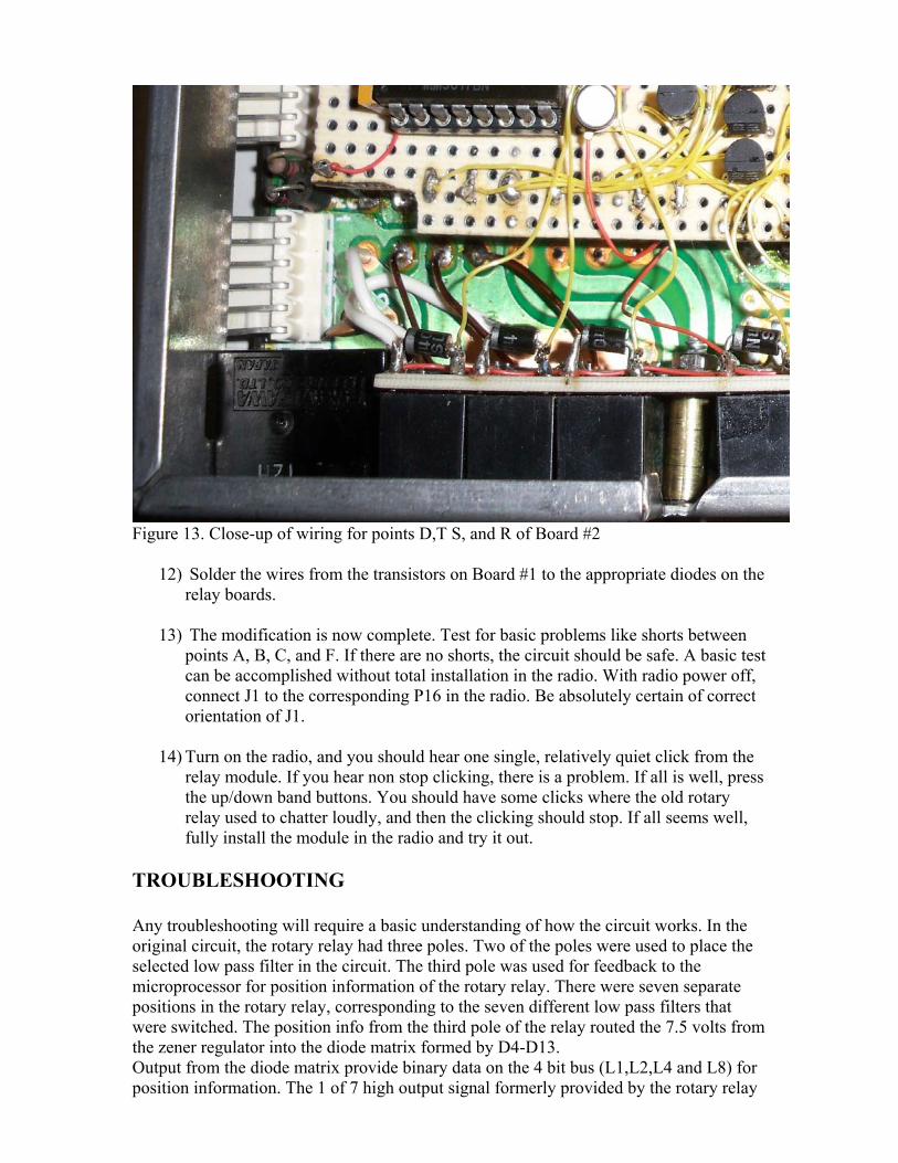
Figure 13. Close-up of wiring for points D,T S, and R of Board #2
12) Solder the wires from the transistors on Board #1 to the appropriate diodes on the relay boards.
13) The modification is now complete. Test for basic problems like shorts between
points A, B, C, and F. If there are no shorts, the circuit should be safe. A basic test can be accomplished without total installation in the radio. With radio power off, connect J1 to the corresponding P16 in the radio. Be absolutely certain of correct orientation of J1.
14) Turn on the radio, and you should hear one single, relatively quiet click from the
relay module. If you hear non stop clicking, there is a problem. If all is well, press the up/down band buttons. You should have some clicks where the old rotary relay used to chatter loudly, and then the clicking should stop. If all seems well, fully install the module in the radio and try it out.
TROUBLESHOOTING Any troubleshooting will require a basic understanding of how the circuit works. In the original circuit, the rotary relay had three poles. Two of the poles were used to place the selected low pass filter in the circuit. The third pole was used for feedback to the microprocessor for position information of the rotary relay. There were seven separate positions in the rotary relay, corresponding to the seven different low pass filters that were switched. The position info from the third pole of the relay routed the 7.5 volts from the zener regulator into the diode matrix formed by D4-D13. Output from the diode matrix provide binary data on the 4 bit bus (L1,L2,L4 and L8) for position information. The 1 of 7 high output signal formerly provided by the rotary relay
is now provided by the 4017 counter outputs. The pulse that formerly caused Q1 to advance the relay one position is now used to cause the counter to advance one count. The counter is decoded internally and 10 outputs provided. In this implementation, the 8th count is used to reset the counter so that it cycles back to output #1 being high. The single high output will remain high until a pulse advances the counter, at which time another output will go high. These outputs drive both the diode matrix and the gate of a MOSFET. A high signal on the MOSFET gate will turn it on and effectively ground one side of the connected relays. This performs the same function as the rotary relay without the noise, oxidation, and alignment issues. If the problem seems to be that the relays never stop chattering, that means the proper position information in not getting to the microprocessor. Verify that each output of the counter (Q0-Q6) has a high pulse, and that the pulse is reaching the diode matrix properly. If the symptoms are that you don’t hear any relay clicking, even when changing the bands, it is likely that there is a problem with the pulse getting to the counter. Verify the presence of a pulse at pin 14 of the 4017 while changing bands. If there is a pulse there, verify one of the outputs of the counter is high, and that the corresponding relays are being grounded. If they are being grounded, confirm 12V is present on the other side of the relay coil. If there is no pulse at pin 14 of the 4017 while changing bands, confirm he presence of a pulse at the “RL” pin of J1. If there is no pulse there, verify that it is there with the module disconnected from J1. If it is not there without the module connected, then the problem is outside the module. If it is there, the module is loading it down when connected. Assuming the pulse is at the “RL” pin of J1, the problem must be in the Q1 or Q2 circuitry. If the relays sound right when clicking, but there is low sensitivity in the receive and high collector current during transmit, either a relay is failing to key or some of the filter wiring is incorrect. Fortunately the low pass filters are DC shorts from input to output. The operation of the relays can be conducted with just J1 connected and the module out of the radio. For any given band, the proper connections can be tested for continuity between the “SWR1” pin of P1 and the “RA0” pin of J2. These points are clearly visible on the schematic on Figure 6. During proper operation, there should be low resistance continuity between those two pins. Referring the schematic on Figure 6 and using the 1.8 MHz low pass filter as an example, Pin 3 of the 4017 should be high. This should produce a high L1 on J1, with L2, L4, and L8 all low. The high level on pin 3 of the 4017 should also turn on Q3, which in turn should drive the coil of RL2 and RL9 low. This should key both RL2 and RLY 9, resulting in continuity between SWR1 and RA0. If there is not, going from left to right on the schematic, there should be continuity between SWR1 and the enameled wire on relay 9. Continuing, there should be continuity between SWR1 and points G and N. Continuing, there should be continuity between SWR1 and the enameled wire on RL9. If the continuity is not present, either the relay is not keying, or the wiring is going to an incorrect relay.

Figure 14. Schematic of original concept by F5IKI.
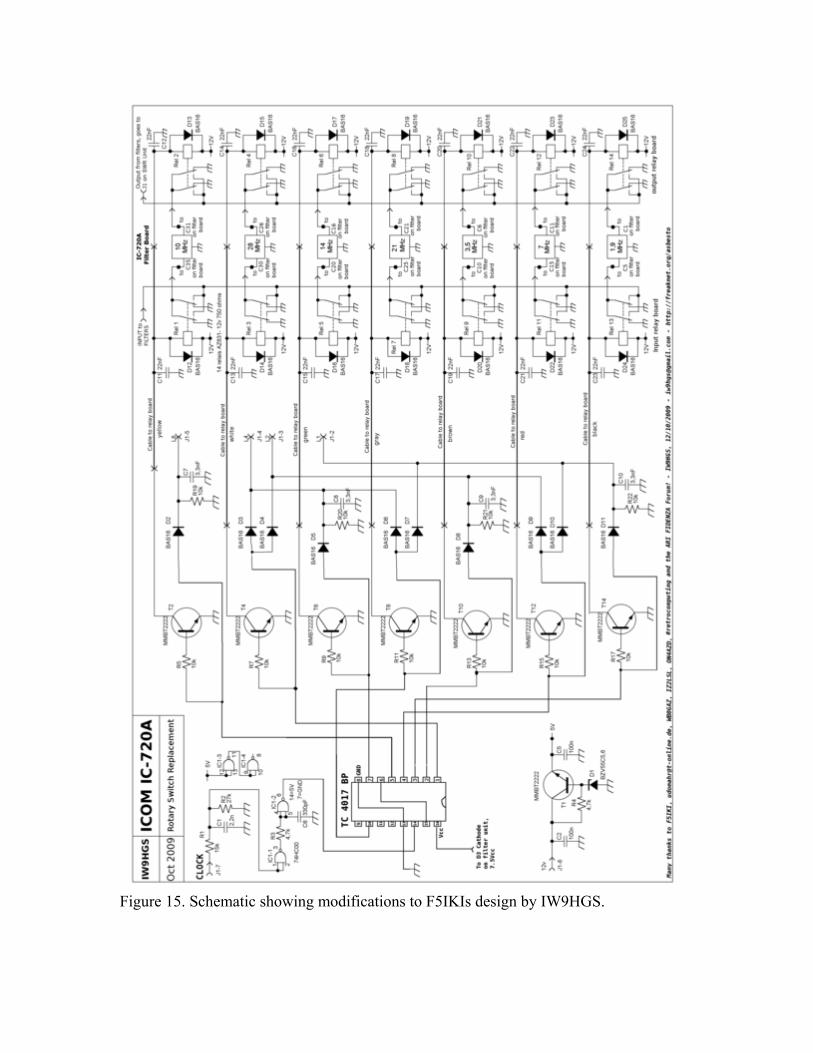
Figure 15. Schematic showing modifications to F5IKIs design by IW9HGS.