51
ICs for Communications Memory Time Switch Extended Large MTSXL PEB 2447 Version 1.2 Data Sheet 03.97 T2447-XV12-D2-7600

ICs for Communications
Memory Time Switch Extended LargeMTSXL
PEB 2447 Version 1.2
Data Sheet 03.97T2447-XV12-D2-7600
Edition 03.97This edition was realized using the software system FrameMaker.Published by Siemens AG,Bereich Halbleiter, Marketing-Kommunikation, Balanstraße 73,81541 München© Siemens AG 1997.All Rights Reserved.Attention please!As far as patents or other rights of third parties are concerned, liability is only assumed for components, not for applications, processes and circuits implemented within components or assemblies.The information describes the type of component and shall not be considered as assured characteristics.Terms of delivery and rights to change design reserved.For questions on technology, delivery and prices please contact the Semiconductor Group Offices in Germany or the Siemens Companies and Representatives worldwide (see address list).Due to technical requirements components may contain dangerous substances. For information on the types in question please contact your nearest Siemens Office, Semiconductor Group.Siemens AG is an approved CECC manufacturer.PackingPlease use the recycling operators known to you. We can also help you – get in touch with your nearest sales office. By agreement we will take packing material back, if it is sorted. You must bear the costs of transport. For packing material that is returned to us unsorted or which we are not obliged to accept, we shall have to invoice you for any costs incurred.Components used in life-support devices or systems must be expressly authorized for such purpose!Critical components1 of the Semiconductor Group of Siemens AG, may only be used in life-support devices or systems2 with the express written approval of the Semiconductor Group of Siemens AG.1 A critical component is a component used in a life-support device or system whose failure can reasonably be
expected to cause the failure of that life-support device or system, or to affect its safety or effectiveness of that device or system.
2 Life support devices or systems are intended (a) to be implanted in the human body, or (b) to support and/or maintain and sustain human life. If they fail, it is reasonable to assume that the health of the user may be en-dangered.
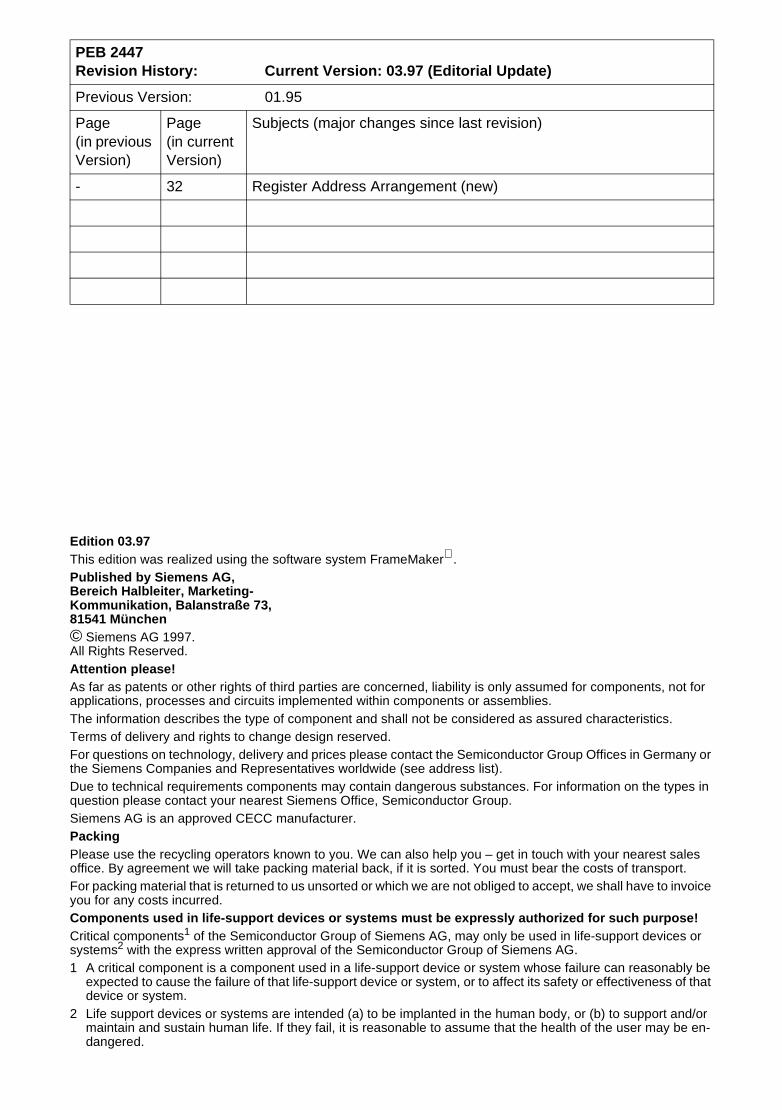
PEB 2447Revision History: Current Version: 03.97 (Editorial Update)
Previous Version: 01.95
Page(in previous Version)
Page(in current Version)
Subjects (major changes since last revision)
- 32 Register Address Arrangement (new)
PEB 2447
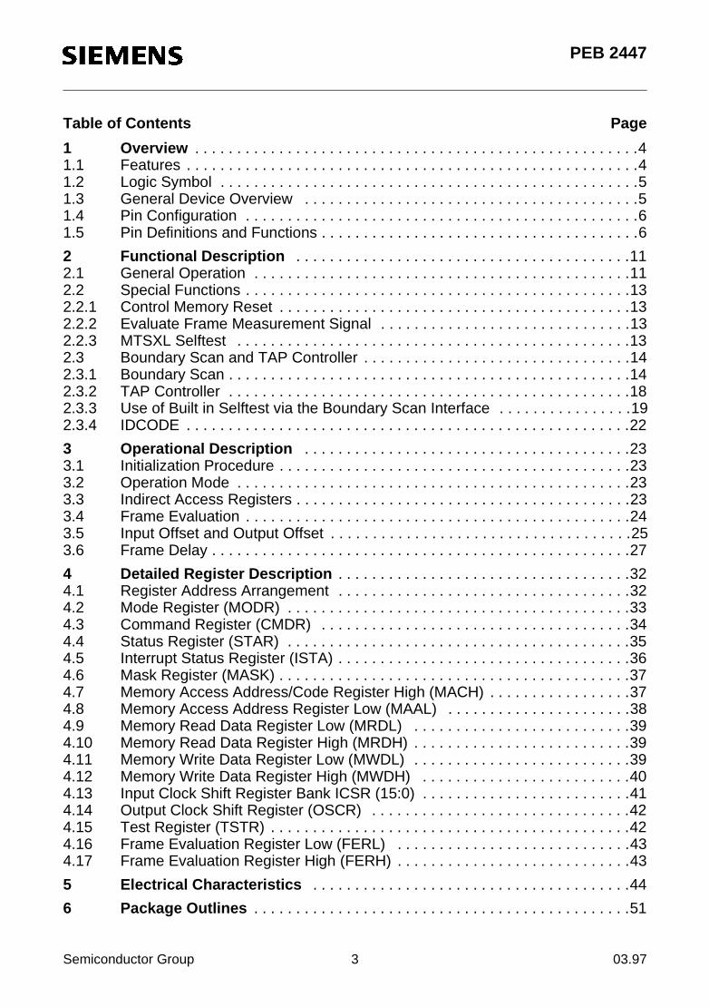
Table of Contents Page
Semiconductor Group 3 03.97
1 Overview . . . . . . . . . . . . . . . . . . . . . . . . . . . . . . . . . . . . . . . . . . . . . . . . . . . . .41.1 Features . . . . . . . . . . . . . . . . . . . . . . . . . . . . . . . . . . . . . . . . . . . . . . . . . . . . . .41.2 Logic Symbol . . . . . . . . . . . . . . . . . . . . . . . . . . . . . . . . . . . . . . . . . . . . . . . . . .51.3 General Device Overview . . . . . . . . . . . . . . . . . . . . . . . . . . . . . . . . . . . . . . . .51.4 Pin Configuration . . . . . . . . . . . . . . . . . . . . . . . . . . . . . . . . . . . . . . . . . . . . . . .61.5 Pin Definitions and Functions . . . . . . . . . . . . . . . . . . . . . . . . . . . . . . . . . . . . . .6
2 Functional Description . . . . . . . . . . . . . . . . . . . . . . . . . . . . . . . . . . . . . . . .112.1 General Operation . . . . . . . . . . . . . . . . . . . . . . . . . . . . . . . . . . . . . . . . . . . . .112.2 Special Functions . . . . . . . . . . . . . . . . . . . . . . . . . . . . . . . . . . . . . . . . . . . . . .132.2.1 Control Memory Reset . . . . . . . . . . . . . . . . . . . . . . . . . . . . . . . . . . . . . . . . . .132.2.2 Evaluate Frame Measurement Signal . . . . . . . . . . . . . . . . . . . . . . . . . . . . . .132.2.3 MTSXL Selftest . . . . . . . . . . . . . . . . . . . . . . . . . . . . . . . . . . . . . . . . . . . . . . .132.3 Boundary Scan and TAP Controller . . . . . . . . . . . . . . . . . . . . . . . . . . . . . . . .142.3.1 Boundary Scan . . . . . . . . . . . . . . . . . . . . . . . . . . . . . . . . . . . . . . . . . . . . . . . .142.3.2 TAP Controller . . . . . . . . . . . . . . . . . . . . . . . . . . . . . . . . . . . . . . . . . . . . . . . .182.3.3 Use of Built in Selftest via the Boundary Scan Interface . . . . . . . . . . . . . . . .192.3.4 IDCODE . . . . . . . . . . . . . . . . . . . . . . . . . . . . . . . . . . . . . . . . . . . . . . . . . . . . .22
3 Operational Description . . . . . . . . . . . . . . . . . . . . . . . . . . . . . . . . . . . . . . .233.1 Initialization Procedure . . . . . . . . . . . . . . . . . . . . . . . . . . . . . . . . . . . . . . . . . .233.2 Operation Mode . . . . . . . . . . . . . . . . . . . . . . . . . . . . . . . . . . . . . . . . . . . . . . .233.3 Indirect Access Registers . . . . . . . . . . . . . . . . . . . . . . . . . . . . . . . . . . . . . . . .233.4 Frame Evaluation . . . . . . . . . . . . . . . . . . . . . . . . . . . . . . . . . . . . . . . . . . . . . .243.5 Input Offset and Output Offset . . . . . . . . . . . . . . . . . . . . . . . . . . . . . . . . . . . .253.6 Frame Delay . . . . . . . . . . . . . . . . . . . . . . . . . . . . . . . . . . . . . . . . . . . . . . . . . .27
4 Detailed Register Description . . . . . . . . . . . . . . . . . . . . . . . . . . . . . . . . . . .324.1 Register Address Arrangement . . . . . . . . . . . . . . . . . . . . . . . . . . . . . . . . . . .324.2 Mode Register (MODR) . . . . . . . . . . . . . . . . . . . . . . . . . . . . . . . . . . . . . . . . .334.3 Command Register (CMDR) . . . . . . . . . . . . . . . . . . . . . . . . . . . . . . . . . . . . .344.4 Status Register (STAR) . . . . . . . . . . . . . . . . . . . . . . . . . . . . . . . . . . . . . . . . .354.5 Interrupt Status Register (ISTA) . . . . . . . . . . . . . . . . . . . . . . . . . . . . . . . . . . .364.6 Mask Register (MASK) . . . . . . . . . . . . . . . . . . . . . . . . . . . . . . . . . . . . . . . . . .374.7 Memory Access Address/Code Register High (MACH) . . . . . . . . . . . . . . . . .374.8 Memory Access Address Register Low (MAAL) . . . . . . . . . . . . . . . . . . . . . .384.9 Memory Read Data Register Low (MRDL) . . . . . . . . . . . . . . . . . . . . . . . . . .394.10 Memory Read Data Register High (MRDH) . . . . . . . . . . . . . . . . . . . . . . . . . .394.11 Memory Write Data Register Low (MWDL) . . . . . . . . . . . . . . . . . . . . . . . . . .394.12 Memory Write Data Register High (MWDH) . . . . . . . . . . . . . . . . . . . . . . . . .404.13 Input Clock Shift Register Bank ICSR (15:0) . . . . . . . . . . . . . . . . . . . . . . . . .414.14 Output Clock Shift Register (OSCR) . . . . . . . . . . . . . . . . . . . . . . . . . . . . . . .424.15 Test Register (TSTR) . . . . . . . . . . . . . . . . . . . . . . . . . . . . . . . . . . . . . . . . . . .424.16 Frame Evaluation Register Low (FERL) . . . . . . . . . . . . . . . . . . . . . . . . . . . .434.17 Frame Evaluation Register High (FERH) . . . . . . . . . . . . . . . . . . . . . . . . . . . .43
5 Electrical Characteristics . . . . . . . . . . . . . . . . . . . . . . . . . . . . . . . . . . . . . .44
6 Package Outlines . . . . . . . . . . . . . . . . . . . . . . . . . . . . . . . . . . . . . . . . . . . . .51

P-MQFP-100-2
Memory Time Switch Extended LargeMTSXL
PEB 2447
Version 1.2 CMOS IC
1 Overview1.1 Features
• Non blocking time/space switch for 4.096- or 8.192-Mbit/s PCM systems
• Device clock 16.384 MHz• Switching of up to 2048 incoming PCM channels to
up to 2048 outgoing PCM channels• 32 input and 32 output PCM lines• Tristate function for further expansion and tandem ope• µP read access to PCM data
ration
• Programmable clock shift with half clock step resolution for input and output• Individual line delay measurement for 6 additional inputs• Individual input offset programmable for 16 PCM inputs• Boundary scan (fully IEEE1149.1 compatible)• Built-in selftest (also usable via boundary scan interface)• 8-bit Intel type demultiplexed µP interface• All registers accessible by direct addressing• In-operation adjustment of bit sampling without bit errors• Low power consumption• Single 5 V power supply
Semiconductor Group 4 03.97
Type Ordering Code Package
PEB 2447 H Q67103-H6594 P-MQFP-100-2
PEB 2447
Overview
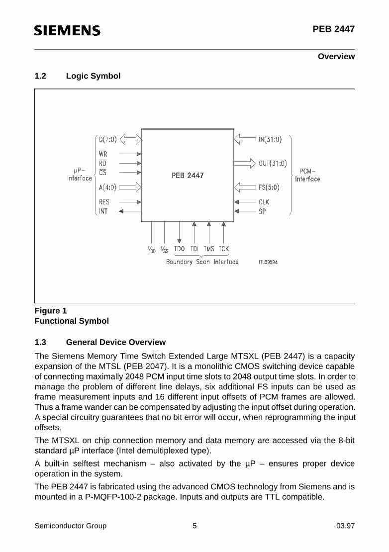
1.2 Logic Symbol
Figure 1Functional Symbol
1.3 General Device Overview
The Siemens Memory Time Switch Extended Large MTSXL (PEB 2447) is a capacityexpansion of the MTSL (PEB 2047). It is a monolithic CMOS switching device capableof connecting maximally 2048 PCM input time slots to 2048 output time slots. In order tomanage the problem of different line delays, six additional FS inputs can be used asframe measurement inputs and 16 different input offsets of PCM frames are allowed.Thus a frame wander can be compensated by adjusting the input offset during operation.A special circuitry guarantees that no bit error will occur, when reprogramming the inputoffsets.
The MTSXL on chip connection memory and data memory are accessed via the 8-bitstandard µP interface (Intel demultiplexed type).
A built-in selftest mechanism – also activated by the µP – ensures proper deviceoperation in the system.
The PEB 2447 is fabricated using the advanced CMOS technology from Siemens and ismounted in a P-MQFP-100-2 package. Inputs and outputs are TTL compatible.
Semiconductor Group 5 03.97

PEB 2447
Overview
1.4 Pin Configuration(top view)
Figure 2
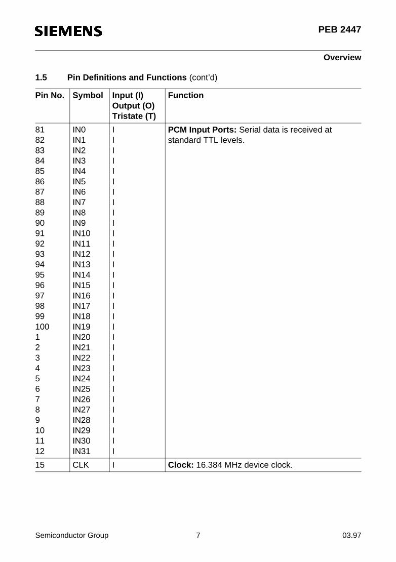
1.5 Pin Definitions and Functions
Pin No. Symbol Input (I)Output (O)Tristate (T)
Function
144167
VSS I Ground (0 V)
134066
VDD I Supply Voltage: 5 V + 5 %.
ITP09593
IN20
IN21
IN22
IN23
IN24
IN25
IN26
IN27
IN28
IN29
IN30
IN31
CLK
FS0
FS1
FS2
FS3
FS4
FS5 A4 A3 A2 A1 A0 CS RES
WR RD
1
80 79 78 77 76 75 74 73 72 71 70 69 68 67 66 65 64 63 62 61 60 59 58 57 56 55 54 53 52 51
2 3 4 5 6 7 8 9 10 11 12 13 14 15 16 17 18 19 20 21 22 23 24 25 26 27 28 29 30IN19 100
99IN1898IN1797IN1696IN1595IN1494IN1393IN1292IN1191IN1090IN989IN888IN787IN686IN585IN484IN383IN282IN181IN0
SP31D732D633D534D435D336D237D138D039
4041
OUT3142OUT3043OUT2944OUT2845OUT2746OUT2647OUT2548OUT2449
OUT
22
50
OUT
21O
UT20
OUT
19O
UT18
OUT
17O
UT16
OUT
15O
UT14
OUT
13O
UT12
OUT
11O
UT10
OUT
9O
UT8
OUT
7O
UT6
OUT
5O
UT4
OUT
3O
UT2
OUT
1O
UT0
INT
TDO
TMS
TDI
TCK
OUT23
DDVVSS
V DD V SS
IndexMarking
SSV V DD
PEB 2447
Semiconductor Group 6 03.97
PEB 2447
Overview
81828384858687888990919293949596979899100123456789101112
IN0IN1IN2IN3IN4IN5IN6IN7IN8IN9IN10IN11IN12IN13IN14IN15IN16IN17IN18IN19IN20IN21IN22IN23IN24IN25IN26IN27IN28IN29IN30IN31
IIIIIIIIIIIIIIIIIIIIIIIIIIIIIIII
PCM Input Ports: Serial data is received at standard TTL levels.
15 CLK I Clock: 16.384 MHz device clock.
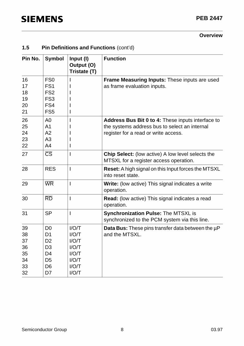
1.5 Pin Definitions and Functions (cont’d)
Pin No. Symbol Input (I)Output (O)Tristate (T)
Function
Semiconductor Group 7 03.97
PEB 2447
Overview
161718192021
FS0FS1FS2FS3FS4FS5
IIIIII
Frame Measuring Inputs: These inputs are used as frame evaluation inputs.
2625242322
A0A1A2A3A4
IIIII
Address Bus Bit 0 to 4: These inputs interface to the systems address bus to select an internal register for a read or write access.
27 CS I Chip Select: (low active) A low level selects the MTSXL for a register access operation.
28 RES I Reset: A high signal on this Input forces the MTSXL into reset state.
29 WR I Write: (low active) This signal indicates a write operation.
30 RD I Read: (low active) This signal indicates a read operation.
31 SP I Synchronization Pulse: The MTSXL is synchronized to the PCM system via this line.
3938373635343332
D0D1D2D3D4D5D6D7
I/O/TI/O/TI/O/TI/O/TI/O/TI/O/TI/O/TI/O/T
Data Bus: These pins transfer data between the µP and the MTSXL.
1.5 Pin Definitions and Functions (cont’d)
Pin No. Symbol Input (I)Output (O)Tristate (T)
Function
Semiconductor Group 8 03.97

PEB 2447
Overview
7574737271706968
OUT0OUT1OUT2OUT3OUT4OUT5OUT6OUT7
O/TO/TO/TO/TO/TO/TO/TO/T
PCM Output Port: Serial data is sent by these lines. These pins can be tristated.
656463626160595857565554535251504948474645444342
OUT8OUT9OUT10OUT11OUT12OUT13OUT14OUT15OUT16OUT17OUT18OUT19OUT20OUT21OUT22OUT23OUT24OUT25OUT26OUT27OUT28OUT29OUT30OUT31
O/TO/TO/TO/TO/TO/TO/TO/TO/TO/TO/TO/TO/TO/TO/TO/TO/TO/TO/TO/TO/TO/TO/TO/T
76 INT O(Open Drain)
Interrupt Line: Active low.Reset when reading ISTA
77 TDO O/T Test Data Output: In the appropriate TAP controller state test data, an instruction or the selftest result is shifted out via this line.
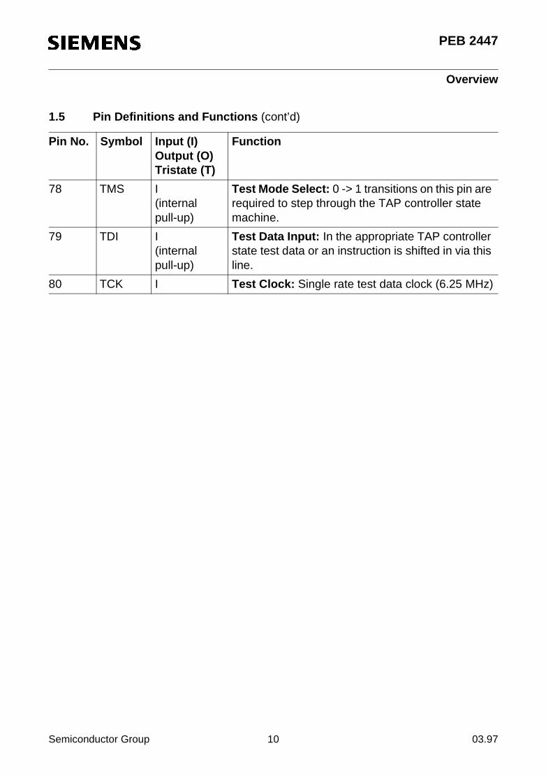
1.5 Pin Definitions and Functions (cont’d)
Pin No. Symbol Input (I)Output (O)Tristate (T)
Function
Semiconductor Group 9 03.97
PEB 2447
Overview
78 TMS I(internal pull-up)
Test Mode Select: 0 -> 1 transitions on this pin are required to step through the TAP controller state machine.
79 TDI I(internal pull-up)
Test Data Input: In the appropriate TAP controller state test data or an instruction is shifted in via this line.
80 TCK I Test Clock: Single rate test data clock (6.25 MHz)
1.5 Pin Definitions and Functions (cont’d)
Pin No. Symbol Input (I)Output (O)Tristate (T)
Function
Semiconductor Group 10 03.97
PEB 2447
Functional Description
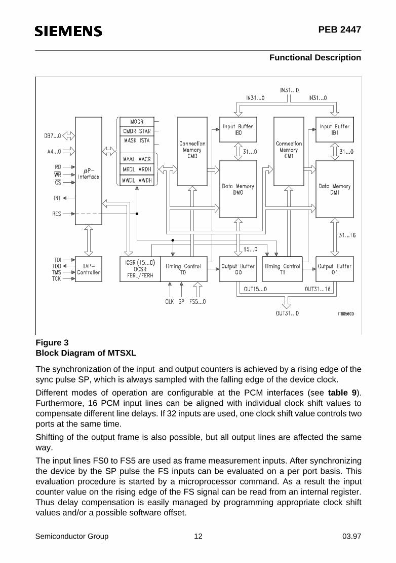
2 Functional Description
The MTSXL is a memory time switch device. Operating with a device clock of16.384 MHz it can connect any of 2048 PCM input channels to any of 2048 outputchannels.
A general block diagram of the MTSXL is shown in figure 3.
2.1 General Operation
The input information of a complete frame is stored twice in the two on-chip 16-kbit datamemories DM 0 and DM 1 (Data Memory 0 and Data Memory 1). The incoming2048 channels of 8 bits each are written in sequence into fixed positions of DM 0 andDM 1. This is controlled by the input counter in the timing control block with a 8 kHzrepetition rate.
For outputting, two connection memories (CM 0 and CM 1) are read in sequencesynchronously. Each entry in the connection memory CM 0 / CM 1 points to a locationin data memory DM 0 / DM 1. The byte in this data memory location is transferred intothe current output time slot. The read access to the CM’s is controlled by an outputcounter. CM 0 supplies the PCM data for outputs OUT0 to OUT15, CM 1 supplies thePCM data for outputs OUT16 to OUT31.
Semiconductor Group 11 03.97
PEB 2447
Functional Description
Figure 3Block Diagram of MTSXL
The synchronization of the input and output counters is achieved by a rising edge of thesync pulse SP, which is always sampled with the falling edge of the device clock.
Different modes of operation are configurable at the PCM interfaces (see table 9).Furthermore, 16 PCM input lines can be aligned with individual clock shift values tocompensate different line delays. If 32 inputs are used, one clock shift value controls twoports at the same time.
Shifting of the output frame is also possible, but all output lines are affected the sameway.
The input lines FS0 to FS5 are used as frame measurement inputs. After synchronizingthe device by the SP pulse the FS inputs can be evaluated on a per port basis. Thisevaluation procedure is started by a microprocessor command. As a result the inputcounter value on the rising edge of the FS signal can be read from an internal register.Thus delay compensation is easily managed by programming appropriate clock shiftvalues and/or a possible software offset.
Semiconductor Group 12 03.97

PEB 2447
Functional Description
During operation of the chip a frame length check is also supplied, which controls correctsynchronization by the SP pulse and generates an interrupt in case of lost or achievedsynchronization.
The unused output ports are tristated by mode selection, whereas unused time slots aretristated by an additional bit in the control memory. By using this tristate capability theMTSXL can be easily expanded to a time switch of any size.
The standard 8-bit µP interface can communicate with Intel demultiplexedmicroprocessors. It gives access to the internal registers and to the control and datamemory. All registers are directly addressable. The memories are accessed by a simplefour byte indirect access method.
2.2 Special Functions
The activity of all special functions can be read in the status register. Completion of thesefunctions is indicated by interrupts.
2.2.1 Control Memory Reset
Initialization of the device after a hardware reset (RES) is easily done with a µPcommand “control memory reset”. After finishing this procedure all control memorychannels contain the information “tristated”. Apart from this tristate information thecontents of the C Memory is undefined.
2.2.2 Evaluate Frame Measurement Signal
A command including the address (0 … 5) will be given by the µP. The rising edge of thecorresponding frame measurement signal (FS0 … FS5) will be evaluated. The exacttiming of the FS edge can then be read from an internal 12-bit register (resolution of acomplete 8 kHz frame in half 16 MHz clock periods).
2.2.3 MTSXL Selftest
The switching path of the MTSXL including input buffer, data memory, control memory,output buffer and timing control can be tested in the system by a 2-step built-in selftest.Activating this mechanism takes 2 × 0.625 ms (16.384 MHz). Finally the result “selftestok/selftest not ok” can be read from the internal status register.
After test completion the control memory has also been reset (contains the informationtristated).
The selftest can also be started and checked via the boundary scan interface.
Note: For correct execution of the built-in selftest the MTSXL needs a value ofICSR = 00. If MODR:PSB = 0 (e.g. after hardware reset) this value is programmedautomatically after start of the selftest procedure. If ICSR does not contain “00”with MODR:PSB = 1 the selftest will fail.
Semiconductor Group 13 03.97
PEB 2447
Functional Description
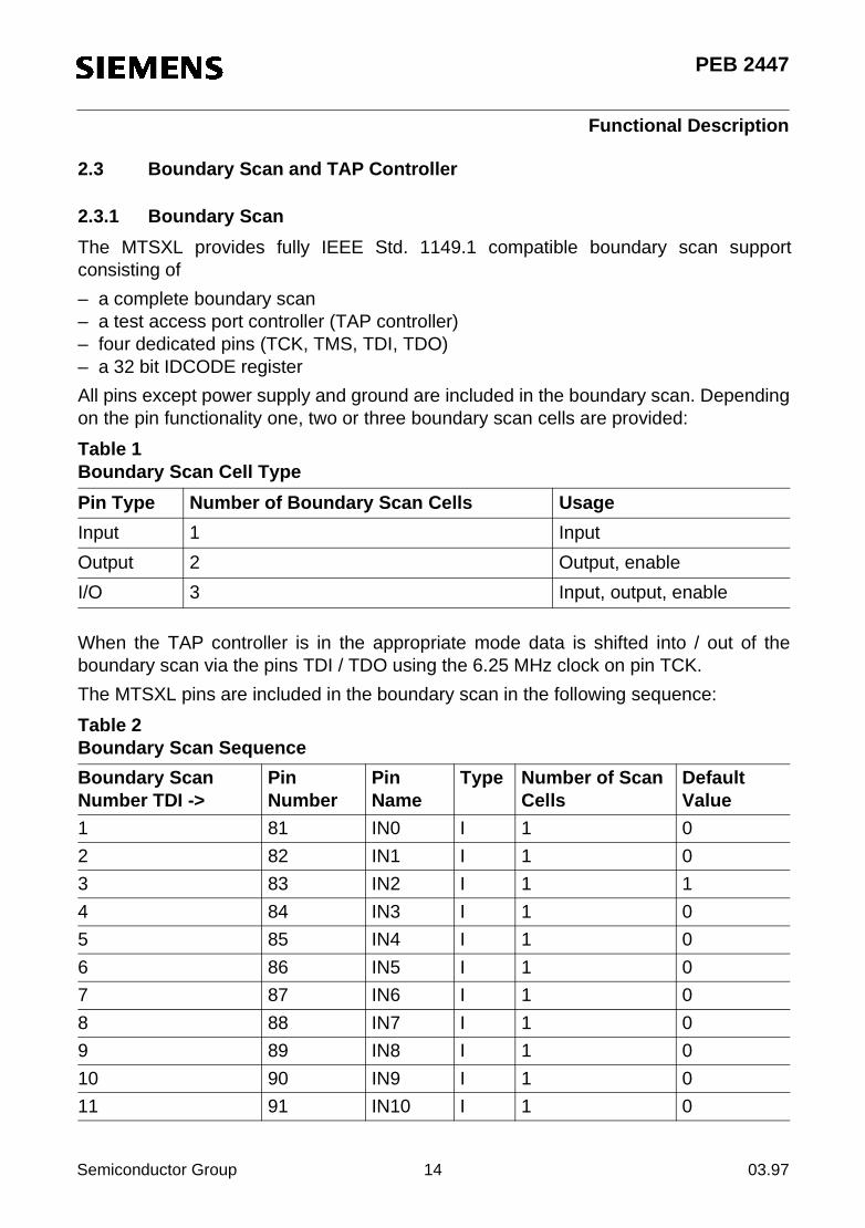
2.3 Boundary Scan and TAP Controller
2.3.1 Boundary Scan
The MTSXL provides fully IEEE Std. 1149.1 compatible boundary scan supportconsisting of
– a complete boundary scan– a test access port controller (TAP controller)– four dedicated pins (TCK, TMS, TDI, TDO)– a 32 bit IDCODE register
All pins except power supply and ground are included in the boundary scan. Dependingon the pin functionality one, two or three boundary scan cells are provided:
When the TAP controller is in the appropriate mode data is shifted into / out of theboundary scan via the pins TDI / TDO using the 6.25 MHz clock on pin TCK.
The MTSXL pins are included in the boundary scan in the following sequence:
Table 1Boundary Scan Cell Type
Pin Type Number of Boundary Scan Cells Usage
Input 1 Input
Output 2 Output, enable
I/O 3 Input, output, enable
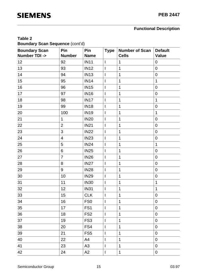
Table 2Boundary Scan Sequence
Boundary Scan Number TDI ->
Pin Number
Pin Name
Type Number of Scan Cells
Default Value
1 81 IN0 I 1 0
2 82 IN1 I 1 0
3 83 IN2 I 1 1
4 84 IN3 I 1 0
5 85 IN4 I 1 0
6 86 IN5 I 1 0
7 87 IN6 I 1 0
8 88 IN7 I 1 0
9 89 IN8 I 1 0
10 90 IN9 I 1 0
11 91 IN10 I 1 0
Semiconductor Group 14 03.97
PEB 2447
Functional Description
12 92 IN11 I 1 0
13 93 IN12 I 1 0
14 94 IN13 I 1 0
15 95 IN14 I 1 1
16 96 IN15 I 1 0
17 97 IN16 I 1 0
18 98 IN17 I 1 1
19 99 IN18 I 1 0
20 100 IN19 I 1 1
21 1 IN20 I 1 0
22 2 IN21 I 1 0
23 3 IN22 I 1 0
24 4 IN23 I 1 0
25 5 IN24 I 1 1
26 6 IN25 I 1 0
27 7 IN26 I 1 0
28 8 IN27 I 1 0
29 9 IN28 I 1 0
30 10 IN29 I 1 0
31 11 IN30 I 1 1
32 12 IN31 I 1 1
33 15 CLK I 1 0
34 16 FS0 I 1 0
35 17 FS1 I 1 0
36 18 FS2 I 1 0
37 19 FS3 I 1 0
38 20 FS4 I 1 0
39 21 FS5 I 1 0
40 22 A4 I 1 0
41 23 A3 I 1 0
42 24 A2 I 1 0
Table 2Boundary Scan Sequence (cont’d)
Boundary Scan Number TDI ->
Pin Number
Pin Name
Type Number of Scan Cells
Default Value
Semiconductor Group 15 03.97

PEB 2447
Functional Description
43 25 A1 I 1 0
44 26 A0 I 1 0
45 27 CS I 1 0
46 28 RES I 1 0
47 29 WR I 1 0
48 30 RD I 1 0
49 31 SP I 1 0
50 32 AD7 IO 3 000
51 33 AD6 IO 3 000
52 34 AD5 IO 3 000
53 35 AD4 IO 3 000
54 36 AD3 IO 3 000
55 37 AD2 IO 3 000
56 38 AD1 IO 3 000
57 39 AD0 IO 3 000
58 42 OUT31 O 2 00
59 43 OUT30 O 2 00
60 44 OUT29 O 2 00
61 45 OUT28 O 2 00
62 46 OUT27 O 2 00
63 47 OUT26 O 2 00
64 48 OUT25 O 2 00
65 49 OUT24 O 2 00
66 50 OUT23 O 2 00
67 51 OUT22 O 2 00
68 52 OUT21 O 2 00
69 53 OUT20 O 2 00
70 54 OUT19 O 2 00
71 55 OUT18 O 2 00
72 56 OUT17 O 2 00
73 57 OUT16 O 2 00
Table 2Boundary Scan Sequence (cont’d)
Boundary Scan Number TDI ->
Pin Number
Pin Name
Type Number of Scan Cells
Default Value
Semiconductor Group 16 03.97

PEB 2447
Functional Description
74 58 OUT15 O 2 00
75 59 OUT14 O 2 00
76 60 OUT13 O 2 00
77 61 OUT12 O 2 00
78 62 OUT11 O 2 00
79 63 OUT10 O 2 00
80 64 OUT9 O 2 00
81 65 OUT8 O 2 00
82 68 OUT7 O 2 00
83 69 OUT6 O 2 00
84 70 OUT5 O 2 00
85 71 OUT4 O 2 00
86 72 OUT3 O 2 00
87 73 OUT2 O 2 00
88 74 OUT1 O 2 00
89 75 OUT0 O 2 00
90 76 INT O 2 00
Table 2Boundary Scan Sequence (cont’d)
Boundary Scan Number TDI ->
Pin Number
Pin Name
Type Number of Scan Cells
Default Value
Semiconductor Group 17 03.97

PEB 2447
Functional Description
2.3.2 TAP Controller
The TAP controller implements a state machine defined in the JTAG standardIEEE1149.1. The instruction register of the controller is extended to 4 bits in order toincrease the number of instructions. This is necessary for the use of the build in selftestprocedure via the boundary scan interface:
The standard instructions are implemented according to the JTAG standard, just theinstruction register is extended to 4 bits. At the new instructions TAP_TEST1.. 8 specialinternal test signals are activated during the state “RUN TEST / IDLE”.
The MTSXL only uses TAP_TEST1 and TAP_TEST2 according to table 3.
Table 3Instruction Code of 4 Bit TAP Controller
Instruction Code
EXTEST 0000
INTEST 0001
SAMPLE / PRELOAD 0010
IDCODE 0011
BYPASS 11xx
TAP_TEST1: Start built in self test
0100
TAP_TEST2:Write selftest control register
0101
TAP_TEST3 0110
TAP_TEST4 0111
TAP_TEST5 1000
TAP_TEST6 1001
TAP_TEST7 1010
TAP_TEST8 1011
Semiconductor Group 18 03.97
PEB 2447
Functional Description
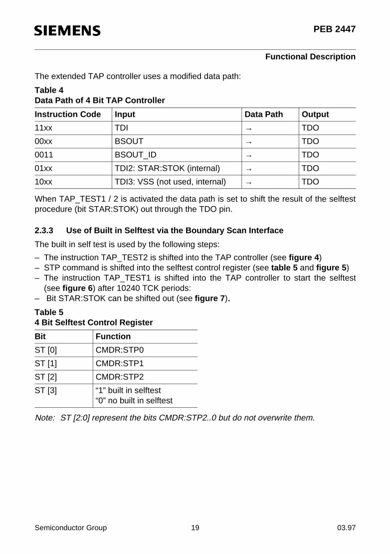
The extended TAP controller uses a modified data path:
When TAP_TEST1 / 2 is activated the data path is set to shift the result of the selftestprocedure (bit STAR:STOK) out through the TDO pin.
2.3.3 Use of Built in Selftest via the Boundary Scan Interface
The built in self test is used by the following steps:
– The instruction TAP_TEST2 is shifted into the TAP controller (see figure 4)– STP command is shifted into the selftest control register (see table 5 and figure 5)– The instruction TAP_TEST1 is shifted into the TAP controller to start the selftest
(see figure 6) after 10240 TCK periods:– Bit STAR:STOK can be shifted out (see figure 7).
Note: ST [2:0] represent the bits CMDR:STP2..0 but do not overwrite them.
Table 4Data Path of 4 Bit TAP Controller
Instruction Code Input Data Path Output
11xx TDI → TDO
00xx BSOUT → TDO
0011 BSOUT_ID → TDO
01xx TDI2: STAR:STOK (internal) → TDO
10xx TDI3: VSS (not used, internal) → TDO
Table 54 Bit Selftest Control Register
Bit Function
ST [0] CMDR:STP0
ST [1] CMDR:STP1
ST [2] CMDR:STP2
ST [3] “1” built in selftest“0” no built in selftest
Semiconductor Group 19 03.97

PEB 2447
Functional Description
The TAP controller state machine passes through the different states according tofigures 4 to 7.
Note: The state coding is only described for explanation purposes, it is externally notvisible.
Table 6States of TAP Controller (explanation for figures 4 to 7)
Controller State State Code
Exit2-DR 0
Exit1-DR 1
Shift-DR 2
Pause-DR 3
Select-IR-Scan 4
Update-DR 5
Capture-DR 6
Select-DR-Scan 7
Exit2-IR 8
Exit1-IR 9
Shift-IR A
Pause-IR B
Run-Test / Idle C
Update-IR D
Capture-IR E
Test-Logic-Reset F
Semiconductor Group 20 03.97

PEB 2447
Functional Description
Figure 4Starting Instruction “TAP_TEST2” (code 0101)
Figure 5Writing Selftest Control Register
Semiconductor Group 21 03.97

PEB 2447
Functional Description
Figure 6Start of Built in Selftest (instruction TAP_TEST1, code 0100)
Figure 7Readout of Selftest Result (after 10240 TCK periods)
Note: After the use of the selftest procedure over the µP Interface or the boundary scaninterface a hardware reset is necessary before the selftest procedure can bestarted again over the other interface.
2.3.4 IDCODE
The manufacturer code for MTSXL is according to table 2:
V1.2: 0010 0000 0000 0010 0101 0000 1000 001 1
Semiconductor Group 22 03.97
PEB 2447
Operational Description
3 Operational Description
3.1 Initialization Procedure
For a proper initialization of the MTSXL the following procedure is recommended:
First a reset pulse (RES) of at least two CLK clock periods has to be applied. All registerscontain now their reset values. In the next step the connection memories CM0/1 areinitialized by the commands CMDR:STP (1:0) = 01 (CM reset) or CMDR:STP(2:0) = 011 / 111 (MTSXL selftest).
After having programmed a CM reset command, it takes 4096 clock periods until alltristate control entries in the CM contain the value “1” (tristated).
If a selftest command was given, it takes 10 240 clock periods to achieve the sameeffect. Furthermore the register bit STAR:STOK (selftest o.k.) should read “1” in thiscase, in order to prove that there is no fault on the chip. The selftest command must begiven twice: the upper half of data memory (DM0, DM1) is tested when settingCMDR:STP (2:1) = 01, the lower half of DM0, DM1 is tested by setting CMDR:STP(2:1) = 11 (see table 10).
The activity of the procedures can be monitored in STAR:PACT and an interrupt willindicate their completion.
In all cases it is important, that the outputs are tristated by MODR:PSB = 0.
3.2 Operation Mode
The operation mode of the device is fixed by programming MODR:MD (1:0) (seetable 9).
3.3 Indirect Access Registers
The connection memories and data memories are accessible through the indirect accessregisters MACH, MAAL, MRDH, MRDL, MWDH and MWDL. An indirect access isactually started by writing register MACH (Memory Access Address/Code RegisterHigh). The code value inherent in this register defines, what action has to be performed.The low byte of the complete access address must be programmed to MAAL (MemoryAccess Address Register Low) before writing to MACH. If data are necessary to performthe access (e.g. in write operations), they have to be entered into MWDH (Memory WriteData Register High) and MWDL (Memory Write Data Register Low) before. In readaccesses the corresponding registers MRDH (Memory Read Data Register High) andMRDL (Memory Read Data Register Low) contain the required information after theinternal read process is completed.
Semiconductor Group 23 03.97
PEB 2447
Operational Description
Typical Write Operation: Typical Read Operation:
WR MWDL WR MAAL
WR MWDH WR MACH
WR MAAL RD STAR; STAR:MAC = 0
WR MACH RD MRDL
RD STAR; STAR:MAC = 0 RD MRDH
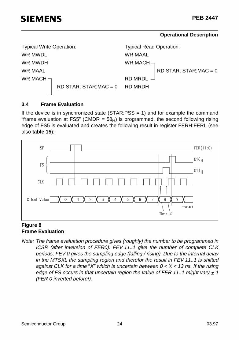
3.4 Frame Evaluation
If the device is in synchronized state (STAR:PSS = 1) and for example the command“frame evaluation at FS5” (CMDR = 58H) is programmed, the second following risingedge of FS5 is evaluated and creates the following result in register FERH:FERL (seealso table 15):
Figure 8Frame Evaluation
Note: The frame evaluation procedure gives (roughly) the number to be programmed inICSR (after inversion of FER0): FEV 11..1 give the number of complete CLKperiods; FEV 0 gives the sampling edge (falling / rising). Due to the internal delayin the MTSXL the sampling region and therefor the result in FEV 11..1 is shiftedagainst CLK for a time “X” which is uncertain between 0 < X < 13 ns. If the risingedge of FS occurs in that uncertain region the value of FER 11..1 might vary + 1(FER 0 inverted before!).
Semiconductor Group 24 03.97

PEB 2447
Operational Description
3.5 Input Offset and Output Offset
Based on the results of the frame evaluation procedures the input offsets can beadjusted by programming ICSR 7..0 corresponding to inputs IN 7..0. If dataoversampling is used, the values of ICSR 7..0 can be adjusted within some limits duringoperation without producing bit errors:
– clockrate = 2 × dataratepossible adjustment is one half clock period forward or backward.
– clockrate = 4 × dataratepossible adjustment is one clock period backward or two clock periods forward.
Figure 9Input Timing
Semiconductor Group 25 03.97
PEB 2447
Operational Description
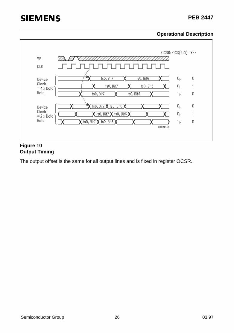
Figure 10Output Timing
The output offset is the same for all output lines and is fixed in register OCSR.
Semiconductor Group 26 03.97
PEB 2447
Operational Description
3.6 Frame Delay
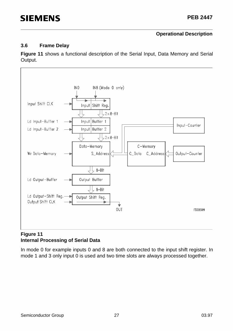
Figure 11 shows a functional description of the Serial Input, Data Memory and SerialOutput.
Figure 11Internal Processing of Serial Data
In mode 0 for example inputs 0 and 8 are both connected to the input shift register. Inmode 1 and 3 only input 0 is used and two time slots are always processed together.
Semiconductor Group 27 03.97

PEB 2447
Operational Description
Figure 12Internal Control Signals Mode 0 (OCSR = 0)
Note: O_SYN is a control signal for the synchronization of RD and WR access to thedata memory and not important for the external functionality. O_SYN frequency isfCLK / 2.
This figure shows that the inputs IN0 .. IN15 are written into the data memory at the sametime whereas IN16 .. IN31 are written one O_SYN period (= 2 CLK periods) later. Thevalue of ICSR 0..15 shifts the sampling points and the signal “Ld Inp Buffer 1” later intime (rightwards), the signals “Ld Inp Buffer 2” and “Wr S Memory” remain constant. Inthis example with OCSR = 0 the lower Inputs IN0 .. IN15 are written into data memorybefore Out15 (and Out31) is read.
With OCSR > 0 all Output Signals (Ld Outp Buffer and following) including the data(OUT0..15) on the internal data transfer bus is shifted earlier in time (leftwards). Thereforthe data is read out of the data memory earlier.
Due to the internal timing the frame delay is depending on the programmed input / outputtime slots and OCSR. The internal delay (number of time slots) can be deduced fromfigure 12 and is shown in table 7.
Semiconductor Group 28 03.97

PEB 2447
Operational Description
If the offset of output time slot to input time slot is greater or equal to the internal delaydue to table 7 the transmission of data is within the same frame (frame delay 0).
If the offset is smaller or even negative the transmission is in the next frame (framedelay 1).
Frame delay 1 also occurs when the programmed connection overrides the frame end(TS63 in Mode 0).
If the offset is smaller and overrides the frame end at the same time the frame delay is 2.
Examples: Connection IN1 ts1 -> OUT1 ts 5 (Offset 4ts) : frame delay 0
(OCSR=0) IN1 ts1 -> OUT1 ts 3 (Offset 2ts) : frame delay 1
IN1 ts62 -> OUT31 ts 0 (Offset 2ts) : frame delay 1
IN1 ts62 -> OUT1 ts 1 (Offset 3ts) : frame delay 2
Table 7Time Slots Delay Mode 0
OCS(4:0) IN Outputs
016
117
218
319
420
521
622
723
824
925
1026
1127
1228
1329
1430
1531
0 0 - 15 3 3 3 3 3 3 3 3 3 3 3 3 3 3 3 2
16 - 31 3 3 3 3 3 3 3 3 3 3 3 3 3 3 3 3
1 0 - 15 3 3 3 3 3 3 3 3 3 3 3 3 3 3 3 3
16 - 31 4 3 3 3 3 3 3 3 3 3 3 3 3 3 3 3
2 0 - 15 4 3 3 3 3 3 3 3 3 3 3 3 3 3 3 3
16 - 31 4 4 3 3 3 3 3 3 3 3 3 3 3 3 3 3
3 0 - 15 4 4 3 3 3 3 3 3 3 3 3 3 3 3 3 3
16 - 31 4 4 4 3 3 3 3 3 3 3 3 3 3 3 3 3
.
. Maximum delay 4 time slots
Semiconductor Group 29 03.97
PEB 2447
Operational Description
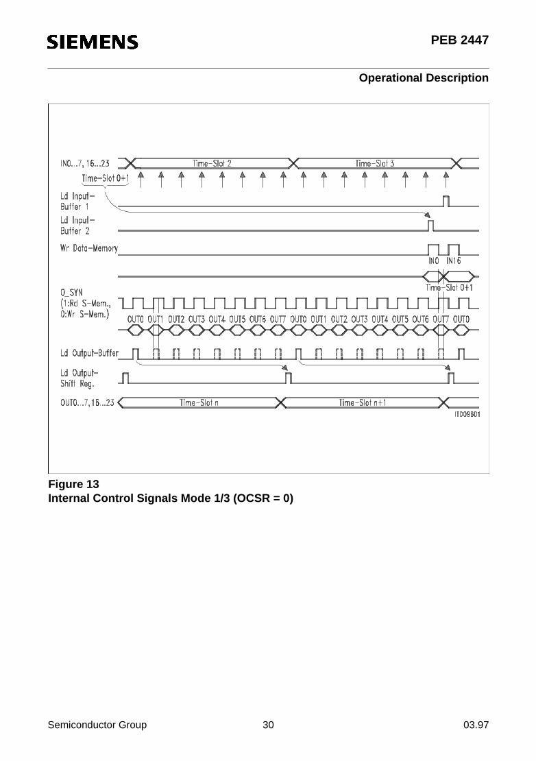
Figure 13Internal Control Signals Mode 1/3 (OCSR = 0)
Semiconductor Group 30 03.97
PEB 2447
Operational Description
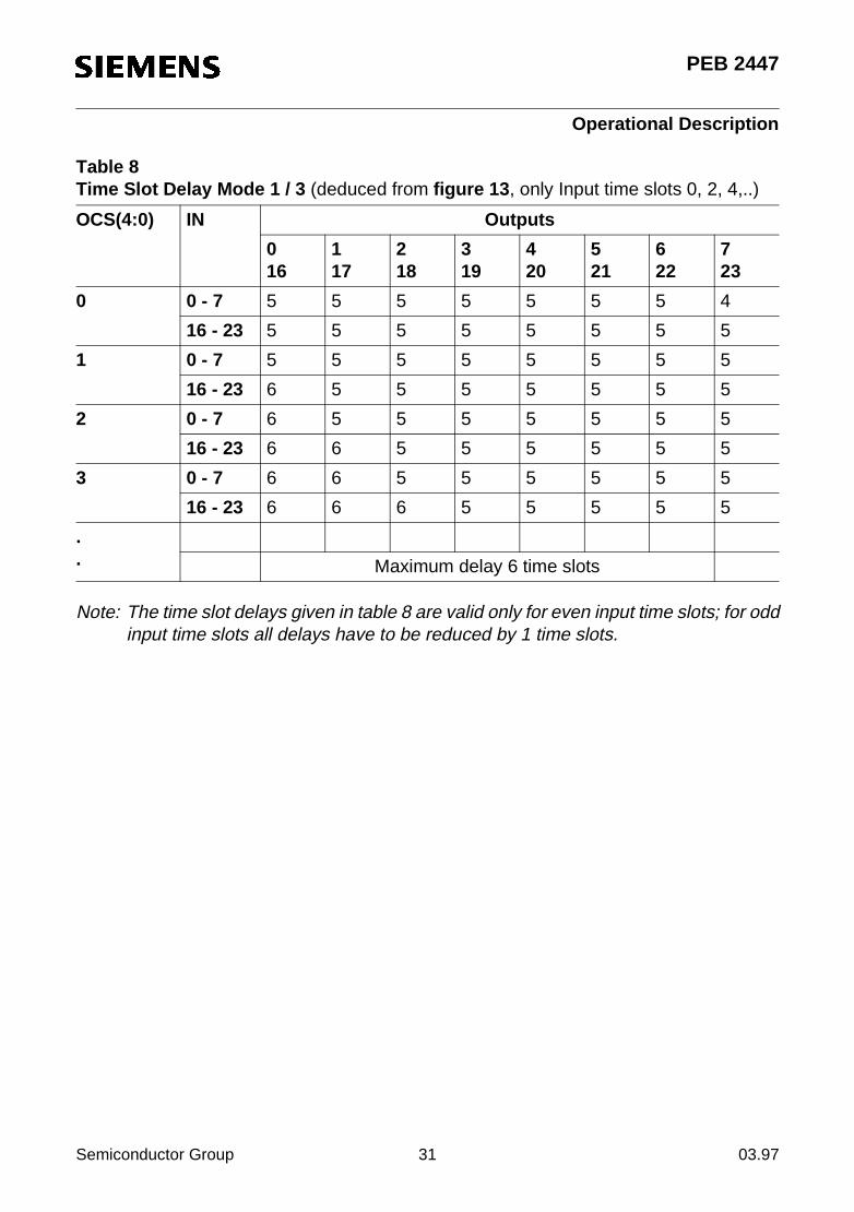
Note: The time slot delays given in table 8 are valid only for even input time slots; for oddinput time slots all delays have to be reduced by 1 time slots.
Table 8Time Slot Delay Mode 1 / 3 (deduced from figure 13, only Input time slots 0, 2, 4,..)
OCS(4:0) IN Outputs
016
117
218
319
420
521
622
723
0 0 - 7 5 5 5 5 5 5 5 4
16 - 23 5 5 5 5 5 5 5 5
1 0 - 7 5 5 5 5 5 5 5 5
16 - 23 6 5 5 5 5 5 5 5
2 0 - 7 6 5 5 5 5 5 5 5
16 - 23 6 6 5 5 5 5 5 5
3 0 - 7 6 6 5 5 5 5 5 5
16 - 23 6 6 6 5 5 5 5 5
.
. Maximum delay 6 time slots
Semiconductor Group 31 03.97
PEB 2447
Detailed Register Description
4 Detailed Register Description
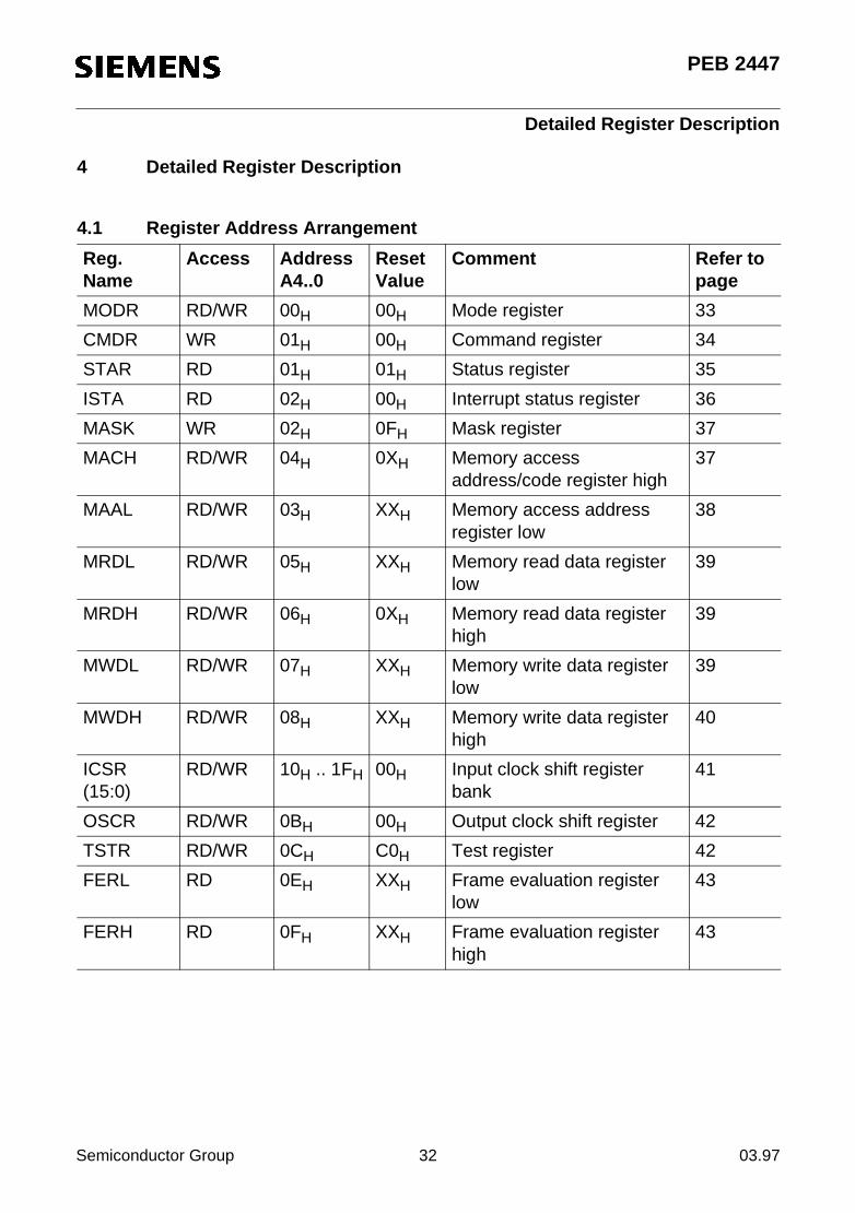
4.1 Register Address Arrangement
Reg. Name
Access AddressA4..0
Reset Value
Comment Refer to page
MODR RD/WR 00H 00H Mode register 33
CMDR WR 01H 00H Command register 34
STAR RD 01H 01H Status register 35
ISTA RD 02H 00H Interrupt status register 36
MASK WR 02H 0FH Mask register 37
MACH RD/WR 04H 0XH Memory access address/code register high
37
MAAL RD/WR 03H XXH Memory access address register low
38
MRDL RD/WR 05H XXH Memory read data register low
39
MRDH RD/WR 06H 0XH Memory read data register high
39
MWDL RD/WR 07H XXH Memory write data register low
39
MWDH RD/WR 08H XXH Memory write data register high
40
ICSR (15:0)
RD/WR 10H .. 1FH 00H Input clock shift register bank
41
OSCR RD/WR 0BH 00H Output clock shift register 42
TSTR RD/WR 0CH C0H Test register 42
FERL RD 0EH XXH Frame evaluation register low
43
FERH RD 0FH XXH Frame evaluation register high
43
Semiconductor Group 32 03.97

PEB 2447
Detailed Register Description
4.2 Mode Register (MODR)
Access in demultiplexed µP-interface mode:
Read/write, address: 00HReset value: 00H
PSB PCM Stand By; a logical 0 switches the PCM interface outputs to high impedance.
MD1 … MD0 Mode ; these bits define the chip operation mode according to the following table:
Note: *) In mode 3 the PCM lines OUT(n+16) drive the inverted values of lines OUT(n)or are tristated, if the corresponding PCM line is tristated.
Bit 7 Bit 0
PSB 0 0 0 0 0 MD1 MD0
Table 9Operation Modes
Operation Mode
Mode Bits MD1 MD0
Input # of Ports
Input Data Rate [MHz]
Output # of Ports
Output Data Rate [MHz]
Mode 0 0 0 32 4.096 32 4.096
Mode 1 0 1 16 8.192 16 8.192
Mode 3 1 1 16 8.192 1616*)
8.1928.192
Semiconductor Group 33 03.97
PEB 2447
Detailed Register Description
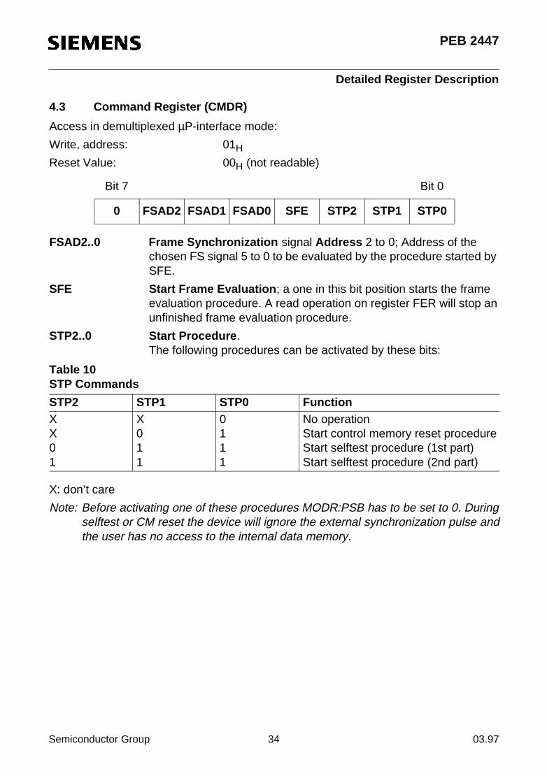
4.3 Command Register (CMDR)
Access in demultiplexed µP-interface mode:
Write, address: 01H
Reset Value: 00H (not readable)
FSAD2..0 Frame Synchronization signal Address 2 to 0; Address of the chosen FS signal 5 to 0 to be evaluated by the procedure started by SFE.
SFE Start Frame Evaluation; a one in this bit position starts the frame evaluation procedure. A read operation on register FER will stop an unfinished frame evaluation procedure.
STP2..0 Start Procedure.The following procedures can be activated by these bits:
X: don’t care
Note: Before activating one of these procedures MODR:PSB has to be set to 0. Duringselftest or CM reset the device will ignore the external synchronization pulse andthe user has no access to the internal data memory.
Bit 7 Bit 0
0 FSAD2 FSAD1 FSAD0 SFE STP2 STP1 STP0
Table 10STP Commands
STP2 STP1 STP0 FunctionXX01
X011
0111
No operationStart control memory reset procedureStart selftest procedure (1st part)Start selftest procedure (2nd part)
Semiconductor Group 34 03.97
PEB 2447
Detailed Register Description
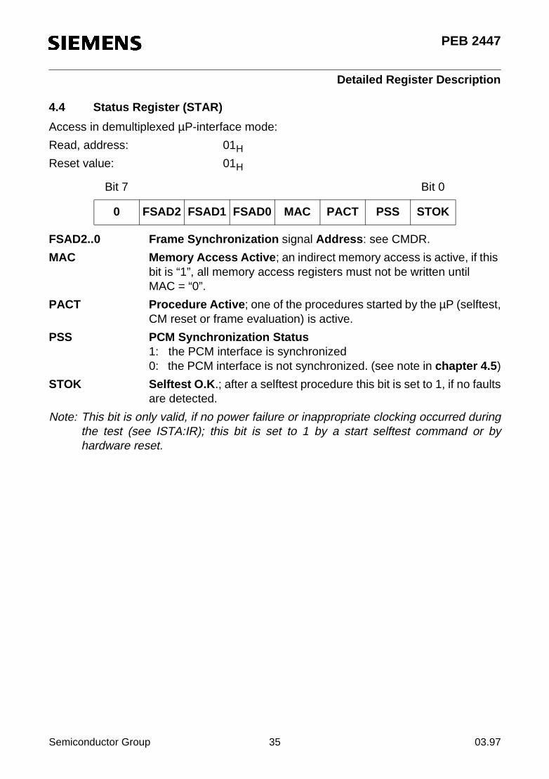
4.4 Status Register (STAR)
Access in demultiplexed µP-interface mode:
Read, address: 01H
Reset value: 01H
FSAD2..0 Frame Synchronization signal Address: see CMDR.
MAC Memory Access Active; an indirect memory access is active, if this bit is “1”, all memory access registers must not be written until MAC = “0”.
PACT Procedure Active; one of the procedures started by the µP (selftest,CM reset or frame evaluation) is active.
PSS PCM Synchronization Status1: the PCM interface is synchronized0: the PCM interface is not synchronized. (see note in chapter 4.5)
STOK Selftest O.K.; after a selftest procedure this bit is set to 1, if no faultsare detected.
Note: This bit is only valid, if no power failure or inappropriate clocking occurred duringthe test (see ISTA:IR); this bit is set to 1 by a start selftest command or byhardware reset.
Bit 7 Bit 0
0 FSAD2 FSAD1 FSAD0 MAC PACT PSS STOK
Semiconductor Group 35 03.97

PEB 2447
Detailed Register Description
4.5 Interrupt Status Register (ISTA)
Access in demultiplexed µP-interface mode:
Read, address: 02H
Reset value: 00H
FEC Frame Evaluation Completed; the indirect register FER contains avalid offset and can be read.
PC Procedure Completed; the procedure started from the commandregister (CM reset or MTSXL selftest) is finished.
IR Initialization Request. The connection memory has to be programmed due to a loss of data (IR = 1). The IR bit is set afterpower failure or inappropriate clocking. It can only be retriggered again after a selftest or CM reset procedure.
PFI PCM Framing Interrupt; this bit being logical 1 indicates the loss orgain of synchronization. Synchronization is considered lost by theMTSXL if the SP signal is not repeated within the correct period.Synchronization is considered achieved, if two consecutive SPpulses with the correct period have been received.
Any interrupt will activate the INT line if it is not masked. All interrupt bits and the INT lineare reset when reading ISTA.
Note 1: All interrupts and the INT line are cleared with reset.
Note 2: If the SP signal is repeated within a multiple of frame length(e.g. 2 × or 4 × 125 µs) but at correct phase:– the MTSXL works correctly because the internal counters run autonomously
and are synchronized within correct phase.– the PFI interrupt does not occur because this situation is internally handled as
“loss of synchronization” and this situation does not change.
Note 3: During selftest no PFI interrupt will occur.
Bit 7 Bit 0
0 0 0 0 FEC PC IR PFI
Semiconductor Group 36 03.97
PEB 2447
Detailed Register Description
4.6 Mask Register (MASK)
Access in demultiplexed µP-interface mode:
Write, address: 02H
Reset value: 0FH
A logical 1 disables the corresponding interrupt as described in ISTA from activating theINT pin. A masked interrupt (bit set to “1”) is stored internally and indicated, when readingISTA. It is also reset in this case.
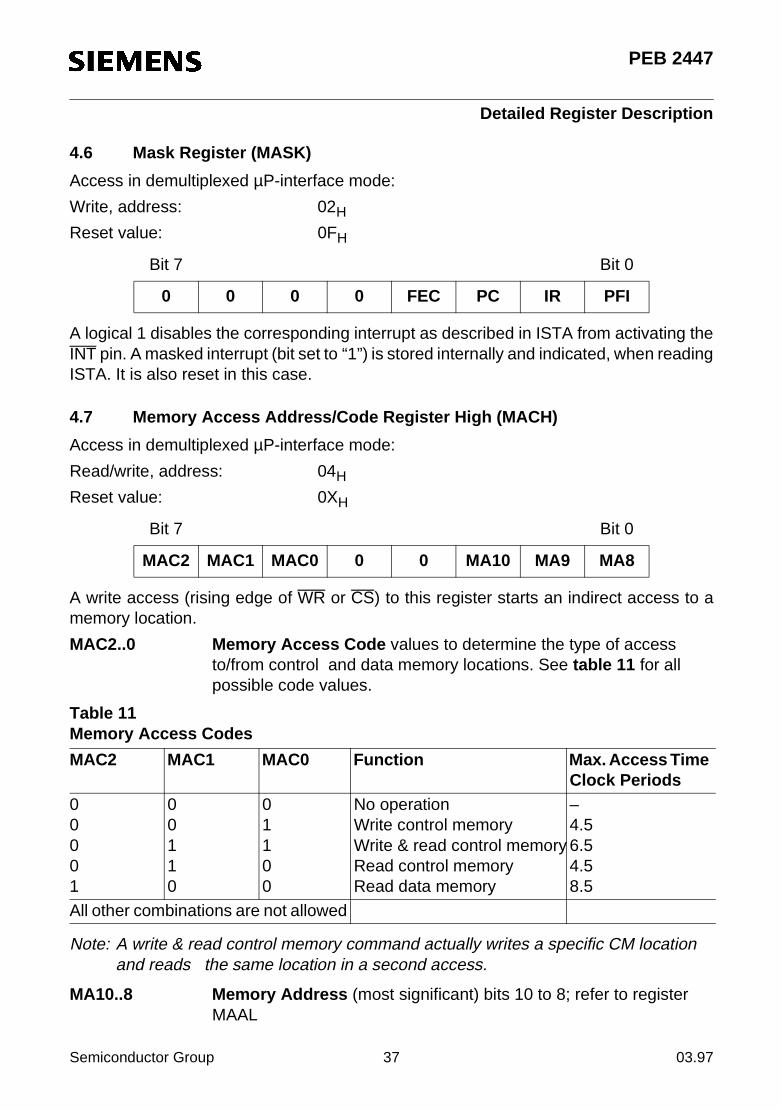
4.7 Memory Access Address/Code Register High (MACH)
Access in demultiplexed µP-interface mode:
Read/write, address: 04H
Reset value: 0XH
A write access (rising edge of WR or CS) to this register starts an indirect access to amemory location.
MAC2..0 Memory Access Code values to determine the type of accessto/from control and data memory locations. See table 11 for allpossible code values.
Note: A write & read control memory command actually writes a specific CM locationand reads the same location in a second access.
MA10..8 Memory Address (most significant) bits 10 to 8; refer to registerMAAL
Bit 7 Bit 0
0 0 0 0 FEC PC IR PFI
Bit 7 Bit 0
MAC2 MAC1 MAC0 0 0 MA10 MA9 MA8
Table 11Memory Access Codes
MAC2 MAC1 MAC0 Function Max. Access Time Clock Periods
00001
00110
01100
No operationWrite control memoryWrite & read control memoryRead control memoryRead data memory
–4.56.54.58.5
All other combinations are not allowed
Semiconductor Group 37 03.97

PEB 2447
Detailed Register Description
4.8 Memory Access Address Register Low (MAAL)
Access in a demultiplexed µP-interface mode:
Read/write, address: 03H
Reset value: XXH
MA7..0 Memory Address bits 7 to 0; the complete memory address is theconcatenation of MA10..0.
If the value MA(10:0) is used as a control memory address, each address correspondsto a single output time slot (see table 12):
Note: Port(m) means, that this port drives the inverted data values of port (m-8). For theoperation “Read Data Memory” MA10..0 are used as data memory addresses withthe same mapping to the input time slots as listed in the above table.
Bit 7 Bit 0
MA7 MA6 MA5 MA4 MA3 MA2 MA1 MA0
Table 12Output Time Slot MappingMode Valid for
Output (Ports)
0 MA10 MA9 MA8 MA7 MA6 MA5 MA4 MA3 MA2 MA1 MA0 OUT (31:0) = Port (31:0)Time Slot Number Port Number
1 MA10 MA9 MA8 MA7 MA6 MA5 MA4 MA3 MA2 MA1 MA0 OUT (7:0) = Port (7:0) OUT (23:16) = Port (15:8)
Time Slot Number6..1 PN3 TS0 PN2..0
3 MA10 MA9 MA8 MA7 MA6 MA5 MA4 MA3 MA2 MA1 MA0 OUT (7:0) = Port (7:0) = Port (15:8)OUT (23:16) = Port (15:8) = Port (31:24)
Time Slot Number6..1 PN3 TS0 PN2..0
Semiconductor Group 38 03.97
PEB 2447
Detailed Register Description
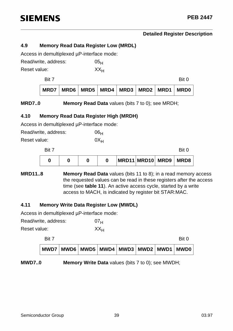
4.9 Memory Read Data Register Low (MRDL)
Access in demultiplexed µP-interface mode:
Read/write, address: 05H
Reset value: XXH
MRD7..0 Memory Read Data values (bits 7 to 0); see MRDH;
4.10 Memory Read Data Register High (MRDH)
Access in demultiplexed µP-interface mode:
Read/write, address: 06H
Reset value: 0XH
MRD11..8 Memory Read Data values (bits 11 to 8); in a read memory accessthe requested values can be read in these registers after the accesstime (see table 11). An active access cycle, started by a writeaccess to MACH, is indicated by register bit STAR:MAC.
4.11 Memory Write Data Register Low (MWDL)
Access in demultiplexed µP-interface mode:
Read/write, address: 07H
Reset value: XXH
MWD7..0 Memory Write Data values (bits 7 to 0); see MWDH;
Bit 7 Bit 0
MRD7 MRD6 MRD5 MRD4 MRD3 MRD2 MRD1 MRD0
Bit 7 Bit 0
0 0 0 0 MRD11 MRD10 MRD9 MRD8
Bit 7 Bit 0
MWD7 MWD6 MWD5 MWD4 MWD3 MWD2 MWD1 MWD0
Semiconductor Group 39 03.97

PEB 2447
Detailed Register Description
4.12 Memory Write Data Register High (MWDH)
Access in demultiplexed µP-interface mode:
Read/write, address: 08H
Reset value: XXH
MWD11..8 Memory Write Data values (bits 11 to 8); in a write memory accessthe values to transfer are written to these registers. Both registersmust not be written during an active access. An active access cycle,started by a write access to MACH, is indicated by register bitSTAR:MAC.
If the values MWD10..0 / MRD10..0 are used as control memory entries, each possiblevalue corresponds to a single input time slot. MWD11 / MRD11 defines, whether theinput time slot is switched actively to the PCM output or is switched to high impedance.
TSC Tristate Control Value0: active1: high impedance; TSC controls whether the output time slot (corresponding to theaddress of the control memory location) will drive the PCM values orwill be tristate.
Bit 7 Bit 0
0 0 0 0 MWD11 MWD10 MWD9 MWD8
Table 13Input Time Slot Mapping / Programming of Output Tristate Control
Mode MRD11..0 / MWD11..0 Valid for Inputs/(Ports)
0 D11 D10 D9 D8 D7 D6 D5 D4 D3 D2 D1 D0 IN (31:0) = Port (31:0)TSC Time Slot Number Port Number
1, 3 D11 D10 D9 D8 D7 D6 D5 D4 D3 D2 D1 D0 IN (23:16) = Port (15:8) IN (7:0) = Port (7:0)
TSC Time Slot Number 6..1 PN3 TS0 PN2..0
Semiconductor Group 40 03.97
PEB 2447
Detailed Register Description
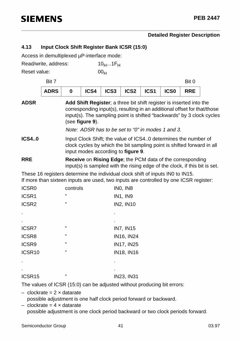
4.13 Input Clock Shift Register Bank ICSR (15:0)
Access in demultiplexed µP-interface mode:
Read/write, address: 10H...1FH
Reset value: 00H
ADSR Add Shift Register; a three bit shift register is inserted into thecorresponding input(s), resulting in an additional offset for that/those input(s). The sampling point is shifted “backwards” by 3 clock cycles(see figure 9).
Note: ADSR has to be set to “0” in modes 1 and 3.
ICS4..0 Input Clock Shift; the value of ICS4..0 determines the number ofclock cycles by which the bit sampling point is shifted forward in allinput modes according to figure 9.
RRE Receive on Rising Edge; the PCM data of the correspondinginput(s) is sampled with the rising edge of the clock, if this bit is set.
These 16 registers determine the individual clock shift of inputs IN0 to IN15.If more than sixteen inputs are used, two inputs are controlled by one ICSR register:
ICSR0 controls IN0, IN8
ICSR1 ” IN1, IN9
ICSR2 ” IN2, IN10
. .
. .
ICSR7 ” IN7, IN15
ICSR8 ” IN16, IN24
ICSR9 ” IN17, IN25
ICSR10 ” IN18, IN16
. .
. .
ICSR15 ” IN23, IN31
The values of ICSR (15:0) can be adjusted without producing bit errors:
– clockrate = 2 × dataratepossible adjustment is one half clock period forward or backward.
– clockrate = 4 × dataratepossible adjustment is one clock period backward or two clock periods forward.
Bit 7 Bit 0
ADRS 0 ICS4 ICS3 ICS2 ICS1 ICS0 RRE
Semiconductor Group 41 03.97
PEB 2447
Detailed Register Description
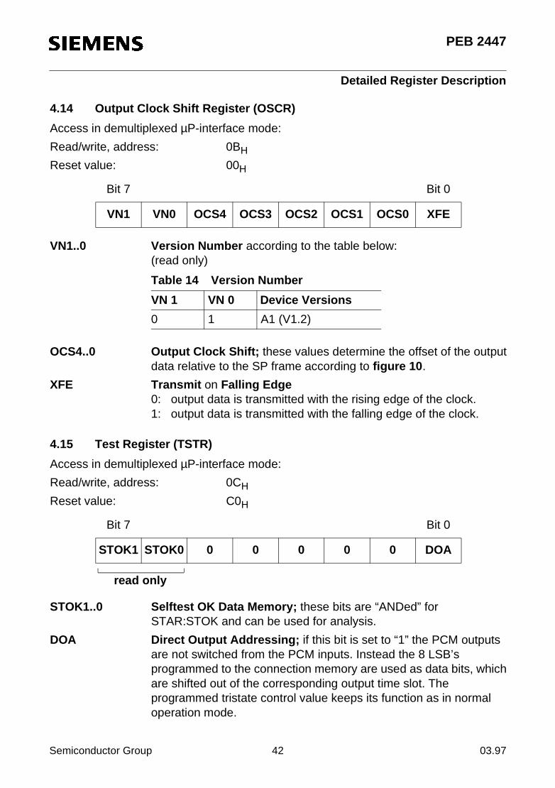
4.14 Output Clock Shift Register (OSCR)
Access in demultiplexed µP-interface mode:
Read/write, address: 0BH
Reset value: 00H
VN1..0 Version Number according to the table below:(read only)
OCS4..0 Output Clock Shift; these values determine the offset of the outputdata relative to the SP frame according to figure 10.
XFE Transmit on Falling Edge0: output data is transmitted with the rising edge of the clock.1: output data is transmitted with the falling edge of the clock.
4.15 Test Register (TSTR)
Access in demultiplexed µP-interface mode:
Read/write, address: 0CH
Reset value: C0H
STOK1..0 Selftest OK Data Memory; these bits are “ANDed” forSTAR:STOK and can be used for analysis.
DOA Direct Output Addressing; if this bit is set to “1” the PCM outputs are not switched from the PCM inputs. Instead the 8 LSB’sprogrammed to the connection memory are used as data bits, whichare shifted out of the corresponding output time slot. Theprogrammed tristate control value keeps its function as in normaloperation mode.
Bit 7 Bit 0
VN1 VN0 OCS4 OCS3 OCS2 OCS1 OCS0 XFE
Table 14 Version Number
VN 1 VN 0 Device Versions
0 1 A1 (V1.2)
Bit 7 Bit 0
STOK1 STOK0 0 0 0 0 0 DOA
read only
Semiconductor Group 42 03.97

PEB 2447
Detailed Register Description
4.16 Frame Evaluation Register Low (FERL)
Access in a demultiplexed µP-interface mode:
Read, address: 0EH
Reset value: XXH
FEV7..0 Frame Evaluation Values (bits 7 to 0); refer to FERH;
4.17 Frame Evaluation Register High (FERH)
Access in demultiplexed µP-interface mode:
Read, address: 0FH
Reset value: XXH
FEV11..0 Frame Evaluation Values; after a frame evaluation procedure (interrupt ISTA:FEC) these two registers contain the offset betweenthe SP frame and an evaluated FS0 ... FS5 frame. The evaluation isperformed at the second following rising edge of FS after thecommand CMDR:SFE = 1 was programmed.
Note: The device must be synchronized to SP (STAR: PSS = 1) inorder to generate a correct result in FERL / FERH.
Note: Time constant “X” is specified to 0 ns < X < 13 ns (see figure 8)
Bit 7 Bit 0
FEV7 FEV6 FEV5 FEV4 FEV3 FEV2 FEV1 FEV0
Bit 7 Bit 0
0 0 0 0 FEV11 FEV10 FEV9 FEV8
Table 15Frame Evaluation Register
CLK / 1.024 MHz Offset Value = FEV11..1 FEV0 FS Rising Edge between
16 Number of clock periods +1
Number of clock periods +1
0
1
Clock rising edge-X ns and clock falling edge-X ns
Clock falling edge-X nsand clock rising edge-X ns
Semiconductor Group 43 03.97
PEB 2447
Electrical Characteristics
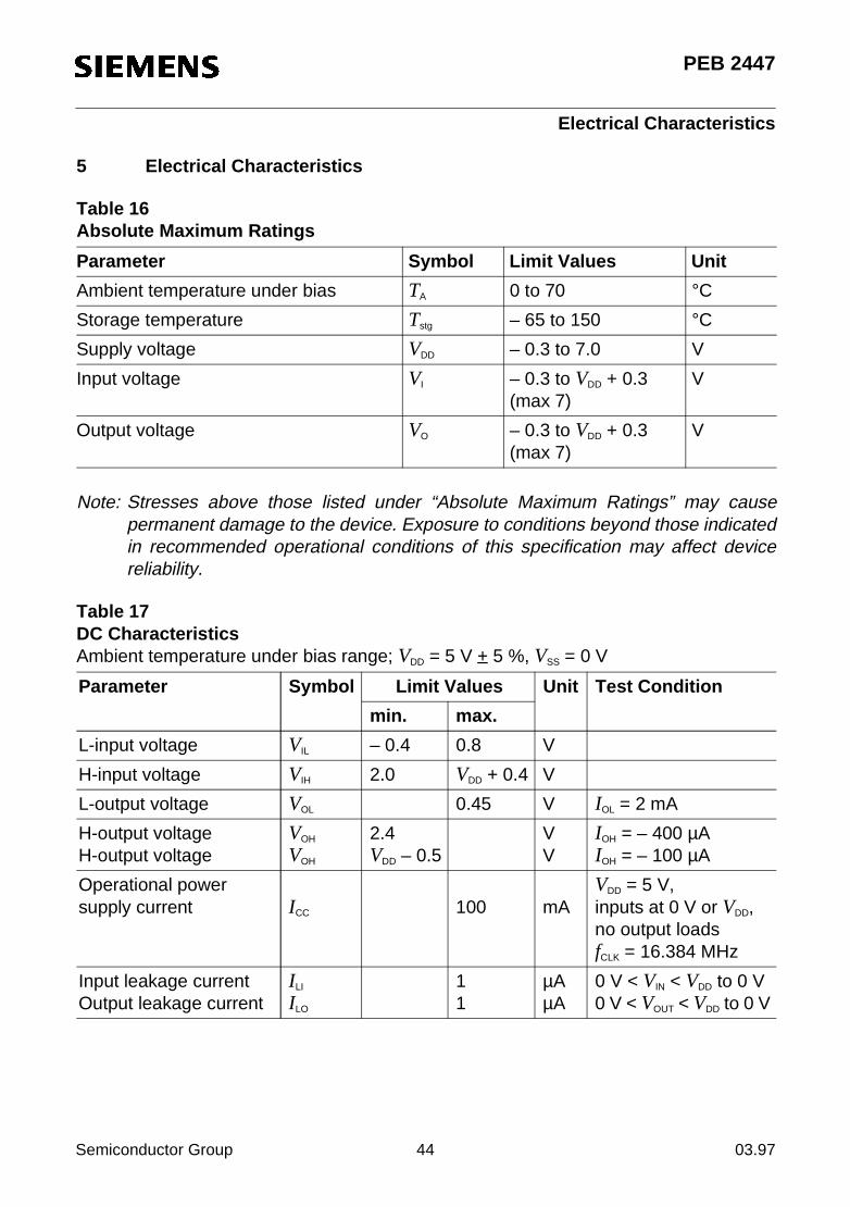
5 Electrical Characteristics
Note: Stresses above those listed under “Absolute Maximum Ratings” may causepermanent damage to the device. Exposure to conditions beyond those indicatedin recommended operational conditions of this specification may affect devicereliability.
Table 16Absolute Maximum Ratings
Parameter Symbol Limit Values Unit
Ambient temperature under bias TA 0 to 70 °C
Storage temperature Tstg – 65 to 150 °C
Supply voltage VDD – 0.3 to 7.0 V
Input voltage VI – 0.3 to VDD + 0.3 (max 7)
V
Output voltage VO – 0.3 to VDD + 0.3 (max 7)
V
Table 17DC CharacteristicsAmbient temperature under bias range; VDD = 5 V + 5 %, VSS = 0 V
Parameter Symbol Limit Values Unit Test Condition
min. max.
L-input voltage VIL – 0.4 0.8 V
H-input voltage VIH 2.0 VDD + 0.4 V
L-output voltage VOL 0.45 V IOL = 2 mA
H-output voltageH-output voltage
VOH
VOH
2.4VDD – 0.5
VV
IOH = – 400 µAIOH = – 100 µA
Operational power supply current ICC 100 mA
VDD = 5 V,inputs at 0 V or VDD, no output loadsfCLK = 16.384 MHz
Input leakage currentOutput leakage current
ILI
ILO
11
µAµA
0 V < VIN < VDD to 0 V0 V < VOUT < VDD to 0 V
Semiconductor Group 44 03.97

PEB 2447
Electrical Characteristics
AC CharacteristicsAmbient temperature under bias range, VDD = 5 V + 5 %.
Inputs are driven at 2.4 V for a logical 1 and at 0.4 V for a logical 0. Timing measurementsare made at 2.0 V for a logical 1 and at 0.8 V for a logical 0. The AC testing input/outputwaveforms are shown below. Timing values are guaranteed for capacitive loading ofCL = 60 pF on all outputs except pins D(7:0), which are specified for CL = 100 pF.
Figure 14I/O Waveform for AC Tests
Table 18CapacitancesTA = 25 °C, VDD = 5 V + 5 %, VSS = 0 V
Parameter Symbol Limit Values Unit
min. max.
Input capacitance CIN 5 pF
Output capacitance COUT 10 pF
I/O capacitance CIO 15 pF
Semiconductor Group 45 03.97
PEB 2447
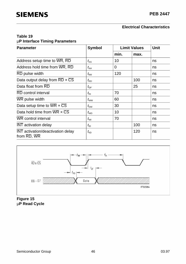
Electrical Characteristics
Figure 15µP Read Cycle
Table 19µP Interface Timing Parameters
Parameter Symbol Limit Values Unit
min. max.
Address setup time to WR, RD tAS 10 ns
Address hold time from WR, RD tAH 0 ns
RD pulse width tRR 120 ns
Data output delay from RD × CS tRD 100 ns
Data float from RD tDF 25 ns
RD control interval tRI 70 ns
WR pulse width tWW 60 ns
Data setup time to WR × CS tDW 30 ns
Data hold time from WR × CS tWD 10 ns
WR control interval tWI 70 ns
INT activation delay tID 100 ns
INT activation/deactivation delay from RD, WR
tIID 120 ns
Semiconductor Group 46 03.97

PEB 2447
Electrical Characteristics
Figure 16µP Write Cycle
Figure 17Demultiplexed Address Timing
Figure 18Interrupt Timing
Semiconductor Group 47 03.97

PEB 2447
Electrical Characteristics
Table 20 PCM Interface Characteristics
Parameter Symbol Limit Values Unit Condition
min. max.
Clock periodClock period lowClock period high
tCP
tCPL
tCPH
602727
nsnsns
Frame setup timeFrame hold time
tFS
tFH
720
nsns
Serial data input setup timeSerial data input hold time
tS
tH
920
nsns
PCM serial data output delay time tD 50 ns
Semiconductor Group 48 03.97

PEB 2447
Electrical Characteristics
Figure 19AC Characteristics at the PCM Interface
Semiconductor Group 49 03.97

PEB 2447
Electrical Characteristics
Figure 20AC Characteristics at Boundary Scan Interface
Table 21Boundary Scan Timing
Parameter Symbol Limit Values Unit Condition
min. max.
Test clock period tTCP 160 ns
Test clock period low tTCPL 80 ns
Test clock period high tTCPH 80 ns
TMS setup time to TCK tMSS 30 ns
TMS hold time from TCK tMSH 30 ns
TDI setup time to TCK tDIS 30 ns
TDI hold time from TCK tDIH 30 ns
TDO delay from TCK tDOD 60 ns
Semiconductor Group 50 03.97
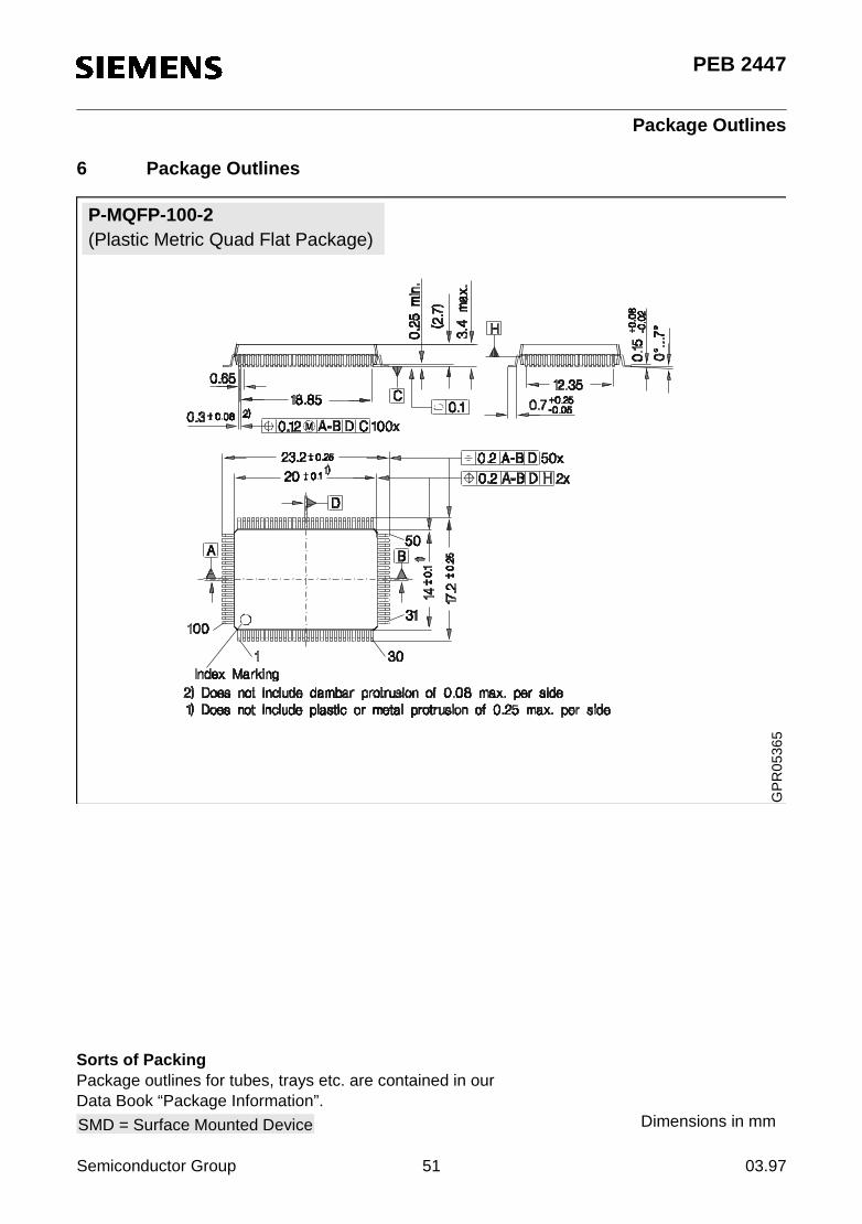
PEB 2447
Package Outlines
6 Package Outlines
P-MQFP-100-2(Plastic Metric Quad Flat Package)
GP
R05
365
Sorts of PackingPackage outlines for tubes, trays etc. are contained in our Data Book “Package Information”.
Dimensions in mmSMD = Surface Mounted Device
Semiconductor Group 51 03.97


![Evaluation board based on the STHV64SW high voltage switch ... › a6ed › A700000006582547.pdf · L2 2 OUT5 L4 IN3 K2 OUT15 OUT12 L6 3 11 IN[0..15] 19 IN1 30 OUT7 27 13 ClassName:](https://static.documents.pub/doc/80x56/5f10d3977e708231d44b010b/evaluation-board-based-on-the-sthv64sw-high-voltage-switch-a-a6ed-a-a700000006582547pdf.jpg)


