34
IEEE 1149.1/JTAG TDRs which cross power domains require control cells and muxes CJ Clark, Intellitech Corp. 10/14/2011 1 For IEEE 1149.1/JTAG WG Review
| Date post: | 03-Sep-2018 |
| Category: |
Documents |
| Upload: | dinhnguyet |
| View: | 243 times |
| Download: | 0 times |

IEEE 1149.1/JTAG TDRs which cross power domains require control cells and muxes
CJ Clark, Intellitech Corp.
10/14/2011 1
For IEEE 1149.1/JTAG WG Review

10/14/2011 2
Muxes in 1149.1 are not new. IR and TDRs have been muxed within the IC since the standard originated Linking devices link via muxes

IDCODE
32
6
IDCODE
32
6
IDCODE
32
6
IRScan = 18
DRScan = 96
IDCODE
32
6
bypass
1
6
IDCODE
32
6
IRScan = 18
DRScan = 65
Recall that Board level scan-chains – loading bypass as an IR scan changes length by 31 bits for the subsequent DR scans - tracking lengths of chains and muxing of TDRs has been with us for some time
10/14/2011 3

IDCODE
32
6
IDCODE
32
6
IDCODE
32
6
IRScan = 12
DRScan = 32 + 8 = 40
Scan ‘linking’ devices have been known since 1990 - most tools know how to support these - 4 to 16 paths or ‘rings’ in the chain or in idle/TLR
LINK
6
8 SELDR
TDI TDO
1 Many Details omitted
10/14/2011 4
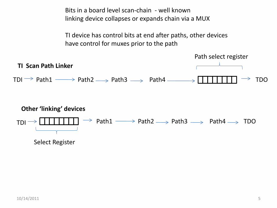
Path select register
Bits in a board level scan-chain - well known linking device collapses or expands chain via a MUX TI device has control bits at end after paths, other devices have control for muxes prior to the path
Path1 Path2 Path3 Path4 TDI TDO
TI Scan Path Linker
Select Register
Path1 Path2 Path3 Path4 TDI TDO
Other ‘linking’ devices
10/14/2011 5

10/14/2011 6
Why can't the Boundary Register be in the same power domain as the TAP?

10/14/2011 7
Power1 Power2
Power3
Power4
Power5 Power6
Power7
Power8
Without segmentation, If one part of boundary register crosses an area where there is no power (due to defect, dc/dc off, etc) then the whole boundary register is un-scannable. This design is compliant as far as I know, but a single power defect corrupts the entire boundary register contents.
The IC power today is segmented (cores and I/O)
DC/DC
DC/DC
Fault

10/14/2011 8
Power1 Power2
Power3
Power4
Power5 Power6
Power7
Power8
Is there any part of this design which is non-compliant? - I don’t think so, but a single fault from power or external power is 'off' will prevent scanning the b-s register.
DC/DC
DC/DC
Fault

10/14/2011 9
The standard mandates and recommends b-s cells with a view that I/O IP must be delivered separately from the cells - this limits the choices the industry has and the ease of design
IO Vref
Sig+
Sig-
I/O power domain Boundary scan chain power domain
enable
sig cell
power isolation cells/level shift

10/14/2011 10
challenges exist for having observe cells on a leg and keep it in the 'TAP' or 'boundary scan' power domain (distance, isolation, leakage etc)
IO Vref
Sig+
Sig-
I/O power domain
Boundary scan chain power domain
enable
sig cell
power isolation cells/level shift
T-switch Extest

10/14/2011 11
Now add INIT_DATA input to the SERDES, for voltage, protocol, pre-emphasis, etc. How many power isolation cells and level shifter are needed by the designer?
I/O power domain
Boundary scan chain power domain
power isolation cells/level shift
IO Vref Sig+
Sig-
enable
sig cell
T-switch Extest
INIT_DATA Cells
Explosion in count of level shifters and power isolation cells as so many signals have to cross to the 'TAP' power domain

10/14/2011 12
What about IP that has integrated b-s cells? - require b-s cells on the n-bit parallel interface? - 40 b-s cells?
IO Vref
Sig+
Sig-
I/O power domain Boundary scan chain power domain
40 bit PISO
integrated B-s cell in IP How to use and keep powered?
How to use the 40bit PISO interface?

10/14/2011 13
By allowing boundary and INIT_DATA in the IO power domain, the job is easier - Fewer Level shifters/isolation cells
I/O power domain TAP domain
Only one set of Clause 9 1149.1 signals for many I/O need to traverse the domain. TCK capture_<tdr> update_<tdr> shift_<tdr> reset_<tdr> SI/SO for INIT_DATA and boundary (or gated clock equivalent) + Mode/chmode
Many I/O to few power domain crossings is easier, routing easier area easier

10/14/2011 14
Power1 Power2
Power3
Power4
Power5 Power6
Power7
Power8
OK, the boundary register is shown around the edge, which is not typical of today's IC. (bear with me)
Segmentation offers several advantages. - easier for IC designer to manage I/O in multiple power domains (Our standard has to be practical for today's designs)
DC/DC
DC/DC
Test engineer can isolate the fault to a segment/area

10/14/2011 15
Segmentation offers new segmented EXTEST capabilities - the ad-hoc use has been discussed in papers - vendors don’t need support it if you don’t see the benefit
Power1 Power2
Power5 Power6
Power7
Power8
DC/DC
DC/DC
IC segments in mission mode
Two IC segments in test mode

10/14/2011 16
But, the full boundary scan register has served us well for 20+ years - yes it has. Now we have to be realistic about the problems associated with the b-s register (or init_data) in a single power domain We're going to far, I don’t want to modify my software - Our standard isn't useful if the $300Billion IC industry doesn’t follow it or has non-compliant ICs. It would be disproportionate in terms of cost for semiconductor vendors to spend more money (design time and area) on EACH IC design to overcome the power domain problem because a small segment of tool vendors with more representation on the WG don’t want to support parsing two special bits of each b-s segment. Both values must be a '1' to keep the mux 'ON' and the power 'on'. Simply scan those values in all the time as if they were internal cells in a BOUNDARY_REGISTER description.

10/14/2011 17
What do we need to add to TDRs to support the TDR crossing a power domain?

10/14/2011 18
Two TDR cells needed prior to crossing the power domain - cells are defined by REGISTER_FIELDS in BSDL
A 'power' cell as shown in figure 9-6 of draft. The Power state (on/off) is captured at PI of the cell and the power state is turned on/off at PO. (Power observation is through level shifter)
Capture_<TDR>
SHIFT_<TDR>
SO
0
1
0
1
Update_<TDR>
TCK
RESET_<TDR>
0
1
PO
Q
QSET
CLR
DQ
QSET
CLR
D
To next bit
From Last Bit
A control cell is a selfmon type cell, the output of the cell is captured (PI to PO in figure 9-6 of draft.) The control cell (cmux) controls the mux to insert or remove a segment.
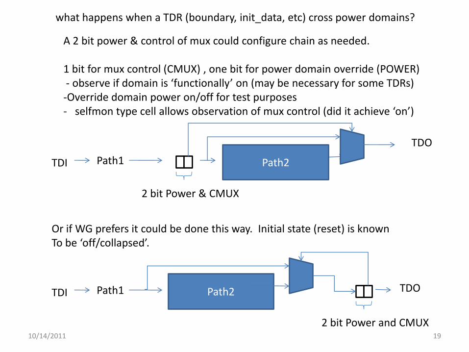
what happens when a TDR (boundary, init_data, etc) cross power domains?
2 bit Power & CMUX
Path1 Path2 TDI
TDO
Path2
2 bit Power and CMUX
Path1 Path2 TDI TDO Path2
Or if WG prefers it could be done this way. Initial state (reset) is known To be ‘off/collapsed’.
A 2 bit power & control of mux could configure chain as needed. 1 bit for mux control (CMUX) , one bit for power domain override (POWER) - observe if domain is ‘functionally’ on (may be necessary for some TDRs) -Override domain power on/off for test purposes - selfmon type cell allows observation of mux control (did it achieve ‘on’)
10/14/2011 19

TDR segments within an IC
TDO
Power_mux
TDR Power Domain
Path2
Path1 TDI
Mux Control
Power_sense
Rules: Mux and cells are always outside of Power Domain Power mux cells control mux on ‘other side’ of domain prior to next Power Mux or TDO (No power_mux around another power mux) 2 bits, one cell controls mux and other is optional to override system which may have power domain off.
0 1
Capupd cell
A capupd cell is one of the cells we have not allowed yet as a pre-defined Cell like NOPI or NOPO. CAPUPD captures from the update register. The mux Control is a critical signal that needs testability . One could argue that Power_sense Could be used instead of UPD as the capture value. One could also argue that The cells after the Path2 must be used for obtaining value from CAPUPD on mux control
10/14/2011 20

TDR segments within an IC
TDO
Power_mux
TDR Power Domain
Path2
Path1 TDI
Mux Control
Power_sense
0 1
Capupd cell
10/14/2011 21
But it's too simple, it's not showing the power controller, Isolation cells (ISO), Level Shifters (LS), and Retention Registers (RR). That's right. 1149.1 would be mute on forcing the designer to design it a certain way. The only thing we are defining is that there is a power observe, a power override and a separate self-monitoring cell which controls the mux. The definition of the control cell for the mux is that it powers up in the 'off' state, the mux with the short path on.

BOUNDARY REGISTER TDR segments within an IC - mode is gated with CMUX output
TDO
Power Cell
TDR Power Domain
Path2
Path1 TDI
MUX
Power_sense (capture via Power cell)
0 1
CMUX cell (selfmon)
10/14/2011 22
mode (EXTEST =1)
to b-s cells

10/14/2011 23
How can we describe this?

attribute REGISTER_ASSEMBLY of chip_2011 : entity is "INIT_DATA ( "& -- TDI "(USING SerdesO),( i1 IS init_data DEFAULT.ALLBITS (CHPMFG(Test)) ), "& "(USING SerdesO),( i2 IS init_data DEFAULT.ALLBITS (CHPMFG(Test)) ), "& "(USING SerdesH),( i3 IS init_data DEFAULT.ALLBITS (CHPMFG(Test)) ), "& "(USING SerdesO),( i4 IS init_data DEFAULT.BSTERM (BSTERM(CPflt)) DEFAULT.BSCM (BSCM(DC_CPL)) DEFAULT.BSSWING (BSSWING(1115mV)) ) "& -- TDO ")"; REGISTER_ASSEMBLY with i1, i2, i3 and i4 provide 4 x 6 bits or 24 bits of scan data. (John Siebold example, recall SERDESH and SERDESO have a 6 bit tdr segment).
REGISTER_ASSEMBLY has been proposed and accepted - Scan chain length deferred and calculated from R_A
10/14/2011 24

attribute REGISTER_ASSEMBLY of chip_2011 : entity is "INIT_DATA ( "& -- TDI "(USING SerdesO),( i1 IS init_data DEFAULT.ALLBITS (CHPMFG(Test)) ), "& "(USING SerdesO),( i2 IS init_data DEFAULT.ALLBITS (CHPMFG(Test)) ), "& -- i3 is missing or commented out "(USING SerdesO),( i4 IS init_data DEFAULT.BSTERM (BSTERM(CPflt)) DEFAULT.BSCM (BSCM(DC_CPL)) DEFAULT.BSSWING (BSSWING(1115mV)) ) "& -- TDO ")"; A tool which knows how to read REGISTER_ASSEMBLY and found only i1, i2 and i4 would calculate that there are 3 x 6 bits or 18 bits of scan data. (John Siebold example, recall SERDESH and SERDESO have a 6 bit tdr segment). A tool could programmatically allow one to add to R_A or subtract from it.
Recall that without i3 in the description the same process Takes place of reading the instances and totaling up the Lengths.
10/14/2011 25

It’s possible for 1149.1-2012 package file to specify the POWER, CMUX and
MUX. One bit senses power domain and enables control, the other bit
controls the mux.
attribute REGISTER_MNEMONICS of std_1149_1_2012 : package is
“MUX (On (1) < chain segment is included >, " &
" Off (0) < chain segment not included >), " &
“POWER (On (1) < Domain is functionally on> ), " &
“ Off (0) < Domain is functionally off>), “ &
“CONTROL (Override (1) < Test controls domain power to ON > ), " &
“ Normal (0) < Power domain in normal mode> )“;
attribute REGISTER_FIELDS of std_1149_1_2012 : package is
“POWER[1] ( "&
"(DOMAIN [1] IS (0 ) DEFAULT(CONTROL(Normal)) “ &
“ RESETVAL(Control(Normal)), "&
“ CAPTURES(POWER(-)) ) "&
")," &
“CONTROL[1] ( "&
"(CMUX [1] IS (0 ) DEFAULT(MUX(Off) ), "&
“ RESETVAL(MUX(Off) ),”&
“ SELFMON ) ”&
")," &
“MUX[0] ( "&
"(MUX [0] IS (0 ) ) "&
" )";
10/14/2011 26
at POR/RESET domain is in 'normal' mode
at POR/RESET mux control is in 'off' mode - segment not included

• Note that one cell, the domain cell is responsible for sensing and overriding power
independent of mux cell. - if power does not come on due to 1) fault 2) board constraint SAMPLE based scan-chain test done first. (some faults not seen until
board ICs are in EXTEST though) Test software can fail immediately at this point. Test engineer would
not expand and turn on domain. - diagnostic software could run smaller interconnect test with smaller number of domains 'on'.
10/14/2011 27

attribute REGISTER_ASSEMBLY of chip_2011 : entity is "INIT_DATA ( "& -- TDI "(USING SerdesO),( i1 IS init_data DEFAULT.ALLBITS (CHPMFG(Test)) ), "& "(USING SerdesO),( i2 IS init_data DEFAULT.ALLBITS (CHPMFG(Test)) ), "& "(USING STD_1149_1_2012), “& “( P1 IS POWER CHRESET ), "& “( c1 IS CONTROL CHRESET ), "& "(USING SerdesH),( i3 IS init_data DEFAULT.ALLBITS (CHPMFG(Test)) ), "& "(USING SerdesO),( i4 IS init_data DEFAULT.BSTERM (BSTERM(CPflt)) DEFAULT.BSCM (BSCM(DC_CPL)) DEFAULT.BSSWING (BSSWING(1115mV)) ) "& -- TDO “( mux1 IS MUX ), "& ")";
Use of POWER & MUX in R_A
Consider if SERDESH is in a separate POWER Domain
10/14/2011 28
this portion is on/off depending on domain and mux register_fields of the Powermux (see package file descriptions on prior page

1) For power segments which can be observed or control/observed, at least one POWER TDR bit and Control (CMUX) cell is required per segment. 2) The segment is defined between the CONTROL and the MUX 3) There must always be a pair of CONTROL and MUX 4) CONTROL (CMUX) cell bits are always reset to the short, collapsed segment 5) MUX is a zero bit field and is used to indicate where the mux in the TDR exists 6) there is no overlap/heirarchy
Basic Rules/Operation
10/14/2011 29

10/14/2011 30
attribute BOUNDARY_REGISTER_SEGMENT of east : entity is -- num cell port function safe [ccell disval rslt] "10 (BC_1, *, controlr, X )," &
"9 (BC_1, D(0), input, X, PULL0)," &
"8 (BC_1, D(1), input, X, PULL0)," &
"7 (BC_1, Q(1), output3, X, 10, 1, PULL0 )," & "6 (BC_1, Q(2), output3, X, 10, 1, PULL0 )," &
"5 (BC_1, Q(3), output3, X, 10, 1, PULL0 )," &
"4 (BC_1, Q(4), output3, X, 10, 1, PULL0 )," &
"3 (BC_1, Q(5), output3, X, 10, 1, PULL0 )," &
"2 (BC_1, Q(6), output3, X, 10, 1, PULL0 )," &
"1 (BC_1, Q(7), output3, X, 10, 1, PULL0 )," &
"0 (BC_1, Q(8), output3, X, 10, 1, PULL0 )";
attribute BOUNDARY_REGISTER_SEGMENT of west : entity is -- num cell port function safe [ccell disval rslt] "10 (BC_1, *, controlr, X )," &
"9 (BC_1, D(2), input, PULL0)," &
"8 (BC_1, D(3), input, PULL0)," &
"7 (BC_1, Q(9), output3, X, 10, 1, PULL0 )," & "6 (BC_1, Q(10), output3, X, 10, 1, PULL0 )," &
"5 (BC_1, Q(11), output3, X, 10, 1, PULL0 )," &
"4 (BC_1, Q(12), output3, X, 10, 1, PULL0 )," &
"3 (BC_1, Q(13), output3, X, 10, 1, PULL0 )," &
"2 (BC_1, Q(14), output3, X, 10, 1, PULL0 )," &
"1 (BC_1, Q(15), output3, X, 10, 1, PULL0 )," &
"0 (BC_1, Q(16), output3, X, 10, 1, PULL0 )";
attribute BOUNDARY_REGISTER_SEGMENT of south : entity is -- num cell port function safe [ccell disval rslt] "10 (BC_1, *, controlr, X )," &
"9 (BC_1, D(4), input, PULL0)," &
"8 (BC_1, D(5), input, PULL0)," &
"7 (BC_1, Q(17), output3, X, 10, 1, PULL0 )," & . "6 (BC_1, Q(18), output3, X, 10, 1, PULL0 )," &
"5 (BC_1, Q(19), output3, X, 10, 1, PULL0 )," &
"4 (BC_1, Q(20), output3, X, 10, 1, PULL0 )," &
"3 (BC_1, Q(21), output3, X, 10, 1, PULL0 )," &
"2 (BC_1, Q(22), output3, X, 10, 1, PULL0 )," &
"1 (BC_1, Q(23), output3, X, 10, 1, PULL0 )," &
"0 (BC_1, Q(24), output3, X, 10, 1, PULL0 )";
attribute BOUNDARY_REGISTER_SEGMENT of north : entity is -- num cell port function safe [ccell disval rslt] "10 (BC_1, *, controlr, X )," &
"9 (BC_1, D(6), input, PULL0)," &
"8 (BC_1, D(7), input, PULL0)," &
"7 (BC_1, Q(25), output3, X, 10, 1, PULL0 )," & "6 (BC_1, Q(26), output3, X, 10, 1, PULL0 )," &
"5 (BC_1, Q(27), output3, X, 10, 1, PULL0 )," &
"4 (BC_1, Q(28), output3, X, 10, 1, PULL0 )," &
"3 (BC_1, Q(29), output3, X, 10, 1, PULL0 )," &
"2 (BC_1, Q(30), output3, X, 10, 1, PULL0 )," &
"1 (BC_1, Q(31), output3, X, 10, 1, PULL0 )," &
"0 (BC_1, Q(32), output3, X, 10, 1, PULL0 )";
TDRs can be built using R_A and R_F, however boundary registers do not follow R_F format. BOUNDARY_REGISTER_SEGMENT enables R_A to be used with the bscan register Here we have 4 B-R segments. Control cells for all I/O have to be within the segment number is local to the segment

10/14/2011 31
attribute REGISTER_ASSEMBLY of chip_2012 : entity is
"BOUNDARY ( "&
-- TDI
"( p1 IS POWER ), ( c1 IS CONTROL ), "&
"( i1 IS east ), "&
"( mux1 IS MUX ), "& -- zero bits
"( p2 IS POWER ), ( c2 IS CONTROL ),"&
"( i2 IS south ), "&
"( mux2 IS MUX ), "& -- zero bits. Note NESTING is not allowed.
"( M1 IS misc ), "& -
"( p3 IS POWER ), ( c3 IS CONTROL ),"&
"( i3 IS west ), "&
"( mux3 IS MUX ), "& -- contributes no bits to the scan chain
"( p4 IS POWER ), ( c4 IS CONTROL ),"&
"( i4 IS north )"&
"( i4 IS MUX ), "& -- no bits in scan chain – just the return path
"( M2 IS misc ), "& -- additional pins/cells in TAP power domain
-- TDO
")";
Power Must be on
Need to support register_assembly already for INIT_DATA and user TDRs - could be handy for BSCAN register - when init_data is present both registers need power mux

10/14/2011 32
I'm worried that the b-s register will become corrupt with these mux control bits - recall the original figure. be more worried of the effects of a single b-s register with segmented power.
Power1 Power2
Power3
Power4
Power5 Power6
Power7
Power8 DC/DC
DC/DC
Fault
recall also that - a '0' shifted into an internal cell position in the boundary register can also corrupt the b-s register contents. " 197 ( BC_1 , *, internal , 1 ) , " & " 198 ( BC_1 , *, internal , 1 ) , " & it's been manageable for 20+ years now to get these bits set right

10/14/2011 33
attribute REGISTER_MNEMONICS of std_1149_1_2012 : package is
“MUX (On (1) < chain segment is included >, " &
" Off (0) < chain segment not included >), " &
“POWER (On (1) < Domain is functionally on> ), " &
“ Off (0) < Domain is functionally off>), “ &
“CONTROL (Override (1) < Test controls domain power to ON > ), " &
“ Normal (0) < Power domain in normal mode> )“;
attribute REGISTER_FIELDS of std_1149_1_2012 : package is
“POWER[1] ( "&
"(DOMAIN [1] IS (0 ) DEFAULT(CONTROL(Normal)) “ &
“ RESETVAL(Control(Normal)), "&
“ CAPTURES(POWER(-)) ) "&
")," &
“CONTROL[1] ( "&
"(CMUX [1] IS (0 ) DEFAULT(MUX(Off) ), "&
“ RESETVAL(MUX(Off) ),”&
“ SELFMON ) ”&
")," &
“MUX[0] ( "&
"(MUX [0] IS (0 ) ) "&
" )";
attribute REGISTER_ASSEMBLY of chip_2012 : entity is
"BOUNDARY ( "&
-- TDI
"( p1 IS POWER ), ( c1 IS CONTROL ), "&
"( i1 IS east ), "&
"( mux1 IS MUX ), "& -- zero bits
"( p2 IS POWER ), ( c2 IS CONTROL ),"&
"( i2 IS south ), "&
"( mux2 IS MUX ), "& -- zero bits. Note NESTING is not allowed.
"( M1 IS misc ), "& -
"( p3 IS POWER ), ( c3 IS CONTROL ),"&
"( i3 IS west ), "&
"( mux3 IS MUX ), "& -- contributes no bits to the scan chain
"( p4 IS POWER ), ( c4 IS CONTROL ),"&
"( i4 IS north )"&
"( i4 IS MUX ), "& -- no bits in scan chain – just the return path
"( M2 IS misc ), "& -- additional pins/cells in TAP power domain
-- TDO
")";
PDL - what a tool should do
# turn on P1 power domain iWrite p1.domain Override iWrite p2.domain OVerride iApply # check it is on iRead p1.domain On iRead p2.domain On iApply -loopuntil pass # turn on mux iWrite p1.cmux On iApply

10/14/2011 34
attribute REGISTER_MNEMONICS of std_1149_1_2012 : package is
“MUX (On (1) < chain segment is included >, " &
" Off (0) < chain segment not included >), " &
“POWER (On (1) < Domain is functionally on> ), " &
“ Off (0) < Domain is functionally off>), “ &
“CONTROL (Override (1) < Test controls domain power to ON > ), " &
“ Normal (0) < Power domain in normal mode> )“;
attribute REGISTER_FIELDS of std_1149_1_2012 : package is
“POWER[1] ( "&
"(DOMAIN [1] IS (0 ) DEFAULT(CONTROL(Normal)) “ &
“ RESETVAL(Control(Normal)), "&
“ CAPTURES(POWER(-)) ) "&
")," &
“CONTROL[1] ( "&
"(CMUX [1] IS (0 ) DEFAULT(MUX(Off) ), "&
“ RESETVAL(MUX(Off) ),”&
“ SELFMON ) ”&
")," &
“MUX[0] ( "&
"(MUX [0] IS (0 ) ) "&
" )";
attribute REGISTER_ASSEMBLY of chip_2012 : entity is
"BOUNDARY ( "&
-- TDI
"( p1 IS POWER ), ( c1 IS CONTROL ), "&
"( i1 IS east ), "&
"( mux1 IS MUX ), "& -- zero bits
"( p2 IS POWER ), ( c2 IS CONTROL ),"&
"( i2 IS south ), "&
"( mux2 IS MUX ), "& -- zero bits. Note NESTING is not allowed.
"( M1 IS misc ), "& -
"( p3 IS POWER ), ( c3 IS CONTROL ),"&
"( i3 IS west ), "&
"( mux3 IS MUX ), "& -- contributes no bits to the scan chain
"( p4 IS POWER ), ( c4 IS CONTROL ),"&
"( i4 IS north )"&
"( i4 IS MUX ), "& -- no bits in scan chain – just the return path
"( M2 IS misc ), "& -- additional pins/cells in TAP power domain
-- TDO
")";
# turn on P1 power domain iWrite p1.domain Override iApply #wait for a bit iRunLoop 1000 # iWrite p1.myspecialcell iApply #wait for a bit iRunLoop 1000 # check it is on iRead p1.domain On iApply # turn on mux iWrite p1.cmux On iApply
Custom sequences would have to be manually described in PDL


