19
IEEE-1394 Data Link Design Review Sherry Womack Erik Pace ECE 4040 Dr. Martin Brooke
| Date post: | 24-Dec-2015 |
| Category: |
Documents |
| Upload: | primrose-greene |
| View: | 225 times |
| Download: | 3 times |

IEEE-1394 Data Link
Design ReviewSherry Womack
Erik Pace
ECE 4040
Dr. Martin Brooke
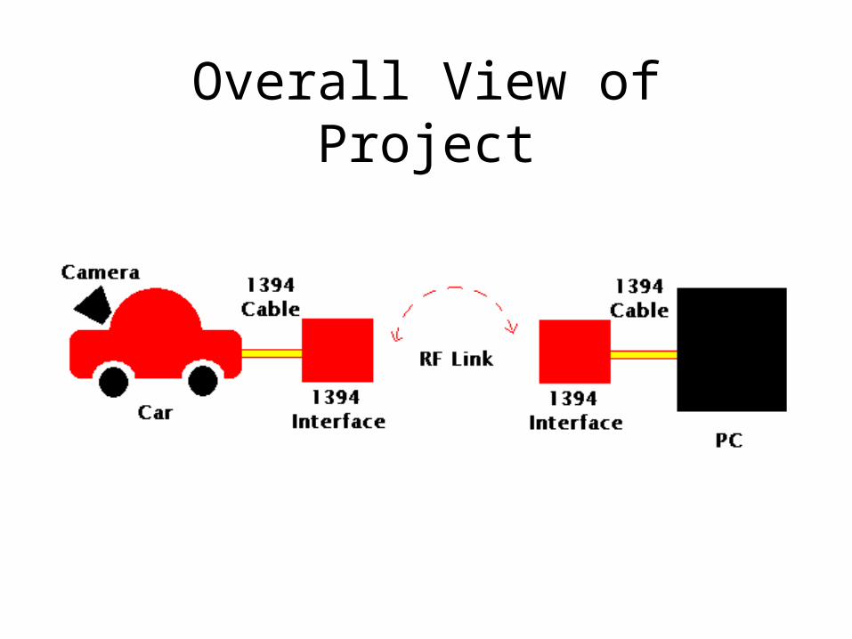
Overall View of Project

Introduction
• What is IEEE-1394?
– FireWire– IEEE 1394-1995 Standard for a High
Performance Serial Bus.– A standard for high-speed data communication
between multimedia products.
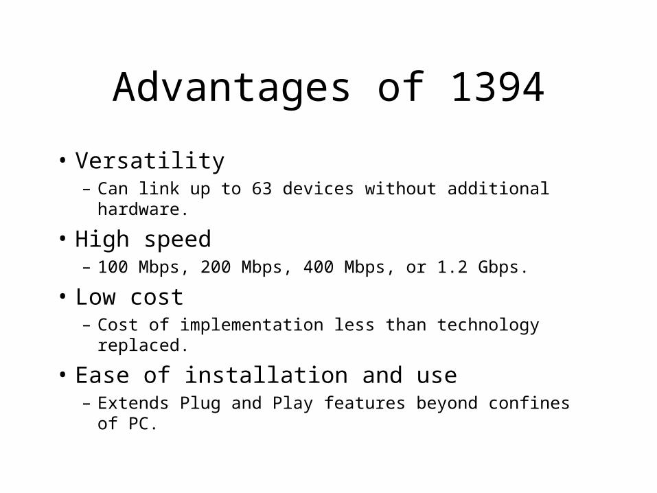
Advantages of 1394
• Versatility– Can link up to 63 devices without additional hardware.
• High speed– 100 Mbps, 200 Mbps, 400 Mbps, or 1.2 Gbps.
• Low cost– Cost of implementation less than technology replaced.
• Ease of installation and use– Extends Plug and Play features beyond confines of PC.
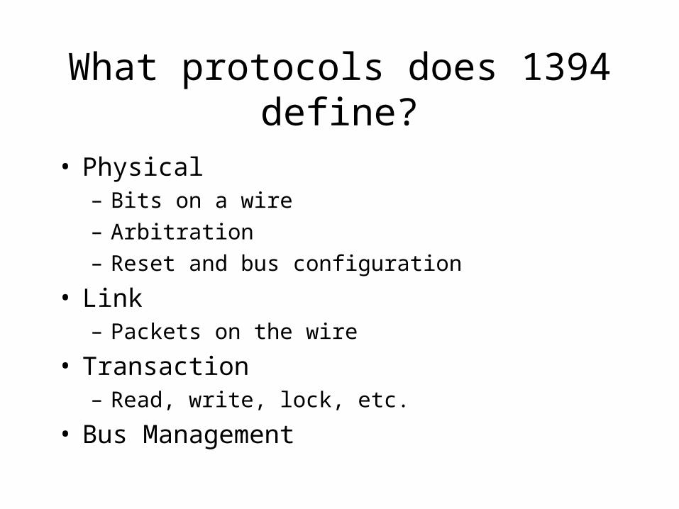
What protocols does 1394 define?
• Physical– Bits on a wire
– Arbitration
– Reset and bus configuration
• Link– Packets on the wire
• Transaction– Read, write, lock, etc.
• Bus Management
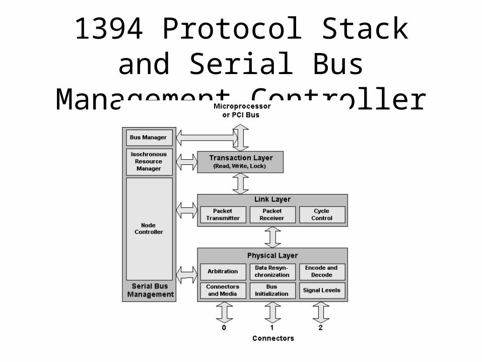
1394 Protocol Stack and Serial Bus Management Controller

Physical Layer Chip
• TSB41LV03A IEEE 1394a Three-Port Cable Transceiver/Arbiter.
• Provides digital and analog transceiver functions needed to implement a 1394 network.
• Includes circuitry to monitor line conditions, for initialization and arbitration, and for packet reception and transmission.
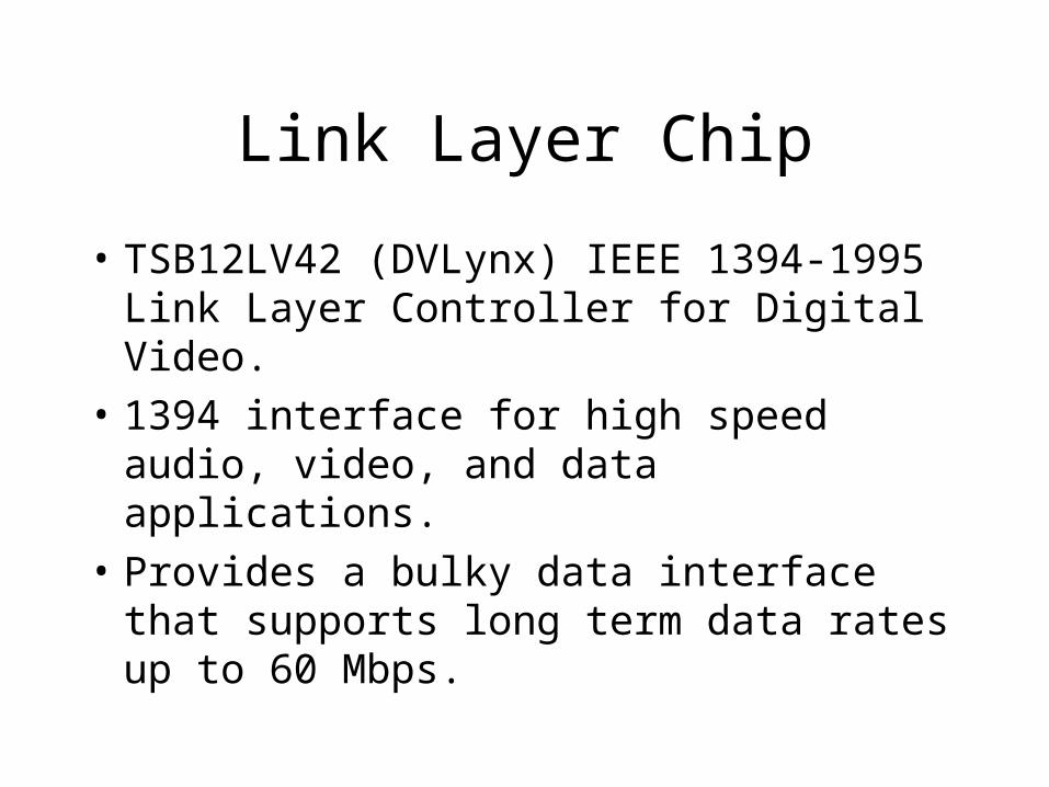
Link Layer Chip
• TSB12LV42 (DVLynx) IEEE 1394-1995 Link Layer Controller for Digital Video.
• 1394 interface for high speed audio, video, and data applications.
• Provides a bulky data interface that supports long term data rates up to 60 Mbps.

Physical and Link Layer Connections

Cable Connections and Power Decoupling Network

Components

Vendors
• DigiKey
• Linear Technology
• Mouser
• National Semiconductor
• ON Semiconductor
• Texas Instruments

PCB Layout
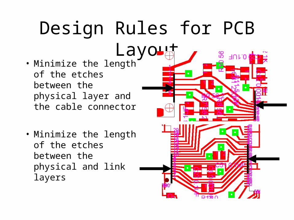
Design Rules for PCB Layout• Minimize the length
of the etches between the physical layer and the cable connector
• Minimize the length of the etches between the physical and link layers
Design Rules for PCB Layout
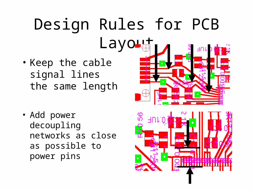
• Keep the cable signal lines the same length
• Add power decoupling networks as close as possible to power pins
Design Rules for PCB Layout
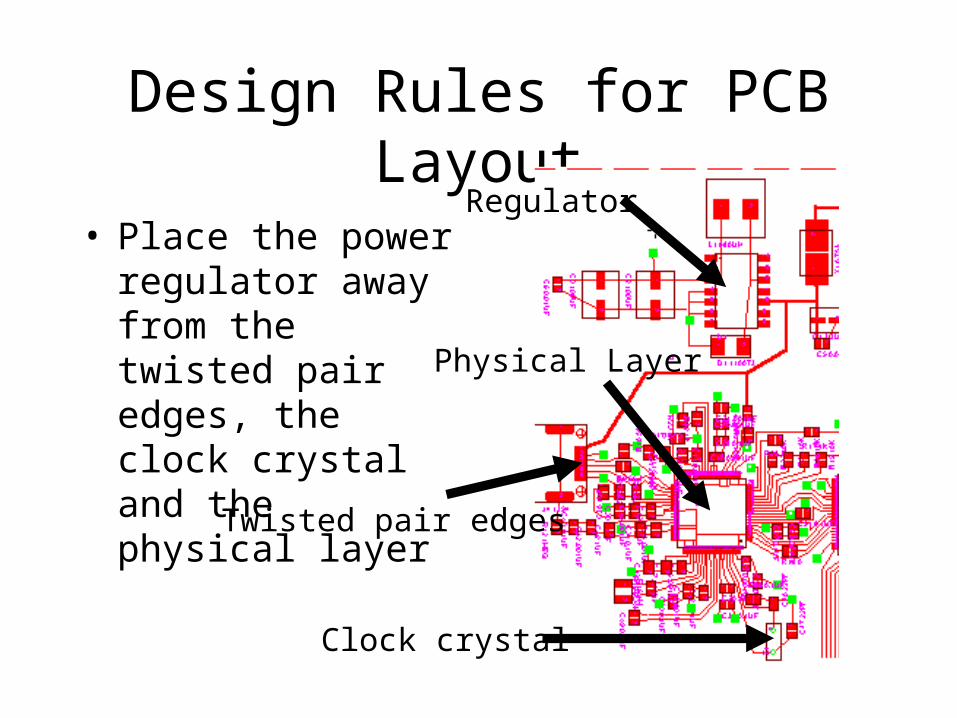
• Place the power regulator away from the twisted pair edges, the clock crystal and the physical layer
Regulator
Physical Layer
Twisted pair edges
Clock crystal
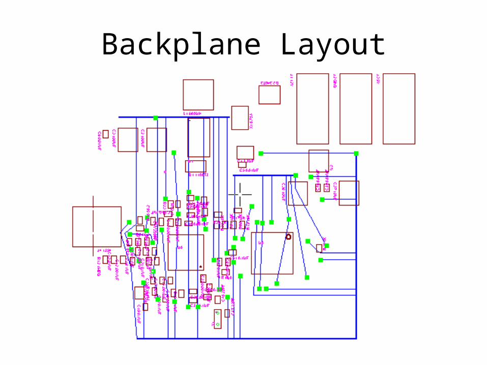
Backplane Layout
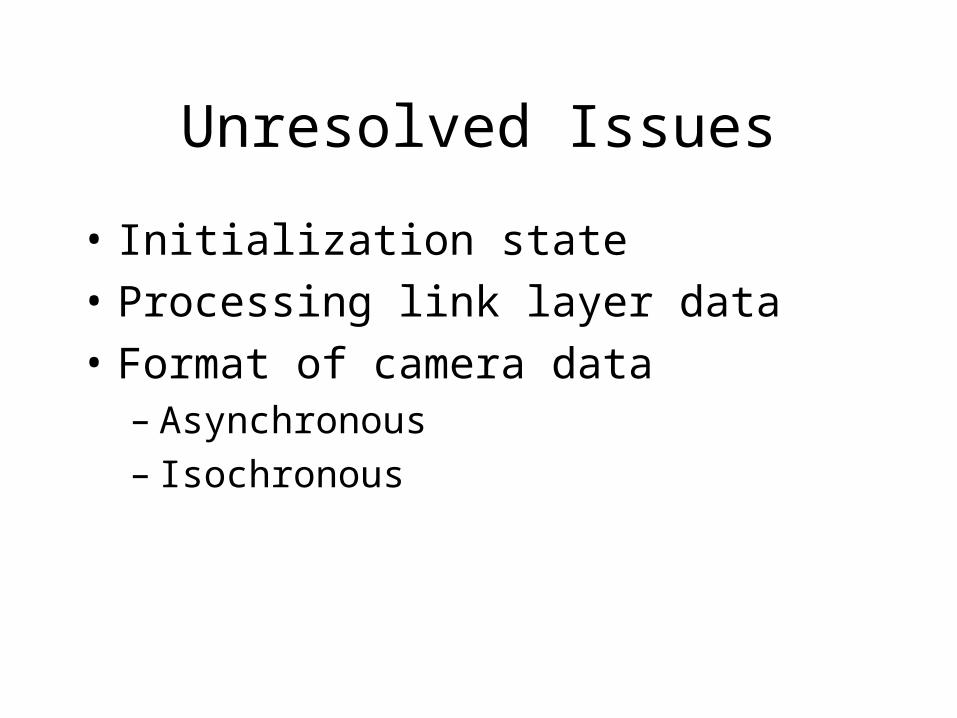
Unresolved Issues
• Initialization state
• Processing link layer data
• Format of camera data– Asynchronous– Isochronous

Upcoming Milestones
• Board fabrication
• Testing
• Determination of initialization state
• Transmission of data


