IEEE COMMUNICATIONS SURVEYS & TUTORIALS, VOL. 14, NO. 4, FOURTH QUARTER 2012 1021 A Survey on Optical Interconnects for Data Centers Christoforos Kachris and Ioannis Tomkos Abstract—Data centers are experiencing an exponential in- crease in the amount of network traffic that they have to sustain due to cloud computing and several emerging web applications. To face this network load, large data centers are required with thousands of servers interconnected with high bandwidth switches. Current data center networks, based on electronic packet switches, consume excessive power to handle the increased communication bandwidth of emerging applications. Optical interconnects have gained attention recently as a promising solution offering high throughput, low latency and reduced energy consumption compared to current networks based on commodity switches. This paper presents a thorough survey on optical interconnects for next generation data center networks. Furthermore, the paper provides a qualitative categorization and comparison of the proposed schemes based on their main features such as connectivity and scalability. Finally, the paper discusses the cost and the power consumption of these schemes that are of primary importance in the future data center networks. Index Terms—Optical interconnects, data center networks. I. I NTRODUCTION O VER the last few years, the exponential increase of the Internet traffic, mainly driven from emerging applica- tions like streaming video, social networking and cloud com- puting has created the need for more powerful data centers. The applications that are hosted in the data center servers (e.g. cloud computing applications, search engines, etc.) are data-intensive and require high interaction between the servers in the data center [1]. This required interaction poses a significant challenge to the networking of the data centers creating the need for more efficient interconnection schemes with high bandwidth and reduced latency. The servers must experience low latency communication among each other, even if the data center continue to increase in size comprising thousand of servers. However, while the throughput and the latency in the future data center networks must be improved significantly to sustain the increased network traffic, the total power consumption inside the racks must remain almost the same due to thermal constraints [2]. Furthermore, as more and more processing cores are in- tegrated into a single chip, the communication requirements between racks in the data centers will keep increasing sig- nificantly [3]. Table I shows the projections for performance, bandwidth requirements and power consumption for the future high performance systems [4],[5]. Note that while the peak performance will continue to increase rapidly, the budget for the total allowable power consumption that can be afforded by Manuscript received 5 May 2011; revised 30 August 2011, 25 November 2011, and 1 December 2011. C. Kachris is with Athens Information Technology, Athens, Greece (e-mail: [email protected]). I. Tomkos is a professor at Athens Information Technology, Athens, Greece. Digital Object Identifier 10.1109/SURV.2011.122111.00069 TABLE I PERFORMANCE, BW REQUIREMENTS AND POWER CONSUMPTION BOUND FOR FUTURE SYSTEMS [4],[5] Year Peak Performance (10x/4 yrs) Bandwidth requirements (20x/4 yrs) Power consump- tion bound (2x/4 yrs) 2012 10 PF 1 PB/s 5 MW 2016 100 PF 20 PB/s 10 MW 2020 1000 PF 400 PB/s 20 MW the data center is increasing in a much slower rate (2x every 4 years) due to several thermal dissipation issues. Therefore one of the most challenging issues in the design and deployment of a data center is the power consumption. The energy consumption of the data center infrastructures and the Internet network topology [6],[7] are the ones that mainly define the overall energy consumption of cloud computing. Greenpeace’s Make IT Green report [8], estimates that the global demand for electricity from data centers was around 330bn kWh in 2007. This demand is projected to triple by 2020 (more than 1000bn kWh). According to some estimates [9], the power consumption of the data centers in the US in 2006 was 1.5% of the total energy consumed at a cost of more than $4.5B. The servers in the data centers consume around 40% of the total IT power, storage up to 37% and the network devices consume around 23% of the total IT power [10]. And as the total power consumption of IT devices in the data centers continues to increase rapidly, so does the power consumption of the HVAC equipment (Heating-Ventilation and Air-Conditioning) to keep steady the temperature of the data center site. Therefore, the reduction in the power consumption of the network devices has a significant impact on the overall power consumption of the data center site. The power consumption of the data centers has also a major impact on the environment. In 2007, data centers accounted for 14% of the total ICT greenhouse gases (GHG) emissions (or 2% of the global GHG), and it is expected to grow up to 18% by 2020 [11]. The global data center footprint in greenhouse gases emissions was 116 Metric Tonne Carbon Dioxide (MtCO 2 e) in 2007 and this is expected to more than double by 2020 to 257 MtCO 2 e, making it the fastest- growing contributor to the ICT sectors carbon footprint. In order to face this increased communication bandwidth demand and the power consumption in the data centers, new interconnection schemes must be developed that can provide high throughput, reduced latency and low power consumption. Optical networks have been widely used in the last years in the long-haul telecommunication networks, providing high throughput, low latency and low power consumption. Several schemes have been presented for the exploitation of the light’s 1553-877X/12/$31.00 c 2012 IEEE
A Survey on Optical Interconnects for Data CentersChristoforos Kachris and Ioannis Tomkos
Abstract—Data centers are experiencing an exponential in-crease in the amount of network traffic that they have to sustaindue to cloud computing and several emerging web applications.To face this network load, large data centers are requiredwith thousands of servers interconnected with high bandwidthswitches. Current data center networks, based on electronicpacket switches, consume excessive power to handle the increasedcommunication bandwidth of emerging applications. Opticalinterconnects have gained attention recently as a promisingsolution offering high throughput, low latency and reducedenergy consumption compared to current networks based oncommodity switches. This paper presents a thorough survey onoptical interconnects for next generation data center networks.Furthermore, the paper provides a qualitative categorization andcomparison of the proposed schemes based on their main featuressuch as connectivity and scalability. Finally, the paper discussesthe cost and the power consumption of these schemes that areof primary importance in the future data center networks.
Index Terms—Optical interconnects, data center networks.
I. INTRODUCTION
OVER the last few years, the exponential increase of theInternet traffic, mainly driven from emerging applica-
tions like streaming video, social networking and cloud com-puting has created the need for more powerful data centers.The applications that are hosted in the data center servers(e.g. cloud computing applications, search engines, etc.) aredata-intensive and require high interaction between the serversin the data center [1]. This required interaction poses asignificant challenge to the networking of the data centerscreating the need for more efficient interconnection schemeswith high bandwidth and reduced latency. The servers mustexperience low latency communication among each other,even if the data center continue to increase in size comprisingthousand of servers. However, while the throughput and thelatency in the future data center networks must be improvedsignificantly to sustain the increased network traffic, the totalpower consumption inside the racks must remain almost thesame due to thermal constraints [2].
Furthermore, as more and more processing cores are in-tegrated into a single chip, the communication requirementsbetween racks in the data centers will keep increasing sig-nificantly [3]. Table I shows the projections for performance,bandwidth requirements and power consumption for the futurehigh performance systems [4],[5]. Note that while the peakperformance will continue to increase rapidly, the budget forthe total allowable power consumption that can be afforded by
Manuscript received 5 May 2011; revised 30 August 2011, 25 November2011, and 1 December 2011.
C. Kachris is with Athens Information Technology, Athens, Greece (e-mail:[email protected]).
I. Tomkos is a professor at Athens Information Technology, Athens, Greece.Digital Object Identifier 10.1109/SURV.2011.122111.00069
TABLE IPERFORMANCE, BW REQUIREMENTS AND POWER CONSUMPTION BOUND
FOR FUTURE SYSTEMS [4],[5]
Year PeakPerformance(10x/4 yrs)
Bandwidthrequirements(20x/4 yrs)
Power consump-tion bound (2x/4yrs)
2012 10 PF 1 PB/s 5 MW2016 100 PF 20 PB/s 10 MW
2020 1000 PF 400 PB/s 20 MW
the data center is increasing in a much slower rate (2x every4 years) due to several thermal dissipation issues.
Therefore one of the most challenging issues in the designand deployment of a data center is the power consumption.The energy consumption of the data center infrastructures andthe Internet network topology [6],[7] are the ones that mainlydefine the overall energy consumption of cloud computing.Greenpeace’s Make IT Green report [8], estimates that theglobal demand for electricity from data centers was around330bn kWh in 2007. This demand is projected to triple by2020 (more than 1000bn kWh). According to some estimates[9], the power consumption of the data centers in the US in2006 was 1.5% of the total energy consumed at a cost ofmore than $4.5B. The servers in the data centers consumearound 40% of the total IT power, storage up to 37% and thenetwork devices consume around 23% of the total IT power[10]. And as the total power consumption of IT devices in thedata centers continues to increase rapidly, so does the powerconsumption of the HVAC equipment (Heating-Ventilationand Air-Conditioning) to keep steady the temperature ofthe data center site. Therefore, the reduction in the powerconsumption of the network devices has a significant impacton the overall power consumption of the data center site.
The power consumption of the data centers has also a majorimpact on the environment. In 2007, data centers accountedfor 14% of the total ICT greenhouse gases (GHG) emissions(or 2% of the global GHG), and it is expected to grow upto 18% by 2020 [11]. The global data center footprint ingreenhouse gases emissions was 116 Metric Tonne CarbonDioxide (MtCO2e) in 2007 and this is expected to morethan double by 2020 to 257 MtCO2e, making it the fastest-growing contributor to the ICT sectors carbon footprint.
In order to face this increased communication bandwidthdemand and the power consumption in the data centers, newinterconnection schemes must be developed that can providehigh throughput, reduced latency and low power consumption.Optical networks have been widely used in the last yearsin the long-haul telecommunication networks, providing highthroughput, low latency and low power consumption. Severalschemes have been presented for the exploitation of the light’s
high bandwidth such as Time Division Multiplexing (TDM)and Wavelength Division Multiplexing (WDM). In the case ofWDM, the data are multiplexed using separate wavelength thatcan traverse simultaneously in the fiber providing significantlyhigher bandwidth. The optical telecommunication networkshave evolved from traditional opaque networks toward all-optical (i.e. transparent) networks. In opaque networks, theoptical signal carrying traffic undergoes an optical-electronic-optical (OEO) conversion at every routing node. But as thesize of opaque networks increases, network designers hadto face several issues such as higher cost, heat dissipation,power consumption, and operation and maintenance cost. Onthe other hand, all-optical networks provide higher bandwidth,reduced power consumption and reduced operation cost usingoptical cross-connects and reconfigurable optical add/dropmultiplexers (ROADM) [12].
Currently the optical technology is utilized in data centersonly for point-to-point links in the same way as point-to-pointoptical links were used in older telecommunication networks(opaque networks). These links are based on low cost multi-mode fibers (MMF) for short-reach communication. TheseMMF links are used for the connections of the switchesusing fiber-based Small Form-factor Pluggable transceivers(SFP for 1 Gbps and SFP+ for 10 Gbps) displacing thecopper-based cables [13]. In the near future higher bandwidthtransceivers are going to be adopted (for 40 Gbps and 100Gbps Ethernet) such as 4x10 Gbps QSFP modules with four10 Gbps parallel optical channels and CXP modules with 12parallel 10 Gbps channels. The main drawback in this case isthat power hungry electrical-to-optical (E/O) and optical-to-electrical (O/E) transceivers are required since the switchingis performed using electronic packet switches.
Current telecommunication networks are using transparentoptical networks in which the switching is performed at theoptical domain to face the high communication bandwidth.Similarly, as the traffic requirements in data centers areincreasing to Tbps, all-optical interconnects (in which theswitching is performed at the optical domain) could providea viable solution to these systems that will meet the hightraffic requirements while decreasing significantly the powerconsumption [14],[15],[16]. According to a report, all-opticalnetworks could provide up to 75% energy savings in thedata centers [17]. Especially in large data centers used inenterprises the use of power efficient, high bandwidth and lowlatency interconnects is of paramount importance and there issignificant interest in the deployment of optical interconnectsin these data centers [18].
A. Current DC with commodity switches
Figure 1 shows the high level block diagram of a typicaldata center. A data center consists of multiple racks hosting theservers (e.g. web, application or database servers) connectedthrough the data center interconnection network. When arequest is issued by a user, then a packet is forwarded throughthe Internet to the front end of the data center. In the frontend, the content switches and the load balance devices areused to route the request to the appropriate server. A requestmay require the communication of this server with many other
servers. For example, a simple web search request may requirethe communication and synchronization between the web, theapplication and the database servers.
Most of the current data centers are based on commodityswitches for the interconnection network. The network isusually a canonical fat-tree 2-Tier or 3-Tier architecture asit is depicted in Figure 1 [19]. The servers (usually up to 48in the form of blades) are accommodated into racks and areconnected through a Top-of-the-Rack Switch (ToR) using 1Gbps links. These ToR switches are further inter-connectedthrough aggregate switches using 10 Gbps links in a treetopology. In the 3-Tier topologies (shown in the figure) onemore level is applied in which the aggregate switches areconnected in a fat-tree topology using the core switches eitherat 10 Gbps or 100 Gbps links (using a bundle of 10 Gbps links)[20]. The main advantage of this architecture is that it can bescaled easily and that it is fault tolerant (e.g. a ToR switch isusually connected to 2 or more aggregate switches).
However, the main drawback of these architectures is thehigh power consumption of the ToR, aggregate and coreswitches (due to O/E and E/O transceivers and the electronicswitch fabrics) and the high number of links that are re-quired. Another problem of the current data center networksis the latency introduced due to multiple store-and-forwardprocessing [21]. When a packet travels from one server toanother through the ToR, the aggregate and the core switch,it experiences significant queuing and processing delay ineach switch. As the data centers continue to increase to facethe emerging web applications and cloud computing, moreefficient interconnection schemes are required that can providehigh throughput, low latency and reduced energy consumption.While there are several research efforts that try to increasethe required bandwidth of the data centers that are based oncommodity switches (e.g. using modified TCP or Ethernetenhancements [22]), the overall improvements are constraintsby the bottlenecks of the current technology.
B. Organization of the paper
This paper presents a thorough survey of the optical in-terconnect schemes for data centers that have been recentlypresented in the research literature. The paper presents bothhybrid and all-optical schemes based either on optical circuitswitching or on packet/burst switching. Section II presentsthe network traffic characteristics of the data center networks.Section III presents the optical technology and the componentsthat are used in the design of optical interconnects. SectionIV presents the architectures of the optical interconnectsand discusses the major features of each scheme. Section Vpresents a qualitative comparison and categorization of theseschemes. Finally, Section VI discusses the issues of cost andpower consumption in these networks and Section VII presentsthe conclusions. In summary the main contributions of thispaper are the followings:
• Survey of the optical networks targeting data centers andinsight behind these architectures
• Categorization and qualitative comparison of the pro-posed schemes based on the technology, connection type,architecture, etc.
KACHRIS and TOMKOS: A SURVEY ON OPTICAL INTERCONNECTS FOR DATA CENTERS 1023
…ToRswitches
AggregateSwitches
10 Gbps
Rack
Coreswitches
Servers
Internet
Data Center Clients
Rack Rack Rack
10 Gbps
Data Center
Content switches &Load balance
Fig. 1. Architecture of current data center network
• Analysis of optical interconnect’s benefits in terms ofpower consumption and cost
II. NETWORK TRAFFIC CHARACTERISTICS
In order to design a high performance network for a datacenter, a clear understanding of the data center traffic char-acteristics is required. This section presents the main featuresof the network traffic in the data centers and discusses howthese features affect the design of the optical networks. Thereare several research papers that have investigated the datacenter traffic such as the ones presented by Microsoft Research([23],[24],[25]). The data centers can be categorized in threeclasses: university campus data centers, private enterprise datacenters and cloud-computing data centers. In some casesthere are some common traffic characteristics (e.g. averagepacket size) in all data centers while other characteristics (e.g.applications and traffic flow) are quite different between thedata center categories. The results presented in these papers arebased on measurement of real data centers. Until now there isnot any study on a theoretical model of the data center traffic.However, based on these studies we can extract some usefulfigures of merit for the modeling of the data center traffic. Forexample the interarrival rate distribution of the packet in the
in the private data centers follows the lognormal distributionwhile the campus data center follows the weibull distribution[25].
The main empirical findings of these studies are the follow-ings:
• Applications: The applications that are running on thedata centers depend on the data center category. Incampus data centers the majority of the traffic is HTTPtraffic. On the other hand, in private data centers andin data centers used for cloud computing the traffic isdominated by HTTP, HTTPS, LDAP, and DataBase (e.g.MapReduce) traffic.
• Traffic flow locality: A traffic flow is specified as anestablished link (usually TCP) between two servers. Thetraffic flow locality describes if the traffic generated bythe servers in a rack is directed to the same rack (intra-rack traffic) or if it directed to other racks (inter-rack traf-fic). According to these studies the traffic flow ratio forinter-rack traffic fluctuates from 10% to 80% dependingon the application. Specifically, in data centers used byeducational organization and private enterprises the ratioof intra-rack traffic ranges from 10% to 40%. On the otherhand, in data centers that are used for cloud computingthe majority of the traffic is intra-rack communication(up to 80%). The operators in these systems locatethe servers, that usually exchange high traffic betweeneach other, into the same rack. The traffic flow localityaffects significantly the design of the network topology.In cases of high inter-rack communication traffic, highspeed networks are required between the racks while low-cost commodity switches can be used inside the rack.Therefore, in these cases an efficient optical networkcould provide the required bandwidth demand betweenthe racks while low cost electronic switches can beutilized for intra-rack communication.
• Traffic flow size and duration: A traffic flow is definedas an active connection between 2 or more servers. Mosttraffic flow sizes in the data center are considerably small(i.e. less than 10KB) and a significant fraction of theseflows last under a few hundreds of milliseconds. The du-ration of a traffic flow can affect significantly the designof the optical topology. If the traffic flow lasts severalseconds then an optical device with high reconfigurationtime can sustain the reconfiguration overhead in order toprovide higher bandwidth.
• Concurrent traffic flows: The number of concurrent traf-fic flows per server is also very important to the design ofthe network topology. If the number of concurrent flowscan be supported by the number of optical connectionsthen optical networks can provide significant advantageover the networks based on electronic switches. Theaverage number of concurrent flows is around 10 in themajority of the data centers servers.
• Packet size: The packet size in data centers exhibit abimodal pattern with most packet sizes clustering around200 and 1400 bytes. This is due to the fact that thepackets are either small control packets or are parts oflarge files that are fragmented to the maximum packetsize of the Ethernet networks (1550 bytes).
• Link utilization: According to these studies, in all kindsof data centers the link utilization inside the rack and inthe aggregate level is quite low, while the utilization onthe core level is quite high. Inside the rack the preferabledata rate links are 1 Gbps (in some cases each rack serverhosts 2 or more 1 Gbps links), while in the aggregateand in the core network, 10 Gbps are usually deployed.The link utilization shows that higher bandwidth links arerequired especially in the core network, while the current1 Gbps Ethernet networks inside the rack can sustain thefuture network demands.
III. OPTICAL TECHNOLOGY
The majority of the optical interconnections schemes pre-sented in this paper are based on devices that are widely usedin optical telecommunication networks (e.g. WDM networksand Passive optical networks (PONs)). This section describesthe basic optical modules that are utilized for the implemen-tation of the optical interconnects targeting data centers [26].
• Splitter and combiner: A fiber optic splitter is a passivedevice that can distribute the optical signal (power) fromone fiber among two or more fibers. A combiner on theother hand is used to combine optical signal from two ormore fibers into a single fiber.
• Coupler: A coupler is a passive device that is used tocombine and split signals in an optical network but canhave multiple inputs and outputs. For example, a 2x2coupler takes a fraction of the power from the first inputand places it on output 1 and the remaining fraction onoutput 2 (similarly for the second input).
• Arrayed-Waveguide Grating (AWG): AWGs are pas-sive data-rate independent optical devices that route eachwavelength of an input to a different output (wavelengthw of input i is routed to output [( i + w - 2) mod N]+1,1 ≤ i ≤ N , 1 ≤ w ≤ W , where N is the number ofports and W the total number of wavelengths). In WDMcommunication systems where multiple wavelength aremultiplexed, AWGs are used as demultiplexers to sep-arate the individual wavelengths or as multiplexers tocombine them.
• Wavelength Selective Switch (WSS): A WSS is typicalan 1xN optical component than can partition the incom-ing set of wavelengths to different ports (each wavelengthcan be assigned to be routed to different port). In otherwords, WSS can be considered as reconfigurable AWGand the reconfiguration time is a few milliseconds [27].
• Micro-Electro-Mechanical Systems Switches (MEMS-switches): MEMS optical switches are mechanical de-vices that physically rotate mirror arrays redirecting thelaser beam to establish a connection between the inputand the output. Because they are based on mechanicalsystems the reconfiguration time is in the orders of afew milliseconds. Currently that are commercial availableMEMS optical switches with 32 input/output ports.
• Semiconductor Optical Amplifier (SOA): Semiconduc-tor Optical Amplifiers are optical amplifiers that arebased on silicon p-n junctions. Light is amplified throughstimulated emission when it propagates through the active
region [28]. SOAs are generally preferred over otheramplifiers due to their fast switching time (in the orderof ns) and their energy efficiency [29].
• Tunable Wavelength Converters (TWC): A tunablewavelength converter generates a configurable wave-length for an incoming optical signal. The tunable wave-length converter includes a tunable laser, a SOA and aMach-Zehnder Interferometer (MZI). The conversion isperformed by the SOA which receives as an input thetunable laser wavelength and the data and outputs thedata in the selected wavelength. The SOA is followed bythe MZI which works as a filter to generate reshaped andclean pulses of the tuned wavelength [30],[31]. In [32] itis shown that the wavelength conversion can be achievedat 160 Gbps and the reconfiguration time is in the orderof nanoseconds.
IV. ARCHITECTURES
This section presents the optical interconnects schemes thathave been recently proposed for data center networks andprovides a general insight on each architecture.
A. c-Through: Part-time optics in data centers
A hybrid electrical-optical network has been presented byG. Wang et al. called c-Through [33],[34]. The architectureof c-Through is depicted in Figure 2 and is presented asan enhancement to the current data center networks. TheToR switches are connected both to an electrical packet-based network (i.e. Ethernet) and an optical circuit-basednetwork. The circuit switch network can only provide amatching on the graph of racks. Thus the optical switchmust be configured in a way that pairs of rack with highbandwidth demands are connected through this optical switch.A traffic monitoring system is required which is placed in thehosts and it measures the bandwidth requirements with theother hosts. An optical configuration manager collects thesemeasurements and determines the configuration of the opticalswitch based on the traffic demands. The traffic demand andthe connected links are formulated as a maximum weightperfect matching problem. In the c-Through architecture theEdmonds’ algorithms has been used for the solution of theperfect matching algorithm [35].
After the configuration of the optical circuit switch, theoptical manager informs the ToR switches in order to routethe packets accordingly. The traffic in the ToR switches is de-multiplexed by using a VLAN-based routing. Two differentVLANs are used, one for the packet based network and one forthe optical circuit based network. If the packets are destined toa ToR switch that is connected to the source ToR through theoptical circuit, the packets are destined to the second VLAN.
The system evaluation was based on simulation of a packet-switch network. The proposed scheme was evaluated usingboth micro-benchmarks and real applications. In the evaluationit was shown that for applications in which the traffic demandbetween some hosts changes slowly, the proposed scheme canreduce significantly the completion time of the applicationsand offers significantly reduced latency between the nodesconnected through the optical circuit.
KACHRIS and TOMKOS: A SURVEY ON OPTICAL INTERCONNECTS FOR DATA CENTERS 1025
ToR
AggregateSwitch
CoreSwitch
Optical circuit switch
Fig. 2. Architecture of the c-Through network
B. Helios: A hybrid optical electrical switch
N. Farrington et al. from UCSD, presented in 2010 a hybridelectrical/optical switch architecture for modular data centerscalled Helios [36] that is similar to the c-Through architecturebut it is based on WDM links. Helios scheme follows thearchitecture of typical 2-layer data center networks. It consistsof ToR switches (called pod switches) and core switches. Podswitches are common electrical packet switches, while coreswitches can be either electrical packet switches or opticalcircuit switches. The electrical packet switches are used forall-to-all communication of the pod switches, while the opticalcircuit switches are used for high bandwidth slowly changing(usually long lived) communication between the pod switches.Hence, the Helios architecture tries to combine the best of theoptical and the electrical networks.
The high level architecture of the Helios architecture isdepicted in Figure 3. Each pod switch has both colorless andWDM optical transceivers. The colorless optical transceivers(e.g. 10G SFP+ modules) are used to connect the pod switcheswith the core electrical packet switches. The WDM opticaltransceivers are multiplexed through a passive optical multi-plexer (forming superlinks) and are connected to the opticalcircuit switches. These superlinks can carry up to w x 10 Gbps(where w is the number of wavelengths; from 1 to 32). Thusthe proposed scheme can deliver full bisection bandwidth. Ifthe number of colorless and WDM transceivers is the samethen the 50% of the bandwidth is shared between pods whilethe remaining 50% is allocated to specific routes dependingon the traffic requirements.
The Helios control scheme consists of three modules: theTopology Manager (TM), the circuit switch Manager (CSM)and the Pod Switch Manager (PSM). The topology manager isused to monitor the traffic of the data center and is based on thetraffic requirements (e.g. number of active connections, trafficdemand, etc.) to find the best configuration for the opticalcircuit switch. The traffic demand is based on the traffic thateach server needs to transmit to the other servers, while thenumber of active flows is the maximum number of connectionthat can be simultaneously active. The Circuit Switch Manager
ToR switches (pod switches)
10 Gbps linkWDM optical link
Electrical Packet switches Optical circuit switch
Fig. 3. Architecture of the Helios data center network
is used to receive the graph of the connections and to configurethe Glimmerglass MEMS switch. The Pod Switch Manageris hosted in the pod switches and is interfacing with theTM. Based on the configuration decisions on TM, the podmanager is used to route the packet either to the packet switchthrough the colorless transceivers or to the optical circuitswitch through the WDM transceivers. The configuration ofthe circuit switch is based on a simple demand matrix in whichthe bipartite graph has to be calculated.
The main advantage of the Helios architecture is that it isbased on readily available optical modules and transceiversthat are widely used in optical telecommunication networks.The optical circuit switch is based on the commerciallyavailable Glimmerglass switch and the pod switches use WDMSFP+ optical transceivers. The WDM transceivers can beeither Coarse WDM (CWDM) modules that are less expensivebut support a limited number of wavelengths or Dense WDM(DWDM) that are more expensive but can support highernumber of wavelengths (e.g. 40) since they use narrowerchannel spacing. For the performance evaluation they usedthe Glimmerglass crossbar optical circuit switch that is readilyavailable and can support up to 64 ports [37].
The main drawback of the proposed scheme is that it isbased on MEMS switches hence any reconfiguration of thecircuit switch requires several milliseconds (for the Glim-merglass switch the reconfiguration time was 25 ms). Thus,this scheme is ideal for applications where the connectionsbetween some nodes last more than a couple of secondsin order to compensate the reconfiguration overhead. In theperformance evaluation it was shown that when the stabilityparameter was varied from 0.5 to 16 seconds the throughputwas increased significantly.
C. DOS: A scalable optical switch
X. Ye et al. from University of California, Davis presentedin 2010 the DOS scalable Datacenter Optical Switch [38].The switching in the DOS architecture is based on ArrayedWaveguide Grating Router (AWGR) that allows contentionresolution in the wavelength domain. The cyclic wavelength
routing characteristics of the AWGR (presented in Section III)is exploited, that allows different inputs to reach the sameoutput simultaneously. Figure 4 depicts the high level blockdiagram of the DOS architectures.
The optical switch fabric consists of an array of tunablewavelength converters (one TWC for each node), an AWGRand a loopback shared buffer. Each node can access anyother node through the AWGR by configuring the transmittingwavelength of the TWC. The switch fabric is configured by thecontrol plane that controls the TWC and the label extractors(LEs). The control plane is used for the contention resolutionand TWC tuning. When a node transmits a packet to theswitch, the label extractors are used to separate the label fromthe optical payload. The optical label is converted to electricalsignal by an O/E converted inside the control plane moduleand it is forwarded to the arbitration unit. The label includesboth the destination address and the packet length. This label isstored in the label processor and this processor sends a requestto the arbitration unit for content resolution. Based on thedecision by the arbitration unit, the control plane configuresthe TWC. Hence based on the AWGR routing characteristics,the transmitted packet arrives to the destined output.
In case that the number of output receivers is less thanthe number of nodes that want to transmit to this port a linkcontention happens. In this case, a shared SDRAM bufferis used to store temporarily the transmitted packets. Thewavelengths that face the contention are routed to the SDRAMthrough a optical-electrical (O/E) converter. The packets arethen stored in SDRAM and a Shared buffer controller is usedto handle these packets. This controller sends the requests ofthe buffered packets to the control plane and waits for a grant.When the grant is received, the packet is retrieved from theSDRAM, then it is converted back to optical signal throughan electrical-optical converter and then it is forwarded to theswitch fabric through a TWC.
The main challenge is the deployment of the DOS switchis the arbitration of the requests in the control plane. Since,there are not used virtual output queues (VOQ), every inputissues a request to the arbiter and waits for the grant. Thus,for the scheduling of the packets a 2-phase arbiter can beused ([39]).The first phase is used for the arbitration of therequests and the second phase for the arbitration of the grants.Furthermore, since there are no virtual output queues only onerequest per output is issued. Thus a single iteration can be usedinstead of multiple iterations. However, the arbitration must becompleted in very short time since the DOS architecture is apacket-based switch.
The scalability of the DOS scheme depends on the scala-bility of the AWGR and the tuning range of the TWC. Someresearch centers have presented AWGR that can reach up to400 ports [40]. Thus the DOS architecture can be used toconnect up to 512 nodes (or 512 racks assuming that each nodeis used as a ToR switch). Although, many data centers utilizemore than 512 ToR switches, the DOS architecture could beeasily scaled up in a fat-tree topology (i.e. the optical switchcould be used for the aggregation layer).
The main advantage of the DOS scheme is that the latency isalmost independent of the number of input ports and remainslow even at high input loads. This is due to the fact that the
ControlPlane
ToRswitches
…
TWC
TWC
LE
LE
SDRAMBuffer
O/EO/E
O/EO/E
O/EO/E
O/EO/E
AWGRTWCLE
TWC
BufferO/EO/EO/EO/E
Controller
Fig. 4. DOS architecture
packets have to traverse only through an optical switch andthey avoid the delay of the electrical switch’s buffers.
However the main drawback of the DOS scheme is that it isbased on electrical buffers for the congestion management us-ing power hungry electrical-to-optical and optical-to-electricalconverters, thus increasing the overall power consumptionand the packet latency. Furthermore, the DOS architectureuse tunable wavelength transceivers that are quite expensivecompared to commodity optical transceivers used in currentswitches. However, DOS remains an attractive candidate fordata center networks where the traffic pattern is bursty withhigh temporary peaks. The tunable wavelength converters havea switching time in the orders of a few ns. Thus the proposedscheme can be reconfigured to meet the traffic fluctuation oncontrary to the slow switching time of MEMS optical switches.
A 40 Gbps 8x8 prototype of the DOS architecture has beenrecently presented by UCD and NPRC [41]. The prototypeis based on an 8x8 200 GHz spacing AWGR and it also in-cludes four wavelength converters (WC) based on cross-phasemodulation (XPM) in a semiconductor optical amplifier Mach-Zehnder interferometer (SOA-MZI). The measured switchinglatency of the DOS prototype was only 118.2 ns which ismuch lower compared to the latency of legacy data centers(i.e. in the order of few microseconds).
D. Proteus data center network
Proteus [42][43] is an all-optical architecture that is basedon WSS switch modules and an optical switching matrix that isbased on MEMS. The high level block diagram of the Proteusarchitecture is depicted in Figure 5. Each ToR switch hasseveral optical transceivers operating at different wavelengths.The optical wavelengths are combined using a multiplexer andare routed to a WSS. The WSS multiplex each wavelengthto up to k different groups and each group in connected toa port in the MEMS optical switch. Thus a point-to-point
KACHRIS and TOMKOS: A SURVEY ON OPTICAL INTERCONNECTS FOR DATA CENTERS 1027
connection is established between the ToR switches. On thereceiver’s path, all of the wavelengths are de-multiplexed androuted to the optical transceiver. The switching configurationof the MEMS determines which set of ToRs are connecteddirectly. In case that a TOR switch has to communicate witha ToR switch that is not directly connected, then it uses hop-by-hop communication. Thus Proteus must ensure that theentire ToR graph is connected when performing the MEMSreconfiguration.
The main idea of the Proteus project is to use direct opticalconnections between ToR switch for high-volume connectionswhile in case of low volume traffic to use multi-hop connec-tions. The main advantage of the Proteus project is that itcan achieve coarse-grain flexible bandwidth. Each ToR hasn optical transceivers. If for some reason the traffic betweentwo switches increase, then additional connections can be setup (up to n, either directly or indirectly) thus increasing theoptical bandwidth up to n times the bandwidth of one opticaltransceiver.
The main challenge in the operation of the Proteus networkis to find the optimum configuration for the MEMS switchfor each traffic pattern. In [42] an Integer Linear Programmingscheme is used to find the optimum configuration based on thetraffic requirements. The main advantage of the Proteus is thatit is based on readily available off-the-shelf optical modules(WSS such as the Finisar WSS [27], and optical multiplexers)that are widely used in optical telecommunication networksthus reducing the overall cost compared with ad-hoc solutions.
The main disadvantage of the Proteus architecture is thatthe MEMS switch reconfiguration time is in the order ofa few milliseconds. As it was discuss in Section II, themajority of the traffic flows last few milliseconds. Thus, inapplications where the traffic flow changes rapidly and eachserver establishes connection with other servers that last fewmilliseconds the proposed scheme cannot follow the trafficfluctuations. Hence, in many cases by the time the MEMSswitch is reconfigured, a new reconfiguration has to take placeto meet the new traffic demands. However, although the trafficbetween the servers changes rapidly the aggregated trafficbetween the ToR switches may change much slower. In thesecases, the Proteus scheme can exhibit high performance andreduced latency.
E. Petabit Optical SwitchJonathan Chao from Polytechnic Institute of New York has
presented a scalable bufferless optical switch fabric, calledPetabit switch fabric, that is based on AWGR and tunablewavelength converters [44],[45]. The proposed optical switchis combined efficiently with electronic buffering and schedul-ing. Figure 6 depicts the block diagram of the Petabit opticalswitch. The Petabit switch fabric adopts a three-stage Closnetwork and each stage consists of an array of AGWRs thatare used for the passive routing of packets. In the first stage,the tunable lasers are used to route the packets through theAWGRs, while in the second and in the third stage TWCare used to convert the wavelength and route accordingly thepackets to destination port.
The main difference compared to the DOS architectureis that Petabit switch does not use any buffers inside the
TRX1TRX2
WSS
MUX
...
TRX3
ToR
TRXN
Coupler
DEM
UX
Optical
OpticalSwitchingMatrix
ToRTRX1 p
Mux/Demux &Switching
OpticalMux/Demux &
Switching
ToRTRXN
...
TRX1
TRXN
...
Fig. 5. Proteus architecture
switch fabric (thus avoiding the power hungry E/O and O/Econversion). Instead, the congestion management is performedusing electronic buffers in the Line cards and an efficientscheduling algorithm. Each line card that is connected to theinput port of the Petabit switch hosts a buffer in which thepacket are stored before the transmission. The packets areclassified to different virtual output queues (VOQ) based onthe destination address. Given the high number of ports, aVOQ is maintained per OM (the last stage of the switch fabric)instead of one VOQ per output port. Using one VOQ per OMsimplifies the scheduling algorithm and the buffer managementbut on the other hand it introduced Head-of-line blocking(HOL). However, using an efficient scheduling algorithm andsome speedup, the Petabit switch fabric can achieve 100%throughput. The scheduler is used to find a bipartite matchfrom the input port to the output port and to assign a CM(the central stage of the switch fabric) for each match. Usingthe bipartite match scheduling, there is no congestion of thepackets in the switch fabric thus the buffer that is used in otherschemes (e.g. in the DOS architecture) is eliminated.
The performance evaluation of the Petabit switch is basedon a cycle-accurate frame-based simulator. The Petabit switchwas evaluated from 1024 to 10000 ports and it was shownthat it can achieve up to 99.6% throughput even in the case of10000 ports. The most important advantage of the proposedarchitecture is that the average latency is only twice of a frameduration (200 ns) even at 80% load using three iteration of thescheduling algorithm. Hence, in contrast to the current datacenter networks based on commodity switches, the latency issignificantly reduced and almost independent of the switchsize.
F. The OSMOSIS project
IBM and Corning jointly developed in 2004 the OSMOSISproject [46],[47] that is a low-latency optical broadcast-and-select (B&S) architecture based on wavelength- and space-division multiplexing. The broadcast-and-select architecture is
composed of two different stages. In the first stage, multiplewavelengths are multiplexed in a common WDM line and arebroadcasted to all the modules of the second stage through acoupler. The second stage use SOAs as fiber-selector gates toselect the wavelength that will be forwarded to the output.
In the framework of the OSMOSIS project, a 64-nodeinterconnect scheme has been developed, combining eightwavelengths on eight fibers to achieve 64-way distribution.The switching is achieved with a fast 8:1 fiber-selectionstage followed by a fast 8:1 wavelength-selection stage ateach output port as it is depicted in Figure 7. Rather thanusing tunable filters, this design features a demux-SOA-select-mux architecture. A programmable centralized arbitration unitreconfigures the optical switch via a separate optical centralscheduler synchronously with the arrival of fixed-length op-tical packets. The arbiter enables high-efficiency packet-levelswitching without aggregation or prior bandwidth reservationand achieves a high maximum throughput. The proposedscheme includes 64 input and output ports operating at 40Gbps. The main advantage of the proposed scheme is that theswitch can be scaled efficiently by deploying several switchesin a two-level (three-stage) fat tree topology. For example,it can be scaled up to 2048 nodes be deploying 96 64x64switches (64 switches for the first level and 32 switches forthe second level).
The line cards of the OSMOSIS architecture (that couldbe also interfaces of ToR switches) use distributed-feedback(DFB) laser for the transmitter which is coupled to a 40 Gbpselectro-absorption modulator (EAM). On the other hand, tworeceivers per port have been included in the input path. Thepresence of two receivers can be exploited by changing thearbiter to match up to two inputs to one output, instead of justone, which requires modifications to the matching algorithm.The main drawback of the proposed scheme is that it is basedon power hungry SOA devices, that increase significantly theoverall power consumption.
G. Space-Wavelength architecture
Castoldi et al. have presented an interconnection scheme fordata centers that is based on space-wavelength switching [48].The block diagram of the proposed architecture is depicted inFigure 8. In wavelength-switched architectures the switching isachieved by transmitting the packets on different wavelengths(using an array of fixed lasers or one fast tunable laser)
SOASOASOA
SOASOASOA
8x1 1x128ToR
Broadcast Select
SOASOASOASOASOASOA
SOASOASOASOASOASOA
...
OptAmp
... x8x128
...
Fig. 7. The OSMOSIS architecture
based on the destination ports. On the other hand, in space-switched architectures one fixed laser per port is requiredand a non-blocking optical switch based on SOA is used forthe establishment of the connections in each time slot. Theproposed scheme combines efficiently both the wavelengthand the space switching. Each node (e.g. server or ToR switch)has up to N ports and each port is connected through an intra-card scheduler to an array of fixed lasers, each one transmittingat different wavelength in the C-band (1530-1570nm). Eachlaser is connected to an electrical-to-optical transceiver andthese transceivers are connected to 1xM space switch. For thereception, each port is equipped with a fixed receiver, tunedon a specific wavelength.
To switch a packet from an input port to its output port, thedestination card is selected by setting the 1xM space switch,while its destination port on the card is selected by selectingthe wavelength to be modulated. The 1xM space switch fabricis composed by an array of SOAs forming a tree structure.
The scheduling problem consists in selecting a packet fromeach input port and placing it into a matrix representing thecard and port domains, so that no more than one packetcoming from the same card is present in each row. Each cardhas an inter-card scheduler that is used for the schedulingof the packets and the control of the optical transceivers.The proposed scheme can be scaled by adding more planes(wavelengths) thus increasing the aggregated bandwidth andreducing the communication latency. For example, up to 12channels (planes) can be accommodated using the C-band forthe fixed transceivers.
The main drawback of the proposed scheme is that theswitch fabric is based on SOA arrays that are expensiveand increase the overall power consumption. However, theperformance evaluation shows that the proposed scheme canachieve low latency even for high network utilization usingi.e. 12 separate planes.
H. E-RAPID
A. Kodi and A. Louri from University of Ohio and Univer-sity of Arizona respectively, have jointly presented an energy-efficient reconfigurable optical interconnects, called E-RAPID.This scheme can be used for high performance computingwhile it could be also deployed in data center networks [49].The high level block diagram of this scheme is depicted in
KACHRIS and TOMKOS: A SURVEY ON OPTICAL INTERCONNECTS FOR DATA CENTERS 1029
I t d
TX
Intra cardh d l
0
…
Blades or ToR
Inter cardScheduler
Card 1
SOA basedswitchfabric
scheduler
TX
n
RX
RX
Card 2
Card N
Fig. 8. The Space-wavelength architecture
Figure 9 (several modules such as buffers between the nodeshave been omitted for simplicity). Each module (i.e. rack)hosts several nodes (i.e. blade servers) and several transmittersthat are based on VCSEL lasers. A Reconfigurable controlleris used to control the crossbar switch and to allocate thenodes to a specific VCSEL laser. At any given time only oneVCSEL laser is active on each wavelength. A coupler for eachwavelength is used to select the VCSEL that will forwardthe packet to the Scalable Optical Remote Super Highwayring (SRS). This SRS highway is composed of several opticalrings; one for each rack. In the receiver path, an AWG isused for de-multiplexing of the wavelengths that are routedto an array of receivers. Then the crossbar switch is used toforward the packets from each receiver to the appropriate nodein the board. For example, if a server from Rack 0 needs tosend a packet to Rack 3, then the reconfigurable controllerconfigures the crossbar switch to connect the server with oneof the VCSEL lasers tuned at wavelength λ1. The VCSELis transmitting the packet using the second coupler that isconnected with the inner SRS ring (λ1). The inner SRS ringmultiplexes all the wavelengths that are destined to Rack 3. InRack 3 the AWG is used to demultiplex the wavelengths andthen route the packet to the server using the crossbar switch.
The E-RAPID can be dynamically reconfigured in the sensethat the transmitter ports can be reconfigured to different wave-lengths in order to reach different boards. In case of increasedtraffic loads, more wavelengths can be used for node-to-nodecommunication thus increasing the aggregate bandwidth ofthis link. In the control plane a static routing and wavelengthallocation (RWA) manager is used for the control of thetransmitters and the receivers. A Reconfigurable Controller(RC) is hosted in each module that controls the transmittersand the receivers of this module. The reconfigurable controlleris also used for the control of the crossbar switch that is usedto connect the nodes with the appropriate optical transceiver.
The main advantage of the E-RAPID architecture is thatthe power consumption can be adjusted based on the traffic
VCSEL
Coupler
Receivers
Transmitters
Crossbarswitch
ScalableOpticalRemoteSuperHighway(SRS)
VCSEL
VCSEL
VCSEL
PD
PD
PD
PD
0
1
2
3
ReconfigurableController
AWG
Rack 0
Rack 1
Rack 2
Rack 3
1
2
3
0, 1, 2, 3
Servers
Fig. 9. The E-RAPID architecture
load. E-RAPID is based on VCSEL transmitters in which thesupply current is adjusted based on the traffic load. When thetraffic load is reduced, the bit rate can be scaled down byreducing the supply voltage thus resulting power savings. Alock-step (LS) algorithm has been developed that can controlthe bit-rate (and the power saving) based on the networktraffic demands. Each node of the module sends a requestto the reconfigurable controller. The controller aggregates therequests and based on the traffic demand controls the VCSELthe crossbar switch, transmitter and the receivers. The perfor-mance evaluation shows that depending on the reconfigurationwindows (from 500 to 400 cycles) the latency of the packetsrange from less than 1 microsecond to 2 microseconds, thusproviding significantly lower latencies than networks based oncommodity switches.
I. The IRIS project
DARPA has also funded a research program called ”Data inthe Optical Domain-Networking” in which Alcatel-Lucent wasparticipating. The result of this project was the IRIS Project[50]. IRIS is also based on Wavelength Division Multiplexingand the characteristics on Arrayed Waveguide Grating Routers(AWGR) based on all optical wavelength converters. IRISarchitecture is based on a three-stage switch. The three-stagearchitecture is dynamically non-blocking even though the twospace switches are partially blocking. Each node (i.e. ToRswitch) is connected to a port of the first stage using N WDMwavelengths. The first stage consists of an array of wavelengthswitches (WS), and each wavelength switch is based on anarray of all-optical SOA-based wavelength converters that isused for the wavelength routing. The second stage is a timeswitch that consists of an array of optical time buffers. Thetime switch is composed of an array of WC and two AWGinterconnected with a number of optical lines, each one withdifferent delays. Based on the delay that needs to be added, theWC converts the optical signal to a specific wavelength thatis forwarded to the AWG with the required time delay. Thedelayed signals are multiplexed through a second AGW andare routed to the third stage (a second space switch). Basedon the final destination port, the signal is converted to therequired wavelength for the AWG routing.
WC: Wavelength converterWS: Wavelength SwitchHD: Header detectorTB: Time Buffer
Time Buffer
Fig. 10. The IRIS project
Due to the periodic operation of the third space switch,the scheduling is local and deterministic to each time bufferwhich greatly reduces control-plane complexity and removesthe need for optical random access memory. Using 40 Gb/sdata packets and 80x80 AWGs allows this architecture to scaleto 802x40 Gb/s = 256 Tb/s.
The IRIS project has been prototyped using 4 XFPtransceivers at 10 Gbps and has been implemented in an FPGAboard. A 40 Gb/s wavelength converter is used that is basedon fully-integrated circuit with a SOA for the wavelengthconversion [51]. The wavelengths conversion takes less than1ns. The conversion wavelength is either supplied internallyby an integrated fast-tunable multi-frequency laser (MFL) orexternally by a sampled-grating distributed Bragg reflector(SG-DBR) laser [51]. The optical switch is based on a passivesilica chip with dual 40x40 AWG.
J. Bidirectional photonic network
Bergman from Columbia University has presented an op-tical interconnection network for data networks based onbidirectional SOAs [52]. The proposed scheme is based onbidirectional SOA-based 2x2 switches that can be scaledefficiently in a tree-based topology as it is shown in Figure11. The nodes connected to this network can be either serverblades or ToR switches. Each of the switching nodes is a SOA-based 2x2 switch that consists of six SOAs. Each port canestablish any connection with the other ports in nanoseconds.The switching nodes are connected as a Banyan network(k-ary, n-trees) supporting kn processing nodes. The use ofbidirectional switches can provide significant advantages interms of component cost, power consumption, and footprintcompared to other SOA-based architectures like the broadcast-and-select architecture.
A prototype has been developed that shows the functionalityof the proposed scheme using 4 nodes at 40 Gbps [53]. Theoptical switching nodes are organized in a three-stage Omeganetwork with two nodes in each stage. The bit error rate thatwas achieved using four wavelengths was less than 10−12.The main advantage of this scheme is that it can be scaledefficiently to large number of nodes with reduced numberof optical modules, thus reduced power consumption. Thetotal number of nodes is only constrained by the congestionmanagement and the total required latency.
SOA
SOA
SOASOA SOA
SOA
Servers or ToR switchesServers or ToR switches
Fig. 11. The bidirectional switching node design
K. Data vortex
Bergman from Columbia University has also presenteda distributed interconnection network, called Data Vortex[54],[55]. Data vortex mainly targets high performance com-puting systems (HPC) but it can also be applied to data centerinterconnects [56]. The network consists of nodes that canroute both packet and circuit switched traffic simultaneouslyin a configurable manner based on semiconductor opticalamplifiers (SOA). The SOAs, organized in a gate-array config-uration, serve as photonic switching elements. The broadbandcapability of the SOA gates facilitates the organization ofthe transmitted data onto multiple optical channels. A 16node system has been developed in which the SOA array isdissected into subsets of four, with each group correspondingto one of the four input ports [57]. Similarly, one SOA gate ineach subset corresponds to one of four output ports, enablingnon-blocking operations of the switching node. Hence, thenumber of SOAs is quadruple the number of nodes (e.g. for32 nodes we would require 1024 SOAs).
The data vortex topology is composed entirely of 2x2switching elements arranged in a fully connected, directedgraph with terminal symmetry. The single-packet routingnodes are wholly distributed and require no centralized arbi-tration. The topology is divided into hierarchies or cylinders,which are analogous to the stages in a conventional banyannetwork as it is depicted in Figure 12.
The data vortex topology exhibits a modular architecturetherefore it can be scaled efficiently to large number of nodes.In all multistage interconnection networks, an important pa-rameter is the number of routing nodes a packet will traversebefore reaching its destination. For the data vortex that is basedon 2x2 switches, the number of intermediate nodes M scaleslogarithmically with the number of ports N as it is depictedbelow:M ≈ log2 N
The main drawback of the data vortex architecture is thatthe banyan multiple-stage scheme becomes extremely complex
KACHRIS and TOMKOS: A SURVEY ON OPTICAL INTERCONNECTS FOR DATA CENTERS 1031
SOANorth East
SouthWest
N d ( T R)Nodes (e.g. ToR)
Fig. 12. The data vortex architecture
when it is scaled to large networks. As the number of nodesincrease, the packets have to traverse several nodes beforereaching the destination address causing increased and non-deterministic latency.
L. Commercial optical interconnects
1) Polatis: While all of the above schemes are proposedby universities or industrial research centers there is alsoa commercial available optical interconnect for data centerthat is provided by Polatis Inc. The Polatis optical switchis based on piezo-electric optical circuit switching and beamsteering technology. Hence, the provided scheme is based ona centralized optical switch that can be reconfigured based onthe network traffic demand.
The most important feature of the provided switch is thelower power consumption (it is reported that the Polatis powerconsumption is only 45W compared to the 900+W of a legacydata center [58]), and it is data rate agnostic meaning that itcan support 10 Gbps, 40 Gbps and 100 Gbps. The only draw-back of this commercial scheme is that it is based on opticalMEMS switched thus it has an increased reconfiguration time(according to the data sheets the maximum switching time isless than 20ms).
2) Intune Networks: Intune Network has developed theOptical Packet Switch and Transport (OPST) Technology thatis based on their fast tunable optical transmitters [59]. Everynode is attached to the OPST fabric (ring) through a FastTunable Laser (FTL) and a burst mode receiver (BMR) asit is depicted in Figure 13. Each receiver node is assigneda unique wavelength in which every other node can transmitto this node by tuning in real-time the transmitter. Althoughthe Intune OPST technology is advertised mainly for transportnetworks it could be also used to replace the core network ofthe data centers.
The Intune Network can support 80 wavelengths per ring inC-band and up to 16 nodes can be attached to the ring. Eachnode can transmit up to 80 Gbps. The power consumption
Fast Tunable Laserand Burst mode Receiver
OPSTWDM RingWDM Ring
Fig. 13. The Intune’s OPST architecture
of such a topology is 1.6kW which is much lower than therequired power consumption of an equivalent network basedon commodity switches.
V. COMPARISON
This section categorizes the proposed schemes and providesa qualitative comparison on the features of these schemes suchas connectivity, performance, scalability, and technology. Asit is shown in Table II the vast majority of papers have beenpresented in 2010. This shows that optical interconnects havegained significant attention recently, as they seem to provide apromising and viable solution for future data center networkscompared to commodity switches. Another explanation forthe impressive number of publications that are related tooptical interconnects is the increase of warehouse-scale datacenters that require high bandwidth interconnects. Emergingweb application (such as social networks, streaming video,etc.) and cloud computing has created the need for morepowerful warehouse-scale data centers with reduced latencyand increased network bandwidth requirements.
A. Technology
As it is shown in the table, the majority of the opticalinterconnects are all-optical, while only the c-Through andthe Helios schemes are hybrid. The hybrid schemes offer theadvantage of an incremental upgrade of an operating datacenter with commodity switches, reducing the cost of theupgrade. The ToR switches can be expanded by adding theoptical modules that will increase the bandwidth and reducethe latency while at the same time the current deployedEthernet network is used for all-to-all communication asbefore. Both of these systems are based on circuit switchingfor the optical network. Thus, if the traffic demand consistsof bulky traffic that last long enough to compensate for thereconfiguration overhead, then the overall network bandwidthcan be enhanced significantly.
On the other hand, these hybrid schemes do not provide aviable solution for the future data center networks. In thiscase, all-optical schemes provide a long-term solution that
Helios [36] UC San Diego 2010 • • • Transc. low •DOS [38][41] UC Davis 2010 • • TWC medium •Proteus [42] Illinois, NEC 2010 • • • Transc. medium •b
Petabit [44] Poly-NY 2010 • • • TWC highOSMOSIS [46] IBM 2004 • • • SOA medium
Space-WL [48] SSSUPisa 2010 • • • SOA highE-RAPID [49] Ohio U. 2010 • • • Transc. highIRIS [50] Alcatel-Lucent 2010 • • • TWC high •Bidirectional [52] Columbia U. 2009 • • • SOA high •Data vortex [54] Columbia U. 2006 • • SOA high •Polatis [58] Polatis Inc. 2010 • • Transc. low •c
OPST [59] Intune Inc. 2010 • • • TWC low •c
a c-Through: The prototype was based on emulated modified commodity switches in which the optical links were emulated with virtual LANsb Proteus: The prototype was based on 4 links using SFP transceivers and a WSS switchc Commercially available
can sustain the increased bandwidth with low latency andreduced power consumption. But as these schemes requirethe total replacement of the commodity switches, they mustprovide significant better characteristics in order to justify theincreased cost of the replacement (CAPEX cost).
B. ConnectivityAnother major distinction of the optical interconnects is
whether are based on circuit or optical switching. Circuitswitches are based usually on optical MEMS switches thathave increased reconfiguration time (in the orders of fewms). Thus, these schemes are mainly targeting data centersnetworks in which long-term bulky data transfers are requiredsuch as enterprise networks. Furthermore, the circuit-basedoptical networks are targeting data centers where the averagenumber of concurrent traffic flows in the servers can becovered by the number of circuit connections in the opticalswitches.
On the other hand, packet-based optical switches are similarto the current network that is used in the data centers. Thepacket-based switching assumes either an array of fixed lasersor fast tunable transmitters for the selection of the destinationport by selecting the appropriate wavelength. Packet-basedoptical switching fits better to data center networks in whichthe duration of a flow between two nodes is very small and all-to-all connectivity is usually required. An interesting exceptionis the Proteus architecture in which although it is basedon circuit switching it provides an all-to-all communicationthough the use of multiple hops when two nodes are notdirectly connected. The Petabit architecture seems to combineefficiently the best features of electronics and optics. Theelectronic buffers are used for the congestion management inthe nodes using an efficient scheduler while all-optical frame-based switching is used for the data plane.
C. ScalabilityA major requirement for the adoption of optical networks
in the data centers is the scalability. Optical networks need to
scale easily to a large number of nodes (e.g. ToR switches) es-pecially in warehouse-scale data centers. The hybrid schemesthat are based on circuit switches have limited scalabilitysince they are constrained by the number of optical portsof the switch (e.g. the Glimmerglass optical circuit switchused in Helios can support up to 64 ports). Many proposedschemes such as the OSMOSIS, the Proteus or the DOS areimplemented through a central switch that can accommodatelimited number of nodes (usually constrained by the number ofwavelength channels). However, in many cases the proposedschemes can be scaled in the same way as the currentnetworks. For example, the E-RAPID scheme can be scaledefficiently by connecting the modules in clusters and thenconnecting the cluster in a high data rate optical ring. In thesame sense, many of the proposed schemes can be used toconnect several ToR switches efficiently (forming a cluster)and then a higher level of the same topology can be used toconnect the clusters. The bidirectional photonic switch can bealso scaled to a large number of nodes in a banyan networkusing the 2x2 switching nodes. The data-vortex is also a highlyscalable system since it is a distributed system, but the largenumber of hops that may be required between two nodes mayaffect the communication latency. The Petabit and the IRISarchitectures, although they are based on central switch, theycan be scaled efficiently to a large number of nodes adoptinga Clos network. Finally, the commercially available schemeshave a low scalability since they are based on modules witha limited number of ports.
D. Capacity
Besides the scalability in terms of number of nodes theproposed schemes must be also easy to upgrade to highercapacities per node. The circuit-switch architectures that arebased on MEMS switches (c-Through, Helios and Proteus)can be easily upgrade to 40 Gbps, 100 Gbps or higher bitrates since the MEMS switches can support any data rate.Therefore, in these architectures the maximum capacity per
KACHRIS and TOMKOS: A SURVEY ON OPTICAL INTERCONNECTS FOR DATA CENTERS 1033
node is determined by the data rate of the optical transceivers.DOS, Petabit and the IRIS architecture are all based ontunable wavelength converters for the switching. Therefore themaximum capacity per node is constrained by the maximumsupported data rate of the TWC (currently up to 160 Gbps).Finally, the OSMOSIS, the Space-WL, the Bidirectional andthe Data Vortex are all based on SOA devices for the opticalswitching therefore the maximum supported capacity per nodeis defined by the data rates of the SOA technology. Table IIshows the capacity limitation technology (Cap.Lim.) in eacharchitecture, which essentially defines the maximum supporteddata rate.
E. Routing
The routing of the packets in the data center networksis quite different from the Internet routing (e.g. OSPF), inorder to take advantage of the network capacities. The routingalgorithms can affect significantly the performance of thenetwork therefore efficient routing schemes must be deployedin the optical networks. In the case of the hybrid schemes(c-Through and Helios), the electrical network is based ona tree topology while the optical network is based on directlinks between the nodes. Therefore, in this case the routing isperformed by a centralized scheduler that performs a bipartitegraph allocation and assigns the high bandwidth requests tothe optical links. If a packet has to be transmitted on a serverwith an established optical link, then it is forwarded directlyto the optical network; otherwise it is routed through theelectrical network. On the other hand, in the case of the DOSarchitecture, the packets are sent directly to the AWGR switchand a control plane is used to route the packets by controllingthe tunable wavelength converter. The main drawback of thisscheme is that the scheduler in the control plane must be fastenough to sustain the scheduling of the packets. In all the otherschemes the routing is performed at the node level, whereeach packet is forwarded to different port tuned at specificwavelength based on the destination address. The IRIS andthe Petastar schemes can also provide higher reliability sincethe network is based on a Clos topology. This means thatin the case of a (transient of permanent) failure the packetscan be sent through different routes. However, during normaloperation care must be taken in order to avoid out-of-orderdelivery of packets that belong to the same flow.
F. Prototypes
The high cost of optical components (e.g. a WSS can costseveral hundred dollars) prohibits the implementation of fullyoperational prototypes. However, in some cases prototypeshave been implemented that show either a proof of concept ora complete system. The Helios architecture has been fully im-plemented since it is based on a commercially available opticalcircuit switch that is used in telecommunication networks. TheData Vortex has also been implemented in small scale showingthe proof of concept for small number of nodes. In the case ofthe c-through scheme, although it has not been implementeddue to lack of optical components, an emulated system hasbeen evaluated in which the optical links are established bymodifying the commodity switches as virtual private LANs.
VI. COST AND POWER CONSUMPTION
The cost of network devices is a significant issue in thedesign of a data center. However, many architectures presentedin this study are based on optical components that are notcommercially available thus it is difficult to compare thecost. The c-Through, the Helios and the Proteus scheme arebased on readily available optical modules thus the cost issignificantly lower than other schemes that require specialoptical components designed especially for these networks.Other schemes, such as the data-vortex or the DOS are basedon SOA-based modules that can be easily implemented at lowcost. However it is interesting to note that in current andfuture data centers the operation cost (OPEX) may exceedthe equipment’s cost (CAPEX). This is due to the fact thatsignificant portion of the cost is allocated for the electricitybill.
According to a study from IDC [60],[61] the total costof the IT equipment remains the same over the years whilethe cost for the power and the cooling of the data centersincreases significantly. Figure 14 depicts the increase on thecost for the IT equipment and the power and cooling of thedata centers. As is it shown in this figure during the period2005-2010 the cumulative annual growth rate (CAGR) forthe IT was only 2.7% while the CAGR for the power andcooling was 11.2%. In 2005 the electricity bill was only halfof the total operation cost while in the near future it will bealmost the same as the IT cost. Therefore, even if the cost ofthe optical interconnects is much higher than the commodityswitches, the lower power consumption that they offer mayreduce significantly the operation cost.
Until now there is not any comparative study on the benefitsof the optical interconnects. In this section we perform anew comparative study based on the power consumptionand the cost analysis to evaluate the benefits of the opticalinterconnects in the data center networks. To estimate thereduction in cost of an optical interconnect, we study thereplacement of current switches with optical interconnects inthe case of a data center with 1536 servers such as the onepresented in a simulator for data centers [62]. According tothis simulator, a two-tier topology for this data center willrequire 512 ToR switches and 16 aggregate switches (with32x10 Gbps ports) and the power consumption of the datacenter network will be 77kW. The cost of an aggregate switchwith 32ports at 10 Gbps is around $5k [16]. Due to lack ofcost for an integrated optical interconnects, this paper studiesthe return of investment (ROI) for three different relative costscompared to commodity switches: same cost, one and a halfcost and twice the cost. Figure 15 shows the relative cost ofthe optical interconnects (CAPEX and OPEX) compared tothe cost of the OPEX of the current data centers for severalvalues of the optical power consumption in a 5-year time-frame (the cost of electricity has been assumed 0.1c/kWh).The cost balance has been evaluated in the following way:Cost = OPEXCDCN − (CAPEXOI +OPEXOI)where,CDCN : CurrentDataCenterNetworkOI : OpticalInterconnectsAs it is shown in the figure, if the cost of the optical
interconnect is the same as the current switches, the ROI
Worldwide Expense to Power and Cool of the Datacenters
New server spend Power and cooling
0
20
40
60
2005 2006 2007 2008 2009 2010
Cost($B)
Year
Fig. 14. Comparison of the CAPEX and OPEX cost for the data centers,Source: IDC Inc. [60]
can be achieved even if the optical interconnects consume0.8 of the commodity switches. On the other hand, if theoptical interconnect cost twice the price of the current switchesthen it must consume less than 0.5 of the current powerconsumption to achieve the ROI in 5 years time frame.Therefore, based on the fact that optical interconnects aremuch more energy efficient than electrical switching [63], theycan also be a cost efficient alternative solution for future datacenter networks. Note that in this case only the replacementof the current switches is presented. In the case of a newdata center design (green field), it is clear that energy efficientoptical interconnects can afford even more higher CAPEX andachieve reduced ROI time frame. It is clear that in cases wheredata centers play a key role in the financial market such as instock exchange [64], the added value of high bandwidth, lowlatency optical interconnects is even more significant as thelow latency communication has a major impact in the stockexchange transactions.
VII. CONCLUSIONS
Optical interconnects seem as a promising solution for thedata center networks offering high bandwidth, low latency andreduced energy consumption. In this paper, a survey of themost recent schemes in the domain of optical interconnectsfor data centers has been presented. Furthermore, a qualitativecategorization and comparison of the proposed scheme hasbeen performed. Some schemes are hybrid and are proposedas an upgrade to current networks by adding optical circuits,while other propose a complete replacement of the currentswitches and are targeting future data center networks. Someof the schemes are based on readily available optical com-ponents while other schemes are based on advanced opticaltechnologies that will be cost efficient in the near future. Themajority of the schemes are based on SOA technology for theswitching, as SOA’s provide faster reconfiguration time thanthe MEMS switches and all-to-all communication while themajority of the SOA-based network topologies provide alsohigh scalability. However, novel schemes, such as the Proteus,show that high performance optical networks can be imple-mented that support all-to-all communication, with low latencyand reduced power consumption even with readily availableoptical components. The use of readily available components
50
100
150
200
250
nce($K)
Cash balance of Optical Interconnects
200
150
100
50
0
0.2 0.4 0.6 0.8 1
Cash
balan
Power consumption compared to current DCN
100%
150%
200%Relative cost comparedto current DCN
Fig. 15. Cost balance for the replacement of commodity switches withoptical interconnects
can affect significantly the adoption of optical schemes in thedata centers. However, the schemes that are based on TWCand SOAs can provide higher capacities and better scalability.Therefore they can sustain, in a more efficient way, therequirements of the future data center networks. In any case,it seems that optical interconnects can provide a promisingand viable solution that can face efficiently the demandingrequirements in terms of power consumption, bandwidth andlatency of the future data center networks.
REFERENCES
[1] S. Sakr, A. Liu, D. Batista, and M. Alomari, “A Survey of Large ScaleData Management Approaches in Cloud Environments,” IEEE Commun.Surveys & Tutorials, vol. 13, no. 3, pp. 311–336, Jul. 2011.
[2] G. Schulz, The Green and Virtual Data Center, 1st ed. Boston, MA,USA: Auerbach Publications, 2009.
[3] L. Schares, D. M. Kuchta, and A. F. Benner, “Optics in future data centernetworks,” in Symposium on High-Performance Interconnects, 2010, pp.104–108.
[4] P. Pepeljugoski, J. Kash, F. Doany, D. Kuchta, L. Schares, C. Schow,M. Taubenblatt, B. J. Offrein, and A. Benner, “Low Power and HighDensity Optical Interconnects for Future Supercomputers,” in OpticalFiber Communication Conference and Exhibit, OthX2, 2010.
[5] M. A. Taubenblatt, J. A. Kash, and Y. Taira, “Optical interconnectsfor high performance computing,” in Communications and PhotonicsConference and Exhibition (ACP), 2009, pp. 1–2.
[6] R. Bolla, R. Bruschi, F. Davoli, and F. Cucchietti, “Energy Efficiencyin the Future Internet: A Survey of Existing Approaches and Trends inEnergy-Aware Fixed Network Infrastructures,” IEEE Commun. Surveys& Tutorials, vol. 13, no. 2, pp. 223–244, 2011.
[7] Y. Zhang, P. Chowdhury, M. Tornatore, and B. Mukherjee, “EnergyEfficiency in Telecom Optical Networks,” IEEE Commun. Surveys &Tutorials, vol. 12, no. 4, pp. 441–458, 2010.
[8] Make IT Green: Cloud Computing and its Contribution to ClimateChange. Greenpeace International, 2010.
[9] Report to Congress on Server and Data Center Energy Efficiency. U.S.Environmental Protection Agency, ENERGY STAR Program, 2007.
[10] Where does power go? GreenDataProject, available online at:http://www.greendataproject.org, 2008.
[11] SMART 2020: Enabling the low carbon economy in the information age.A report by The Climate Group on behalf of the Global eSustainabilityInitiative (GeSI), 2008.
[12] R. Ramaswami, K. Sivarajan, and G. Sasaki, Optical Networks: APractical Perspective, 3rd Edition, 3rd ed. San Francisco, CA, USA:Morgan Kaufmann Publishers Inc., 2009, pp. 447–452.
[13] C. F. Lam, H. Liu, B. Koley, X. Zhao, V. Kamalov, and V. Gill,“Fiber optic communication technologies: what’s needed for datacenternetwork operations,” IEEE Commun. Mag., vol. 48, pp. 32–39, July2010.
KACHRIS and TOMKOS: A SURVEY ON OPTICAL INTERCONNECTS FOR DATA CENTERS 1035
[14] M. Glick, “Optical interconnects in next generation data centers: An endto end view,” in Proc. 2008 16th IEEE Symposium on High PerformanceInterconnects, 2008, pp. 178–181.
[15] C. Minkenberg, “The rise of the interconnects,” in HiPEAC Intercon-nects cluster meeting, Barcelona, 2010.
[16] A. Davis, “Photonics and Future Datacenter Networks,” in HOT Chips,A Symposium on High Performance Chips, Stanford, 2010.
[17] Vision and Roadmap: Routing Telecom and Data Centers TowardEfficient Energy Use. Vision and Roadmap Workshop on RoutingTelecom and Data Centers, 2009.
[18] D. Lee, Scaling Networks in Large Data Centers. OFC/NFOEC, InvitedTalk, 2011.
[19] U. Hoelzle and L. A. Barroso, The Datacenter as a Computer: An In-troduction to the Design of Warehouse-Scale Machines, 1st ed. Morganand Claypool Publishers, 2009.
[20] Cisco Data Center Interconnect Design and Deployment Guide. CiscoPress, 2010.
[21] K. Chen, C. Hu, X. Zhang, K. Zheng, Y. Chen, and A. V. Vasilakos,“Survey on routing in data centers: insights and future directions,” IEEENetwork, vol. 25, no. 4, pp. 6–10, Jul. 2011.
[22] A. Greenberg, J. R. Hamilton, N. Jain, S. Kandula, C. Kim, P. Lahiri,D. A. Maltz, P. Patel, and S. Sengupta, “Vl2: a scalable and flexibledata center network,” in Proc. ACM SIGCOMM 2009 conference onData communication, ser. SIGCOMM ’09, 2009, pp. 51–62.
[23] S. Kandula, S. Sengupta, A. Greenberg, P. Patel, and R. Chaiken, “Thenature of data center traffic: measurements & analysis,” in Proc. 9thACM SIGCOMM conference on Internet measurement conference, ser.IMC ’09, 2009, pp. 202–208.
[24] T. Benson, A. Anand, A. Akella, and M. Zhang, “Understanding datacenter traffic characteristics,” in Proc. 1st ACM workshop on Researchon enterprise networking, 2009, pp. 65–72.
[25] T. Benson, A. Akella, and D. A. Maltz, “Network traffic characteristicsof data centers in the wild,” in Proc. 10th annual conference on Internetmeasurement (IMC), 2010, pp. 267–280.
[26] G. I. Papadimitriou, C. Papazoglou, and A. S. Pomportsis, “Opticalswitching: Switch fabrics, techniques, and architectures,” Journal ofLightwave Technology, vol. 21, no. 2, p. 384, Feb 2003.
[27] Wavelength Selective Switches for ROADM applications. Datasheet,Finisar Inc., 2008.
[28] G. Agrawal, Fiber-optic communication systems, ser. Wiley series inmicrowave and optical engineering. Wiley-Interscience, 2002, pp. 232–241.
[29] V. Eramo and M. Listanti, “Power Consumption in Bufferless OpticalPacket Switches in SOA Technology,” J. Opt. Commun. Netw., vol. 1,no. 3, pp. B15–B29, Aug 2009.
[30] R. Ramaswami, K. Sivarajan, and G. Sasaki, Optical Networks: APractical Perspective, 3rd Edition, 3rd ed. San Francisco, CA, USA:Morgan Kaufmann Publishers Inc., 2009, pp. 221–223.
[31] J. M. Yates, M. P. Rumsewicz, and J. P. R. Lacey, “Wavelengthconverters in dynamically-reconfigurable wdm networks,” IEEE Com-munications Surveys and Tutorials, vol. 2, no. 2, pp. 2–15, 1999.
[32] J. F. Pina, H. J. A. da Silva, P. N. Monteiro, J. Wang, W. Freude, andJ. Leuthold, “Performance Evaluation of Wavelength Conversion at 160Gbit/s using XGM in Quantum-Dot Semiconductor Optical Amplifiersin MZI configuration,” in Photonics in Switching, 2007.
[33] G. Wang, D. G. Andersen, M. Kaminsky, K. Papagiannaki, T. E.Ng, M. Kozuch, and M. Ryan, “c-Through: Part-time Optics in DataCenters,” in Proc. ACM SIGCOMM 2010 conference on SIGCOMM,ser. SIGCOMM ’10, 2010, pp. 327–338.
[34] G. Wang, D. G. Andersen, M. Kaminsky, M. Kozuch, T. E. Ng,K. Papagiannaki, M. Glick, and L. Mummert, “Your data center is arouter: The case for reconfigurable optical circuit switched paths,” inProc. ACM Hotnets VIII, ser. Hotnets’09, 2009.
[35] J. Edmonds, “Paths, trees, and flowers,” Canadian Journal on Mathe-matics, vol. 17, pp. 449–467, 1965.
[36] N. Farrington, G. Porter, S. Radhakrishnan, H. H. Bazzaz, V. Sub-ramanya, Y. Fainman, G. Papen, and A. Vahdat, “Helios: a hybridelectrical/optical switch architecture for modular data centers,” in Proc.ACM SIGCOMM 2010, 2010, pp. 339–350.
[37] “Glimmerglass Intelligent Optical System,” in Datasheet, availableonline at www.glimmerglass.com.
[38] X. Ye, Y. Yin, S. J. B. Yoo, P. Mejia, R. Proietti, and V. Akella, “DOS:A scalable optical switch for datacenters,” in Proc. 6th ACM/IEEE Sym-posium on Architectures for Networking and Communications Systems,ser. ANCS ’10, 2010, pp. 24:1–24:12.
[39] N. McKeown, “The islip scheduling algorithm for input-queuedswitches,” IEEE/ACM Trans. Netw., vol. 7, pp. 188–201, April 1999.
[40] Y. Hida, Y. Hibino, T. Kitoh, Y. Inoue, M. Itoh, T. Shibata, A. Sugita, andA. Himeno, “400-channel 25-GHz spacing arrayed-waveguide gratingcovering a full range of C- and L-bands,” in Optical Fiber Communi-cation Conference and Exhibit, 2001.
[41] R. Proietti, X. Ye, Y. Yin, A. Potter, R. Yu, J. Kurumida, V. Akella,and S. J. B. Yoo, “40 Gb/s 8x8 Low-latency Optical Switch for DataCenters,” in Optical Fiber Communication Conference (OFC/NFOEC),2011.
[42] A. Singla, A. Singh, K. Ramachandran, L. Xu, and Y. Zhang, “Proteus:a topology malleable data center network,” in Proc. Ninth ACM SIG-COMM Workshop on Hot Topics in Networks, ser. Hotnets ’10, 2010,pp. 8:1–8:6.
[43] , “Feasibility Study on Topology Malleable Data Center Networks(DCN) Using Optical Switching Technologies,” in Proc. Optical FiberCommunication Conference and Exposition (OFC) and the NationalFiber Optic Engineers Conference (NFOEC), 2011.
[44] K. Xia, Y.-H. Kaob, M. Yangb, and H. J. Chao, “Petabit Optical Switchfor Data Center Networks,” in Technical report, Polytechnic Institute ofNYU, 2010.
[45] H. J. Chao, Z. Jing, and K. Deng, “PetaStar: A petabit photonicpacket switch,” IEEE J. Sel. Areas Commun. , Special Issue on High-Performance Optical/Electronic Switches/Routers for High-Speed Inter-net, vol. 21, pp. 1096–1112, 2003.
[46] R. Luijten, W. E. Denzel, R. R. Grzybowski, and R. Hemenway, “Opticalinterconnection networks: The OSMOSIS project,” in The 17th AnnualMeeting of the IEEE Lasers and Electro-Optics Society, 2004.
[47] R. Hemenway, R. Grzybowski, C. Minkenberg, and R. Luijten, “Optical-packet-switched interconnect for supercomputer applications,” J. Opt.Netw., vol. 3, no. 12, pp. 900–913, Dec 2004.
[48] O. Liboiron-Ladouceur, I. Cerutti, P. Raponi, N. Andriolli, and P. Cas-toldi, “Energy-efficient design of a scalable optical multiplane intercon-nection architecture,” IEEE J. Sel. Topics Quantum Electron., no. 99,pp. 1–7, 2010.
[49] A. K. Kodi and A. Louri, “Energy-Efficient and Bandwidth-Reconfigurable Photonic Networks for High-Performance Computing(HPC) Systems,” IEEE J. Sel. Topics Quantum Electron., no. 99, pp.1–12, 2010.
[50] J. Gripp, J. E. Simsarian, J. D. LeGrange, P. Bernasconi, and D. T.Neilson, “Photonic Terabit Routers: The IRIS Project,” in Optical FiberCommunication Conference. Optical Society of America, 2010, p.OThP3.
[51] J. Simsarian, M. Larson, H. Garrett, H. Hu, and T. Strand, “Less than 5-ns wavelength switching with an SG-DBR laser,” Photonics TechnologyLetters, vol. 18, pp. 565–567, 2006.
[52] A. Shacham and K. Bergman, “An experimental validation of awavelength-striped, packet switched, optical interconnection network,”J. Lightwave Technol., vol. 27, no. 7, pp. 841–850, Apr 2009.
[53] H. Wang and K. Bergman, “A Bidirectional 2x2 Photonic NetworkBuilding-Block for High-Performance Data Centers,” in Optical FiberCommunication Conference. Optical Society of America, 2011.
[54] O. Liboiron-Ladouceur, A. Shacham, B. A. Small, B. G. Lee, H. Wang,C. P. Lai, A. Biberman, and K. Bergman, “The data vortex optical packetswitched interconnection network,” J. Lightwave Technol., vol. 26,no. 13, pp. 1777–1789, Jul 2008.
[55] C. Hawkins, B. A. Small, D. S. Wills, and K. Bergman, “The data vortex,an all optical path multicomputer interconnection network,” IEEE Trans.Parallel Distrib. Syst., vol. 18, pp. 409–420, March 2007.
[56] K. Bergman, “Optically interconnected high performance data centers,”in 36th European Conference and Exhibition on Optical Communication(ECOC), 2010, pp. 1–3.
[57] H. Wang, A. S. Garg, K. Bergman, and M. Glick, “Design anddemonstration of an all-optical hybrid packet and circuit switchednetwork platform for next generation data centers,” in Optical FiberCommunication Conference. Optical Society of America, 2010, p.OTuP3.
[58] The New Optical Data Center, Polatis Data Sheet, Polatis Inc., 2009.[59] iVX8000 Product Datasheet. InTune Networks, 2010.[60] J. Scaramell, Worldwide Server Power and Cooling Expense. 2006-
2010 Forecast, Market analysis, IDC Inc.[61] The Impact of Power and Cooling on Data Center Infrastructure.
Market Analysis, IDC Inc., 2007.[62] D. Kliazovich, P. Bouvry, and S. Khan, “GreenCloud: A Packet-level
Simulator of Energy-aware Cloud Computing Data Centers,” Journal ofSupercomputing (to appear).
[63] R. Tucker, “Green Optical CommunicationsPart II: Energy Limitationsin Networks,” IEEE J. Sel. Topics Quantum Electron., vol. 17, no. 2,pp. 261–274, 2011.
[64] A. Bach, The Financial Industry’s Race to Zero Latency and TerabitNetworking. OFC/NFOEC Keynote presentation, 2011.
Christoforos Kachris is a senior researcher atAthens Information Technology (AIT), Greece. Hereceived his Ph.D. in Computer Engineering fromDelft University of Technology, The Netherlands in2007, and the diploma and the M.Sc. in ComputerEngineering from the Technical University of Crete,Greece in 2001 and 2003 respectively. In 2006he worked as a research intern at the NetworksGroup, in Xilinx Research Labs (San Jose, CA).From February 2009 till August 2010 he was avisiting lecturer at the University of Crete, Greece
and visiting researcher at the Institute of Computer Science in the Foundationfor Research and Technology (FORTH) working on the HiPEAC NoEand the SARC European research projects. His research interests includereconfigurable computing (FPGAs), multi-core embedded systems, networkprocessing, and data center interconnects.
Dr. Ioannis Tomkos is head of the ”High SpeedNetworks and Optical Communication (NOC)” Re-search Group in AIT. NOC participates in manyEU funded research projects in several of whichDr. Tomkos has a consortium-wide leading role (heis/was the Project Leader of the EU ICT STREPproject ACCORDANCE, Project Leader of the EUICT STREP project DICONET, Technical Managerof the EU IST STREP project TRIUMPH, Chair-man of the EU COST 291 project, WP leader andSteering Board member in several other projects).
Dr. Tomkos has received the prestigious title of ”Distinguished Lecturer” ofIEEE Communications Society. Together with his colleagues and studentshe has authored about 400 articles/presentations (about 220 IEEE sponsoredarchival items) and his work has received over 1800 citations.
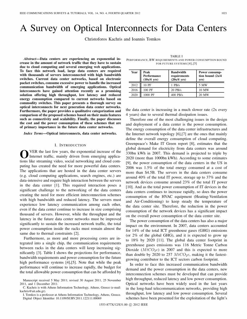
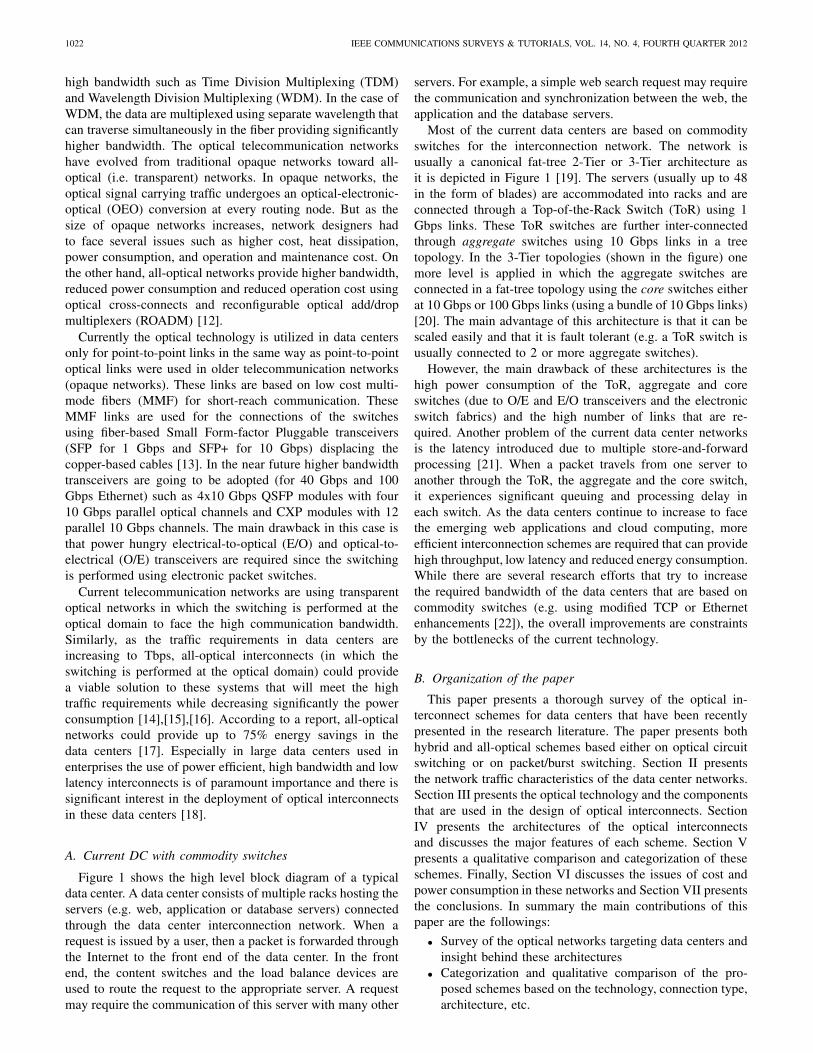
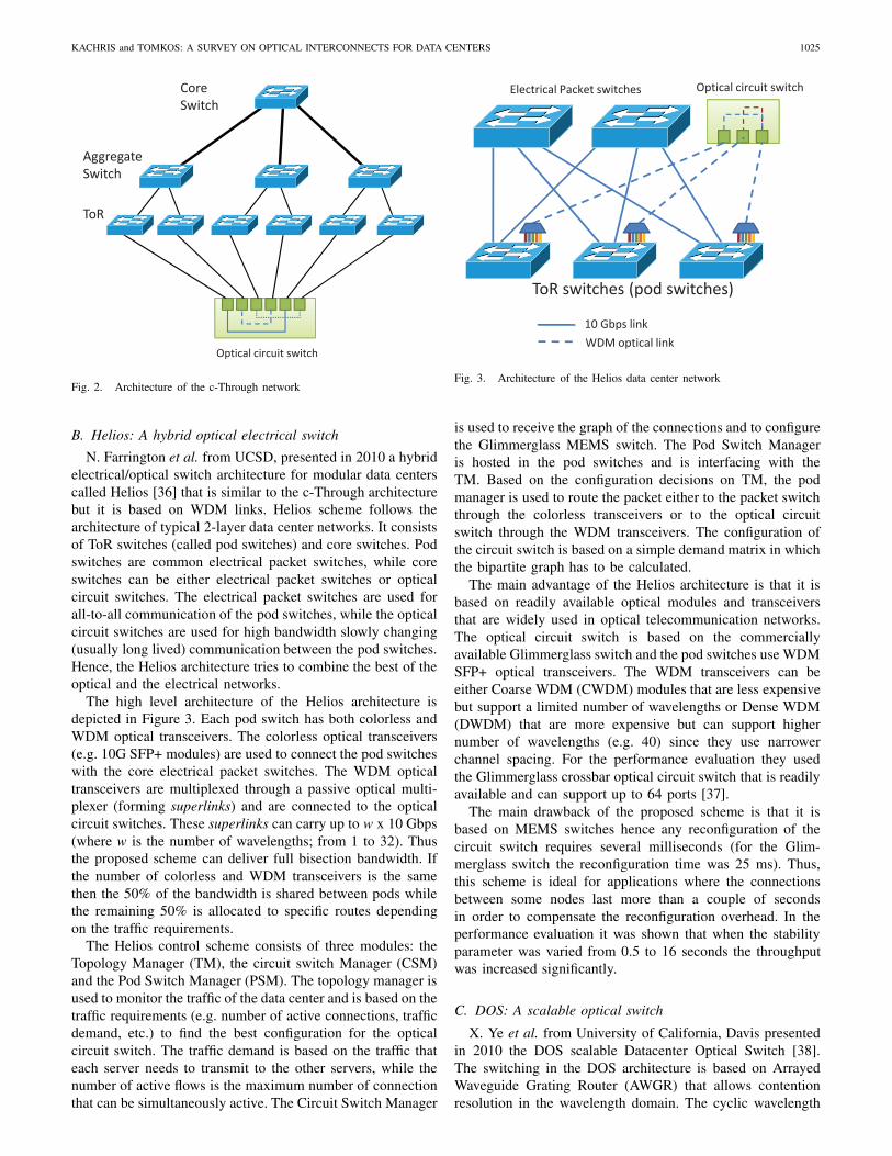
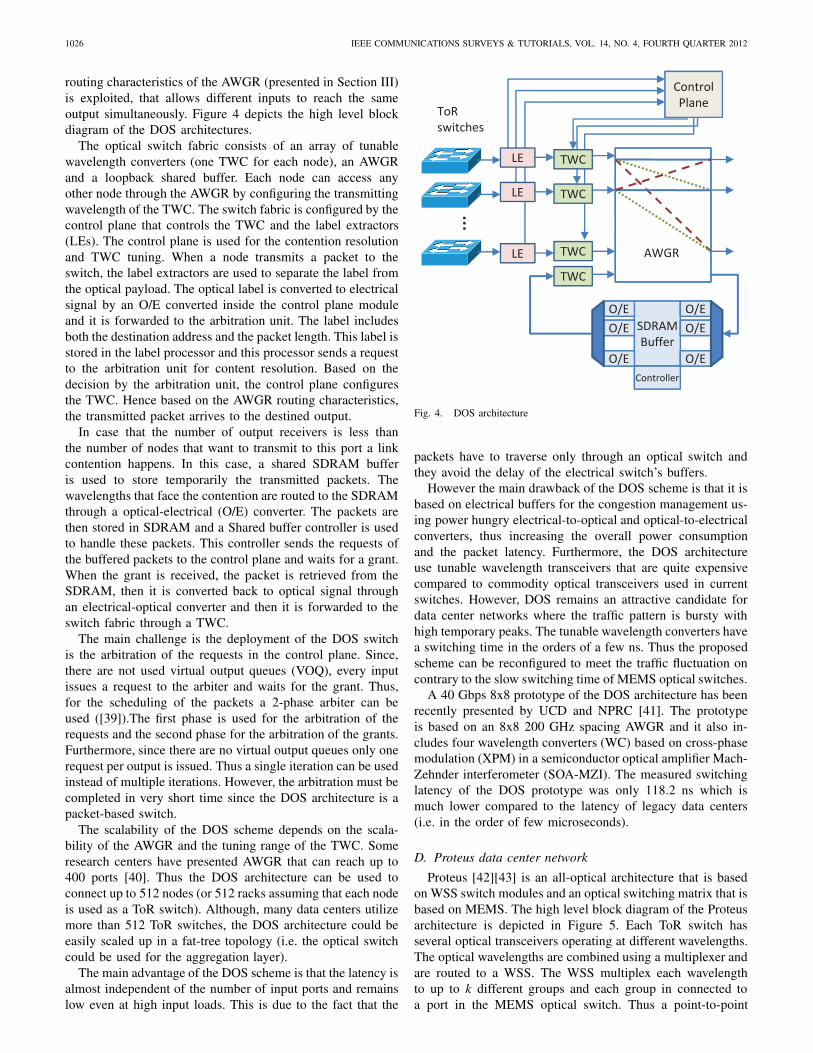
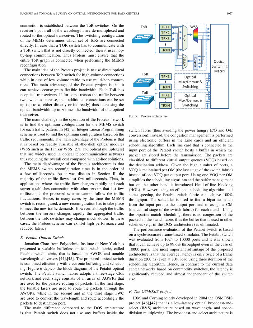


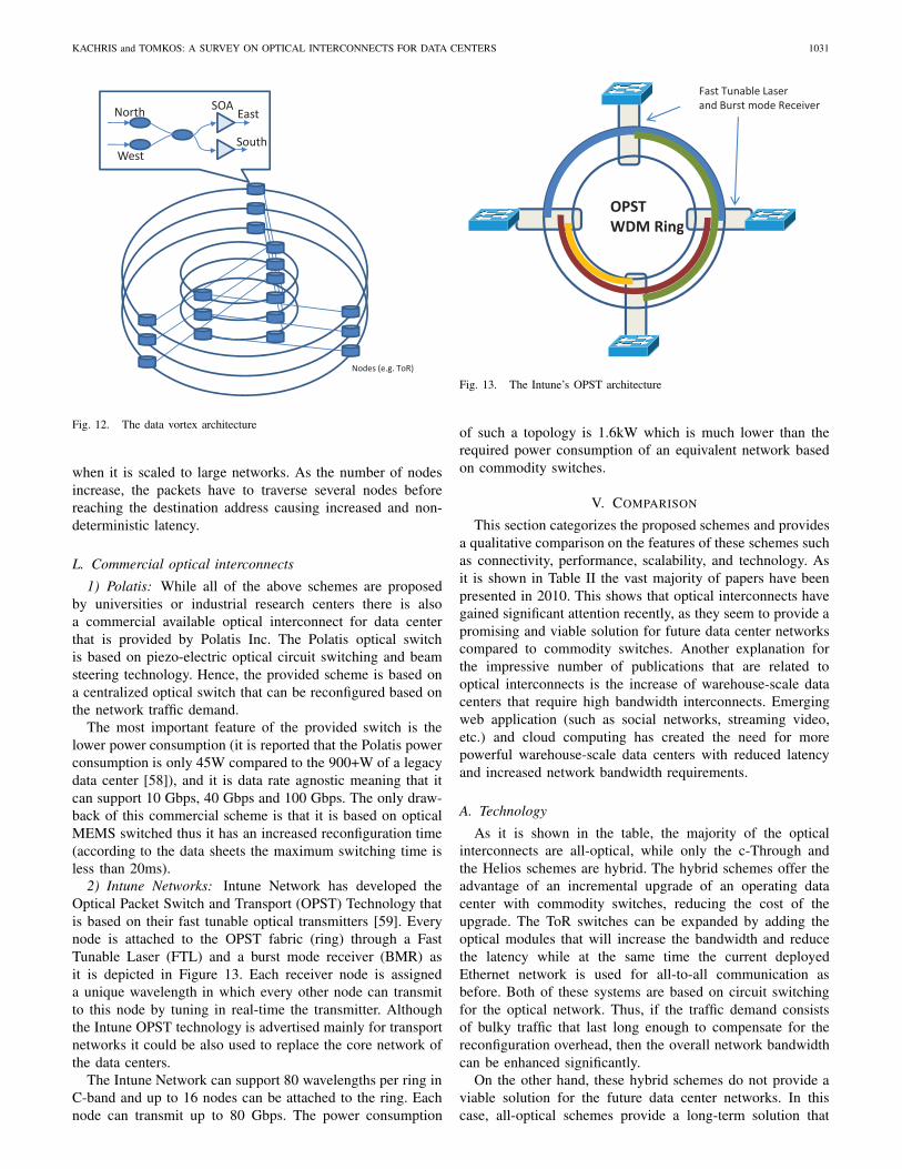
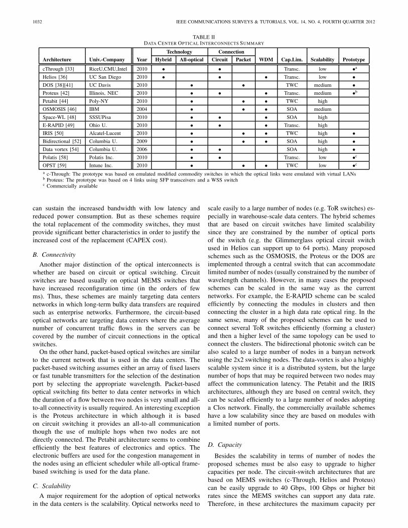


![IEEE COMMUNICATIONS SURVEYS & TUTORIALS, ACCEPTED …€¦ · · 2015-08-12ieee communications surveys & tutorials, accepted for publication 1 ... limitations and advantages [15].](https://static.documents.pub/doc/80x56/5ac0b2117f8b9ac6688c7b16/ieee-communications-surveys-tutorials-accepted-2015-08-12ieee-communications.jpg)


