Abstract— This letter proposes a novel high bit densitynonvolatile memory using a logic compatible flexible amorphousindium–gallium–zinc oxide (a-IGZO) thin-film transistor (TFT)structure fabricated at low temperature. Before electrical form-ing, the a-IGZO TFT exhibits excellent transistor performance,including an ON/OFF current ratio of 8.8 × 10⁶, a steepsubthreshold slope of 0.14 V/decade, a threshold voltage of0.55 V, and a maximum field-effect mobility of 2 cm2/Vs. Afterelectrical forming, a three-bit-per-cell resistive switching memoryis realized using localized multilevel resistance states at the drainand source bits. Combining dual functionalities to achieve low-cost integration and excellent device characteristics at bendingstates, the proposed device is promising for future system-on-plastic applications.
THE high-mobility amorphous indium–gallium–zinc oxide(a-IGZO) thin-film transistor (TFT) [1] has emerged
as a new generation active-matrix backplane technology inhigh-performance liquid crystal displays and organic light-emitting diode displays. It also enables the recently devel-oped flexible display technology because of its low processtemperature [2]. In addition, numerous logic circuits includ-ing logic gates, ring oscillators, shift registers, and staticrandom access memory [3]–[5] have also been successfullydemonstrated. Therefore, the high-mobility a-IGZO TFT tech-nology offers promising potential for monolithic system-on-plastic (SoP) integration in low-cost flexible electronics.Nonvolatile memory (NVM) is another essential buildingblock for a successful SoP integration. Several NVMs havebeen proposed with various degrees of compatibility withthe a-IGZO TFT technology. For example, a-IGZO memo-ries were fabricated using additional floating-gate or charge-trapping layers [6], [7]. The a-IGZO resistive-switching ran-dom access memory (RRAM) can be implemented in backend
Manuscript received July 16, 2013; accepted August 7, 2013. Date ofpublication September 11, 2013; date of current version September 23, 2013.This work was supported in part by the National Science Council of Taiwanunder Grant NSC 100-2628-E-009-025-MY2 and Grant 101-2221-E-009-089-MY3, and by the NCTU-UCB I-RiCE program under Grant NSC-102-2911-I-009-302. The review of this letter was arranged by Editor W. S. Wong.
The authors are with the Department of Electronics Engineering and theInstitute of Electronics, National Chiao Tung University, Hsinchu 30050,Taiwan (e-mail: [email protected]).
Color versions of one or more of the figures in this letter are availableonline at http://ieeexplore.ieee.org.
Digital Object Identifier 10.1109/LED.2013.2278098
Fig. 1. Cross-sectional diagrams of the staggered a-IGZO TFT using a four-mask process flow.
metallization processes [8], [9]. None of the mentioned devicescan be, however, integrated into the standard process flow ofa-IGZO TFTs without adding process steps and masks, whichpose significant challenges for device yields and the cost ofSoP integration.
Localized and independent resistive switching (RS) at drainand source bits in poly-Si TFTs [10] and a-IGZO TFTs[11] have been demonstrated using appropriate high-k gatedielectrics and metal gates. Its multibit-per-cell feature enablesextremely high bit-density and low-cost embedded NVM usinga completely logic compatible process flow. In addition tothe localized RS, multiple resistance states in RRAM [12]might be used to further increase bit density. The sameanalogy combining two distinct regions of charge storage andmultiple charge levels in a single cell has been used in high-density Flash memory [13]. In this letter, a three-bit-per-cellNVM technology was realized using localized multiple resis-tance states in a-IGZO TFTs. Excellent transistor and NVMcharacteristics can be achieved using an identical staggereda-IGZO TFT structure. The proposed device fabricated atlow temperature on a flexible substrate exhibited negligibledegradation at bending states, thereby promising for low-costSoP integration in the future.
II. EXPERIMENTAL PROCEDURE
Fig. 1 shows a staggered a-IGZO TFT fabricated using afour-mask process flow on a flexible polyimide (PI) substrate.Before the device fabrication, a 75-µm-thick Kapton PI filmwas cut to a size of 7 cm × 7 cm and cleaned using acetoneto remove particles, followed by baking at 100 °C for 30 min.
1266 IEEE ELECTRON DEVICE LETTERS, VOL. 34, NO. 10, OCTOBER 2013
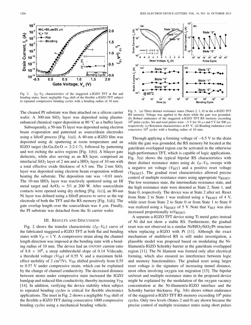
Fig. 2. ID–VG characteristics of the staggered a-IGZO TFT at flat andbending states. Inset: negligible VTH shift of the flexible a-IGZO TFT subjectto repeated compressive bending cycles with a bending radius of 10 mm.
The cleaned PI substrate was then attached on a silicon carrierwafer. A 300-nm SiO2 layer was deposited using plasma-enhanced chemical vapor deposition at 80 °C as a buffer layer.
Subsequently, a 50-nm Ti layer was deposited using electronbeam evaporation and patterned as source/drain electrodesusing a liftoff process [Fig. 1(a)]. A 40-nm a-IGZO film wasdeposited using dc sputtering at room temperature and anIGZO target (In:Ga:Zn:O = 2:2:1:7), followed by patterningand wet etching the active regions [Fig. 1(b)]. A bilayer gatedielectric, while also serving as an RS layer, comprised aninterfacial SiO2 layer of 2 nm and a HfO2 layer of 10 nm witha total effective oxide thickness of 4.5 nm. The 2-nm SiO2layer was deposited using electron beam evaporation withoutheating the substrate. The deposition rate was ∼0.01 nm/s.The 10-nm HfO2 layer was reactively sputtered using an Hfmetal target and Ar/O2 = 5/1 at 200 W. After source/draincontacts were opened using dry etching [Fig. 1(c)], an 80-nmNi layer was defined using a liftoff process to serve as the topelectrode of both the TFT and the RS memory [Fig. 1(d)]. Thegate overlap length over the source/drain was 4 µm. Finally,the PI substrate was detached from the Si carrier wafer.
III. RESULTS AND DISCUSSION
Fig. 2 shows the transfer characteristic (ID–VG) curve ofthe fabricated staggered a-IGZO TFT at both flat and bendingstates with VD = 1 V. A compressive strain along the channellength direction was imposed at the bending state with a bend-ing radius of 10 mm. The device had an ON/OFF current ratioof 8.8 × 10⁶, a steep subthreshold slope of 0.14 V/decade,a threshold voltage (VTH) of 0.55 V, and a maximum field-effect mobility of 2 cm2/Vs. VTH shifted positively from 0.55to 0.57 V under compressive strain, which can be explainedby the change of channel conductivity. The decreased distancebetween atoms under compressive stain increased the IGZObandgap and reduced film conductivity, thereby increasing VTH[14]. In addition, verifying the device stability when subjectto repeated bending cycles is critical for flexible electronicsapplications. The inset in Fig. 2 shows a negligible VTH shift ofthe flexible a-IGZO TFT during consecutive 1000 compressivebending cycles using a mechanical bending vehicle.
Fig. 3. (a) Three distinct resistance states (States 2, 1, 0) in the a-IGZO TFTRS memory. Voltage was applied to the drain while the gate was grounded.(b) Robust endurance of the staggered a-IGZO TFT RS memory exceeding106 pulse cycles. Set and reset pulses were −5 V for 10 µs and 5 V for 500 µs,respectively. (c) Retention characteristics at 85 °C. (d) Bending endurance overconcessive 104 cycles with a bending radius of 10 mm.
Through applying a forming voltage of −6.5 V to the drainwhile the gate was grounded, the RS memory bit located at thegate/drain overlapped region can be activated in the otherwisehigh-performance TFT, which is capable of logic applications.Fig. 3(a) shows the typical bipolar RS characteristics withthree distinct resistance states using dc ID–VD sweeps witha negative set voltage (VSET) and a positive reset voltage(VRESET). The gradual reset characteristics allowed precisecontrol of multiple resistance states using appropriate VRESET.The low resistance state, the intermediate resistance state, andthe high resistance state were denoted as State 2, State 1, andState 0, respectively. The device was at State 2 after set. Resetfrom State 2 to State 1 was realized using a VRESET of 4 V,while reset from State 2 to State 0 or from State 1 to State 0was realized using a VRESET of 5 V. Note that VSET was alsoincreased proportionally toVRESET.
A separate a-IGZO TFT device using Ti metal gates insteadof Ni did not show a stable RS. Furthermore, the gradualreset was not observed in a similar Ni/HfO2/SiO2/Pt structurewhen replacing a-IGZO with Pt [11]. Although the exactmechanism of multilevel RS is still under investigation, aplausible model was proposed based on modulating the Ni-filament/a-IGZO Schottky barrier at the gate/drain overlappedregion [11]. The Ni filament was formed only after electricalforming, which also ensured no interference between logicand memory functionalities. The gradual reset using largerreset voltage is the signature of increasing tunnel distance,most often involving oxygen ion migration [15]. The bipolarset/reset and multiple resistance states in the proposed devicemight be explained by the modulation of the oxygen vacancyconcentration at the Ni-filament/a-IGZO interface and theSchottky barrier thickness. Fig. 3(b) shows robust enduranceof the staggered a-IGZO TFT RS memory exceeding 106 pulsecycles. Only two levels (States 2 and 0) are shown because theprecise control of multiple resistance states using short pulses
WU et al.: FLEXIBLE THREE-BIT-PER-CELL RS MEMORY 1267
Fig. 4. (a) Schematic diagram of a-IGZO TFT RS memory array. One-transistor unit cell contains two 3-state bits. Two bit lines BLSD and BLSS areused to read out ID at the drain bit and IS at the source bit simultaneously.(b) Simultaneous ID and IS readout of an operating sequence through allnine available states, 00 (D:HRS; S:HRS) →20 (D:LRS; S:HRS) → 22(D:LRS; S:LRS) → 21 (D:LRS; S:IRS) →11 (D:IRS; S:IRS) →10 (D:IRS;S:HRS) → 12 (D:IRS; S:LRS) → 02 (D:HRS; S:LRS) → 01 (D:HRS;S:IRS) → 00 (D:HRS; S:HRS) for one cycle (left) and for 30 cycles (right).
was more difficult to achieve in the present standalone devicewithout current-limiting transistors. Fig. 3(c) shows the stableretention characteristics of three resistance states at 85 °C.Finally, Fig. 3(d) shows superior bending endurance exceeding104 consecutive cycles.
Similar RS characteristics were also achieved at the sourcebit. RS can be precisely controlled at the drain/source bitswithout interference by suppressing the coupling through thea-IGZO channel. The independent RS was guaranteed whenthe channel current was less than that required for set andreset by choosing appropriate device dimensions. Combiningtwo three-state bits at the drain and source, total nine states(32) could be defined using simultaneous readouts of ID andIS in an one-transistor unit cell, as shown in Fig. 4(a) [10].For instance, the memory state 00 and 20 denoted when thedrain/source bits were at State 0/State 0 and State 2/State 0,respectively. Using two bit lines and appropriate peripheralprogram/read circuits, the one-transistor unit cell is capableof storing three-bit data which requires 23 states. Fig. 4(b)shows simultaneous ID and IS readouts using a switchingsequence through all nine available states in a device with achannel width and length of 20 and 10 µm, respectively. Thestate of the drain bit remained unaltered when the source bitwas programmed, and vice versa, showing negligible interfer-ence between two physical bits. The results demonstrated thefirst three-bit-per-cell RRAM using localized multilevel RS.
Enlarging the maximum resistance ratio in the future mightadd more distinct levels to each localized bit and furtherincrease bit density.
IV. CONCLUSION
This letter demonstrated a novel flexible NVM technologyusing logic compatible a-IGZO TFTs fabricated at low tem-perature. Independent multilevel RS at the drain and sourcebits enabled reliable three-bit-per-cell operations. In additionto the excellent flexible memory characteristics and highbit density, the a-IGZO TFTs without undergoing electricalforming showed promising transistor performance and bendingstability. This letter suggests that both logic circuits andNVM can be seamlessly integrated on the flexible substrateusing an identical a-IGZO TFT technology, which creates newopportunities for future SoP applications.
REFERENCES
[1] K. Nomura, H. Ohta, A. Takagi, et al., “Room-temperature fabricationof transparent flexible thin-film transistors using amorphous oxide semi-conductors,” Nature, vol. 432, no. 7016, pp. 488–492, 2004.
[2] J. S. Park, T. W. Kim, D. Stryakhilev, et al., “Flexible full color organiclight-emitting diode display on polyimide plastic substrate driven byamorphous indium gallium zinc oxide thin-film transistors,” Appl. Phys.Lett., vol. 95, no. 1, pp. 013503-1–013503-3, 2009.
[3] H. Luo, P. Wellenius, L. Lunardi, et al., “Transparent IGZO-basedlogic gates,” IEEE Electron Device Lett., vol. 33, no. 5, pp. 673–675,May 2012.
[4] M. Mativenga, M. H. Choi, J. W. Choi, et al., “Transparent flexi-ble circuits based on amorphous-indium-gallium-zinc-oxide thin-filmtransistors,” IEEE Electron Device Lett., vol. 32, no. 2, pp. 170–172,Feb. 2011.
[5] N. Münzenrieder, C. Zysset, T. Kinkeldei, et al., “A flexible InGaZnObased 1-bit SRAM under mechanical strain,” in Proc. Semicond. Conf.Dresden, 2011, pp. 1–4.
[6] H. Yin, S. Kim, H. Lim, et al., “Program/erase characteristics ofamorphous gallium indium zinc oxide nonvolatile memory,” IEEE Trans.Electron Devices, vol. 55, no. 8, pp. 2071–2077, Aug. 2008.
[7] J. Jang, J. C. Park, D. Kong, et al., “Endurance characteristics ofamorphous-InGaZnO transparent flash memory with gold nanocrys-tal storage layer,” IEEE Trans. Electron Devices, vol. 58, no. 11,pp. 3940–3947, Nov. 2011.
[8] M. C. Chen, T. C. Chang, C. T. Tsai, et al., “Influence of elec-trode material on the resistive memory switching property of indiumgallium zinc oxide thin films,” Appl. Phys. Lett., vol. 96, no. 26,pp. 262110-1–262110-3, 2010.
[9] Q. Wang, H. Y. Xu, X. H. Li, et al., “Flexible resistive switching memorydevice based on amorphous InGaZnO film with excellent mechanicalendurance,” IEEE Electron Device Lett., vol. 32, no. 10, pp. 1442–1444,Oct. 2011.
[10] S. C. Wu, C. Lo, and T. H. Hou, “Novel two-bit-per-cell resistive-switching memory for low-cost embedded applications,” IEEE ElectronDevice Lett., vol. 32, no. 12, pp. 1662–1664, Dec. 2011.
[11] S. C. Wu, H. T. Feng, M. J. Yu, et al., “Multi-bit-per-cell a-IGZO TFTresistive-switching memory for system-on-plastic applications,” in IEDMTech. Dig., 2012, pp. 100–103.
[12] C. Yoshida, K. Tsunoda, H. Noshiro, et al., “High speed resis-tive switching in Pt/TiO2/TiN film for nonvolatile memory applica-tion,” Appl. Phys. Lett., vol. 91, no. 22, pp. 223510-1–223510-3,2007.
[13] B. Eitan, G. Cohen, A. Shappir, et al., “4-bit per cell NROM reliability,”in IEDM Tech. Dig., 2005, pp. 539–542.
[14] N. Münzenrieder, K. H. Cherenack, and G. Tröster, “The effects ofmechanical bending and illumination on the performance of flex-ible IGZO TFTs,” IEEE Trans. Electron Devices, vol. 58, no. 7,pp. 2041–2048, Jul. 2011.
[15] S. Yu, X. Guan, and H.-S. P. Wong, “On the stochastic nature ofresistive switching in metal oxide RRAM: Physical modeling, MonteCarlo simulation, and experimental characterization,” in IEDM Tech.Dig., 2011, pp. 413–416.